
Ultraviolet Photodetectors: From Photocathodes to Low-Dimensional Solids


Abstract
:1. Introduction
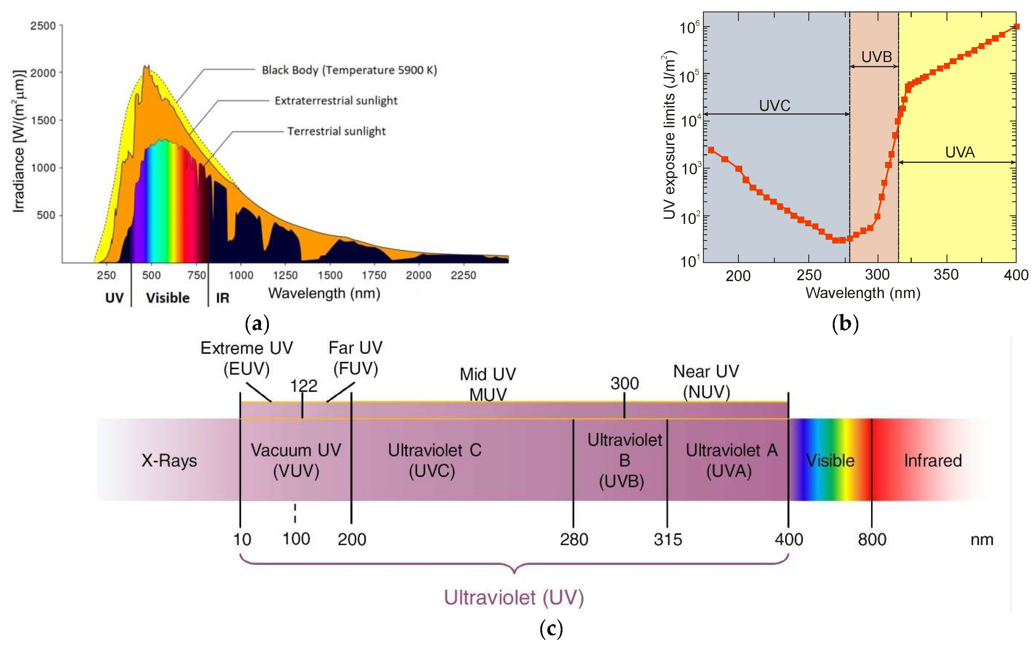
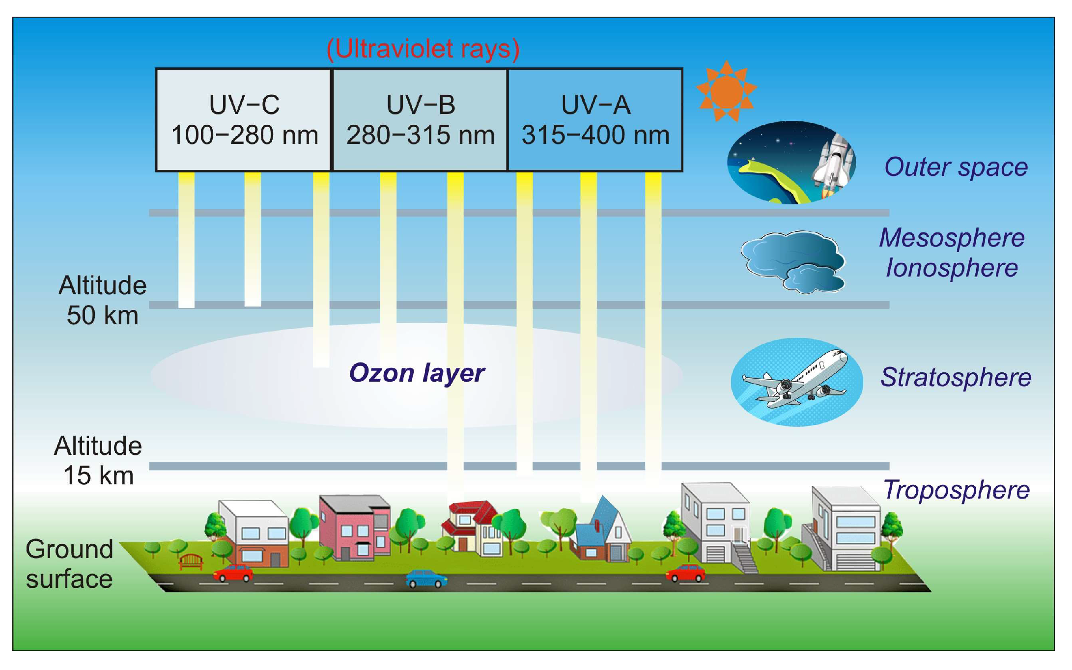
- UV-A—wavelengths: 315–400 nm;
- UV-B—wavelengths: 280–315 nm;
- UV-C—wavelengths: 100–280 nm.
- Not light-sensitive (solar blind);
- High quantum efficiency;
- High dynamic range of operation;
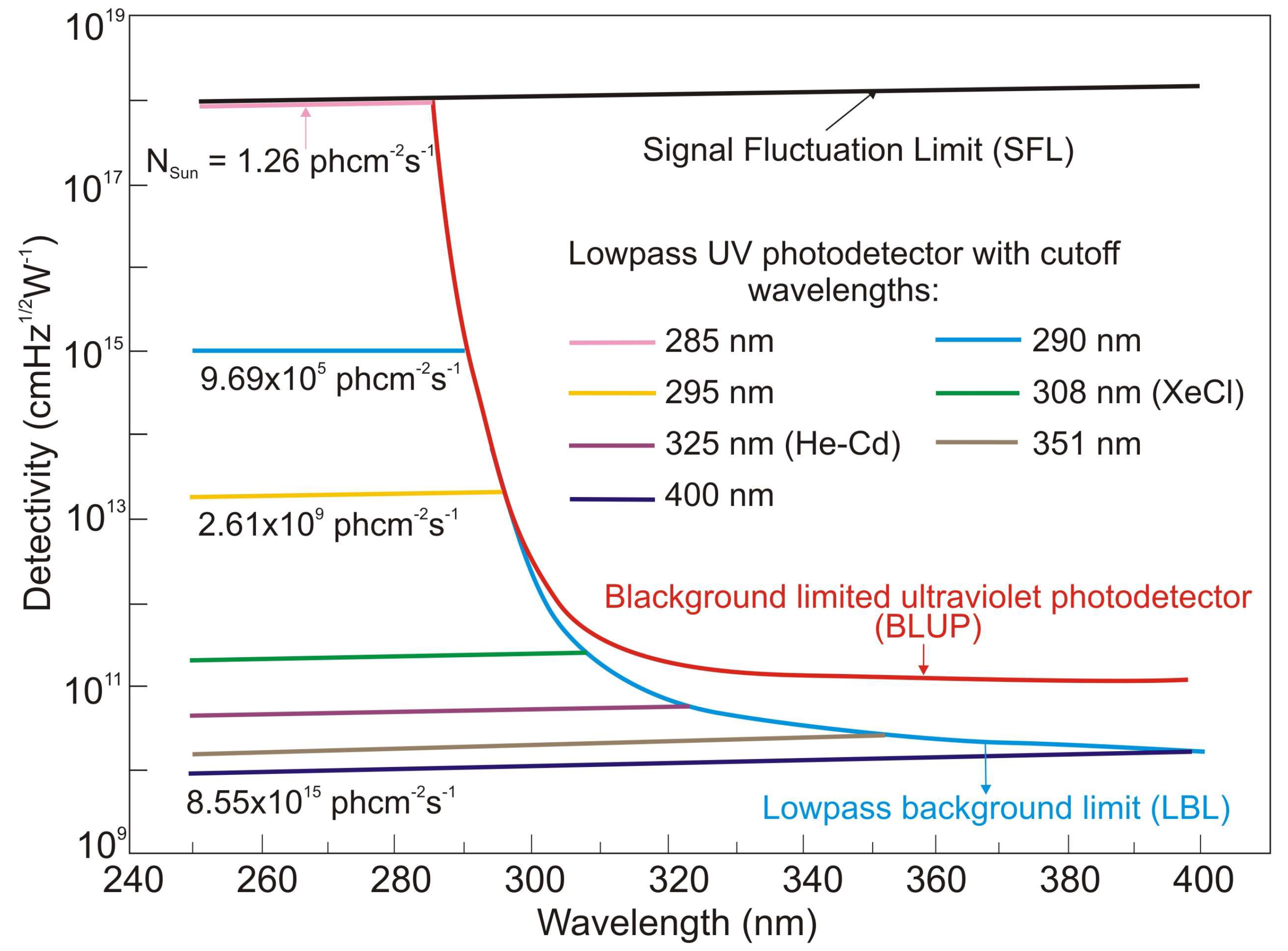
- Low background and floor noise often dominate observations of the weak UV.
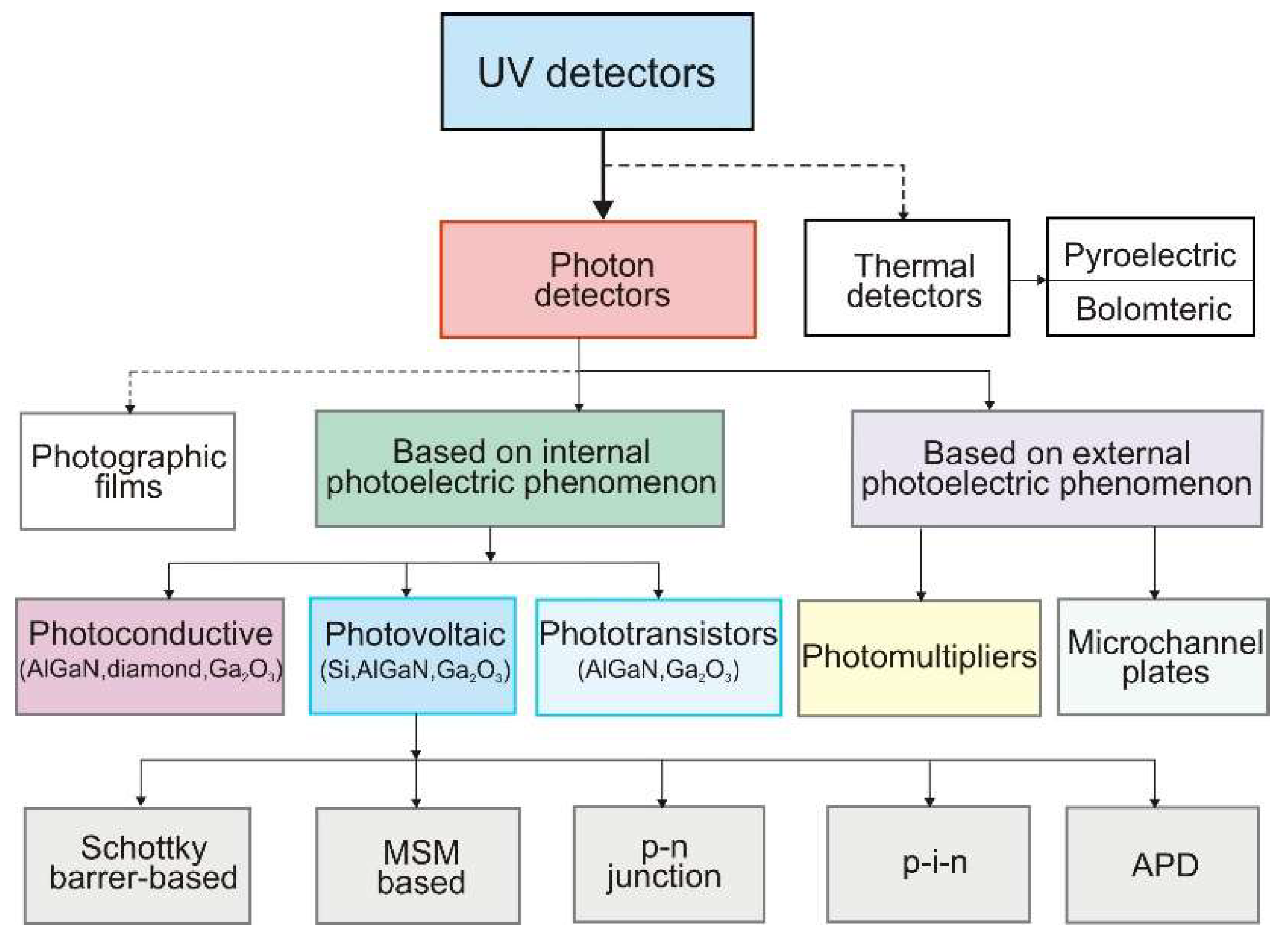
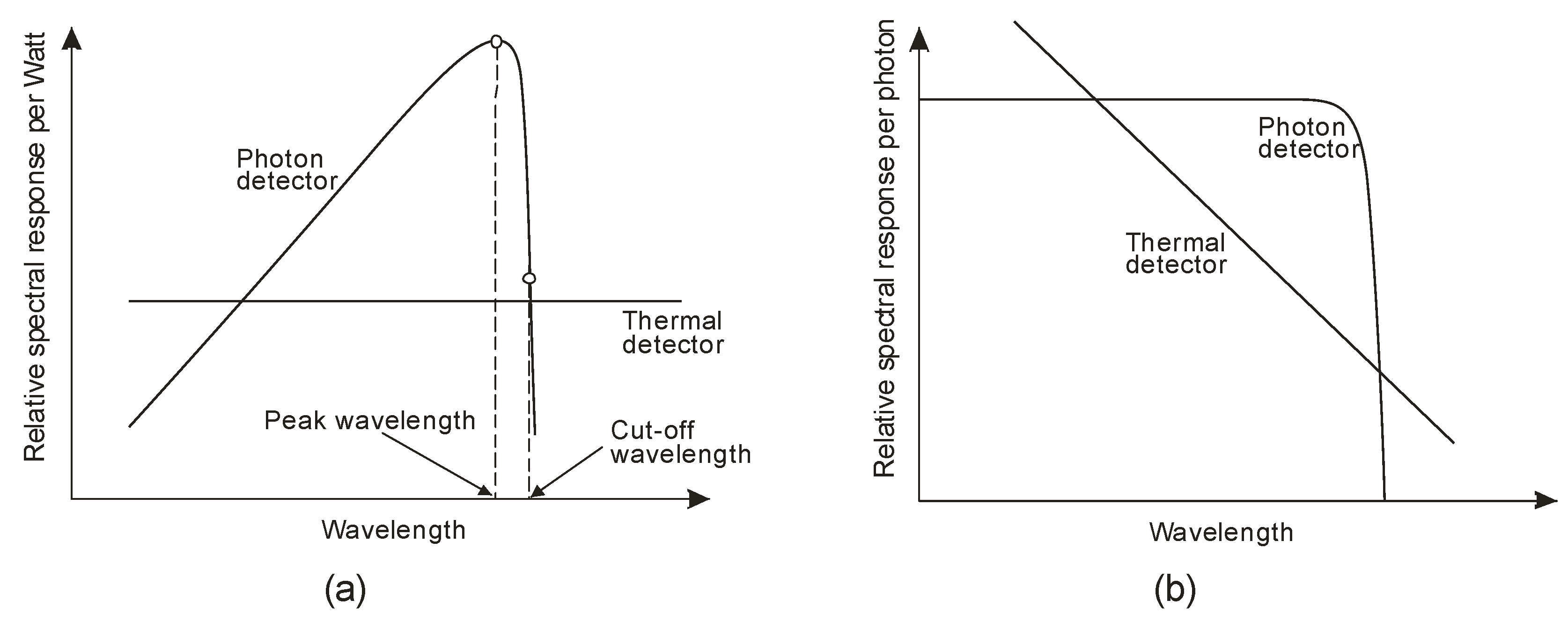
2. General Theory of Photodetectors
- Inadequacy of detectivity specifications based on responsivity and noise (shot noise and generation-recombination noise);
- Lack of properly refined protocols for accurately determining figure-of-merit for photodetectors (especially for the new-generation of two-dimensional (2D) and quasi-2D material ones).
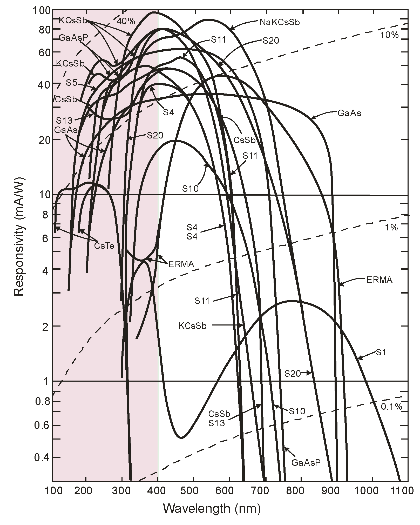
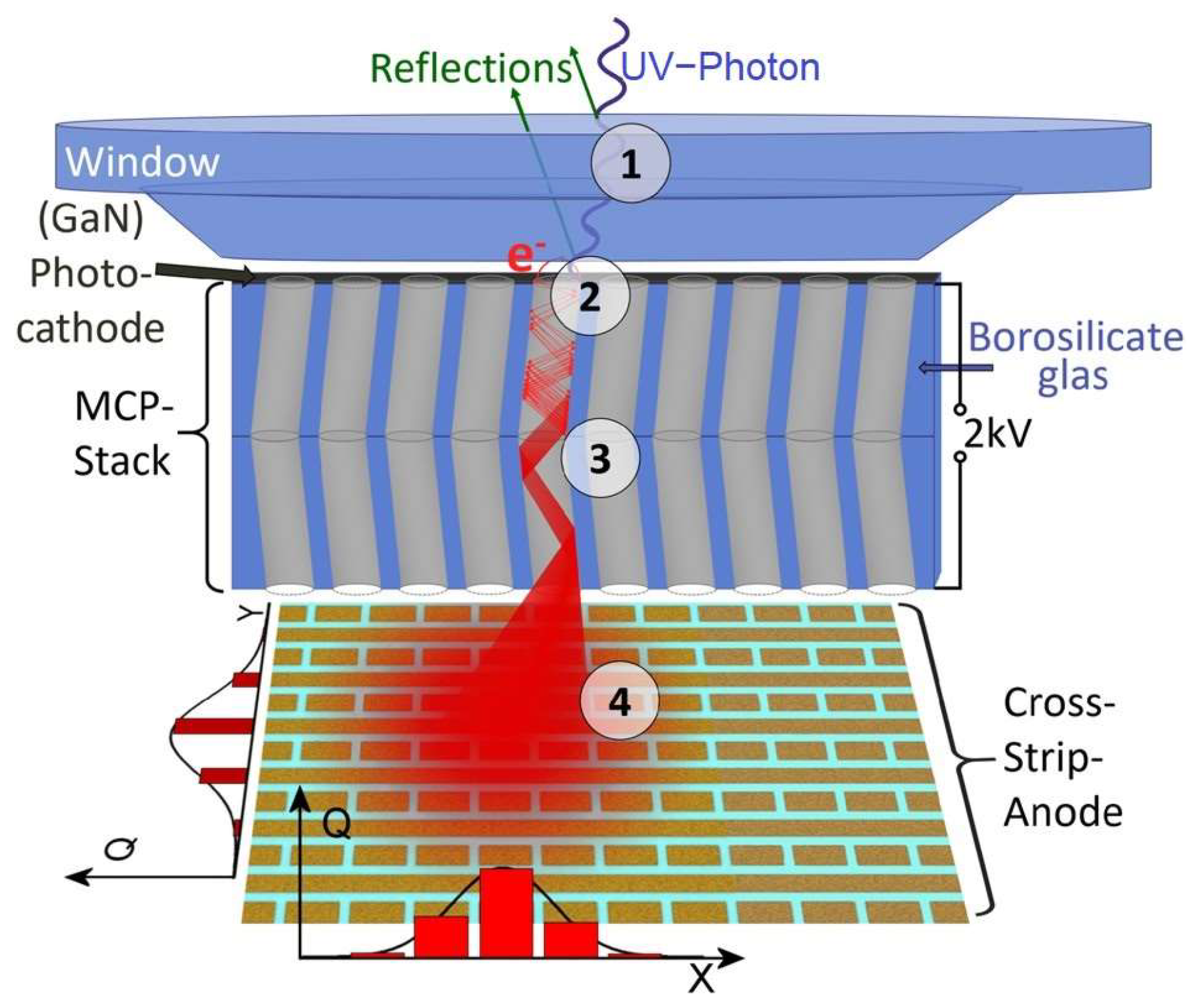
3. Photoemissive Detectors
- Incoming UV radiation passes through a window (fused silica/MgF2/LiF);
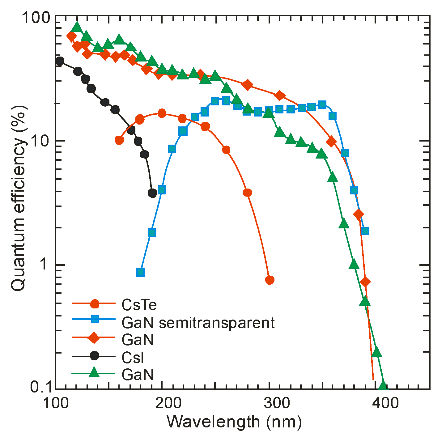
- The photocathode converts the radiation into photoelectrons; the degree of conversion depends on the photocathode material and the wavelength of the incident radiation (estimated to reach as high as 70% at 230 nm for GaN);
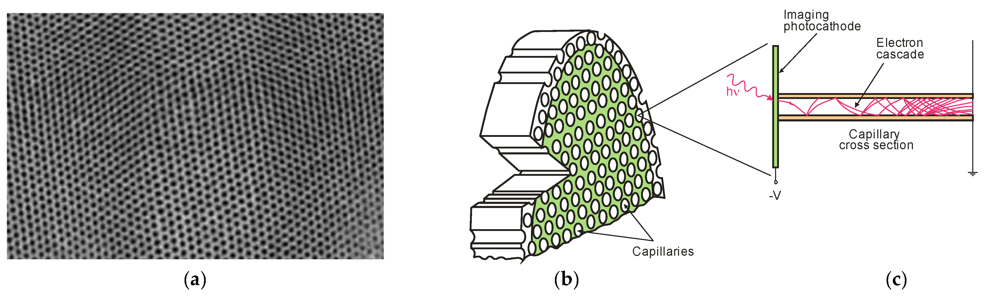
- A high voltage of the order of 2 kV accelerates the incident photoelectrons in microchannel plates (MCPs), resulting in a charge of, e.g., 105 to 106 electrons on the bottom side of the MCP stack;
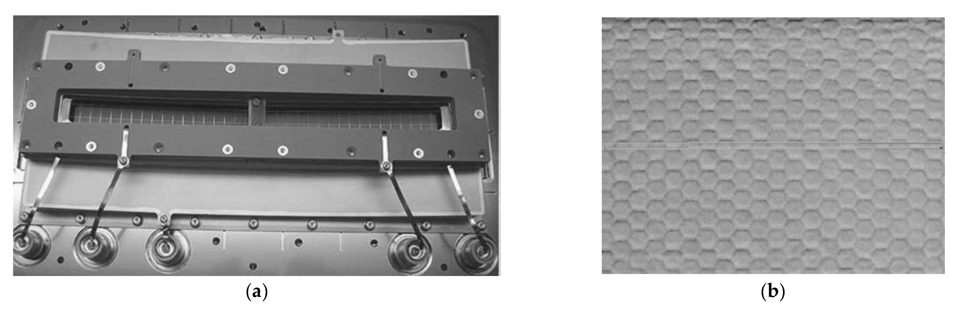
- The electron cloud is accelerated towards the anode with a cross stripe (64 strips in the X direction and 64 strips in the Y direction).
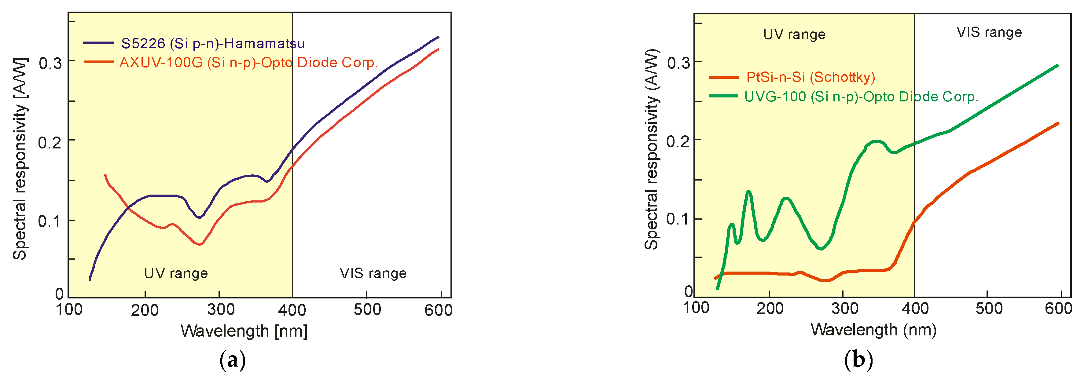
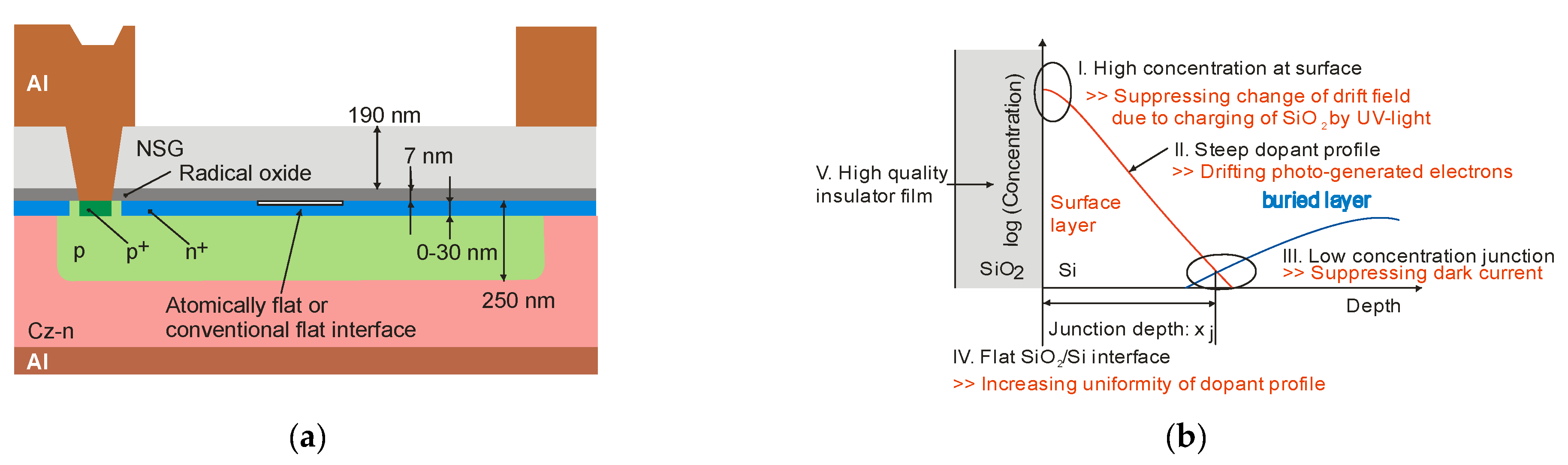
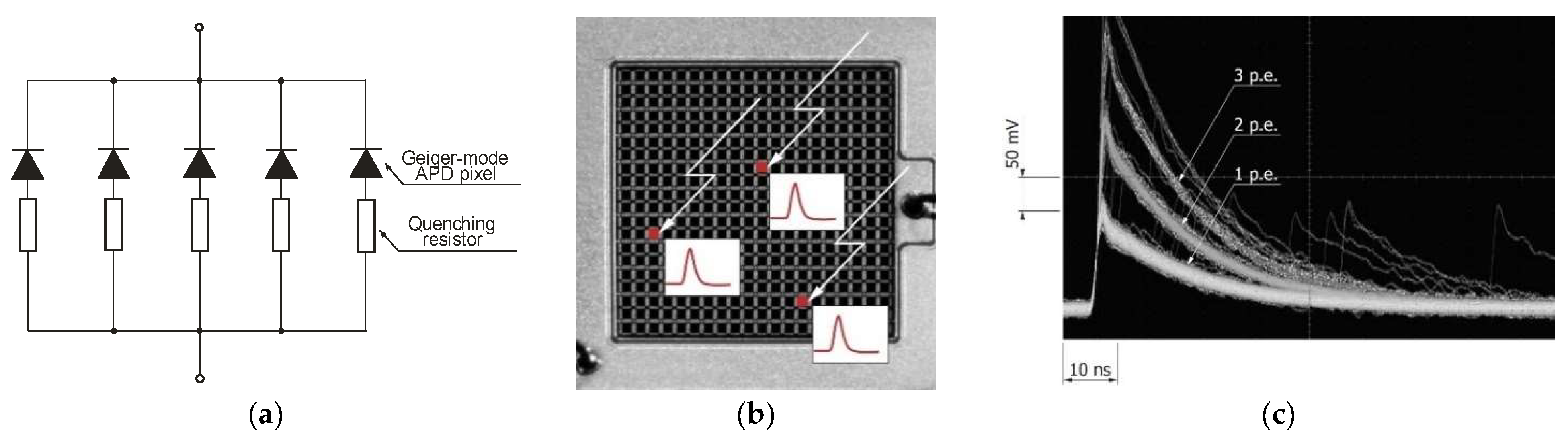
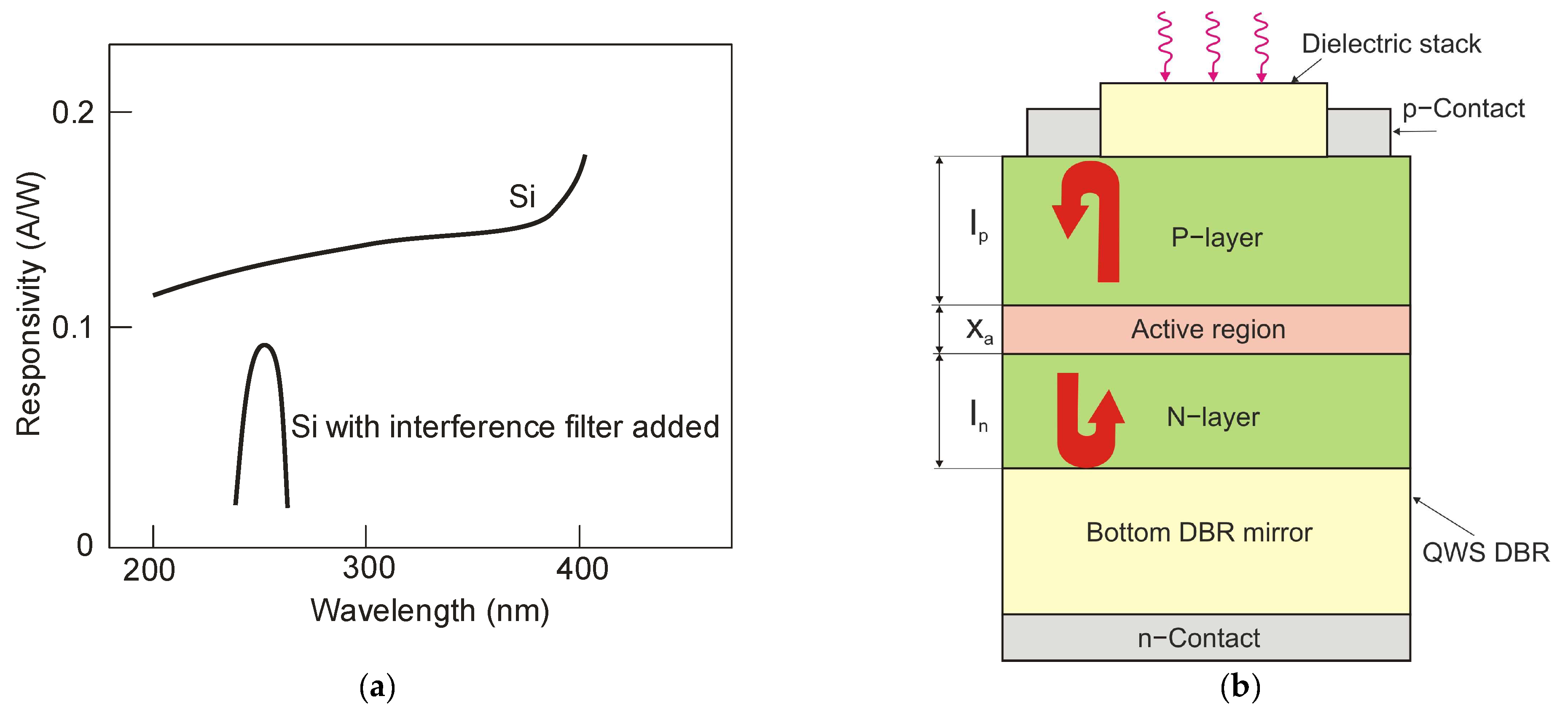
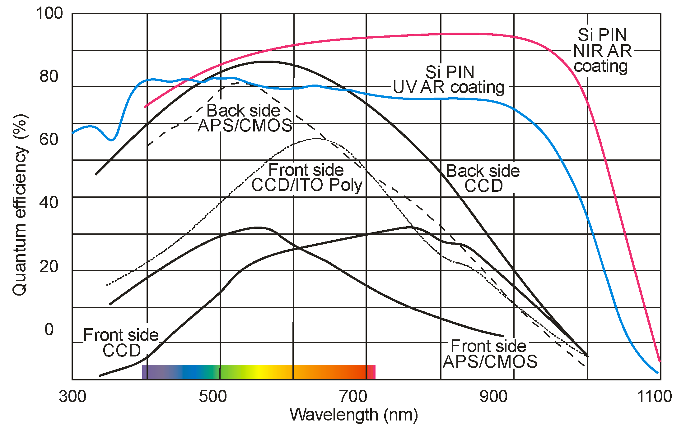
4. Silicon-Based Photodetectors

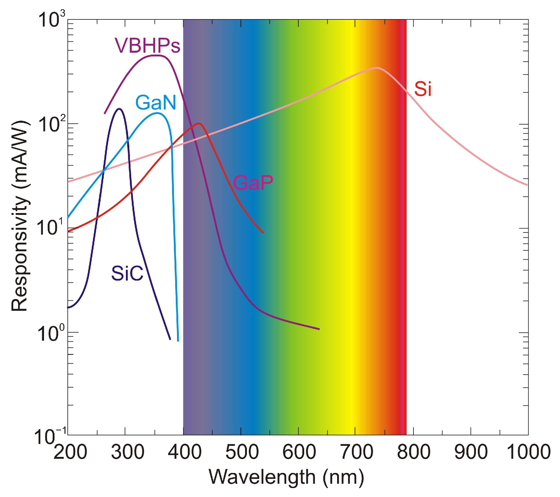
5. Wide Bandgap UV Photodetectors
5.1. AlGaN Photodetectors
5.1.1. Photoconductors
5.1.2. Schottky Barrier Photodiodes
5.1.3. p–n Photodiodes

5.1.4. Phototransistors
5.1.5. Focal Plane Arrays
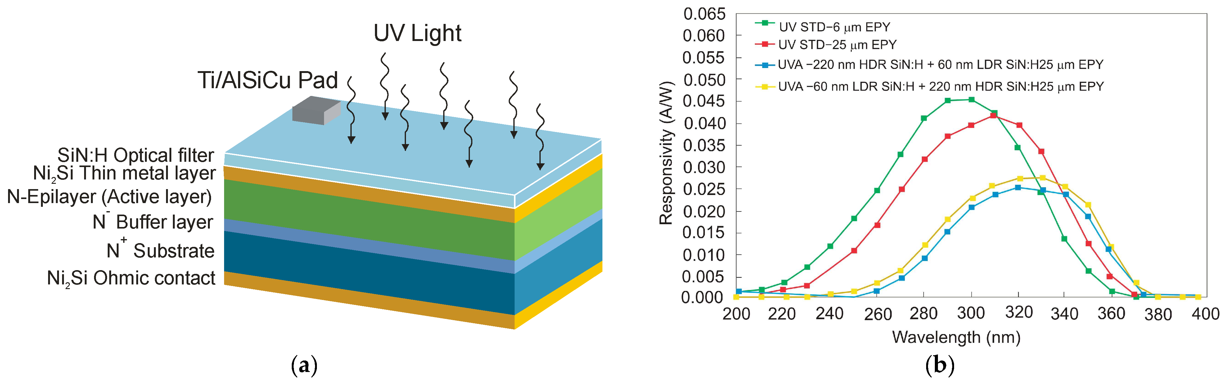
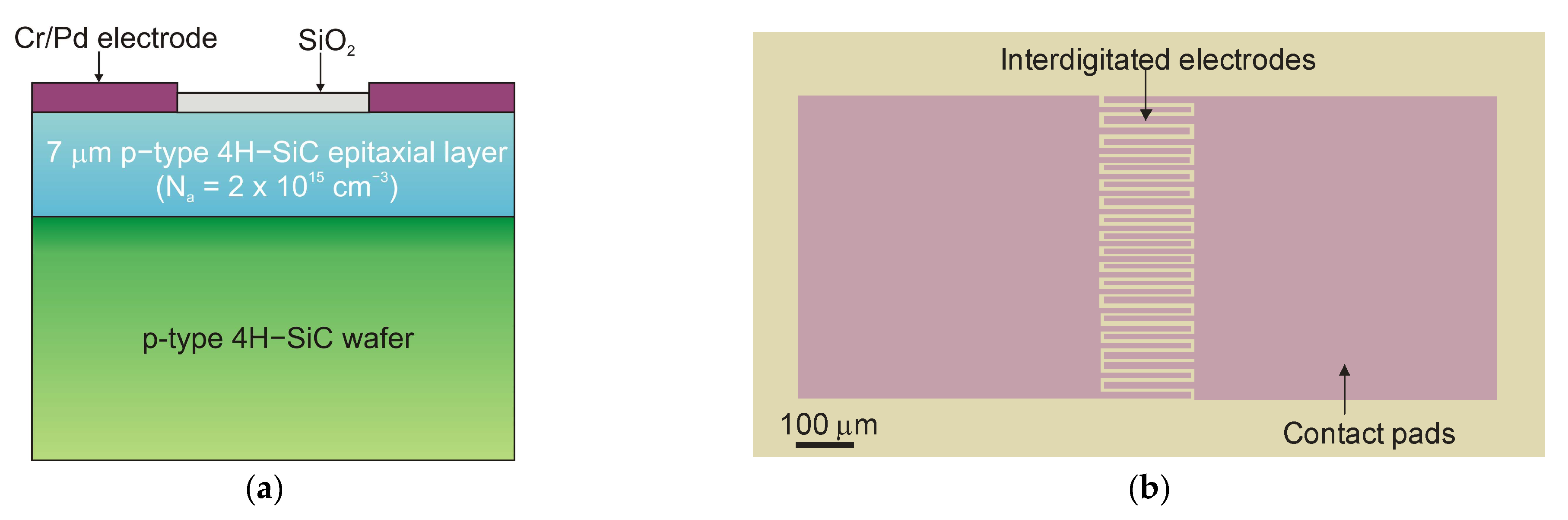
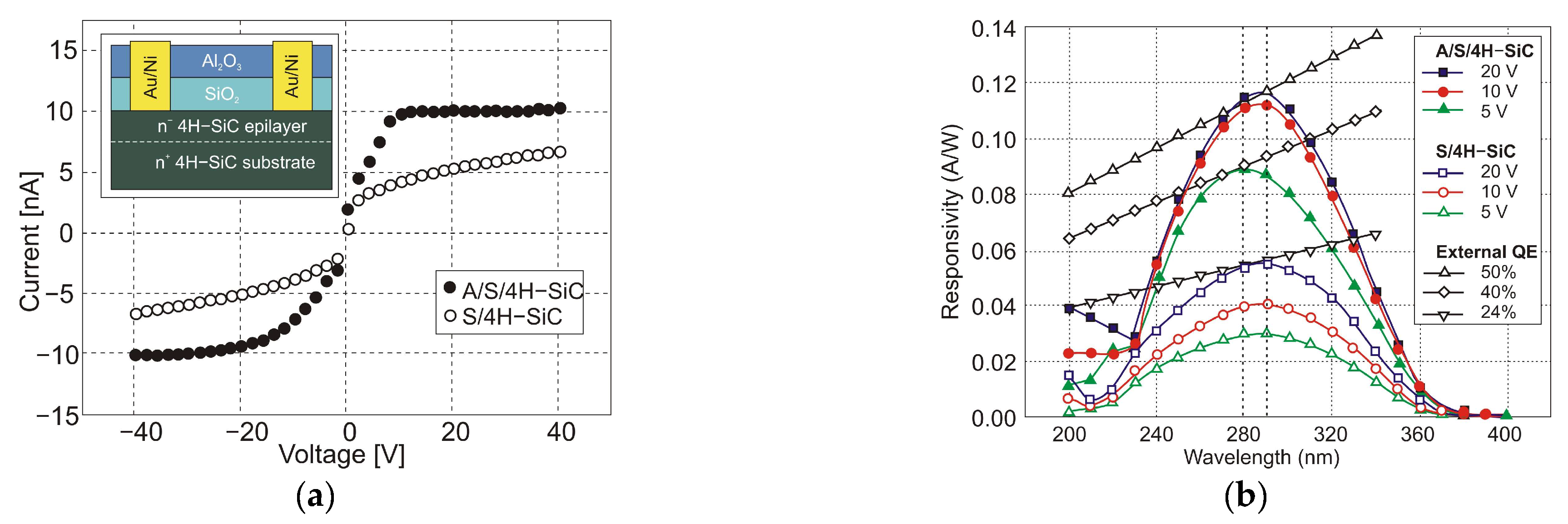
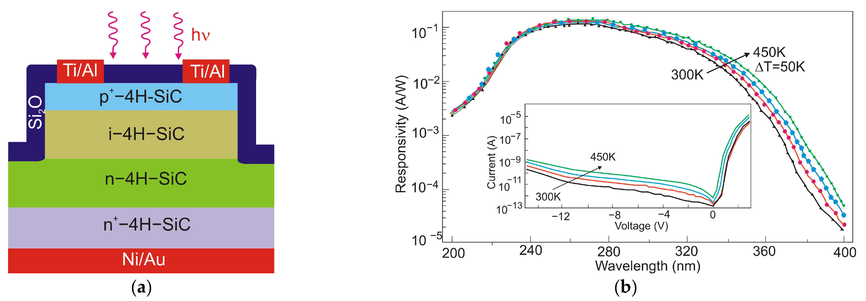
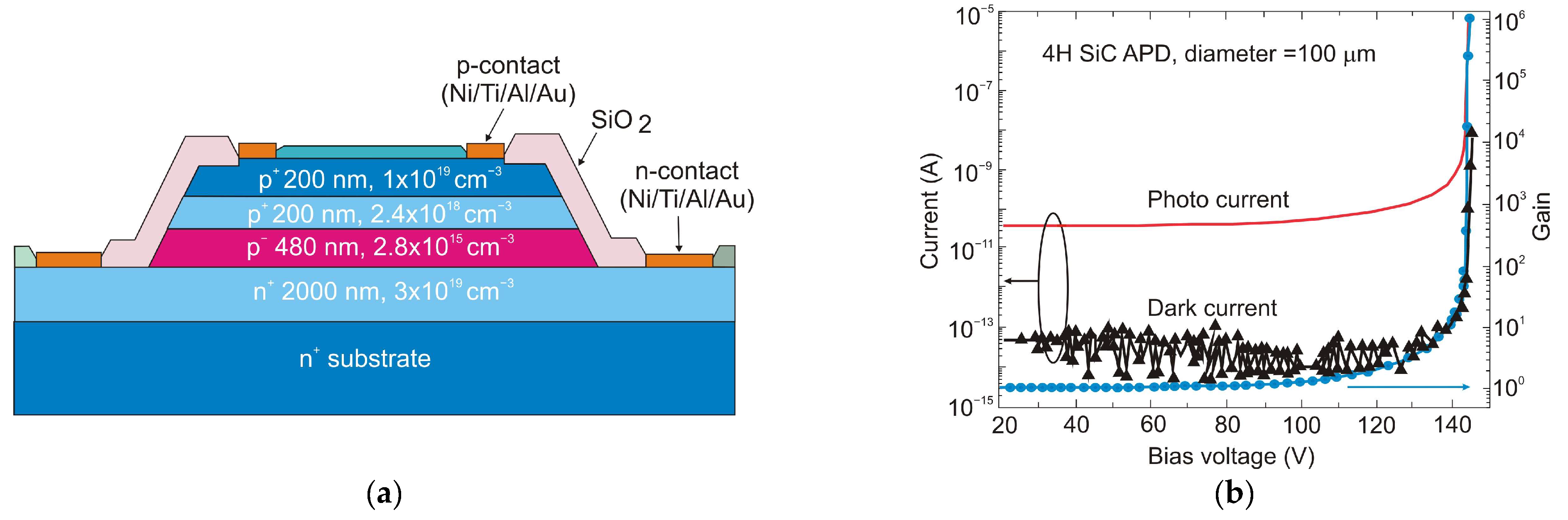
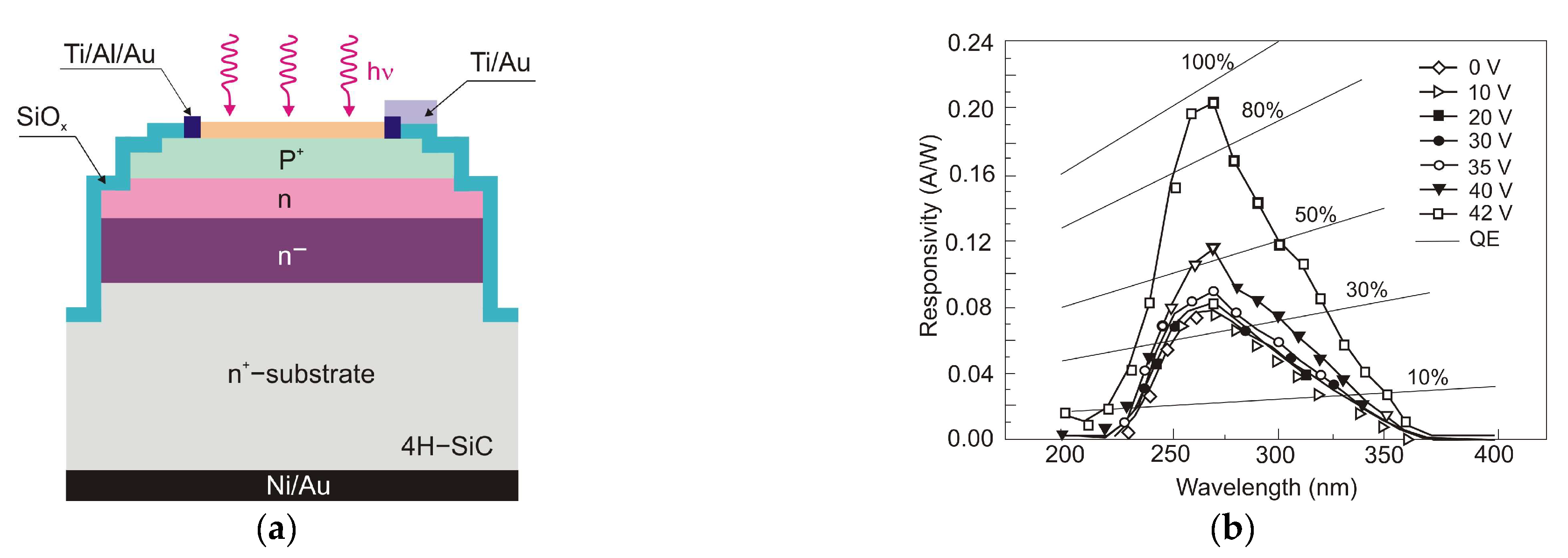
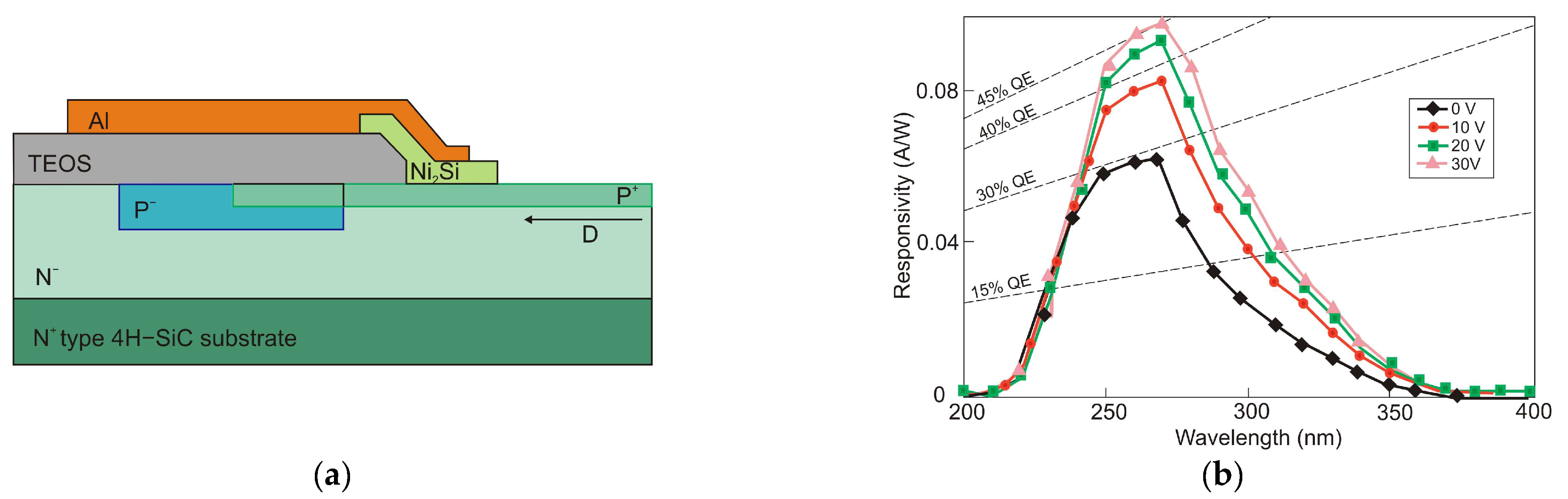
5.2. SiC-Based Photodetectors
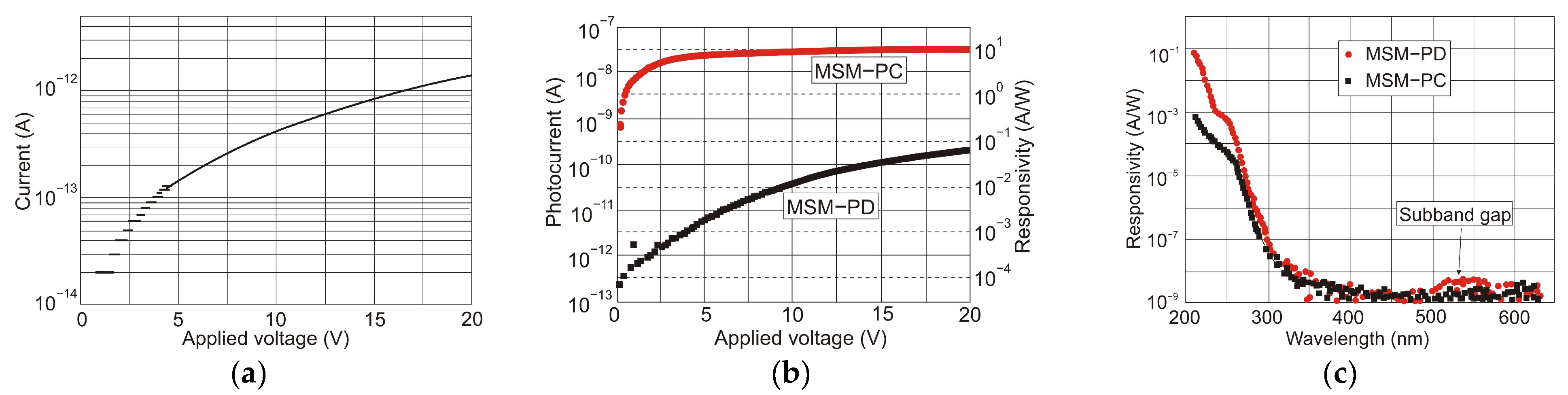
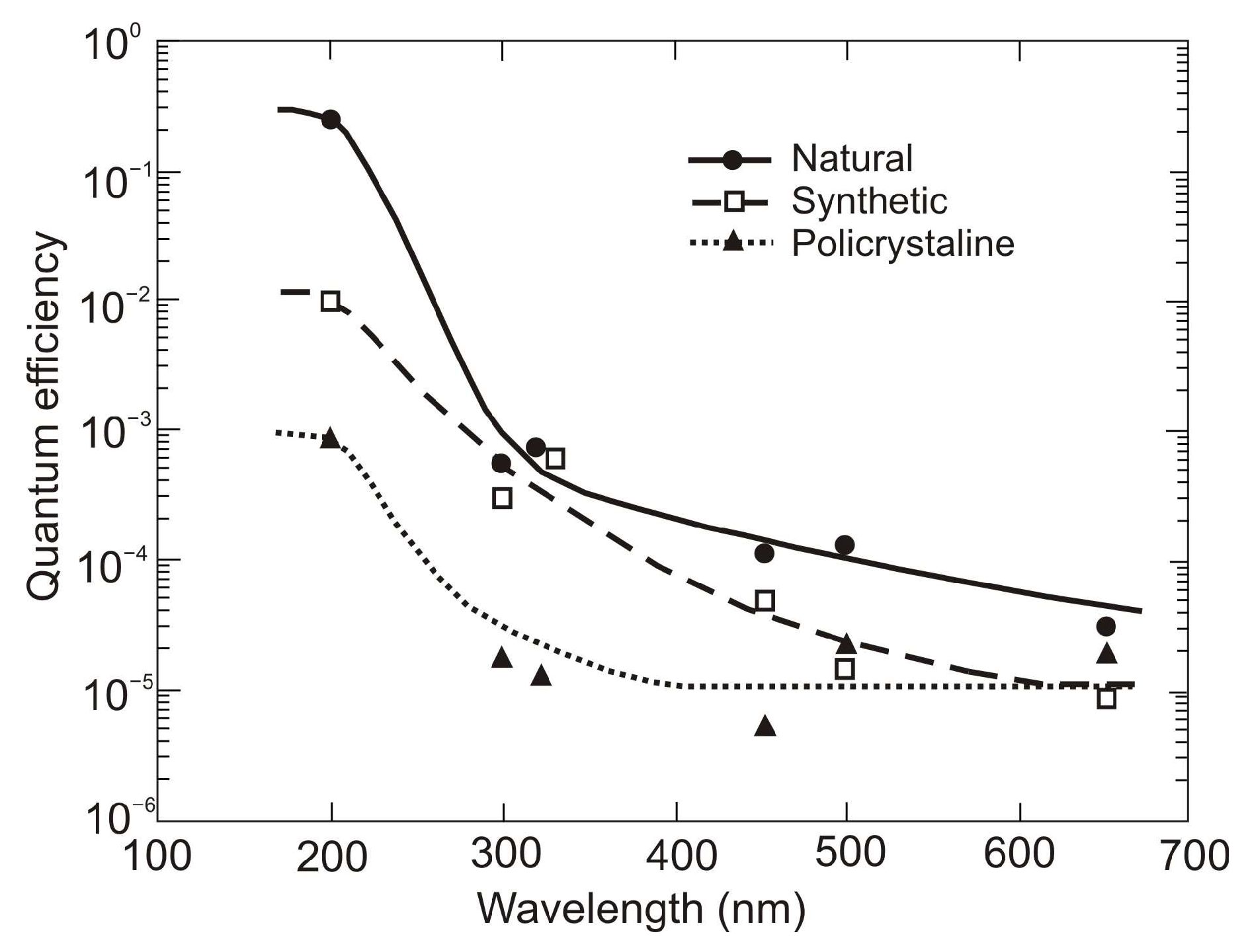
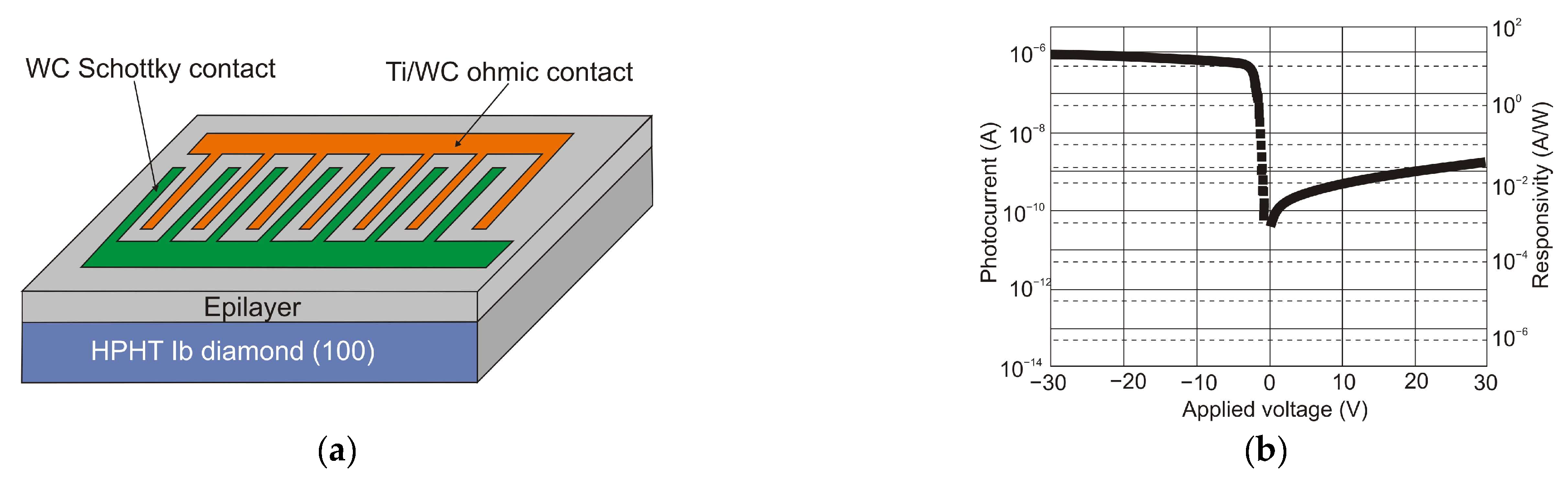
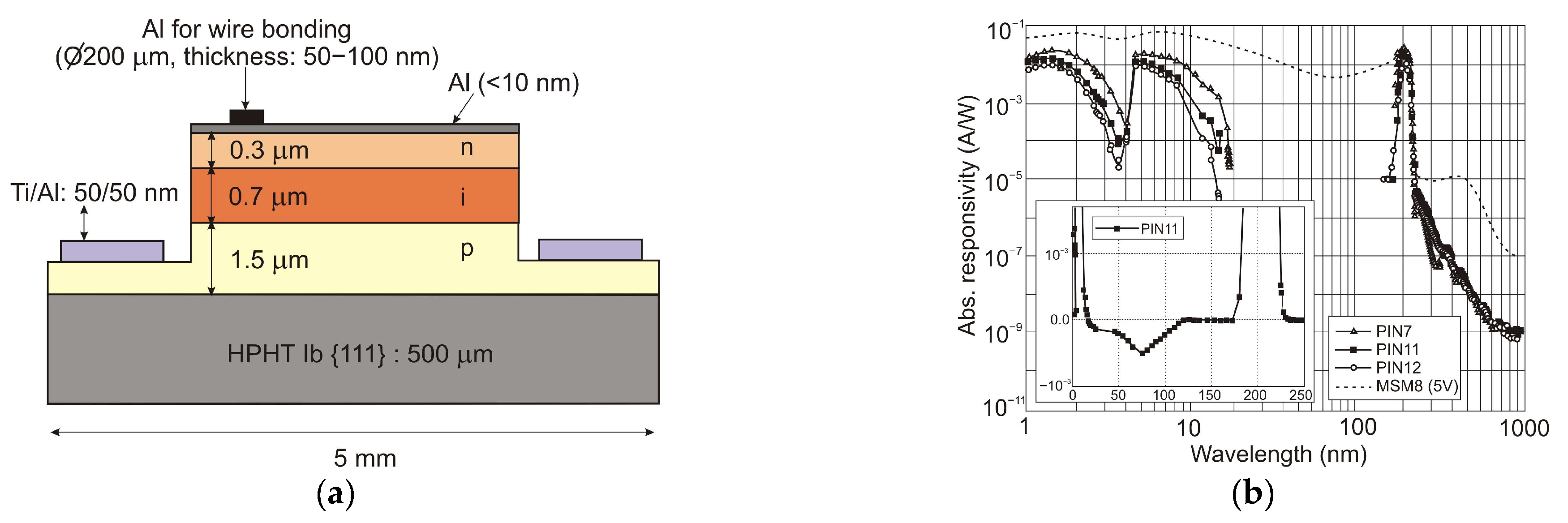
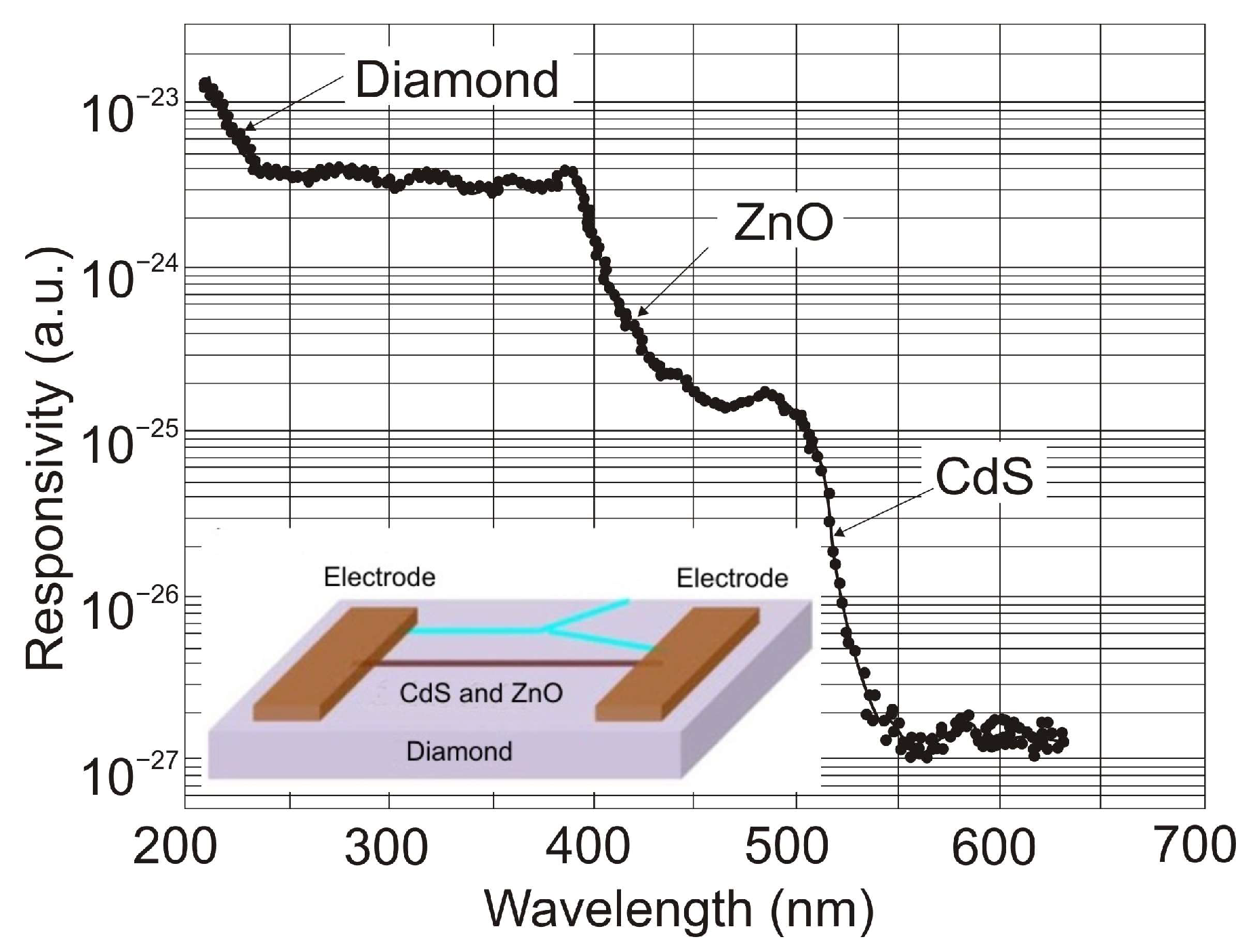
5.3. Diamond-Based Photodetectors
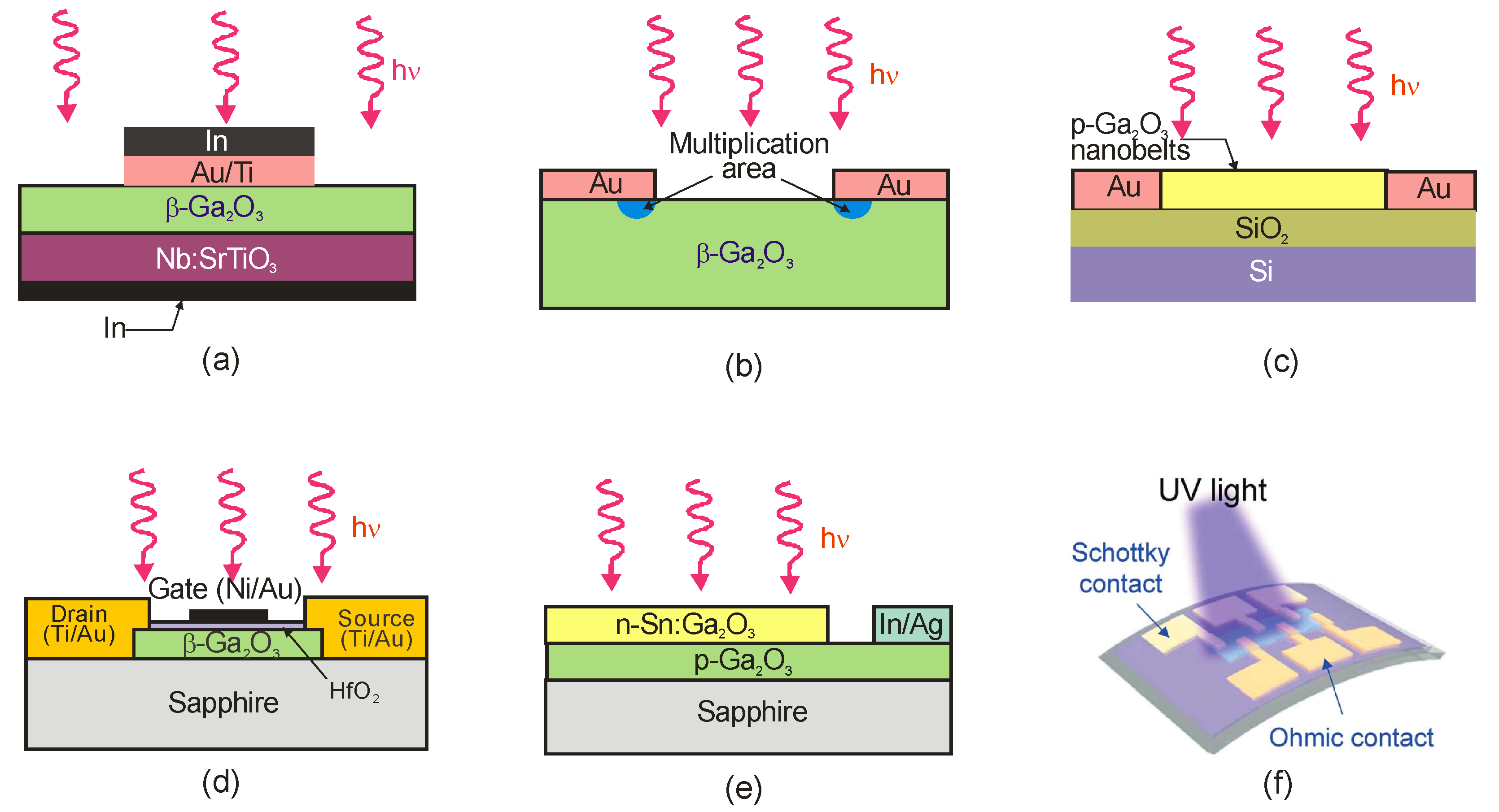
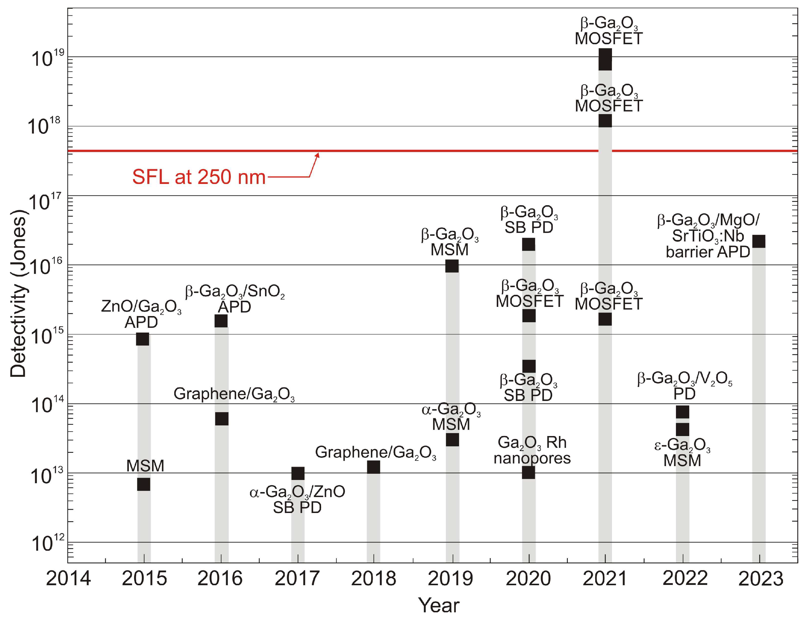
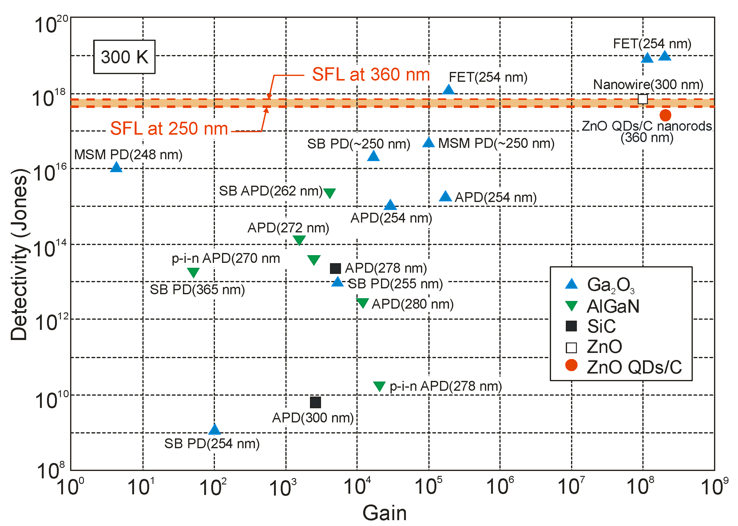
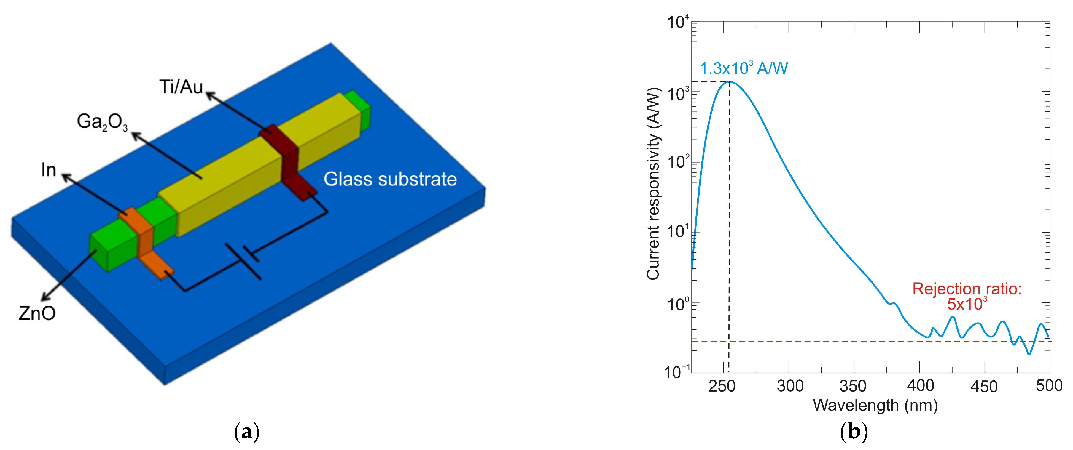
5.4. Ga2O3-Based Photodetectors
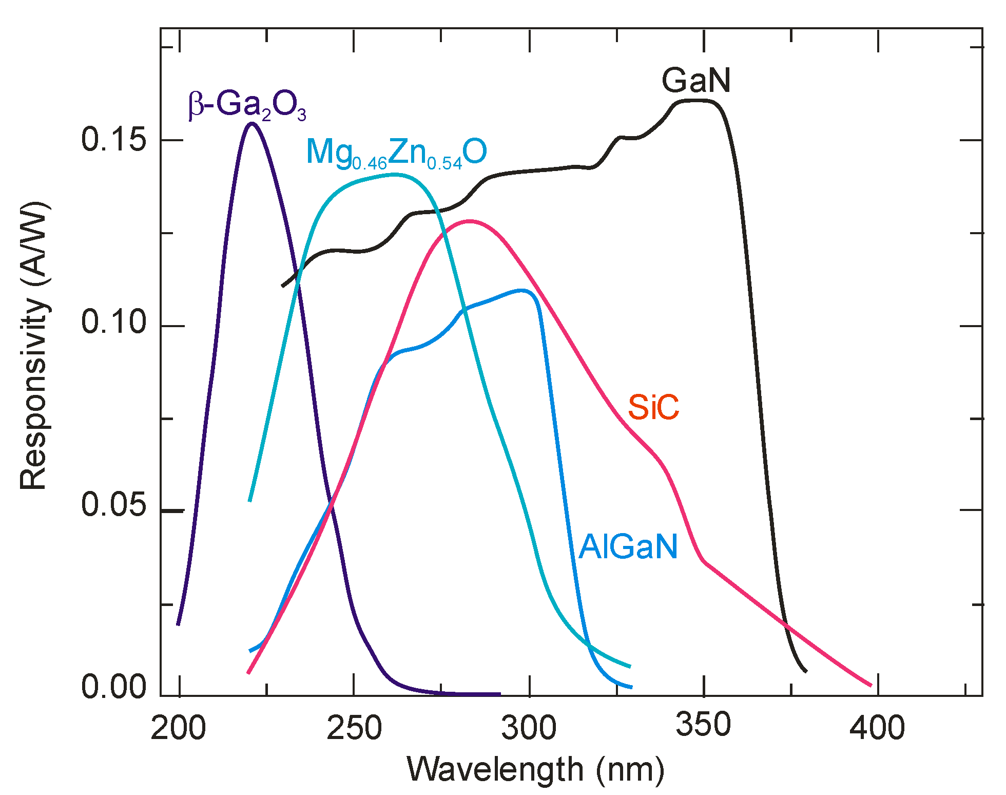
Other Wide Bandgap Photodetectors
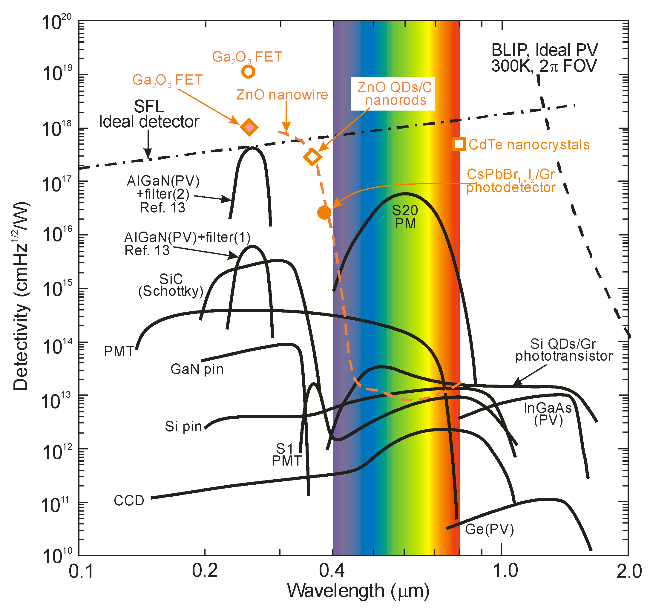
6. New Concepts of UV Photodetectors
- Introduction of various methodologies developed for fabricating semiconductor nanostructures, which can be divided into two categories: top-down (where the dimensional reduction is realized by lithography or patterning techniques) and bottom-up (where the desired nanostructures are built up by individual atoms and molecules) [169];
- Plasmonic enhancement of photodetector performance [170];
- Portable photodetectors based on flexible electronics [175].
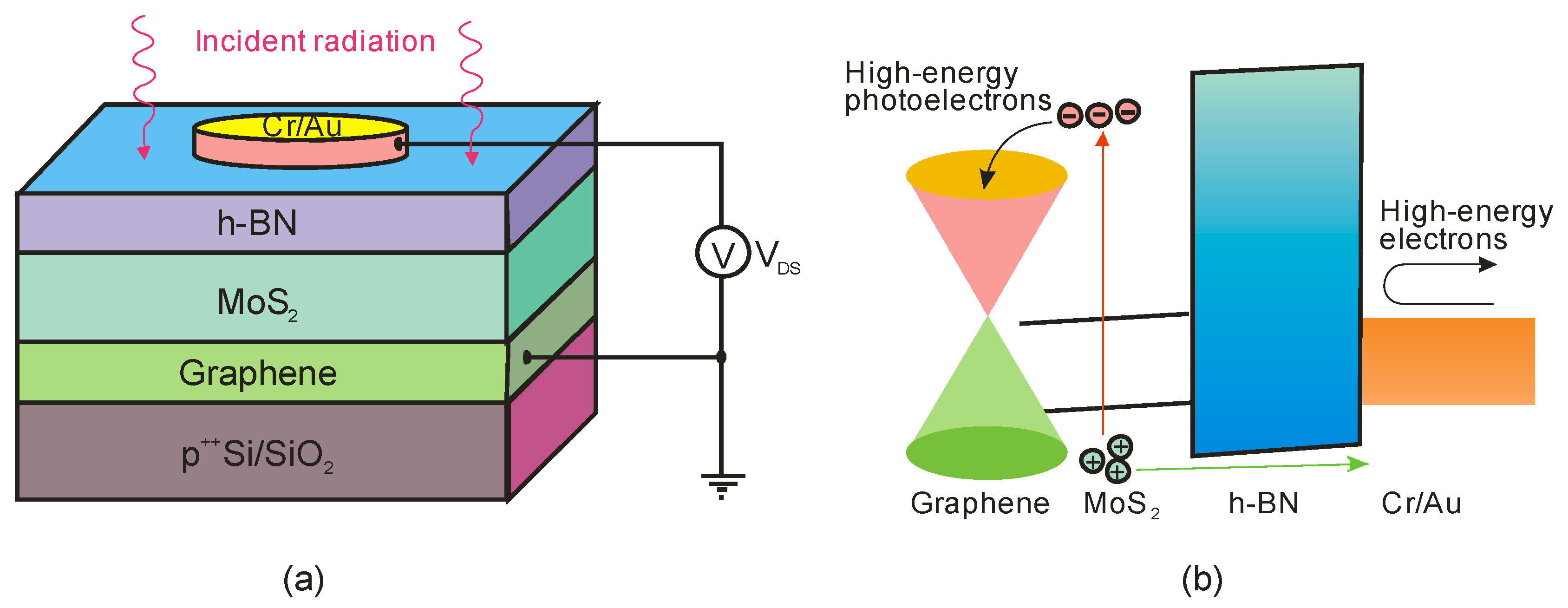
6.1. Low-Dimensional Solid Photodetectors
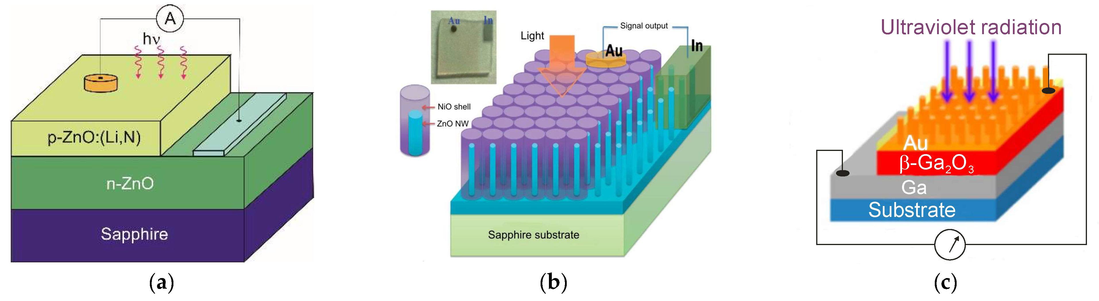
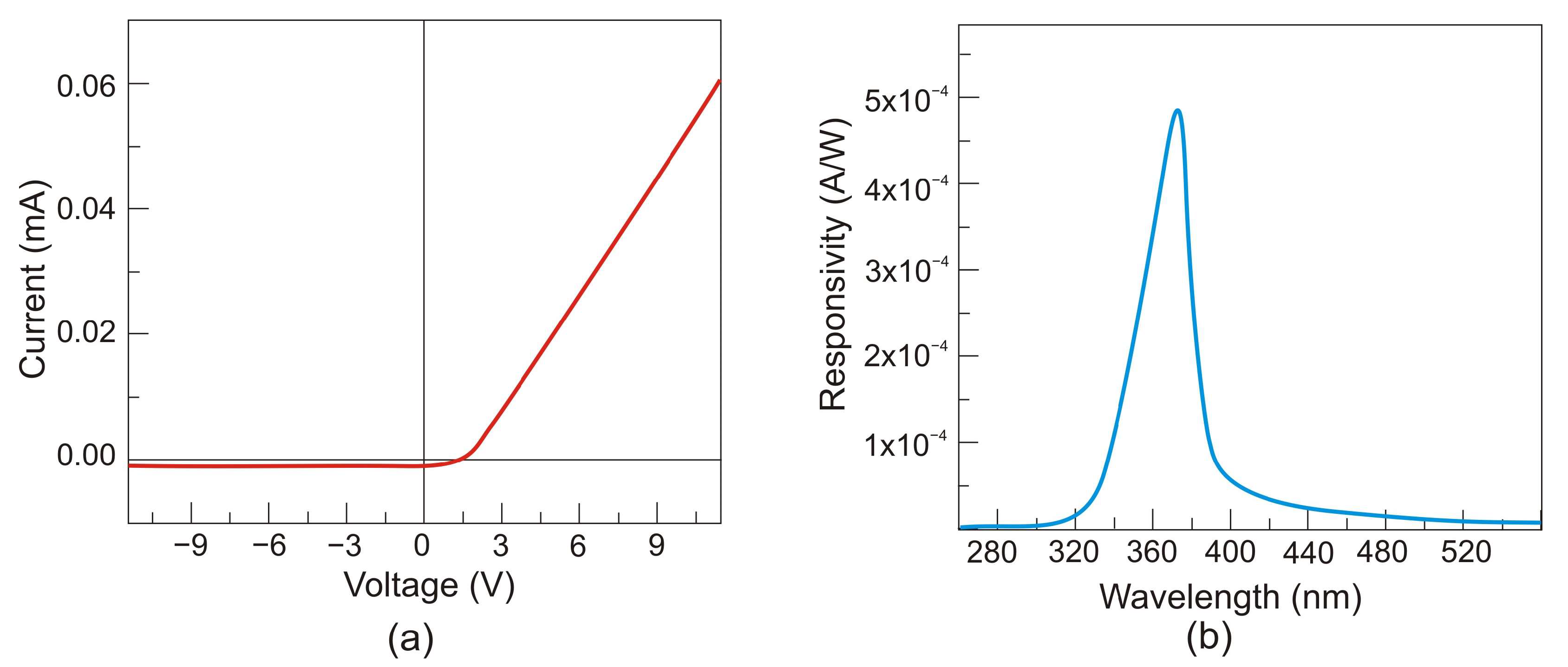
6.2. Self-Powered Photodetectors
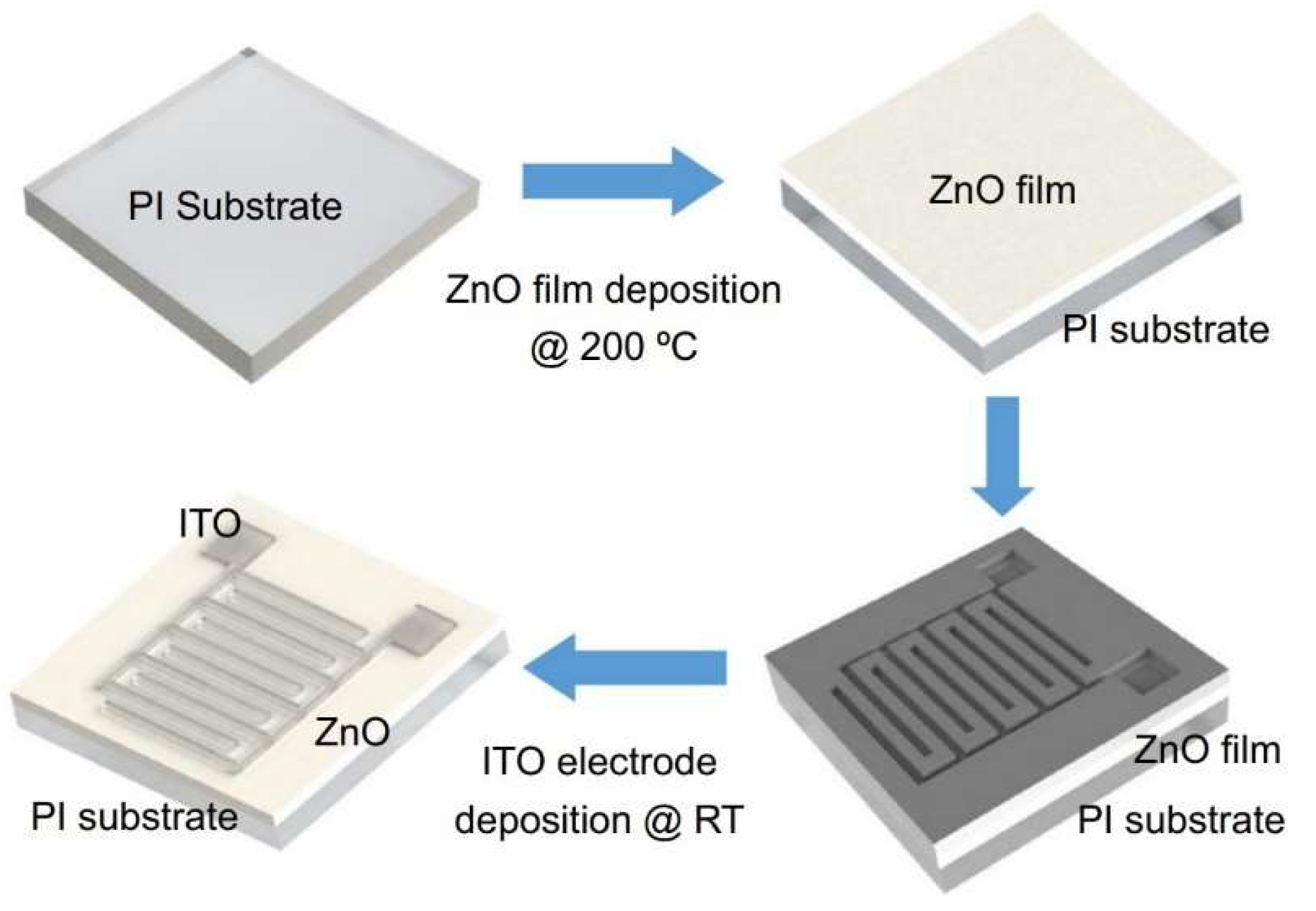
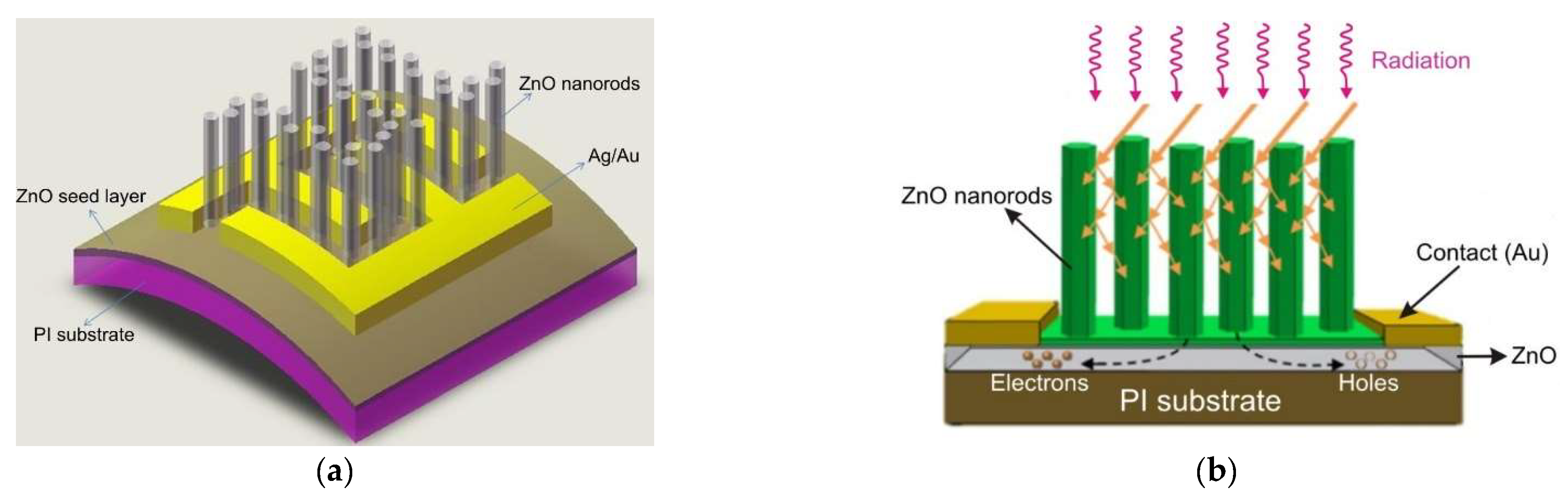
Flexible Photodetectors
7. Conclusions
Author Contributions
Funding
Institutional Review Board Statement
Informed Consent Statement
Data Availability Statement
Conflicts of Interest
References
- Leckner, B. The spectral distribution of solar radiation at the earth’s surface—Elements of a model. Sol. Energy 1978, 20, 143–150. [Google Scholar] [CrossRef]
- International Commission on Non-Ionizing Radiation Protection. Guidelines on limits of exposure to ultraviolet radiation of wavelengths between 180 nm and 400 nm (incoherent optical radiation). Health Phys. 2004, 87, 171–186. [Google Scholar] [CrossRef]
- Commission Internationale de L’Eclairage. Technical Report. Rationalizing Nomenclature for UV Doses and Effects on Humans. CIE 209:2014. WMO/GAW, Raport No. 21, 1-14. Available online: http://files.cie.co.at/724_cie209_2014.pdf (accessed on 29 April 2023).
- The Ozone Hole. Available online: https://www.theozonehole.org/images/uvrayjp.gif (accessed on 22 December 2022).
- Coleman, C.I. Imaging detectors for the ultraviolet. Appl. Opt. 1981, 20, 3693. [Google Scholar] [CrossRef] [PubMed]
- Rogalski, A. Infrared and Terahertz Detectors, 3rd ed.; CRC Press: Boca Raton, FL, USA, 2019; ISBN 9781315271330. [Google Scholar]
- Seib, D.H.; Aukerman, L.W. Photodetectors for the 0.1 to 1.0 μm Spectral Region. Adv. Electron. Electron Phys. 1973, 34, 95–221. [Google Scholar]
- Dereniak, E.L.; Boreman, G.D. Infrared Detectors and Systems; Wiley: New York, NY, USA, 1996; Volume 306, ISBN 978-0-471-12209-8. [Google Scholar]
- Razeghi, M.; Rogalski, A. Semiconductor ultraviolet detectors. J. Appl. Phys. 1996, 79, 7433–7473. [Google Scholar] [CrossRef]
- Kruse, P.W. The Photon Detection Process. In Optical and Infrared Detectors; Springer: Berlin/Heidelberg, Germany, 1977; pp. 5–69. [Google Scholar]
- Boyd, R.W. Radiometry and the Detection of Optical Radiation; Wiley: New York, NY, USA, 1983; ISBN 9780471861881, 047186188X. [Google Scholar]
- Kingston, R.H. Detection of Optical and Infrared Radiation; Springer: Berlin/Heidelberg, Germany, 2013; Volume 10. [Google Scholar]
- Li, X.; Zhu, C.; Zhu, X.; Xu, Z.; Zhuang, X.; Ji, X.; Yan, F. Background limited ultraviolet photodetectors of solar-blind ultraviolet detection. Appl. Phys. Lett. 2013, 103, 171110. [Google Scholar] [CrossRef]
- Koller, L.R. Photoelectric Emission from Thin Films of Caesium. Phys. Rev. 1930, 36, 1639–1647. [Google Scholar] [CrossRef]
- Campbell, N.R., XI. The photoelectric emission of thin films. Lond. Edinb. Dublin Philos. Mag. J. Sci. 1931, 12, 173–185. [Google Scholar] [CrossRef]
- Norton, P.R. Photodetectors. In Handbook of Optics; Bass, M., Van Stryland, E.W., Williams, D.R., Wolfw, W.L., Eds.; McGraw-Hill: New York, NY, USA, 1995; p. 1606. ISBN 0-07-047740-7. [Google Scholar]
- Sembach, K.; Beasley, M.; Blouke, M.; Ebbets, D.; Green, J.; Greer, F.; Jenkins, E.; Joseph, C.; Kimball, R.; MacKenty, J.; et al. Technology Investments to Meet the Needs of Astronomy at Ultraviolet Wavelengths in the 21st Century. Astro2010 Technol. Dev. White Pap. 2009. Available online: https://www.astro.princeton.edu/~dns/Theia/Sembach_UVtechnology_EOS.pdf (accessed on 29 April 2023).
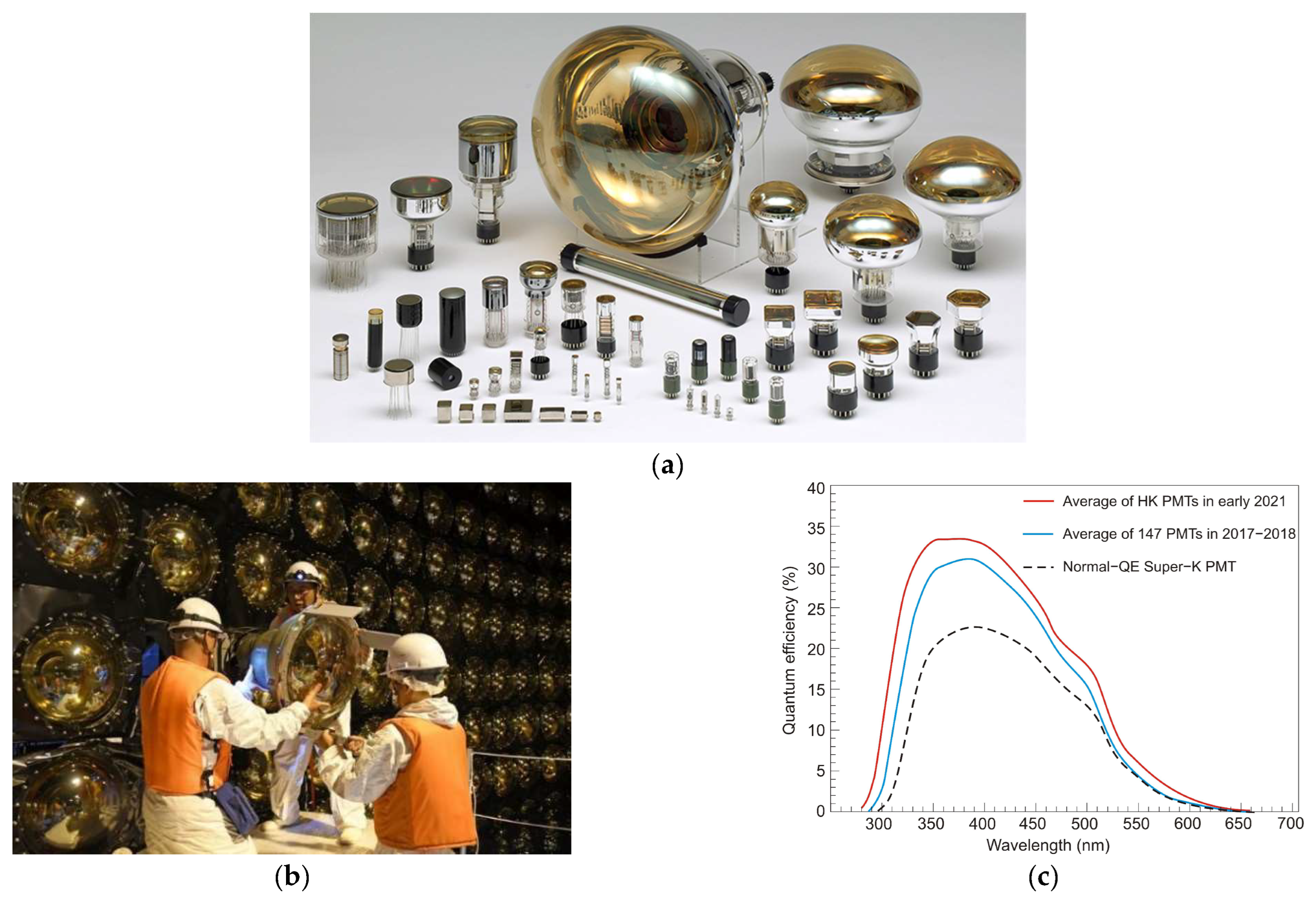
- Hamamatsu Photonics, K.K. Photomultiplier Tubes: Basics and Applications, 4th ed. 2017. Available online: https://www.hamamatsu.com/content/dam/hamamatsu-photonics/sites/documents/99_SALES_LIBRARY/etd/PMT_handbook_v4E.pdf (accessed on 29 April 2023).
- Wallace, J. Photomultiplier tubes do what other photon counters can’t. Laser Focus World 2020, 56, 23–26. [Google Scholar]
- Bronner, C. PMT Development for Hyper-Kamiokande, The 22nd International Workshop on Neutrinos from Accelerators, 2021. Available online: https://indico.cern.ch/event/855372/contributions/4366117/attachments/2303388/3918395/HKPMT_NuFACT.pdf (accessed on 24 April 2023).
- Vallerga, J.; McPhate, J.; Tremsin, A.; Siegmund, O. The current and future capabilities of MCP based UV detectors. Astrophys. Space Sci. 2009, 320, 247–250. [Google Scholar] [CrossRef]
- Conti, L.; Barnstedt, J.; Hanke, L.; Kalkuhl, C.; Kappelmann, N.; Rauch, T.; Stelzer, B.; Werner, K.; Elsener, H.-R.; Schaadt, D.M. MCP detector development for UV space missions. Astrophys. Space Sci. 2018, 363, 63. [Google Scholar] [CrossRef]
- Shi, L.; Nihtianov, S.; Scholze, F.; Gottwald, A.; Nanver, L.K. High-Sensitivity High-Stability Silicon Photodiodes for DUV, VUV and EUV Spectral Ranges. In Proceedings of the SPIE Optical Engineering + Applications, San Diego, CA, USA, 13 September 2011. [Google Scholar] [CrossRef]
- Shi, L.; Nihtianov, S. Comparative Study of Silicon-Based Ultraviolet Photodetectors. IEEE Sens. J. 2012, 12, 2453–2459. [Google Scholar] [CrossRef]
- Nakazawa, T.; Kuroda, R.; Koda, Y.; Sugawa, S. Photodiode Dopant Structure with Atomically Flat Si Surface for High-Sensitivity and Stability to UV Light. Widenhorn, R., Nguyen, V., Dupret, A., Eds.; 2012, p. 82980M. Available online: https://spie.org/Publications/Proceedings/Paper/10.1117/12.907727?SSO=1 (accessed on 26 March 2023).
- Kuroda, R.; Kawada, S.; Nasuno, S.; Nakazawa, T.; Koda, Y.; Hanzawa, K.; Sugawa, S. [Paper] A Highly Ultraviolet Light Sensitive and Highly Robust Image Sensor Technology Based on Flattened Si Surface. ITE Trans. Media Technol. Appl. 2014, 2, 123–130. [Google Scholar] [CrossRef]
- Xia, Z.; Zang, K.; Liu, D.; Zhou, M.; Kim, T.-J.; Zhang, H.; Xue, M.; Park, J.; Morea, M.; Ryu, J.H.; et al. High-sensitivity silicon ultraviolet p+-i-n avalanche photodiode using ultra-shallow boron gradient doping. Appl. Phys. Lett. 2017, 111, 081109. [Google Scholar] [CrossRef]
- Shaw, G.A.; Siegel, A.M.; Model, J.; Geboff, A.; Soloviev, S.; Vert, A.; Sandvik, P. Deep UV Photon-Counting Detectors and Applications. Itzler, M.A., Campbell, J.C., Eds.; 2009, p. 73200J. Available online: https://spie.org/Publications/Proceedings/Paper/10.1117/12.820825 (accessed on 26 March 2023).
- Isoshima, T.; Isojima, Y.; Hakomori, K.; Kikuchi, K.; Nagai, K.; Nakagawa, H. Ultrahigh sensitivity single-photon detector using a Si avalanche photodiode for the measurement of ultraweak biochemiluminescence. Rev. Sci. Instrum. 1995, 66, 2922–2926. [Google Scholar] [CrossRef]
- Si APD, MPPC. Chapter 03. Hamamatsu Catalogue. Available online: https://fdocuments.in/document/si-apd-mppc-chapter-03-1-si-apd-home-si-apd-mppc-chapter-03-2-1-operating.html (accessed on 22 December 2022).
- Ünlü, M.S.; Strite, S. Resonant cavity enhanced photonic devices. J. Appl. Phys. 1995, 78, 607–639. [Google Scholar] [CrossRef]
- El-Batawy, Y.; Mohammedy, F.M.; Deen, M.J. Resonant cavity enhanced photodetectors. In Photodetectors; Elsevier: Amsterdam, The Netherlands, 2016; pp. 415–470. [Google Scholar]
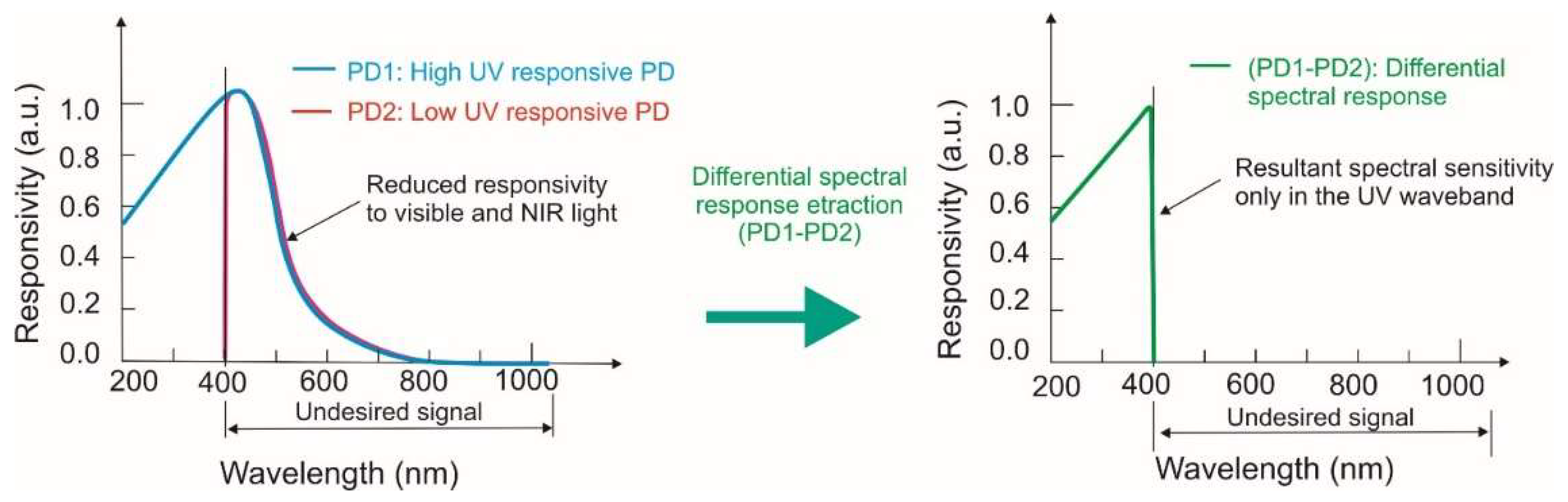
- Sipauba Carvalho da Silva, Y.R.; Koda, Y.; Nasuno, S.; Kuroda, R.; Sugawa, S. An ultraviolet radiation sensor using differential spectral response of silicon photodiodes. In Proceedings of the 2015 IEEE SENSORS, Busan, South Korea, 1–4 November 2015; pp. 1–4. [Google Scholar]
- Sipauba Carvalho da Silva, Y.R.; Kuroda, R.; Sugawa, S. A Highly Robust Silicon Ultraviolet Selective Radiation Sensor Using Differential Spectral Response Method. Sensors 2019, 19, 2755. [Google Scholar] [CrossRef]
- About WFC3. Available online: https://www.stsci.edu/hst/instrumentation/wfc3 (accessed on 22 December 2022).
- BenMoussa, A.; Soltani, A.; Haenen, K.; Kroth, U.; Mortet, V.; Barkad, H.A.; Bolsee, D.; Hermans, C.; Richter, M.; De Jaeger, J.C.; et al. New developments on diamond photodetector for VUV solar observations. Semicond. Sci. Technol. 2008, 23, 035026. [Google Scholar] [CrossRef]
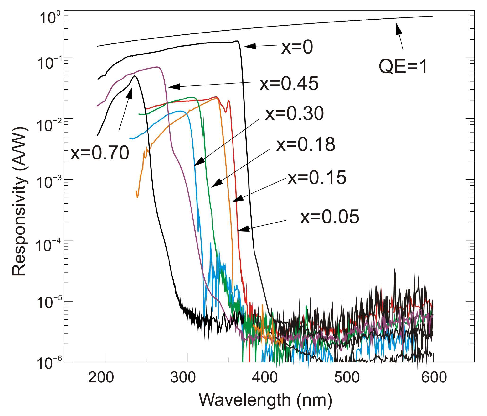
- Misra, M.; Korakakis, D.; Ng, H.M.; Moustakas, T.D. Photoconductive detectors based on partially ordered AlxGa1−xN alloys grown by molecular beam epitaxy. Appl. Phys. Lett. 1999, 74, 2203–2205. [Google Scholar] [CrossRef]
- Carrano, J.C.; Li, T.; Grudowski, P.A.; Eiting, C.J.; Dupuis, R.D.; Campbell, J.C. Comprehensive characterization of metal–semiconductor–metal ultraviolet photodetectors fabricated on single-crystal GaN. J. Appl. Phys. 1998, 83, 6148–6160. [Google Scholar] [CrossRef]
- Walker, D.; Zhang, X.; Kung, P.; Saxler, A.; Javadpour, S.; Xu, J.; Razeghi, M. AlGaN ultraviolet photoconductors grown on sapphire. Appl. Phys. Lett. 1996, 68, 2100–2101. [Google Scholar] [CrossRef]
- Goldenberg, B.; Zook, J.D.; Ulmer, R.J. Fabrication and performance of GaN detectors. In Proceedings of the Topical Workshop on IIIV Nitrides Proc., Nagoya, Japan, 21–23 September 1995. [Google Scholar]
- Kung, P.; Zhang, X.; Walker, D.; Saxler, A.; Piotrowski, J.; Rogalski, A.; Razeghi, M. Kinetics of photoconductivity in n -type GaN photodetector. Appl. Phys. Lett. 1995, 67, 3792–3794. [Google Scholar] [CrossRef]
- Monroy, E.; Calle, F.; Muñoz, E.; Omnès, F.; Beaumont, B.; Gibart, P. Visible-blindness in photoconductive and photovoltaic AlGaN ultraviolet detectors. J. Electron. Mater. 1999, 28, 240–245. [Google Scholar] [CrossRef]
- Xu, W.; Shi, Y.; Ren, F.; Zhou, D.; Su, L.; Liu, Q.; Cheng, L.; Ye, J.; Chen, D.; Zhang, R.; et al. Magnesium ion-implantation-based gallium nitride p-i-n photodiode for visible-blind ultraviolet detection. Photon. Res. 2019, 7, B48. [Google Scholar] [CrossRef]
- Chang, S.; Chang, M.; Yang, Y. Enhanced Responsivity of GaN Metal–Semiconductor–Metal (MSM) Photodetectors on GaN Substrate. IEEE Photon. J. 2017, 9, 1–7. [Google Scholar] [CrossRef]
- Zhao, Y.; Donaldson, W.R. Ultrafast UV AlGaN Metal–Semiconductor–Metal Photodetector with a Response Time Below 25 ps. IEEE J. Quantum Electron. 2020, 56, 1–7. [Google Scholar] [CrossRef]
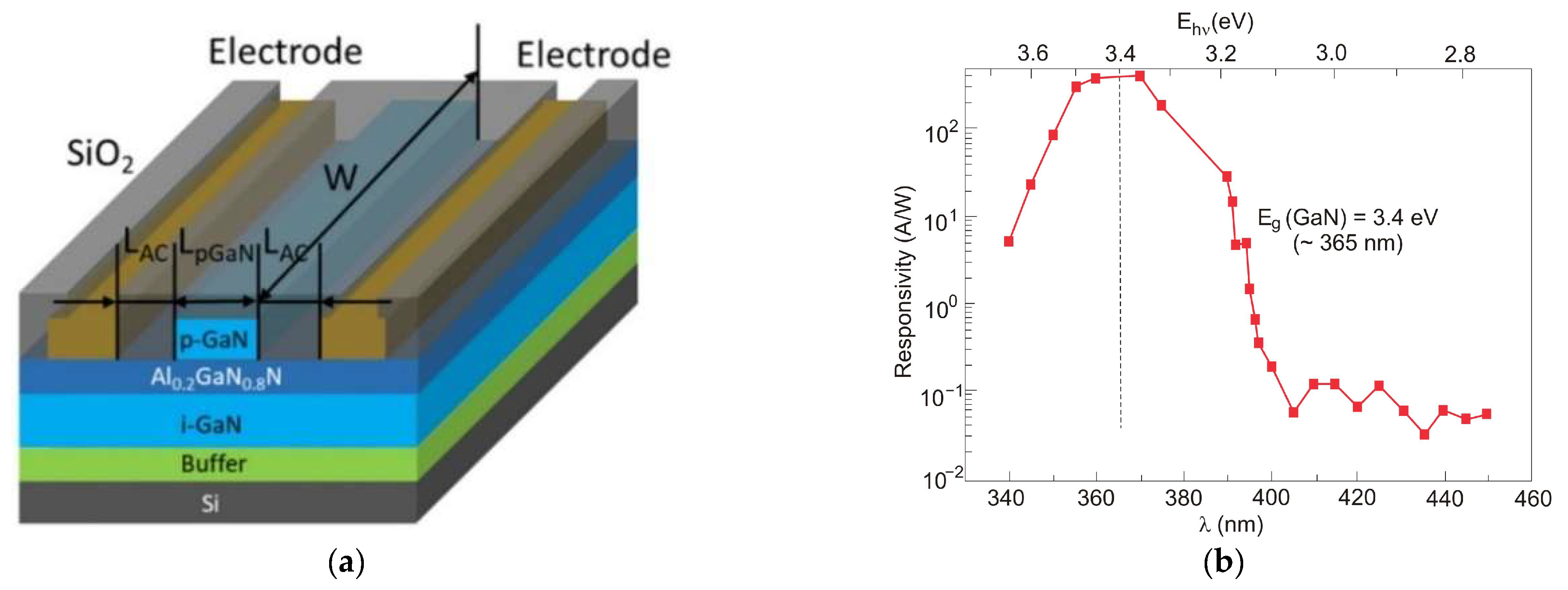
- Lyu, Q.; Jiang, H.; Lau, K.M. High gain and high ultraviolet/visible rejection ratio photodetectors using p-GaN/AlGaN/GaN heterostructures grown on Si. Appl. Phys. Lett. 2020, 117, 071101. [Google Scholar] [CrossRef]
- Zhang, Y.; Shen, S.-C.; Kim, H.J.; Choi, S.; Ryou, J.-H.; Dupuis, R.D.; Narayan, B. Low-noise GaN ultraviolet p-i-n photodiodes on GaN substrates. Appl. Phys. Lett. 2009, 94, 221109. [Google Scholar] [CrossRef]
- Martens, M.; Schlegel, J.; Vogt, P.; Brunner, F.; Lossy, R.; Würfl, J.; Weyers, M.; Kneissl, M. High gain ultraviolet photodetectors based on AlGaN/GaN heterostructures for optical switching. Appl. Phys. Lett. 2011, 98, 211114. [Google Scholar] [CrossRef]
- Li, J.; Zhao, M.; Wang, X.F. High performance Schottky UV photodetectors based on epitaxial AlGaN thin film. Phys. B Condens. Matter 2010, 405, 996–998. [Google Scholar] [CrossRef]
- Muñoz, E. (Al,In,Ga)N-based photodetectors. Some materials issues. Phys. Status Solidi 2007, 244, 2859–2877. [Google Scholar] [CrossRef]
- Chen, Q.; Yang, J.W.; Osinsky, A.; Gangopadhyay, S.; Lim, B.; Anwar, M.Z.; Asif Khan, M.; Kuksenkov, D.; Temkin, H. Schottky barrier detectors on GaN for visible–blind ultraviolet detection. Appl. Phys. Lett. 1997, 70, 2277–2279. [Google Scholar] [CrossRef]
- Bonaccorso, F.; Sun, Z.; Hasan, T.; Ferrari, A.C. Graphene photonics and optoelectronics. Nat. Photon. 2010, 4, 611–622. [Google Scholar] [CrossRef]
- Chang, P.C.; Chen, C.H.; Chang, S.J.; Su, Y.K.; Yu, C.L.; Chen, P.C.; Wang, C.H. AlGaN/GaN MSM photodetectors with photo-CVD annealed Ni/Au semi-transparent contacts. Semicond. Sci. Technol. 2004, 19, 1354–1357. [Google Scholar] [CrossRef]
- Brendel, M.; Helbling, M.; Knigge, A.; Brunner, F.; Weyers, M. Solar-blind AlGaN MSM photodetectors with 24% external quantum efficiency at 0 V. Electron. Lett. 2015, 51, 1598–1600. [Google Scholar] [CrossRef]
- Alaie, Z.; Mohammad Nejad, S.; Yousefi, M.H. Recent advances in ultraviolet photodetectors. Mater. Sci. Semicond. Process. 2015, 29, 16–55. [Google Scholar] [CrossRef]
- Pandit, B.; Cho, J. AlGaN Ultraviolet Metal–Semiconductor–Metal Photodetectors with Reduced Graphene Oxide Contacts. Appl. Sci. 2018, 8, 2098. [Google Scholar] [CrossRef]
- Kishino, K.; Yonemaru, M.; Kikuchi, A.; Toyoura, Y. Resonant-Cavity-Enhanced UV Metal-Semiconductor-Metal (MSM) Photodetectors Based on AlGaN System. Phys. Status Solidi 2001, 188, 321–324. [Google Scholar] [CrossRef]
- Li, D.; Sun, X.; Song, H.; Li, Z.; Chen, Y.; Jiang, H.; Miao, G. Realization of a High-Performance GaN UV Detector by Nanoplasmonic Enhancement. Adv. Mater. 2012, 24, 845–849. [Google Scholar] [CrossRef]
- Sun, X.; Li, D.; Jiang, H.; Li, Z.; Song, H.; Chen, Y.; Miao, G. Improved performance of GaN metal-semiconductor-metal ultraviolet detectors by depositing SiO2 nanoparticles on a GaN surface. Appl. Phys. Lett. 2011, 98, 121117. [Google Scholar] [CrossRef]
- Park, Y.-S. Wide-bandgap III-nitride semiconductors: Opportunities for future optoelectronics. Opto-Electron. Rev. 2001, 9, 117–124. [Google Scholar]
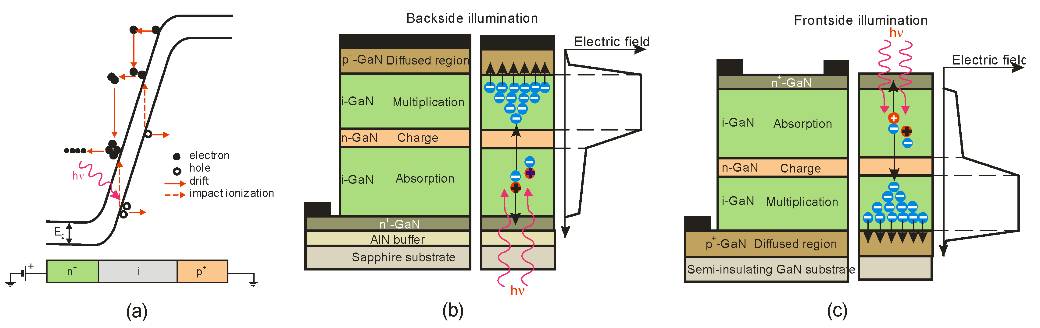
- McClintock, R.; Pau, J.L.; Minder, K.; Bayram, C.; Kung, P.; Razeghi, M. Hole-initiated multiplication in back-illuminated GaN avalanche photodiodes. Appl. Phys. Lett. 2007, 90, 141112. [Google Scholar] [CrossRef]
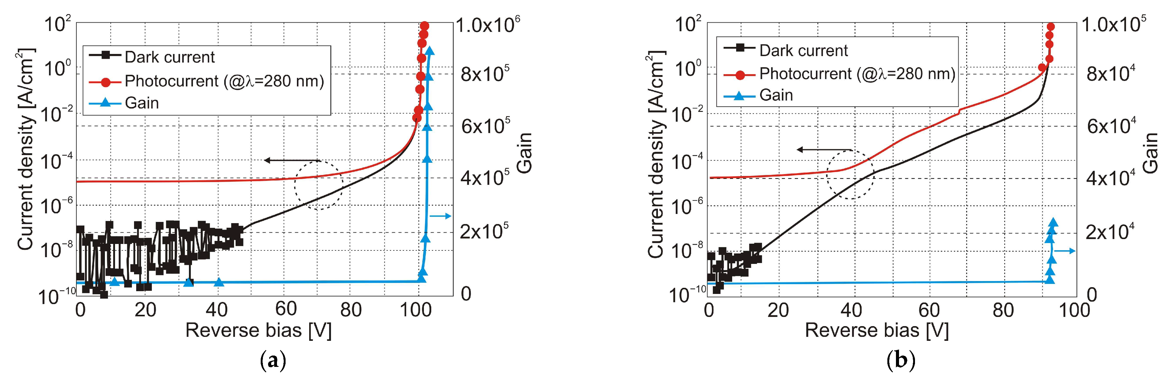
- Ji, D.; Chowdhury, S. On the Scope of GaN-Based Avalanche Photodiodes for Various Ultraviolet-Based Applications. Front. Mater. 2022, 9, 114. [Google Scholar] [CrossRef]
- Ji, D.; Ercan, B.; Benson, G.; Newaz, A.K.M.; Chowdhury, S. 60 A/W high voltage GaN avalanche photodiode demonstrating robust avalanche and high gain up to 525 K. Appl. Phys. Lett. 2020, 116, 211102. [Google Scholar] [CrossRef]
- Bayram, C.; Pau, J.L.; McClintock, R.; Razeghi, M.; Ulmer, M.P.; Silversmith, D. High quantum efficiency back-illuminated GaN avalanche photodiodes. Appl. Phys. Lett. 2008, 93, 211107. [Google Scholar] [CrossRef]
- Cai, Q.; Luo, W.K.; Li, Q.; Li, M.; Chen, D.J.; Lu, H.; Zhang, R.; Zheng, Y.D. AlGaN ultraviolet Avalanche photodiodes based on a triple-mesa structure. Appl. Phys. Lett. 2018, 113, 123503. [Google Scholar] [CrossRef]
- Huang, Y.; Chen, D.J.; Lu, H.; Dong, K.X.; Zhang, R.; Zheng, Y.D.; Li, L.; Li, Z.H. Back-illuminated separate absorption and multiplication AlGaN solar-blind avalanche photodiodes. Appl. Phys. Lett. 2012, 101, 253516. [Google Scholar] [CrossRef]
- Gautam, L.; Jaud, A.G.; Lee, J.; Brown, G.J.; Razeghi, M. Geiger-Mode Operation of AlGaN Avalanche Photodiodes at 255 nm. IEEE J. Quantum Electron. 2021, 57, 1–6. [Google Scholar] [CrossRef]
- Kim, J.; Ji, M.-H.; Detchprohm, T.; Dupuis, R.D.; Ryou, J.-H.; Sood, A.K.; Dhar, N.D.; Lewis, J. Comparison of AlGaN p–i–n ultraviolet avalanche photodiodes grown on free-standing GaN and sapphire substrates. Appl. Phys. Express 2015, 8, 122202. [Google Scholar] [CrossRef]
- Shen, S.C.; Zhang, Y.; Yoo, D.; Limb, J.B.; Ryou, J.H.; Yoder, P.D.; Dupuis, R.D. Performance of Deep Ultraviolet GaN Avalanche Photodiodes Grown by MOCVD. IEEE Photon. Technol. Lett. 2007, 19, 1744–1746. [Google Scholar] [CrossRef]
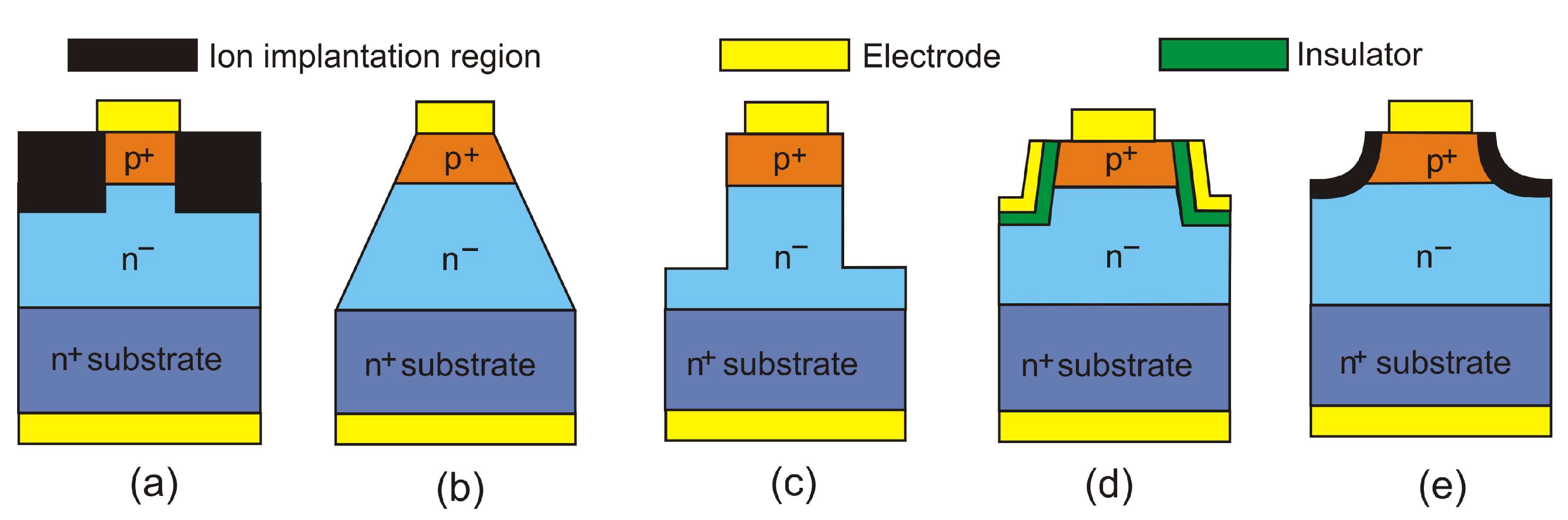
- Wang, W. Uniform and High Gain GaN p-i-n Ultraviolet APDs Enabled by Beveled-Mesa Edge Termination. IEEE Photon. Technol. Lett. 2020, 32, 1357–1360. [Google Scholar] [CrossRef]
- Butun, B.; Tut, T.; Ulker, E.; Yelboga, T.; Ozbay, E. High-performance visible-blind GaN-based p-i-n photodetectors. Appl. Phys. Lett. 2008, 92, 033507. [Google Scholar] [CrossRef]
- Verghese, S.; McIntosh, K.A.; Molnar, R.J.; Mahoney, L.J.; Aggarwal, R.L.; Geis, M.W.; Molvar, K.M.; Duerr, E.K.; Melngailis, I. GaN avalanche photodiodes operating in linear-gain mode and Geiger mode. IEEE Trans. Electron Devices 2001, 48, 502–511. [Google Scholar] [CrossRef]
- Zhou, Q.; McIntosh, D.C.; Lu, Z.; Campbell, J.C.; Sampath, A.V.; Shen, H.; Wraback, M. GaN/SiC avalanche photodiodes. Appl. Phys. Lett. 2011, 99, 131110. [Google Scholar] [CrossRef]
- Carrano, J.C.; Lambert, D.J.H.; Eiting, C.J.; Collins, C.J.; Li, T.; Wang, S.; Yang, B.; Beck, A.L.; Dupuis, R.D.; Campbell, J.C. GaN avalanche photodiodes. Appl. Phys. Lett. 2000, 76, 924–926. [Google Scholar] [CrossRef]
- Sun, L.; Chen, J.; Li, J.; Jiang, H. AlGaN solar-blind avalanche photodiodes with high multiplication gain. Appl. Phys. Lett. 2010, 97, 191103. [Google Scholar] [CrossRef]
- Pau, J.L.; McClintock, R.; Minder, K.; Bayram, C.; Kung, P.; Razeghi, M.; Muñoz, E.; Silversmith, D. Geiger-mode operation of back-illuminated GaN avalanche photodiodes. Appl. Phys. Lett. 2007, 91, 041104. [Google Scholar] [CrossRef]
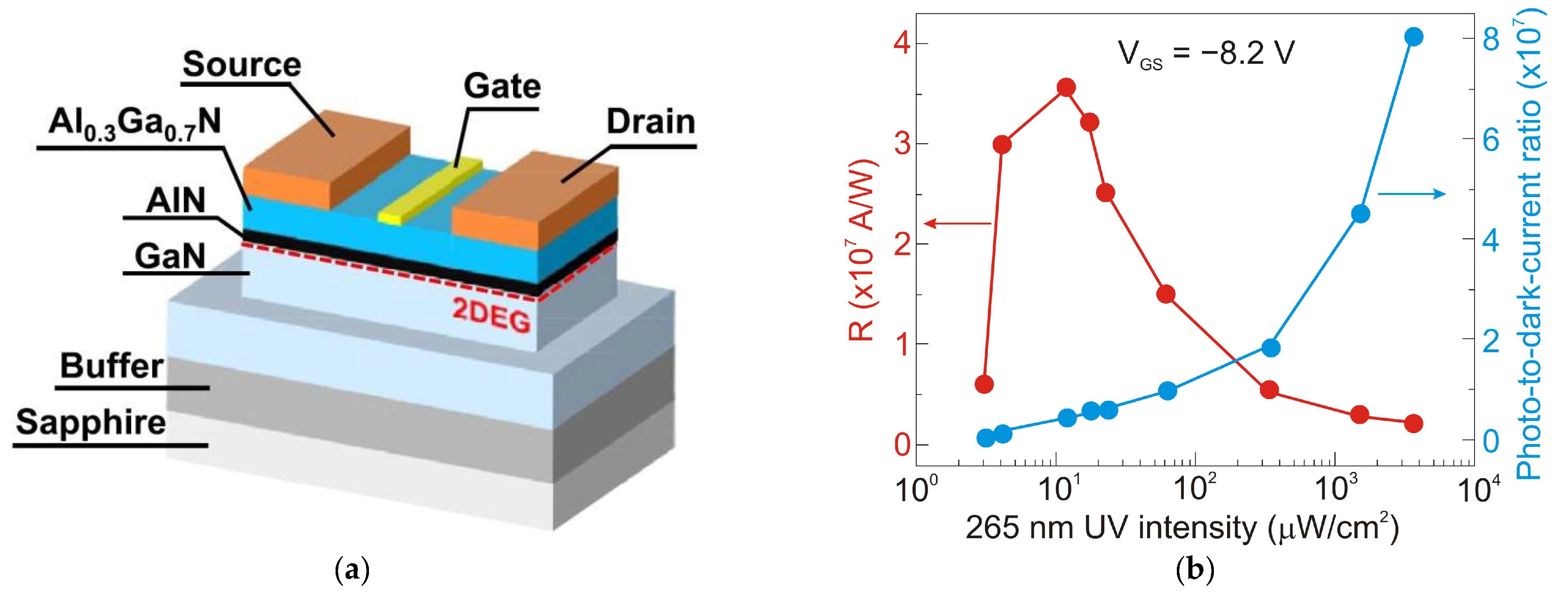
- Zhang, H.; Liang, F.; Song, K.; Xing, C.; Wang, D.; Yu, H.; Huang, C.; Sun, Y.; Yang, L.; Zhao, X.; et al. Demonstration of AlGaN/GaN-based ultraviolet phototransistor with a record high responsivity over 3.6 × 10 7 A/W. Appl. Phys. Lett. 2021, 118, 242105. [Google Scholar] [CrossRef]
- Armstrong, A.M.; Klein, B.; Allerman, A.A.; Douglas, E.A.; Baca, A.G.; Crawford, M.H.; Pickrell, G.W.; Sanchez, C.A. Visible-blind and solar-blind detection induced by defects in AlGaN high electron mobility transistors. J. Appl. Phys. 2018, 123, 114502. [Google Scholar] [CrossRef]
- Malinowski, P.E.; Duboz, J.; De Moor, P.; John, J.; Minoglou, K.; Srivastava, P.; Abdul, H.; Patel, M.; Osman, H.; Semond, F.; et al. Backside illuminated AlGaN-on-Si UV detectors integrated by high density flip-chip bonding. Phys. Status Solidi C 2011, 8, 2476–2478. [Google Scholar] [CrossRef]
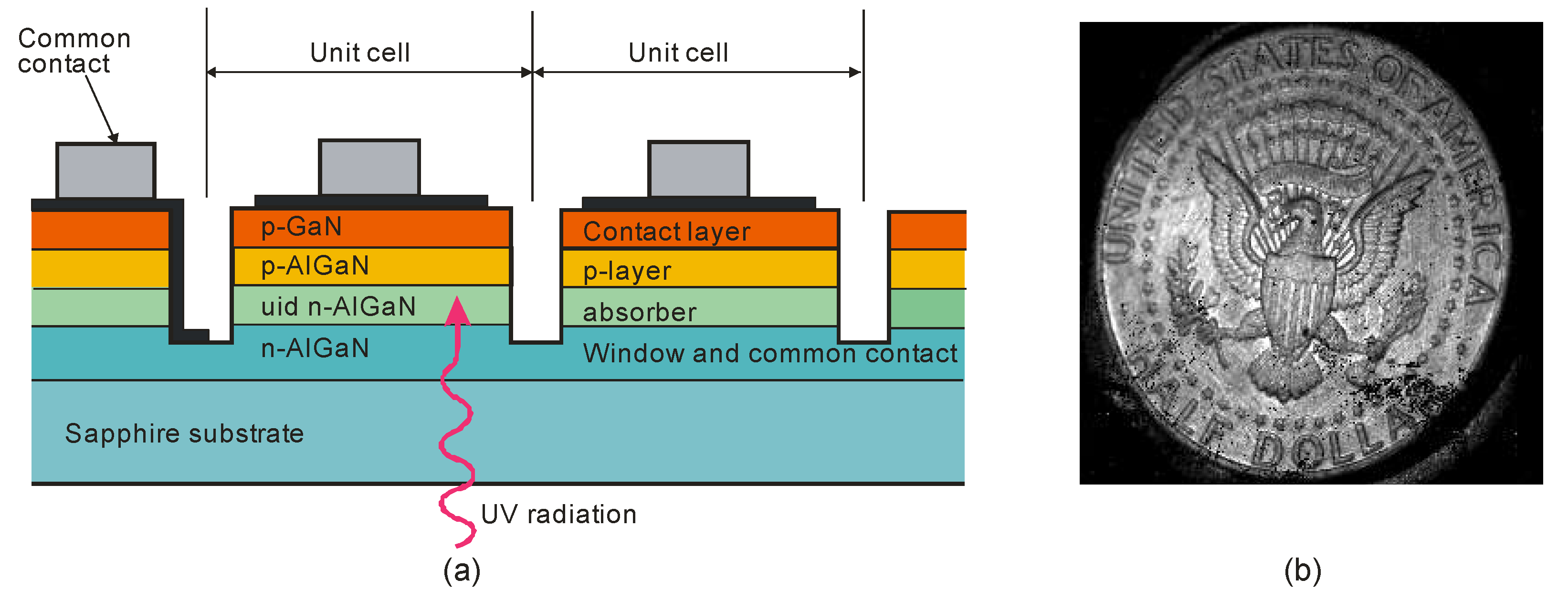
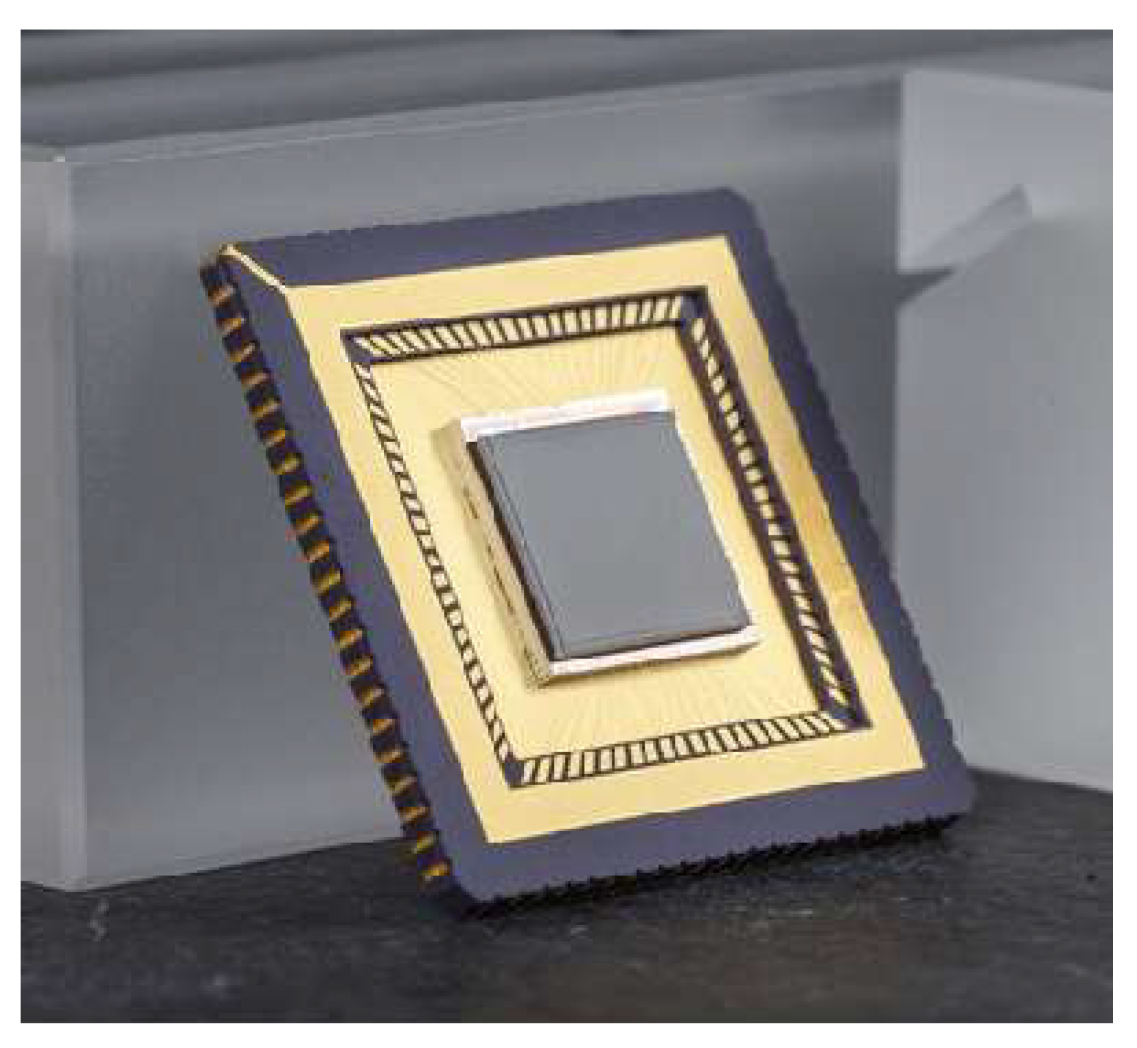
- Cai, Q.; You, H.; Guo, H.; Wang, J.; Liu, B.; Xie, Z.; Chen, D.; Lu, H.; Zheng, Y.; Zhang, R. Progress on AlGaN-based solar-blind ultraviolet photodetectors and focal plane arrays. Light Sci. Appl. 2021, 10, 94. [Google Scholar] [CrossRef] [PubMed]
- Long, J.P.; Varadaraajan, S.; Matthews, J.; Schetzina, J.F. UV detectors and focal plane array imagers based on AlGaN pin photodiodes. Optoelectron. Rev. 2002, 4, 251–260. [Google Scholar]
- McClintock, R.; Mayes, K.; Yasan, A.; Shiell, D.; Kung, P.; Razeghi, M. 320 × 256 solar-blind focal plane arrays based on AlxGa1−xN. Appl. Phys. Lett. 2005, 86, 011117. [Google Scholar] [CrossRef]
- Aslam, S.; Yan, F.; Pugel, D.E.; Franz, D.; Miko, L.; Herrero, F.; Matsumara, M.; Babu, S.; Stahle, C.M. Development of Ultra-High Sensitivity Wide-Band Gap UV-EUV Detectors at NASA Goddard Space Flight Center. In Proceedings of the SPIE Optics and Photonics, San Diego, CA, USA, 18 August 2005. [Google Scholar] [CrossRef]
- Reine, M.B.; Hairston, A.; Lamarre, P.; Wong, K.K.; Tobin, S.P.; Sood, A.K.; Cooke, C.; Pophristic, M.; Guo, S.; Peres, B.; et al. Solar-Blind AlGaN 256 × 256 p-i-n Detectors and Focal Plane Arrays. Litton, C.W., Grote, J.G., Morkoc, H., Madhukar, A., Eds.; 2006, p. 61210R. Available online: https://www.spiedigitallibrary.org/conference-proceedings-of-spie/6121/61210R/Solar-blind-AlGaN-256256-p-i-n-detectors-and-focal/10.1117/12.654793.short (accessed on 26 March 2023).
- Reverchon, J.-L.; Robo, J.-A.; Truffer, J.-P.; Caumes, J.-P.; Mourad, I.; Brault, J.; Duboz, J.-Y. AlGaN-Based Focal Plane Arrays for Selective UV Imaging at 310 nm and 280 nm and Route toward Deep UV Imaging. Meynart, R., Neeck, S.P., Shimoda, H., Habib, S., Eds.; 2007, p. 674417. Available online: https://ui.adsabs.harvard.edu/abs/2007SPIE.6744E..17R/abstract (accessed on 26 March 2023).
- Yuan, Y.; Zhang, Y.; Chu, K.; Li, X.; Zhao, D.; Yang, H. Development of solar-blind AlGaN 128 × 128 Ultraviolet Focal Plane Arrays. Sci. China Ser. E Technol. Sci. 2008, 51, 820–826. [Google Scholar] [CrossRef]
- Duboz, J.; Brault, J.; Truffer, J.; Robot, J.; Robin, K.; Reverchon, J.L. UV imaging based on AlGaN arrays. Phys. Status Solidi C 2009, 6, S611–S614. [Google Scholar] [CrossRef]
- Malinowski, P.E.; Duboz, J.-Y.; De Moor, P.; John, J.; Minoglou, K.; Srivastava, P.; Semond, F.; Frayssinet, E.; Giordanengo, B.; BenMoussa, A.; et al. AlGaN-on-Si-based 10-μm pixel-to-pixel pitch hybrid imagers for the EUV range. IEEE Electron Device Lett. 2011, 32, 1561–1563. [Google Scholar] [CrossRef]
- Cicek, E.; McClintock, R.; Cho, C.Y.; Rahnema, B.; Razeghi, M. Al x Ga 1−x N-based solar-blind ultraviolet photodetector based on lateral epitaxial overgrowth of AlN on Si substrate. Appl. Phys. Lett. 2013, 103, 181113. [Google Scholar] [CrossRef]
- McClintock, R.; Razeghi, M. Solar-Blind Photodetectors and Focal Plane Arrays Based on AlGaN. Razeghi, M., Temple, D.S., Brown, G.J., Eds.; 2015, p. 955502. Available online: https://www.spiedigitallibrary.org/conference-proceedings-of-spie/9555/955502/Solar-blind-photodetectors-and-focal-plane-arrays-based-on-AlGaN/10.1117/12.2195390.short (accessed on 26 March 2023).
- Rehm, R.; Driad, R.; Kirste, L.; Leone, S.; Passow, T.; Rutz, F.; Watschke, L.; Zibold, A. Toward AlGaN Focal Plane Arrays for Solar-Blind Ultraviolet Detection. Phys. Status Solidi 2020, 217, 1900769. [Google Scholar] [CrossRef]
- Aldalbahi, A.; Li, E.; Rivera, M.; Velazquez, R.; Altalhi, T.; Peng, X.; Feng, P.X. A new approach for fabrications of SiC based photodetectors. Sci. Rep. 2016, 6, 23457. [Google Scholar] [CrossRef]
- Chen, Y.; Wu, L.; Sun, W.; Lu, Y.; Huang, Z. High temperature phase equilibrium of SiC-based ceramic systems. In Properties and Applications of Silicon Carbide; Gerhardt, R., Ed.; InTech: Rijeka, Croatia, 2011; pp. 445–446. ISBN 978-953-307-201-2. [Google Scholar]
- Monroy, E.; Omns, F.; Calle, F. Wide-bandgap semiconductor ultraviolet photodetectors. Semicond. Sci. Technol. 2003, 18, R33–R51. [Google Scholar] [CrossRef]
- Seely, J.F.; Kjornrattanawanich, B.; Holland, G.E.; Korde, R. Response of a SiC photodiode to extreme ultraviolet through visible radiation. Opt. Lett. 2005, 30, 3120. [Google Scholar] [CrossRef] [PubMed]
- Mazzillo, M.; Sciuto, A.; Mannino, G.; Renna, L.; Costa, N.; Badalà, P. Towards a high performing UV-A sensor based on Silicon Carbide and hydrogenated Silicon Nitride absorbing layers. J. Instrum. 2016, 11, P10010. [Google Scholar] [CrossRef]
- Mazzillo, M.; Shukla, P.; Mallik, R.; Kumar, M.; Previti, R.; Di Marco, G.; Sciuto, A.; Puglisi, R.A.; Raineri, V. 4H-SiC Schottky Photodiode Based Demonstrator Board for UV-Index Monitoring. IEEE Sens. J. 2011, 11, 377–381. [Google Scholar] [CrossRef]
- Kestle, A.; Wilks, S.P.; Dunstan, P.R.; Pritchard, M.; Mawby, P.A. Improved Ni/SiC Schottky diode formation. Electron. Lett. 2000, 36, 267. [Google Scholar] [CrossRef]
- Defives, D.; Noblanc, O.; Dua, C.; Brylinski, C.; Barthula, M.; Meyer, F. Electrical characterization of inhomogeneous Ti/4H–SiC Schottky contacts. Mater. Sci. Eng. B 1999, 61–62, 395–401. [Google Scholar] [CrossRef]
- Su, Y.-K.; Chiou, Y.-Z.; Chang, C.-S.; Chang, S.-J.; Lin, Y.-C.; Chen, J.F. 4H-SiC metal–semiconductor–metal ultraviolet photodetectors with Ni/ITO electrodes. Solid-State Electron. 2002, 46, 2237–2240. [Google Scholar] [CrossRef]
- Lien, W.-C.; Tsai, D.-S.; Lien, D.-H.; Senesky, D.G.; He, J.-H.; Pisano, A.P. 4H-SiC metal-semiconductor-metal ultraviolet photodetectors in operation of 450C. IEEE Electron Device Lett. 2012, 33, 1586–1588. [Google Scholar] [CrossRef]
- Zhang, F.; Yang, W.; Huang, H.; Chen, X.; Wu, Z.; Zhu, H.; Qi, H.; Yao, J.; Fan, Z.; Shao, J. High-performance 4H-SiC based metal-semiconductor-metal ultraviolet photodetectors with Al2O3∕SiO2 films. Appl. Phys. Lett. 2008, 92, 251102. [Google Scholar] [CrossRef]
- Yang, W.; Zhang, F.; Liu, Z.; Wu, Z. Effects of annealing on the performance of 4H-SiC metal–semiconductor–metal ultraviolet photodetectors. Mater. Sci. Semicond. Process. 2008, 11, 59–62. [Google Scholar] [CrossRef]
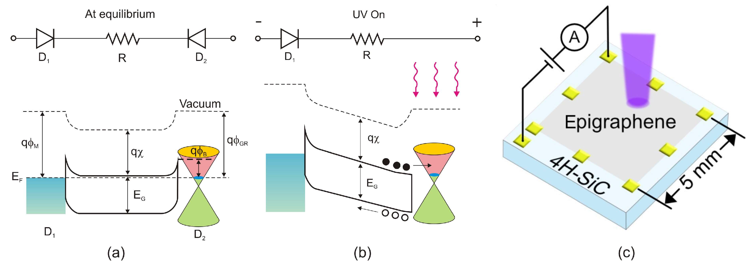
- He, H.; Shetty, N.; Kubatkin, S.; Stadler, P.; Löfwander, T.; Fogelström, M.; Miranda-Valenzuela, J.C.; Yakimova, R.; Bauch, T.; Lara-Avila, S. Highly efficient UV detection in a metal–semiconductor–metal detector with epigraphene. Appl. Phys. Lett. 2022, 120, 191101. [Google Scholar] [CrossRef]
- Cai, J.; Chen, X.; Hong, R.; Yang, W.; Wu, Z. High-performance 4H-SiC-based p-i-n ultraviolet photodiode and investigation of its capacitance characteristics. Opt. Commun. 2014, 333, 182–186. [Google Scholar] [CrossRef]
- Sciuto, A.; Mazzillo, M.C.; Di Franco, S.; Mannino, G.; Badala, P.; Renna, L.; Caruso, C. UV-A Sensor Based on 6H-SiC Schottky Photodiode. IEEE Photon. J. 2017, 9, 1–10. [Google Scholar] [CrossRef]
- Lioliou, G.; Mazzillo, M.C.; Sciuto, A.; Barnett, A.M. Electrical and ultraviolet characterization of 4H-SiC Schottky photodiodes. Opt. Express 2015, 23, 21657. [Google Scholar] [CrossRef] [PubMed]
- Mazzillo, M.; Sciuto, A.; Marchese, S. Electro-Optical Characterization of Patterned Thin Metal Film Ni2Si–4H SiC Schottky Photodiodes for Ultraviolet Light Detection. IEEE Sens. J. 2015, 15, 1858–1863. [Google Scholar] [CrossRef]
- Xu, Y.; Zhou, D.; Lu, H.; Chen, D.; Ren, F.; Zhang, R.; Zheng, Y. High-temperature and reliability performance of 4H-SiC Schottky-barrier photodiodes for UV detection. J. Vac. Sci. Technol. B Nanotechnol. Microelectron. Mater. Process. Meas. Phenom. 2015, 33, 040602. [Google Scholar] [CrossRef]
- Chen, X.; Zhu, H.; Cai, J.; Wu, Z. High-performance 4H-SiC-based ultraviolet p-i-n photodetector. J. Appl. Phys. 2007, 102, 024505. [Google Scholar] [CrossRef]
- Megherbi, M.L.; Bencherif, H.; Dehimi, L.; Mallemace, E.D.; Rao, S.; Pezzimenti, F.; Della Corte, F.G. An Efficient 4H-SiC Photodiode for UV Sensing Applications. Electronics 2021, 10, 2517. [Google Scholar] [CrossRef]
- Liu, H.-D.; Guo, X.; McIntosh, D.; Campbell, J.C. Demonstration of Ultraviolet 6H-SiC PIN Avalanche Photodiodes. IEEE Photon. Technol. Lett. 2006, 18, 2508–2510. [Google Scholar] [CrossRef]
- Cai, X.; Zhou, D.; Yang, S.; Lu, H.; Chen, D.; Ren, F.; Zhang, R.; Zheng, Y. 4H-SiC SACM Avalanche Photodiode with Low Breakdown Voltage and High UV Detection Efficiency. IEEE Photon. J. 2016, 8, 1–7. [Google Scholar] [CrossRef]
- Bai, X.; Guo, X.; Mcintosh, D.C.; Liu, H.-D.; Campbell, J.C. High Detection Sensitivity of Ultraviolet 4H-SiC Avalanche Photodiodes. IEEE J. Quantum Electron. 2007, 43, 1159–1162. [Google Scholar] [CrossRef]
- Zhu, H.; Chen, X.; Cai, J.; Wu, Z. 4H–SiC ultraviolet avalanche photodetectors with low breakdown voltage and high gain. Solid-State Electron. 2009, 53, 7–10. [Google Scholar] [CrossRef]
- Sciuto, A.; Mazzillo, M.; Lenzi, P.; Di Franco, S.; Mello, D.; Barbarino, P.P.; Longo, G.; Cascino, S.; Santangelo, A.; Albergo, S.; et al. Fully Planar 4H-SiC Avalanche Photodiode with Low Breakdown Voltage. IEEE Sens. J. 2017, 17, 4460–4465. [Google Scholar] [CrossRef]
- Zhou, X.; Han, T.; Lv, Y.; Li, J.; Lu, W.; Wang, Y.; Song, X.; Tan, X.; Liang, S.; Feng, Z.; et al. Large-Area 4H-SiC Ultraviolet Avalanche Photodiodes Based on Variable-Temperature Reflow Technique. IEEE Electron Device Lett. 2018, 39, 1724–1727. [Google Scholar] [CrossRef]
- Zhou, D.; Liu, F.; Lu, H.; Chen, D.; Ren, F.; Zhang, R.; Zheng, Y. High-Temperature Single Photon Detection Performance of 4H-SiC Avalanche Photodiodes. IEEE Photon. Technol. Lett. 2014, 26, 1136–1138. [Google Scholar] [CrossRef]
- Li, L.; Zhou, D.; Lu, H.; Liu, W.; Mo, X.; Ren, F.; Chen, D.; Wang, R.; Li, G.; Zhang, R.; et al. 4H–SiC Avalanche Photodiode Linear Array Operating in Geiger Mode. IEEE Photon. J. 2017, 9, 1–7. [Google Scholar] [CrossRef]
- Xin, X.; Yan, F.; Sun, X.; Alexandrove, P.; Stahle, C.M.; Hu, J.; Matsumura, M.; Li, X.; Weiner, M.; Zhao, H.J. Demonstration of 4H-SiC UV single photon counting avalanche photodiode. Electron. Lett. 2005, 41, 1. [Google Scholar] [CrossRef]
- Beck, A.L.; Karve, G.; Wang, S.; Ming, J.; Guo, X.; Campbell, J.C. Geiger mode operation of ultraviolet 4H-SiC avalanche photodiodes. IEEE Photon. Technol. Lett. 2005, 17, 1507–1509. [Google Scholar] [CrossRef]
- Omnès, F.; Monroy, E.; Muñoz, E.; Reverchon, J.-L. Wide Bandgap UV Photodetectors: A Short Review of Devices and Applications. In Proceedings of the SPIE Integrated Optoelectronic Devices, San Jose, CA, USA, 8 February 2007. [Google Scholar] [CrossRef]
- Umezawa, H. Recent advances in diamond power semiconductor devices. Mater. Sci. Semicond. Process. 2018, 78, 147–156. [Google Scholar] [CrossRef]
- Wort, C.J.H.; Balmer, R.S. Diamond as an electronic material. Mater. Today 2008, 11, 22–28. [Google Scholar] [CrossRef]
- Lu, Y.-J.; Lin, C.-N.; Shan, C.-X. Optoelectronic Diamond: Growth, Properties, and Photodetection Applications. Adv. Opt. Mater. 2018, 6, 1800359. [Google Scholar] [CrossRef]
- Liao, M. Progress in semiconductor diamond photodetectors and MEMS sensors. Funct. Diam. 2021, 1, 29–46. [Google Scholar] [CrossRef]
- Liao, M.; Koide, Y. High-performance metal-semiconductor-metal deep-ultraviolet photodetectors based on homoepitaxial diamond thin film. Appl. Phys. Lett. 2006, 89, 113509. [Google Scholar] [CrossRef]
- Mihailetchi, V.D.; Wildeman, J.; Blom, P.W.M. Space-Charge Limited Photocurrent. Phys. Rev. Lett. 2005, 94, 126602. [Google Scholar] [CrossRef]
- Lin, C.-N.; Lu, Y.-J.; Yang, X.; Tian, Y.-Z.; Gao, C.-J.; Sun, J.-L.; Dong, L.; Zhong, F.; Hu, W.-D.; Shan, C.-X. Diamond-Based All-Carbon Photodetectors for Solar-Blind Imaging. Adv. Opt. Mater. 2018, 6, 1800068. [Google Scholar] [CrossRef]
- Binari, S.C.; Marchywka, M.; Koolbeck, D.A.; Dietrich, H.B.; Moses, D. Diamond metal-semiconductor-metal ultraviolet photodetectors. Diam. Relat. Mater. 1993, 2, 1020–1023. [Google Scholar] [CrossRef]
- Dominik, M.; Koba, M.; Bogdanowicz, R.; Bock, W.J.; Śmietana, M. Plasma-Based Deposition and Processing Techniques for Optical Fiber Sensing. 2017, pp. 95–114. Available online: https://link.springer.com/chapter/10.1007/978-3-319-42625-9_5 (accessed on 26 March 2023).
- Balducci, A.; Marinelli, M.; Milani, E.; Morgada, M.E.; Tucciarone, A.; Verona-Rinati, G.; Angelone, M.; Pillon, M. Extreme ultraviolet single-crystal diamond detectors by chemical vapor deposition. Appl. Phys. Lett. 2005, 86, 193509. [Google Scholar] [CrossRef]
- Alvarez, J.; Liao, M.; Koide, Y. Large deep-ultraviolet photocurrent in metal-semiconductor-metal structures fabricated on as-grown boron-doped diamond. Appl. Phys. Lett. 2005, 87, 113507. [Google Scholar] [CrossRef]
- Wang, L.; Chen, X.; Wu, G.; Guo, W.; Wang, Y.; Cao, S.; Shang, K.; Han, W. Study on trapping center and trapping effect in MSM ultraviolet photo-detector on microcrystalline diamond film. Phys. Status Solidi 2010, 207, 468–473. [Google Scholar] [CrossRef]
- Liao, M.; Koide, Y.; Alvarez, J. Single Schottky-barrier photodiode with interdigitated-finger geometry: Application to diamond. Appl. Phys. Lett. 2007, 90, 123507. [Google Scholar] [CrossRef]
- BenMoussa, A.; Schühle, U.; Scholze, F.; Kroth, U.; Haenen, K.; Saito, T.; Campos, J.; Koizumi, S.; Laubis, C.; Richter, M.; et al. Radiometric characteristics of new diamond PIN photodiodes. Meas. Sci. Technol. 2006, 17, 913–917. [Google Scholar] [CrossRef]
- Yu, J.J.; Boyd, I.W. UV detection for excimer lamps using CVD diamond in various gaseous atmospheres. Diam. Relat. Mater. 2007, 16, 494–497. [Google Scholar] [CrossRef]
- Salvatori, S.; Della Scala, A.; Rossi, M.; Conte, G. Optimised contact-structures for metal–diamond–metal UV-detectors. Diam. Relat. Mater. 2002, 11, 458–462. [Google Scholar] [CrossRef]
- Salvatori, S.; Pace, E.; Rossi, M.C.; Galluzzi, F. Photoelectrical characteristics of diamond UV detectors: Dependence on device design and film quality. Diam. Relat. Mater. 1997, 6, 361–366. [Google Scholar] [CrossRef]
- Girolami, M.; Allegrini, P.; Conte, G.; Trucchi, D.M.; Ralchenko, V.G.; Salvatori, S. Diamond Detectors for UV and X-Ray Source Imaging. IEEE Electron Device Lett. 2012, 33, 224–226. [Google Scholar] [CrossRef]
- Girolami, M.; Bellucci, A.; Calvani, P.; Cazzaniga, C.; Rebai, M.; Rigamonti, D.; Tardocchi, M.; Pillon, M.; Trucchi, D.M. Mosaic diamond detectors for fast neutrons and large ionizing radiation fields. Phys. Status Solidi 2015, 212, 2424–2430. [Google Scholar] [CrossRef]
- Wu, C.; Wu, F.; Hu, H.; Wang, S.; Liu, A.; Guo, D. Review of self-powered solar-blind photodetectors based on Ga2O3. Mater. Today Phys. 2022, 28, 100883. [Google Scholar] [CrossRef]
- Chen, X.; Ren, F.; Gu, S.; Ye, J. Review of gallium-oxide-based solar-blind ultraviolet photodetectors. Photon. Res. 2019, 7, 381. [Google Scholar] [CrossRef]
- Higashiwaki, M. β-Ga2O3 material properties, growth technologies, and devices: A review. AAPPS Bull. 2022, 32, 3. [Google Scholar] [CrossRef]
- Varshney, U.; Aggarwal, N.; Gupta, G. Current advances in solar-blind photodetection technology: Using Ga2O3 and AlGaN. J. Mater. Chem. C 2022, 10, 1573–1593. [Google Scholar] [CrossRef]
- Hu, G.C.; Shan, C.X.; Zhang, N.; Jiang, M.M.; Wang, S.P.; Shen, D.Z. High gain Ga2O3 solar-blind photodetectors realized via a carrier multiplication process. Opt. Express 2015, 23, 13554. [Google Scholar] [CrossRef]
- Zhao, B.; Wang, F.; Chen, H.; Wang, Y.; Jiang, M.; Fang, X.; Zhao, D. Solar-Blind Avalanche Photodetector Based on Single ZnO–Ga2O3 Core–Shell Microwire. Nano Lett. 2015, 15, 3988–3993. [Google Scholar] [CrossRef]
- Kong, W.-Y.; Wu, G.-A.; Wang, K.-Y.; Zhang, T.-F.; Zou, Y.-F.; Wang, D.-D.; Luo, L.-B. Graphene- β -Ga2O3 Heterojunction for Highly Sensitive Deep UV Photodetector Application. Adv. Mater. 2016, 28, 10725–10731. [Google Scholar] [CrossRef] [PubMed]
- Mahmoud, W.E. Solar blind avalanche photodetector based on the cation exchange growth of β-Ga2O3/SnO2 bilayer heterostructure thin film. Sol. Energy Mater. Sol. Cells 2016, 152, 65–72. [Google Scholar] [CrossRef]
- Chen, X.; Xu, Y.; Zhou, D.; Yang, S.; Ren, F.; Lu, H.; Tang, K.; Gu, S.; Zhang, R.; Zheng, Y.; et al. Solar-Blind Photodetector with High Avalanche Gains and Bias-Tunable Detecting Functionality Based on Metastable Phase α-Ga2O3/ZnO Isotype Heterostructures. ACS Appl. Mater. Interfaces 2017, 9, 36997–37005. [Google Scholar] [CrossRef] [PubMed]
- Lin, R.; Zheng, W.; Zhang, D.; Zhang, Z.; Liao, Q.; Yang, L.; Huang, F. High-Performance Graphene/β-Ga2O3 Heterojunction Deep-Ultraviolet Photodetector with Hot-Electron Excited Carrier Multiplication. ACS Appl. Mater. Interfaces 2018, 10, 22419–22426. [Google Scholar] [CrossRef]
- Chen, Y.; Lu, Y.; Liao, M.; Tian, Y.; Liu, Q.; Gao, C.; Yang, X.; Shan, C. 3D Solar-Blind Ga2O3 Photodetector Array Realized Via Origami Method. Adv. Funct. Mater. 2019, 29, 1906040. [Google Scholar] [CrossRef]
- Qiao, B.; Zhang, Z.; Xie, X.; Li, B.; Li, K.; Chen, X.; Zhao, H.; Liu, K.; Liu, L.; Shen, D. Avalanche Gain in Metal–Semiconductor–Metal Ga 2 O 3 Solar-Blind Photodiodes. J. Phys. Chem. C 2019, 123, 18516–18520. [Google Scholar] [CrossRef]
- Tang, R.; Li, G.; Li, C.; Li, J.; Zhang, Y.; Huang, K.; Ye, J.; Li, C.; Kang, J.; Zhang, R.; et al. Localized surface plasmon enhanced Ga2O3 solar blind photodetectors. Opt. Express 2020, 28, 5731. [Google Scholar] [CrossRef]
- Xu, Y.; Chen, X.; Zhang, Y.; Ren, F.; Gu, S.; Ye, J. Fast Speed Ga2O3 Solar-blind Schottky Photodiodes with Large Sensitive Area. IEEE Electron Device Lett. 2020, 41, 997–1000. [Google Scholar] [CrossRef]
- Kim, S.; Kim, J. Highly selective ozone-treated β-Ga2O3 solar-blind deep-UV photodetectors. Appl. Phys. Lett. 2020, 117, 261101. [Google Scholar] [CrossRef]
- Li, Z.; Cheng, Y.; Xu, Y.; Hu, Z.; Zhu, W.; Chen, D.; Feng, Q.; Zhou, H.; Zhang, J.; Zhang, C.; et al. High-Performance β-Ga2O3 Solar-Blind Schottky Barrier Photodiode with Record Detectivity and Ultrahigh Gain via Carrier Multiplication Process. IEEE Electron Device Lett. 2020, 41, 1794–1797. [Google Scholar] [CrossRef]
- Ahn, J.; Ma, J.; Lee, D.; Lin, Q.; Park, Y.; Lee, O.; Sim, S.; Lee, K.; Yoo, G.; Heo, J. Ultrahigh Deep-Ultraviolet Responsivity of a β-Ga2O3/MgO Heterostructure-Based Phototransistor. ACS Photon. 2021, 8, 557–566. [Google Scholar] [CrossRef]
- Yu, S.; Zhao, X.; Ding, M.; Tan, P.; Hou, X.; Zhang, Z.; Mu, W.; Jia, Z.; Tao, X.; Xu, G.; et al. High-Detectivity β -Ga₂O₃ Microflake Solar-Blind Phototransistor for Weak Light Detection. IEEE Electron Device Lett. 2021, 42, 383–386. [Google Scholar] [CrossRef]
- Li, Z.; Feng, Z.; Xu, Y.; Feng, Q.; Zhu, W.; Chen, D.; Zhou, H.; Zhang, J.; Zhang, C.; Hao, Y. High Performance β-Ga2O3 Solar-Blind Metal–Oxide–Semiconductor Field-Effect Phototransistor with Hafnium Oxide Gate Dielectric Process. IEEE Electron Device Lett. 2021, 42, 545–548. [Google Scholar] [CrossRef]
- Zhou, S.; Zheng, Q.; Yu, C.; Huang, Z.; Chen, L.; Zhang, H.; Li, H.; Xiong, Y.; Kong, C.; Ye, L.; et al. A High-Performance ε-Ga2O3-Based Deep-Ultraviolet Photodetector Array for Solar-Blind Imaging. Materials 2022, 16, 295. [Google Scholar] [CrossRef] [PubMed]
- Li, S.; Yan, Z.Y.; Tang, J.C.; Yue, J.Y.; Liu, Z.; Li, P.G.; Guo, Y.F.; Tang, W.H. Ga₂O₃/V₂O₅ Oxide Heterojunction Photovoltaic Photodetector with Superhigh Solar-Blind Spectral Discriminability. IEEE Trans. Electron Devices 2022, 69, 2443–2448. [Google Scholar] [CrossRef]
- Zhang, Q.; Li, N.; Zhang, T.; Dong, D.; Yang, Y.; Wang, Y.; Dong, Z.; Shen, J.; Zhou, T.; Liang, Y.; et al. Enhanced gain and detectivity of unipolar barrier solar blind avalanche photodetector via lattice and band engineering. Nat. Commun. 2023, 14, 418. [Google Scholar] [CrossRef]
- Alema, F.; Hertog, B.; Mukhopadhyay, P.; Zhang, Y.; Mauze, A.; Osinsky, A.; Schoenfeld, W.V.; Speck, J.S.; Vogt, T. Solar blind Schottky photodiode based on an MOCVD-grown homoepitaxial β-Ga2O3 thin film. APL Mater. 2019, 7, 022527. [Google Scholar] [CrossRef]
- Rogalski, A. Overestimating the Performance of Photon Ultraviolet Detectors. Electron. Devices Lett. 2023, 44, 805–808. Available online: https://ieeexplore.ieee.org/stamp/stamp.jsp?tp=&arnumber=10086531 (accessed on 26 March 2023).
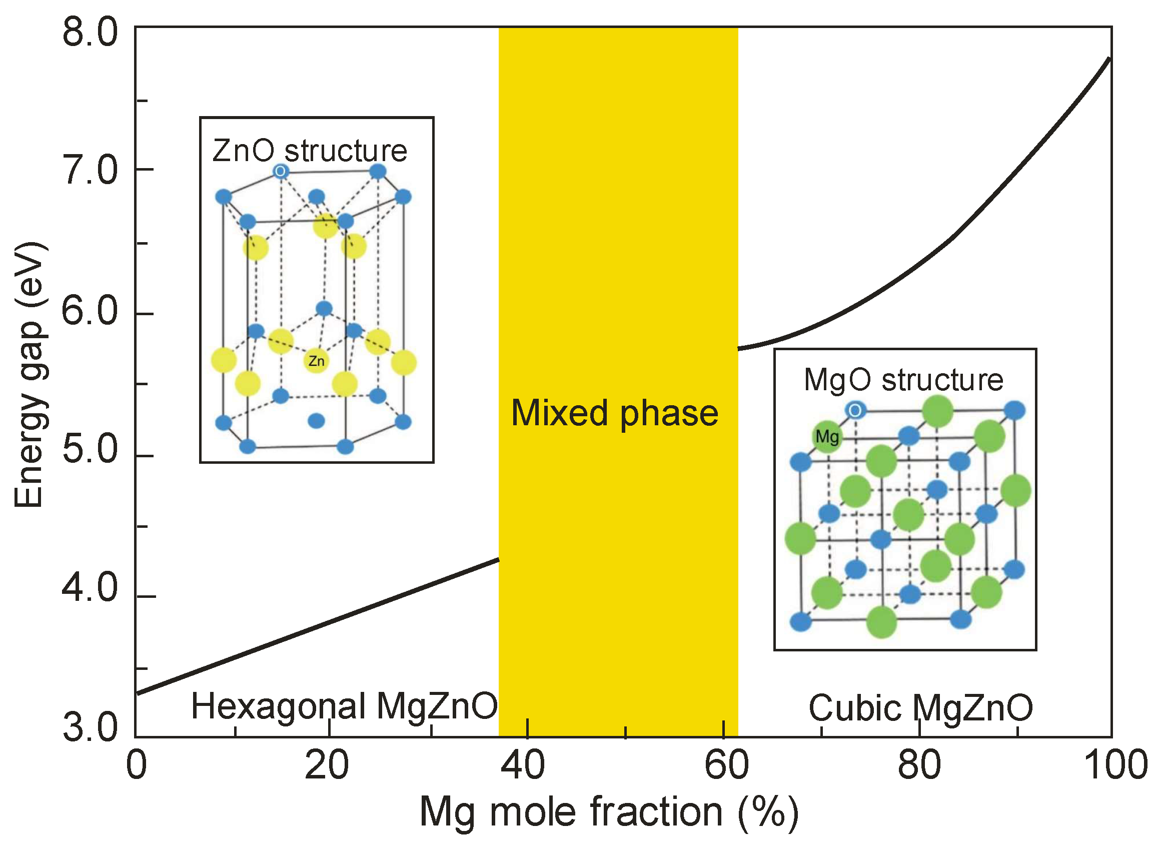
- Yang, W.; Hullavarad, S.S.; Nagaraj, B.; Takeuchi, I.; Sharma, R.P.; Venkatesan, T.; Vispute, R.D.; Shen, H. Compositionally-tuned epitaxial cubic MgxZn1−xO on Si(100) for deep ultraviolet photodetectors. Appl. Phys. Lett. 2003, 82, 3424–3426. [Google Scholar] [CrossRef]
- Hou, Y.; Mei, Z.; Du, X. Semiconductor ultraviolet photodetectors based on ZnO and MgxZn1−xO. J. Phys. D Appl. Phys. 2014, 47, 283001. [Google Scholar] [CrossRef]
- Yang, J.-L.; Liu, K.-W.; Shen, D.-Z. Recent progress of ZnMgO ultraviolet photodetector. Chin. Phys. B 2017, 26, 047308. [Google Scholar] [CrossRef]
- Yang, P.; Yan, R.; Fardy, M. Semiconductor Nanowire: What’s Next? Nano Lett. 2010, 10, 1529–1536. [Google Scholar] [CrossRef] [PubMed]
- Wu, Y.; Sun, X.-J.; Jia, Y.-P.; Li, D.-B. Review of improved spectral response of ultraviolet photodetectors by surface plasmon. Chin. Phys. B 2018, 27, 126101. [Google Scholar] [CrossRef]
- Chen, H.; Liu, K.; Hu, L.; Al-Ghamdi, A.A.; Fang, X. New concept ultraviolet photodetectors. Mater. Today 2015, 18, 493–502. [Google Scholar] [CrossRef]
- Kumar, A.; Khan, M.A.; Kumar, M. Recent advances in UV photodetectors based on 2D materials: A review. J. Phys. D Appl. Phys. 2022, 55, 133002. [Google Scholar] [CrossRef]
- Ouyang, W.; Chen, J.; Shi, Z.; Fang, X. Self-powered UV photodetectors based on ZnO nanomaterials. Appl. Phys. Rev. 2021, 8, 031315. [Google Scholar] [CrossRef]
- Lin, H.; Jiang, A.; Xing, S.; Li, L.; Cheng, W.; Li, J.; Miao, W.; Zhou, X.; Tian, L. Advances in Self-Powered Ultraviolet Photodetectors Based on P-N Heterojunction Low-Dimensional Nanostructures. Nanomaterials 2022, 12, 910. [Google Scholar] [CrossRef] [PubMed]
- Nguyen, T.M.H.; Shin, S.G.; Choi, H.W.; Bark, C.W. Recent advances in self-powered and flexible UVC photodetectors. Exploration 2022, 2, 20210078. [Google Scholar] [CrossRef]
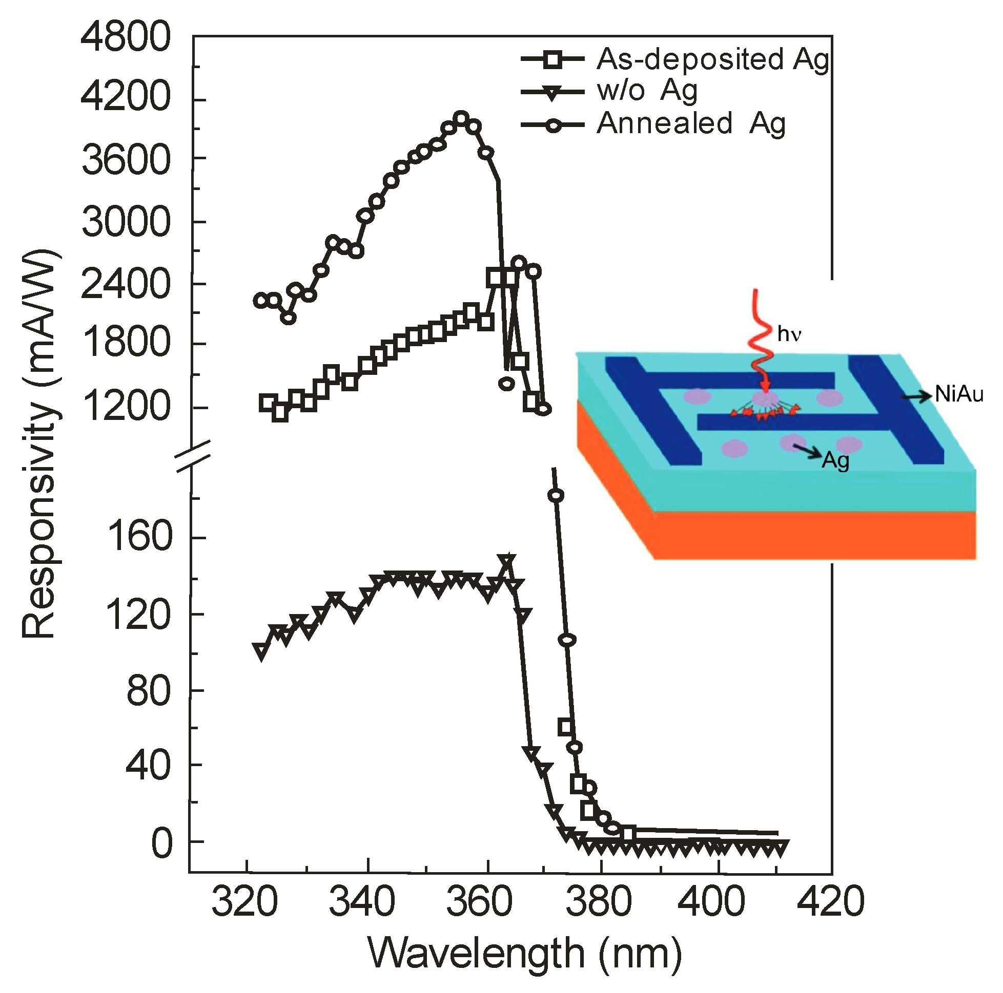
- Wang, X.; Liu, K.; Chen, X.; Li, B.; Jiang, M.; Zhang, Z.; Zhao, H.; Shen, D. Highly Wavelength-Selective Enhancement of Responsivity in Ag Nanoparticle-Modified ZnO UV Photodetector. ACS Appl. Mater. Interfaces 2017, 9, 5574–5579. [Google Scholar] [CrossRef]
- Zhang, W.; Xu, J.; Ye, W.; Li, Y.; Qi, Z.; Dai, J.; Wu, Z.; Chen, C.; Yin, J.; Li, J.; et al. High-performance AlGaN metal–semiconductor–metal solar-blind ultraviolet photodetectors by localized surface plasmon enhancement. Appl. Phys. Lett. 2015, 106, 021112. [Google Scholar] [CrossRef]
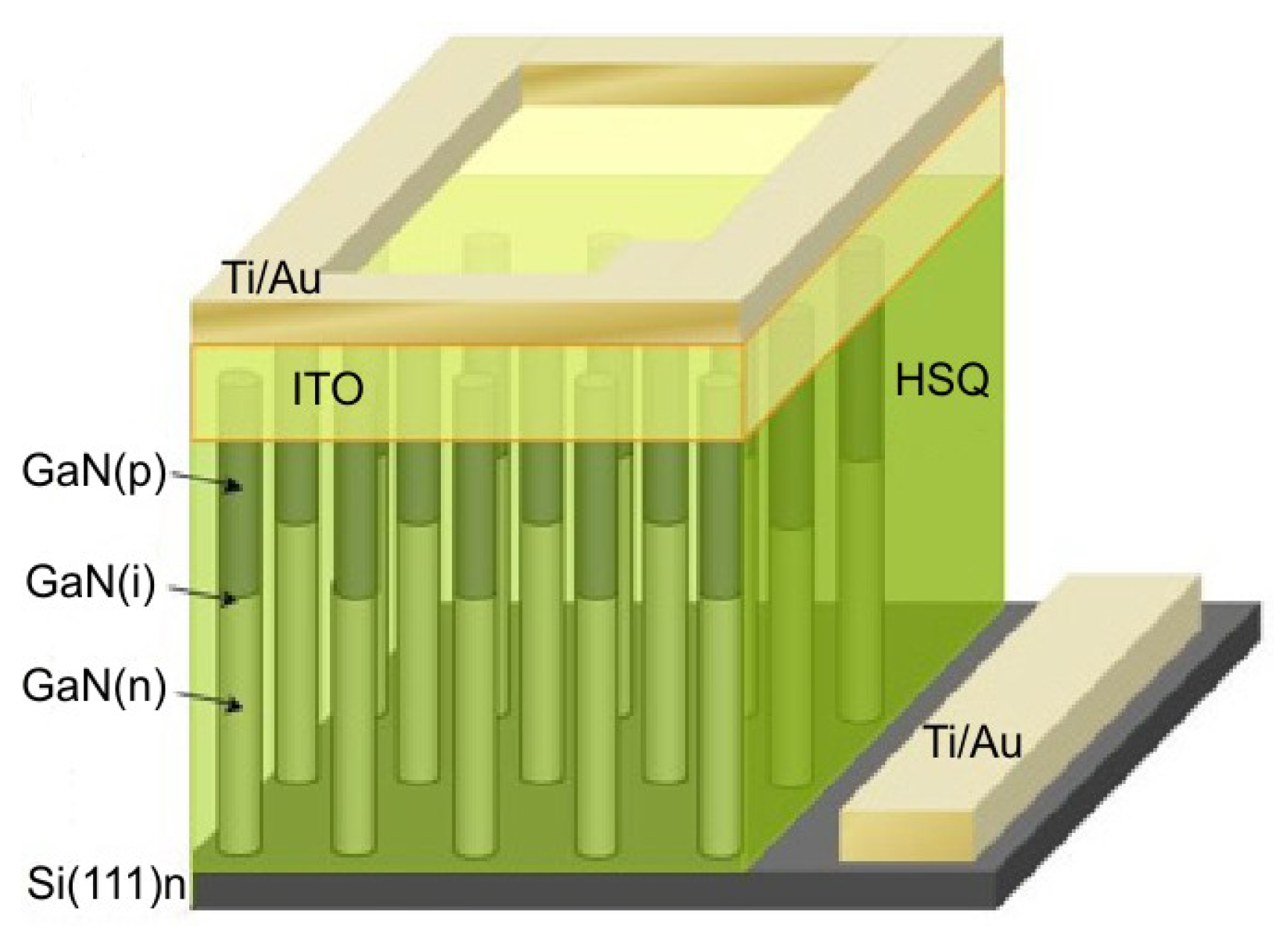
- de Luna Bugallo, A.; Tchernycheva, M.; Jacopin, G.; Rigutti, L.; Julien, F.H.; Chou, S.-T.; Lin, Y.-T.; Tseng, P.-H.; Tu, L.-W. Visible-blind photodetector based on p–i–n junction GaN nanowire ensembles. Nanotechnology 2010, 21, 315201. [Google Scholar] [CrossRef]
- Sang, L.; Hu, J.; Zou, R.; Koide, Y.; Liao, M. Arbitrary Multicolor Photodetection by Hetero-integrated Semiconductor Nanostructures. Sci. Rep. 2013, 3, 2368. [Google Scholar] [CrossRef]
- Wang, Y.; Wang, F.; Li, S.; Yang, J.; Yan, T.; Cai, Y.; Wu, Z.; Zhan, X.; He, J.; Wang, Z. Vertical Barrier Heterostructures for Reliable, Robust, and High-Performance Ultraviolet Detection. Small 2022, 18, 2204021. [Google Scholar] [CrossRef]
- Yuan, D.; Wan, L.; Zhang, H.; Jiang, J.; Liu, B.; Li, Y.; Su, Z.; Zhai, J. An Internal-Electrostatic-Field-Boosted Self-Powered Ultraviolet Photodetector. Nanomaterials 2022, 12, 3200. [Google Scholar] [CrossRef]
- Deka Boruah, B. Zinc oxide ultraviolet photodetectors: Rapid progress from conventional to self-powered photodetectors. Nanoscale Adv. 2019, 1, 2059–2085. [Google Scholar] [CrossRef] [PubMed]
- Xu, J.; Yang, W.; Chen, H.; Zheng, L.; Hu, M.; Li, Y.; Fang, X. Efficiency enhancement of TiO2 self-powered UV photodetectors using a transparent Ag nanowire electrode. J. Mater. Chem. C 2018, 6, 3334–3340. [Google Scholar] [CrossRef]
- Shen, L.; Fang, Y.; Wang, D.; Bai, Y.; Deng, Y.; Wang, M.; Lu, Y.; Huang, J. A Self-Powered, Sub-nanosecond-Response Solution-Processed Hybrid Perovskite Photodetector for Time-Resolved Photoluminescence-Lifetime Detection. Adv. Mater. 2016, 28, 10794–10800. [Google Scholar] [CrossRef] [PubMed]
- Shen, H.; Shan, C.X.; Li, B.H.; Xuan, B.; Shen, D.Z. Reliable self-powered highly spectrum-selective ZnO ultraviolet photodetectors. Appl. Phys. Lett. 2013, 103, 232112. [Google Scholar] [CrossRef]
- Ni, P.-N.; Shan, C.-X.; Wang, S.-P.; Liu, X.-Y.; Shen, D.-Z. Self-powered spectrum-selective photodetectors fabricated from n-ZnO/p-NiO core–shell nanowire arrays. J. Mater. Chem. C 2013, 1, 4445. [Google Scholar] [CrossRef]
- Li, L.; Hu, C.; Shen, G. Low-Dimensional Nanostructure Based Flexible Photodetectors: Device Configuration, Functional Design, Integration, and Applications. Acc. Mater. Res. 2021, 2, 954–965. [Google Scholar] [CrossRef]
- Li, Y.; Ma, H.; Hu, W.; Zhao, Y. Highly transparent oxide-based ultraviolet photodetectors for flexible electronics. J. Mater. Sci. Mater. Electron. 2022, 33, 15546–15553. [Google Scholar] [CrossRef]
- Chen, T.-P.; Young, S.-J.; Chang, S.-J.; Hsiao, C.-H.; Hsu, Y.-J. Bending effects of ZnO nanorod metal–semiconductor–metal photodetectors on flexible polyimide substrate. Nanoscale Res. Lett. 2012, 7, 214. [Google Scholar] [CrossRef] [PubMed]
- Young, S.-J.; Liu, Y.-H.; Shiblee, M.D.N.I.; Ahmed, K.; Lai, L.-T.; Nagahara, L.; Thundat, T.; Yoshida, T.; Arya, S.; Furukawa, H.; et al. Flexible Ultraviolet Photodetectors Based on One-Dimensional Gallium-Doped Zinc Oxide Nanostructures. ACS Appl. Electron. Mater. 2020, 2, 3522–3529. [Google Scholar] [CrossRef]
- Zhang, X.; Zheng, E.; Esopi, M.R.; Cai, C.; Yu, Q. Flexible Narrowband Ultraviolet Photodetectors with Photomultiplication Based on Wide Band Gap Conjugated Polymer and Inorganic Nanoparticles. ACS Appl. Mater. Interfaces 2018, 10, 24064–24074. [Google Scholar] [CrossRef] [PubMed]


| Type of Detector | Detector Structure | Diagram of Energy Band |
|---|---|---|
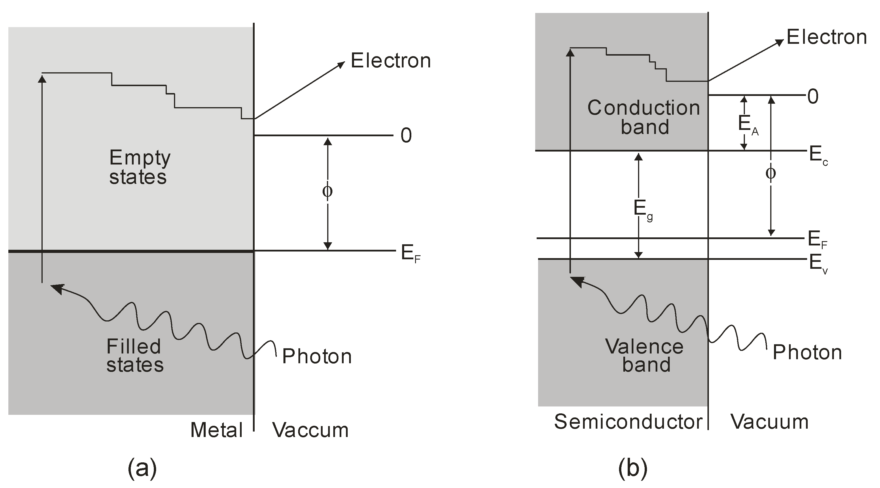
| Photoemissive detector The photoelectric effect involves the emission of electrons when optical radiation hits a photocathode with sufficiently high kinetic anergy, greater than the vacuum level barrier, to leave the photocathode and be emitted as a free electron. Suppose a large electric field is placed between the cathode and the anode. In that case, the emitted electrons are accelerated in the space between the detector electrodes, and the collecting anode produces a photocurrent proportional to the intensity of the incoming photon. In the photomultiplier tube (PMT), photoemitted electrons impact other dynodes specially placed in the tube, creating a cascade of emitted electrons by a secondary emission process. |  |  |
| Photoconductor It is an optical radiation-sensitive photoresistor in which incident radiation creates electron-hole pairs in a homogeneous semiconductor material directly across the band gap. This band gap determines the spectral response. During the same phenomenon, a quantum-well photoconductor photoexcites electrons or holes from the potential well in the band-gap regions of the semiconductor. |  |  |
| P–N junction photodiode This is a widely used photodetector in a typical p-on-n configuration with a shallowly diffused p-region on the n-type active layer. An n-on-p structure is also available. An electric field separates photo-created electron-hole pairs on either side of the junction in the space charge region. The generated photocurrent changes the open-circuit junction voltage or the short-circuit junction current. |  |  |
| P-i-N photodiode P-i-N is merely a standard photodiode in which an intrinsic i-region is incorporated between the P and N sides of the junction (a capital letter stands for a wider energy gap). The depletion region occupies the entire intrinsic volume of the reverse bias voltage. Only in this region do incident photons generate electron-hole pairs. If there is no electrically neutral volume, zero diffusion current in the device is observed, and minority carriers generated through defect centers in the diode depletion region compose the dark current. |  |  |
| Avalanche photodiode (APD) The avalanche photodiode detects extremely low-intensity radiation. The n+-n−-p architecture, with controlled doping profiles and a geometry that ensures a uniform electric field, is easy to produce. The high reverse bias generates the depletion layer across the n−region, and photons are absorbed in the p-region. The applied electric field accelerates photogenerated minority carrier electrons at the edge of the depletion region. Their collisions with the crystal lattice cause an avalanche of ionization. This process provides new carriers and causes a rapid increase in current flowing in the reverse direction. The APD offers a combination of high speed, high sensitivity, and high quantum efficiency. |  |  |
| Schottky barrier photodiode It is a majority carrier device formed at the metal-semiconductor junction. As with the p–n junction, this junction provides a potential barrier to separate photoexcited electron-hole pairs within the semiconductor or at the metal-semiconductor interface. Compared to a p-n photodiode, a Schottky barrier photodiode has some advantages, e.g., fabrication simplicity (deposition of the metal barrier on the n(p)-semiconductor), lower-temperature diffusion processes, and a higher reaction rate. However, a Schottky junction is generally characterized by a more significant dark current. |  |  |
| Metal-semiconductor-metal (MSM) photodiode This structure is similar to the interdigitated photoconductor, in which Schottky barriers fabricate the metal-semiconductor and semiconductor-metal junctions instead of ohmic contacts. Processing steps nearly identical to those required for making field-effect transistors are used to produce a planar structure with monolithic integration of the MSM photodiode. A lower dark current characterizes this type of design compared to a single Schottky diode and has a faster response speed than a p-i-n photodiode. |  |  |
| Metal-insulator-semiconductor (MIS) photodiode This device is built with an insulator separating the metal gate from the semiconductor surface. The thickness of the insulator must not fall below a minimum of about 10 nm. The use of thinner insulation than this leads to the occurrence of tunneling through the insulating layer. A negative voltage relative to the metal electrode creates a depletion region, repelling electrons from the insulator-semiconductor interface. Its “well capacitance” defines the total charge accumulated on a photogate. This capacitance depends on the gate bias, insulator thickness, electrode surface area, and semiconductor background doping. |  |  |
| Photo-FET The device’s configuration is similar to lateral photoconductors, with the MSM architecture forming the source and drain electrodes. The modulation of the channel conductivity is performed using a third gate electrode that is electrically isolated from the semiconductor channel by a thin dielectric layer. The VG gate voltage electronically controls the density of the carrier by modulating the field effect and advantageously switches off the dark current by operating the device in the depletion regime. The incident light activates the conductivity of the device channel by photo-generating the carriers, which then ideally benefit from the photoconductivity enhancement mechanism (photoelectric gain), as in photoconductors. |  |  |
| Parameters | Si | Diamond | 4H-SiC | 6H-SiC | GaN | AlN | ZnO | MgO | ZnSe | β-Ga2O3 |
|---|---|---|---|---|---|---|---|---|---|---|
| Energy gap (eV) | 1.12 | 5.45 | 3.26 | 3.02 | 3.4 | 6.2 | 3.37 | 7.83 | 2.58 | 4.85 |
| Density (g/cm3) | 2.329 | 3.52 | 3.21 | 3.21 | 6.15 | 3.32 | 5.61 | 3.58 | 5.42 | 5.95 |
| Thermal conductivity (W/cmK) | 1.45 | 22.9 | 3.7 | 4.9 | 3.2 | 4.6 | 5.4 | 4.82 | 0.18 | 0.20 |
| Melting point (K) | 1683 | 3773 | 3100 | 3100 | >2000 | >2500 | 2242 | 3073 | 1517 | 1795 |
| Electron saturation velocity (105 m/s) | 1 | 2.3 | 2.1 | 2 | 1.4 | 1.3 | 1.1 | |||
| Electron mobility (cm2/Vs) | 1240 | 7300 | 950 | 400 | 1000 | 420 | 170 | 10 | 540 | 300 |
| Hole mobility (cm2/Vs) | 480 | 5300 | 120 | 75 | 11 | 14 | 40 | 2 | 30 | 20 |
| Dielectric constant | 11.9 | 5.7 | 9.7 | 9.7 | 10.4 | 10.1 | 9.1 | 9.8 | 8.6 | 10 |
| Breakdown field (105 V/cm) | 3 | 130 | 31 | 24 | 49.5 | 154 | 103 |
| Structure | Dark Current/(Density) | Iph/Idark | Responsivity [A/W] | UV/VIS Rejection Ratio | trise/tfall | Ref. |
|---|---|---|---|---|---|---|
| GaN PIN | 8 × 10⁻¹⁰ A/cm2 | 8.4 × 10⁵ | 0.35 | 1.2 × 10⁴ | 75 µs/110 µs | [43] |
| GaN MSM | 1 pA | 1 × 10⁵ | 3.096 | 5 × 10⁴ | - | [44] |
| AlGaN MSM | 20 pA | 2.6 × 10⁵ | - | - | 25 ps | [45] |
| p-GaN/AlGaN/GaN on Si (λc = 395 nm) | 29 × 10−9 mA/mm2 | 1.7 × 10⁸ | 2 × 10⁴ | 1.1 × 10⁷ | 12.2 ms/8.9 ms | [46] |
| GaN PIN PC mode | 40 pA/cm2 (<2 fA) | - | 0.14 | 8 × 10³ | - | [47] |
| AlGaN/GaN PD (λc = 365 nm) | 50 nA | 1 × 10⁵ | 7 × 10⁴ | 104 | 6 ms * | [48] |
| AlGaN Schottky (λc = 310 nm) | 20 pA@1 V | 105 | 0.07 | - | 10 ns/190 ns | [49] |
| Structure | Substrate | Front/Back Illuminated | Electron/Hole Initiated | Breakdown Voltage(V) | Idark (A/cm2 at 95% BV) | Maximum Responsivity (A/W) | Maximum Gain | Ref. |
|---|---|---|---|---|---|---|---|---|
| GaN | GaN | Front | Hole | 278 | 1.5 × 10⁻⁵ | 60 | 105 | [62] |
| GaN | Sapphire | Back | Hole | 90 | 0.044 | 0.163 | 1.9 × 10⁴ | [64] |
| AlGaN (λc = 340 nm) | Sapphire | Back | Hole | 66.5 | 0.01 | 0.15 | 2 × 10⁴ | [65] |
| AlGaN (λp = 255 nm) | Sapphire | Back | Hole | 90 | 3.5 × 10⁻³ | 2 | 3 × 10³ | [66] |
| AlGaN (λp = 255 nm) | Sapphire | Back | Hole | 80 | 0.8 | NA | 5 × 10⁴ | [67] |
| Al0.05Ga0.95N | GaN | Front | Electron | 100 | 1 × 10⁻⁴ | 0.8 | 8 × 10⁵ | [68] |
| GaN | GaN | Front | Electron | 92.3 | 2 × 10⁻⁴ | 0.15 | 1.4 × 10⁴ | [69] |
| GaN | GaN | Front | Electron | 95.4 | 1 × 10⁻² | 0.14 | 2 × 10⁶ | [70] |
| Al0.05Ga0.95N | Sapphire | Front | Electron | 90 | 4.4 × 10⁻⁵ | NA | 2 × 10⁴ | [68] |
| GaN | Sapphire | Front | Electron | >120 | 1.27 × 10⁻⁴ | 0.23 | NA | [71] |
| GaN | Sapphire | Front | Electron | 92 | 795 | NA | 300 | [72] |
| GaN | SiC | Front | Electron | 160 | 2 × 10⁻⁸ | 4.2 | 105 | [73] |
| Material of Active Region | Pixel Structure | Array Format | Pixel Size (µm2) | Wavelength Range (nm) | Year | Ref. |
|---|---|---|---|---|---|---|
| AlGaN | p-i-n | 256 × 256 | 30 × 30 | 265–285 | 2001 | [80] |
| GaN | p-i-n | 320 × 256 | 24 × 24 | 300–365 | 2002 | [81] |
| Al0.32Ga0.68N | p-i-n | 320 × 256 | 25 × 25 | 280 | 2005 | [82] |
| AlGaN | p-i-n | 256 × 256 | - | 285–365 | 2005 | [83] |
| Al0.45Ga0.55N | p-i-n | 256 × 256 | 30 × 30 | 260–280 | 2006 | [84] |
| Al0.45Ga0.55N | Schottky | 320 × 256 | 30 × 30 | 280 | 2007 | [85] |
| Al0.59Ga0.41N | p-i-n | 128 × 128 | 50 × 50 | 233–258 | 2008 | [86] |
| Al0.43Ga0.57N | Schottky | 320 × 256 | 30 × 30 | 260–290 | 2009 | [87] |
| Al0.4Ga0.6N with Si-layer | Schottky | 256 × 256 | 10 × 10 | 1–33 | 2011 | [88] |
| Al0.45Ga0.55N | p-i-n | 320 × 256 | 25 × 25 | 290 | 2013 | [89] |
| Al0.4Ga0.6N | p-i-n | 320 × 256 | 25 × 25 | 278 | 2015 | [90] |
| Al0.43Ga0.57N | p-i-n | 640 × 512 | 15 × 15 | 280 | 2020 | [91] |
| Device | Active Region | Responsivity Peak (A/W) | Reverse Voltage (V) | Wavelength at Peak (nm) | Quantum Efficiency (%) | Dark Current/ (Density) | Ref. |
|---|---|---|---|---|---|---|---|
| Schottky | 6H-SiC | 0.070 | 0 | 320 | 28 | 0.2 nA/cm2 | [106] |
| Schottky | 4H-SiC | 0.093 | −15 | 270 | 87.9 | <70 fA | [107] |
| Schottky | 4H-SiC | 0.073 | −10 | 290 | 31.2 | <1 pA @, 0 V | [108] |
| Schottky | 4H-SiC | 0.115 | 0 | 285 | 50 | 1 pA (20 V, 100 °C) | [109] |
| p-i-n | 4H-SiC | 0.15 | −5 | 268 | - | 1.8 pA @ RT | [105] |
| p-i-n | 4H-SiC | 0.13 | −5 | 270 | 61 | 2.5 pA/mm2 | [110] |
| p-i-n | 4H-SiC | 0.204 | −30 | 285 | 88.3 | 38.6 nA/cm2@-10 V | [111] |
| λpeak (nm) | Responsivity Peak (A/W) | V (V) | Gain (M) | k | QE (%) | Dark Current */(Density) | Ref. |
|---|---|---|---|---|---|---|---|
| 280 | 0.093 | 144 | 1.4 × 10⁴ | 0.1 | 41 | 63 nA/cm2 at M = 1 | [113] |
| 290 | 0.080 | 112 (M = 100) | 103 | 0.1 | 35 | 9.2 µA/cm2 at M | [112] |
| 274 | 0.18 | ~156 | 106 | - | 81.5 | 0.2 nA/cm2 | [117] |
| 270 | 0.203 | 42 | 1.8 × 10⁴ @55 V | - | 93 | <10 pA@27.5 V | [115] |
| 270 | 0.100 | 30 | 105@94 V | - | 45 | 10 nA@30 V | [116] |
| Material /Device * | Responsivity (A/W)@220 nm | Dark Current (A) | Response Time | Rejection Ratio | Ref. |
|---|---|---|---|---|---|
| PC/BSCD PC/SCD PC/Polylicryst. | 6 at 3 V 21.8 at 50 V 0.63 at 222 nm | 10−12 @20 V - 0.3 × 10⁻⁹ | <10 ns Rise 310 µs/Decay 330 µs - | 108 8.9 × 10³ 106 | [127] [129] [137] |
| MSM MSM | 230 at 1 V 0.02 at 6 V | 10−12@0.4 V Few pA | - - | 106 104 | [133] [138] |
| Schottky BSCD Polycrystalline | 18 at −23 V 10 at 100 V | 10−14@−23 V - | 1–10 ms Rise 5 ms/Decay 8 ms | 108 104–105 | [135] [139] |
| PD/pin | 27 mA/W@200 nm | 4 × 10⁻¹³ | - | 106 | [136] |
| Parameter | Ga2O3 | Si | 4H-SiC | GaN | AlN | Diamond |
|---|---|---|---|---|---|---|
| Energy gap (eV) | 4.5–5.3 | 1.1 | 3.3 | 3.4 | 6.2 | 5.5 |
| Breakdown field (MV/cm) | 5–9 | 0.3 | 2.6 | 3.3 | 2 | 10 |
| Electronic mobility (cm2/Vs) | 300 | 1400 | 1000 | 1200 | 155 | 2000 |
| Thermal conductivity (W/cmK) | 0.23 (010) 0.13 (100) | 1.5 | 2.7 | 2.1 | 13 | 22 |
| Baliga’s FOM ( | 3443 | 1 | 340 | 870 | - | 24,664 |
| Johnson’s FOM | 1093 | 1 | 177.6 | 756 | - | - |
| Substrate size (inch) | 6 | 12 | 8 | 2 | 2 | 1 |
| Response spectrum (nm) | <280 | 400–1100 | 200–370 | 200–300 | <200 | <225 |
| Structure | λ [µm] | R (A/W) | EOE (%) | Dark Current (A) | Rejection Ratio | D* (Jones) | Response Time (tr/td) |
|---|---|---|---|---|---|---|---|
| β-Ga2O3/spiro-MeOTAD | 254 | 6.5 × 10⁻² (0 V) | 32 | 7.5 × 10⁻¹⁴ | 3.6 × 10³ | 3.95 × 10¹¹ | 0.21 s/0.07 s |
| β-Ga2O3/MoS2 | 245 | 2.05 × 10⁻³ (0 V) | - | 0.9 × 10⁻¹² | 1.6 × 10³ | 1.21 × 10¹¹ | - |
| Ga2O3/graphene | 200 | 12.8 (−6 V) | - | 1.2 × 10⁻⁸ | - | 1.3 × 10¹³ | 0.0015 s/0.002 s |
| Ga2O3/polyaniline | 246 | 2.1 × 10⁻² (0 V) | - | 0.8 × 10⁻¹³ | 102 | 1.5 × 10¹¹ | 0.00034 s/0.00814 s |
| amorphous-Ga2O3 | 250 | 607.11 | 3.0 × 10⁵ | - | - | 5.15 × 10¹⁴ | 0.65 s/1.18 s |
| Ga2O3 nanobelts | 250 | 851 | 4.2 × 10³ | 1.0 × 10⁻¹³ | - | - | <0.3 s/<0.3 s |
| ZnO-Ga2O3 core shell | 254 | 1.3 × 10³ (−6 V) | 2.5 × 10⁶ | 5.35 × 10⁻¹⁰ | 5 × 10³ | 9.91 × 10¹⁴ | 2 × 10⁻⁵ s/4.2 × 10−5 s |
| Au/β-Ga2O3/ZnO | 254 | 1.1 × 10⁴ (−40 V) | - | >1.0 × 10⁻¹² | 103 | 9.6 × 10¹² | <0.000563 s/0.000238 s |
| β-Ga2O3 | 254 | 4.24 × 10⁴ | 2 × 10⁵ | - | - | 1.7 × 10¹¹ | - |
| β-Ga2O3 micro flakes | 254 | 1.7 × 10⁵ | 8.3 × 10⁷ | 27 × 10−15 | 2.4 × 10⁴ | 1.1 × 10¹⁸ | 0.428 s/0.435 s |
| β-Ga2O3 phototransistor | 254 | 1.4 × 10⁷ | 6.4 × 10⁷ | - | 6.0 × 10⁷ | 1.1 × 10¹⁹ | -/0.016 s |
| β-Ga2O3/MgO flakes | 260 | 2.4 × 10⁷ | - | 6.7 × 10⁻¹² | - | 1.7 × 10¹⁵ | 6.38 s/0.07 s |
| Material/Structure | λc (nm) | Ri (A/W) | Dark Current (pA) | Rejection Ratio | Response Time (µs); tr/td |
|---|---|---|---|---|---|
| w-ZnMgO/MSM | 310 | 34.02 | 7.67 × 10³ (5 V) | 2660 | 44/1.2 × 105 |
| w-ZnMgO/MSM | 350 | 2.1 (10 V) | 0.73 (5 V) | 5.46 × 10⁵ | 2 × 10⁸/6 × 107 |
| w-Zn0.6Mg0.4O/p-Si heterojunction | 300 | 0.22 (−2 V) | 700 (−3 V) | 102 | 1 × 10⁶ |
| w-Zn0.5Mg0.5O/p-Si heterojunction | 208 301 | 0.013 (1 V) 0.006 (−2 V) | 2 × 10³ | 102 | 105/105 |
| m-Zn0.38Mg0.62O/MSM | 275 | 1.66 (10 V) | 8.29 (40 V) | 103 | 15/- |
| m-Zn0.59Mg0.41O/MSM | 320 | 89.8 (40 V) | 11 (40 V) | 105 | -/3 × 104 |
| Materials | Wavelength (nm) | Responsivity (A/W) | Response Time (Rise/Delay) | Detectivity (Jones) |
|---|---|---|---|---|
| 2D materials | ||||
| Few-layer BP | 310–390 | 9 × 10⁴ | 1 ms/4 ms | 3 × 10¹³ |
| WS2 | 365 | 53.3 | - | 1.2 × 10¹¹ |
| GaS | 254 | 19.2 | - | 1 × 10¹⁴ |
| BiOBr | 340 | 15.0 | 80 ms/40 ms | 5.7 × 10¹⁰ |
| CuGaS2 nanosheets | 254 | 5.1 | 1.8 s/10.1 s | 1.7 × 10¹¹ |
| Graphene quantum dots | 254 | 2.1 × 10⁻³ | 64 ms/43 ms | 9.6 × 10¹¹ |
| 2D heterostructure and hybrid | ||||
| MoS2/Cs3Bi2I9 | 325 | 1.42 | 11.6 ms/14.9 ms | 1.2 × 10¹³ |
| Graphene/GaN | 300–360 | 0.23 | 2.5 ms/2.5 ms | |
| BP/MoS2 | 365 | 77.2 | - | 6.5 × 10⁹ |
| Graphene/poly-BrNpA | 365 | 149 | - | 1.6 × 10¹¹ |
| Self-powered | ||||
| p-GaSe/n-WS2 | 270–740 | 0.149 | 37 ms/43 ms | 4.3 × 10¹² |
| SnS2/ZnO1−xSx | 365 | 8.3 × 10⁻³ | 49.5 ms/25.9 ms | 5.1 × 10¹⁰ |
| Bi2Te3 nanoshets | 365 | 6.3 × 10⁻³ | 12 ms/32 ms | - |
| Graphene/Si | 365 | 0.12 | 5 ns | 4.3 × 10¹² |
| Flexible | ||||
| GaS | 254 | 19.2 | 30 ms | 1 × 10¹⁴ |
| MAPbI3 | 264 | 1.2 | 2.2 ms/4 ms | 1 × 10¹¹ |
| ITO/ZnO/PI | 360 | 0.0125 | 3.24 s/108.7 ms | 2.71 × 10¹¹ |
| ZnS/MoS2 | 365 | 9.5 × 10⁻⁶ | 22 ms | - |
| Ca2Nb3O10 | 280 | 14.9 | 0.08 ms/5.6 ms | 8.7 × 10¹³ |
| Type of Photodetector | Advantages | Disadvantages |
|---|---|---|
| Photoconductive detector | Simple design, easy process of technological control, high photoelectrical gain | Large dark current, slow response time, generally lower detectivity in comparison with p-n photodiode |
| p-n and p-i-n photodiodes | High impedance, low dark current, fast response time, high-frequency operation, low-bias or self-powered operation | Spectral characteristic depends on the doping level of the active region, higher doping level worsens the spectral sensitivity |
| Phototransistor | Very high responsivity, very large photogating effect | Complicated technology, slow response time |
| Schottky barrier | Simple fabrication process, good responsivity, short response time, | Absorption losses, saturation dark current considerably higher than in p–n junction (due to lower built-in voltage) |
| Metal-semiconductor-metal (MSM) | Simple fabrication process, fast response time, lower dark current compared to a single Schottky diode, easy integration | Lower spectral response and quantum efficiency |
Disclaimer/Publisher’s Note: The statements, opinions and data contained in all publications are solely those of the individual author(s) and contributor(s) and not of MDPI and/or the editor(s). MDPI and/or the editor(s) disclaim responsibility for any injury to people or property resulting from any ideas, methods, instructions or products referred to in the content. |
© 2023 by the authors. Licensee MDPI, Basel, Switzerland. This article is an open access article distributed under the terms and conditions of the Creative Commons Attribution (CC BY) license (https://creativecommons.org/licenses/by/4.0/).
Share and Cite
Rogalski, A.; Bielecki, Z.; Mikołajczyk, J.; Wojtas, J. Ultraviolet Photodetectors: From Photocathodes to Low-Dimensional Solids. Sensors 2023, 23, 4452. https://doi.org/10.3390/s23094452
Rogalski A, Bielecki Z, Mikołajczyk J, Wojtas J. Ultraviolet Photodetectors: From Photocathodes to Low-Dimensional Solids. Sensors. 2023; 23(9):4452. https://doi.org/10.3390/s23094452
Chicago/Turabian StyleRogalski, Antoni, Zbigniew Bielecki, Janusz Mikołajczyk, and Jacek Wojtas. 2023. "Ultraviolet Photodetectors: From Photocathodes to Low-Dimensional Solids" Sensors 23, no. 9: 4452. https://doi.org/10.3390/s23094452