Communication

Visible Near-Infrared Photodetection Based on Ta2NiSe5/WSe2 van der Waals Heterostructures

1
College of Science, Zhejiang University of Technology, 288 Liu-He Road, Hangzhou 310023, China
2
College of Physics and Optoelectronic Engineering, Hangzhou Institute for Advanced Study, University of Chinese Academy of Sciences, No. 1, Sub-Lane Xiangshan, Xihu District, Hangzhou 310024, China
3
State Key Laboratory for Infrared, Physics Shanghai Institute of Technical Physics, Chinese Academy of Sciences, 500 Yu-Tian Road, Shanghai 200083, China
*
Author to whom correspondence should be addressed.
Sensors 2023, 23(9), 4385; https://doi.org/10.3390/s23094385
Submission received: 20 March 2023 / Revised: 14 April 2023 / Accepted: 15 April 2023 / Published: 29 April 2023
(This article belongs to the Special Issue Recent Progress on Advanced Infrared/Terahertz Photodetectors)

Abstract

:
The increasing interest in two-dimensional materials with unique crystal structures and novel band characteristics has provided numerous new strategies and paradigms in the field of photodetection. However, as the demand for wide-spectrum detection increases, the size of integrated systems and the limitations of mission modules pose significant challenges to existing devices. In this paper, we present a van der Waals heterostructure photodetector based on Ta2NiSe5/WSe2, leveraging the inherent characteristics of heterostructures. Our results demonstrate that this detector exhibits excellent broad-spectrum detection ability from the visible to the infrared bands at room temperature, achieving an extremely high on/off ratio, without the need for an external bias voltage. Furthermore, compared to a pure material detector, it exhibits a fast response and low dark currents (~3.6 pA), with rise and fall times of 278 μs and 283 μs for the response rate, respectively. Our findings provide a promising method for wide-spectrum detection and enrich the diversity of room-temperature photoelectric detection.

1. Introduction

The photoelectric industry has been experiencing continuous development over the past few decades and photoelectric devices have become ubiquitous in our daily lives. As the core of photoelectric devices, the photo-detector is a type of application equipment that converts optical signals into electrical signals. It is a key component of equipment that is frequently used in various fields such as medical diagnosis, optical communication, security monitoring, and military applications [1,2,3,4,5]. Conventional photodetectors, including Si, SiC, GaN, and ZnO [6,7], exhibit excellent single-band optical responses due to their band gaps. Silicon-based materials are generally used in visible light detectors, which have a wide range of applications in color imaging for realistic everyday scenes, while wide-bandgap semiconductor materials such as SiC, GaN, and ZnO are more suitable for UV detectors and have a wide range of application scenarios for anti-missile and tracking in the solar blind range of ultraviolet light [8,9]. However, as the application of photodetectors expands, the need to identify complex working environmental information is increasing. In the face of wide-spectrum detection, multiple detectors of different bands are often required to perform together; however, there has been a gradual failure to meet the current needs of the actual photoelectric application field. Therefore, the research on and development of broadband photodetectors that can cover multi-band response is particularly urgent at present [10,11,12].
Over the past decade, two-dimensional (2D) materials have gradually attracted considerable attention due to their atomic thin thickness, bandgap tunability, and easy integration of van der Waals (vdWs) heterostructures [13,14,15,16,17]. In particular, graphene possesses a zero bandgap and high carrier mobility, making it an attractive material for broadband response research. However, its natural spectrum absorption is only 2.3% and its zero bandgap results in relatively low response performance and limitations in photodetection research [18]. While single-layer MoS2 has demonstrated superior performance in the visible spectrum range, its application in the infrared spectrum of equal width is significantly restricted by its large bandgap [19,20,21,22]. Although black phosphorus (BP) exhibits a tunable narrow-bandgap (0.3–1.5 eV) and high carrier mobility, its poor stability currently impedes its widespread utilization in photoelectric detection research [23,24,25,26]. Recently, terephthalic thiocompound (Ta2NiSe5), a layered material with weak van der Waals force interactions, has shown significant potential in wide-band photodetection [27,28]. Unlike other two-dimensional materials, Ta2NiSe5 is a ternary chalcogenide compound that possesses a direct narrow bandgap (Eg ~ 0.33 eV) [29,30,31,32]. However, the Ta2NiSe5 photodetector suffers from the drawbacks of excessive dark current and high power consumption, which restrict its wide application in the field of photodetection [33]. The fabrication of heterogeneous devices may offer a potential solution to these problems associated with Ta2NiSe5. Heterojunctions based on two-dimensional materials can achieve self-powered, high photo response and a good signal ratio, which is determined by the mechanism of photocurrent generation. Moreover, in some structures, the appearance of heterogeneous interface Schottky barriers generates a built-in electric field that separates the electron-hole pairs generated by light, thereby inhibiting the rapid recombination of photocarriers [34,35,36].
In this work, we fabricated a photodetector by constructing a Ta2NiSe5/WSe2 van der Waals heterostructure on a metal electrode. A series of experimental data showed that Ta2NiSe5/WSe2 heterojunctions not only reduce the dark current and power consumption of single-material photodetectors by utilizing the Schottky barrier formed but also address the issue of limited detection bands in single-material photodetectors, thereby enabling wide-spectral detection from visible to infrared light. They also show good application potential in the field of visible light imaging. Our experimental results confirm the feasibility of Ta2NiSe5/WSe2 heterojunction photodetectors for wide-spectrum detection, low power consumption, and fast response.

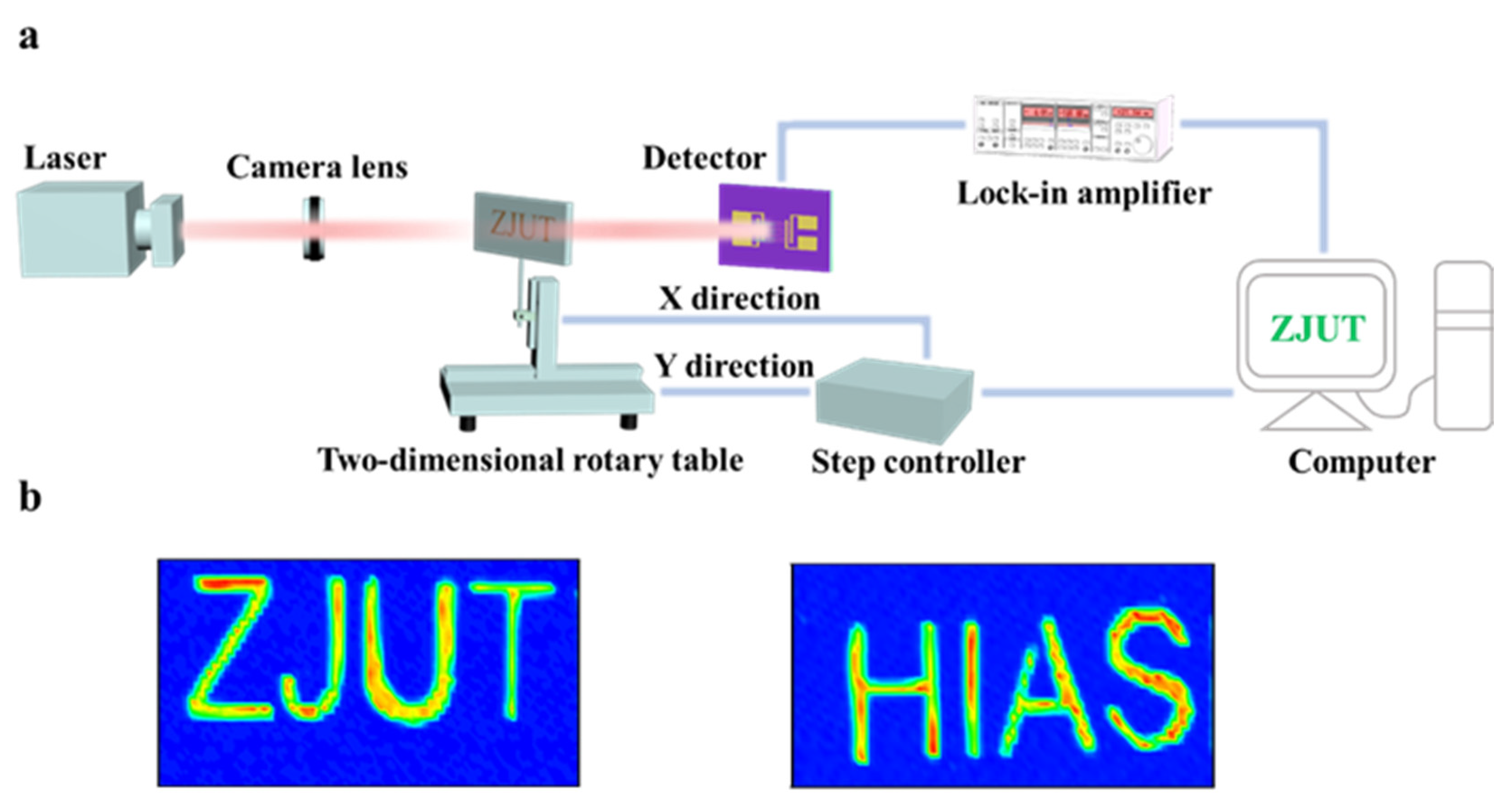
2. Device Design and Fabrication

We obtained bulk Ta2NiSe5 and WSe2 single crystals from Shanghai Onway Technology Co., Ltd. (Shanghai, China). Few-layer Ta2NiSe5 and WSe2 were exfoliated using scotch tape and then assembled using the all-dry transfer method to form van der Waals heterojunctions. As illustrated in Figure 1, the Ta2NiSe5/WSe2 heterostructure was constructed using the all-dry transfer method, which shows the process of heterojunction fabrication. Initially, we mechanically peeled off Ta2NiSe5 sheets of appropriate size using tape, followed by placing polydimethylsiloxane (PDMS) as an intermediate carrier onto the tape with the materials during the transfer process. Subsequently, we oriented the other side of the PDMS towards the substrate, with the material side facing down, to transfer the Ta2NiSe5 sheet onto the substrate. To transfer the WSe2 sheets, a similar technique was employed, but with the added requirement of operating and observing the specific position under a microscope in real-time to ensure the successful stacking of the WSe2 sheet onto the Ta2NiSe5 sheet to obtain a complete Ta2NiSe5/WSe2 heterojunction.
In this study, we investigated the photoelectric performance of the Ta2NiSe5/WSe2 heterojunction device under various environmental conditions in real-time, as illustrated in Figure 2a. Initially, Cr/Au (10 nm/50 nm) metal electrodes were deposited onto a low-resistance silicon substrate coated with SiO2 (300 nm) using UV lithography technology. Next, the Ta2NiSe5 sheet, prepared by mechanical exfoliation, was placed on the substrate via the standard PDMS pressing method, with the same preparation transfer process for the WSe2 sheet, to create a Ta2NiSe5/WSe2 heterostructure. The experimental materials were characterized using optical microscopy (Olympus BX51M), scanning electron microscopy with X-ray energy dispersive spectroscopy (SEM-EDS) (Zeiss/GEMINISEM 360), and microscopic laser confocal Raman spectroscopy (Dugout/LABRAM ODYSSEY). Figure 2b presents the optical image of the Ta2NiSe5/WSe2 heterostructure-based photodetector, with A–D denoting the four electrode directions. Different electrodes were connected to apply voltage for the performance testing of various devices. The scanning electron microscopy (SEM) image and corresponding energy dispersive spectra (EDS) mappings are shown in Figure 2c. The Raman spectra of the Ta2NiSe5, WSe2, and Ta2NiSe5/WSe2 heterojunction are represented in Figure 2d. For pure Ta2NiSe5 [37], three characteristic peaks located at 97.7, 121.8, and 288.8 cm−1, attributed to the Ag vibration mode, can be clearly observed and are denoted by the orange line. For pure WSe2 [38], the Raman spectrum exhibited two distinct diffraction peaks at 247.3 and 257.6 cm−1, corresponding to the E2g and A1g lattice vibrational modes in WSe2, respectively (red line). It has been reported that monolayers of WSe2 do not produce the characteristic peak at 308.3 cm−1 under 532 nm laser excitation [39], and the presence of this peak suggests that the exfoliated WSe2 flakes were less laminated. All the vibration modes of the Ta2NiSe5/WSe2 heterojunction, regardless of whether Ta2NiSe5 or WSe2 was used (blue line), were clearly observed in the overlapping region, indicating the effective preparation of the Ta2NiSe5/WSe2 heterojunction. According to previous reports, the conductance band (Ec) and valence band (Ev) of Ta2NiSe5 (WSe2) are located at −4.6 eV (−4.2 eV) and −5.28 eV (−4.93 eV) [40,41,42,43,44], respectively, forming the type I band alignment of the heterostructure. Figure 2e shows the band structure before and after contact. When the two materials came into contact to form the heterojunction, electrons flowed from Ta2NiSe5 to the latter due to a higher Fermi energy level than that for Ta2NiSe5, resulting in a depletion layer near Ta2NiSe5 and an accumulation layer on the other side, gradually forming an internal electric field [45,46]. The direction of the electric field went from Ta2NiSe5 to WSe2. Applying a forward bias reduced the barrier, facilitating the flow of electrons from Ta2NiSe5 to WSe2, resulting in an increase in current. Conversely, under reverse bias, the barrier increased, impeding the movement of electrons and causing a decrease in current, as illustrated in Figure 2f.

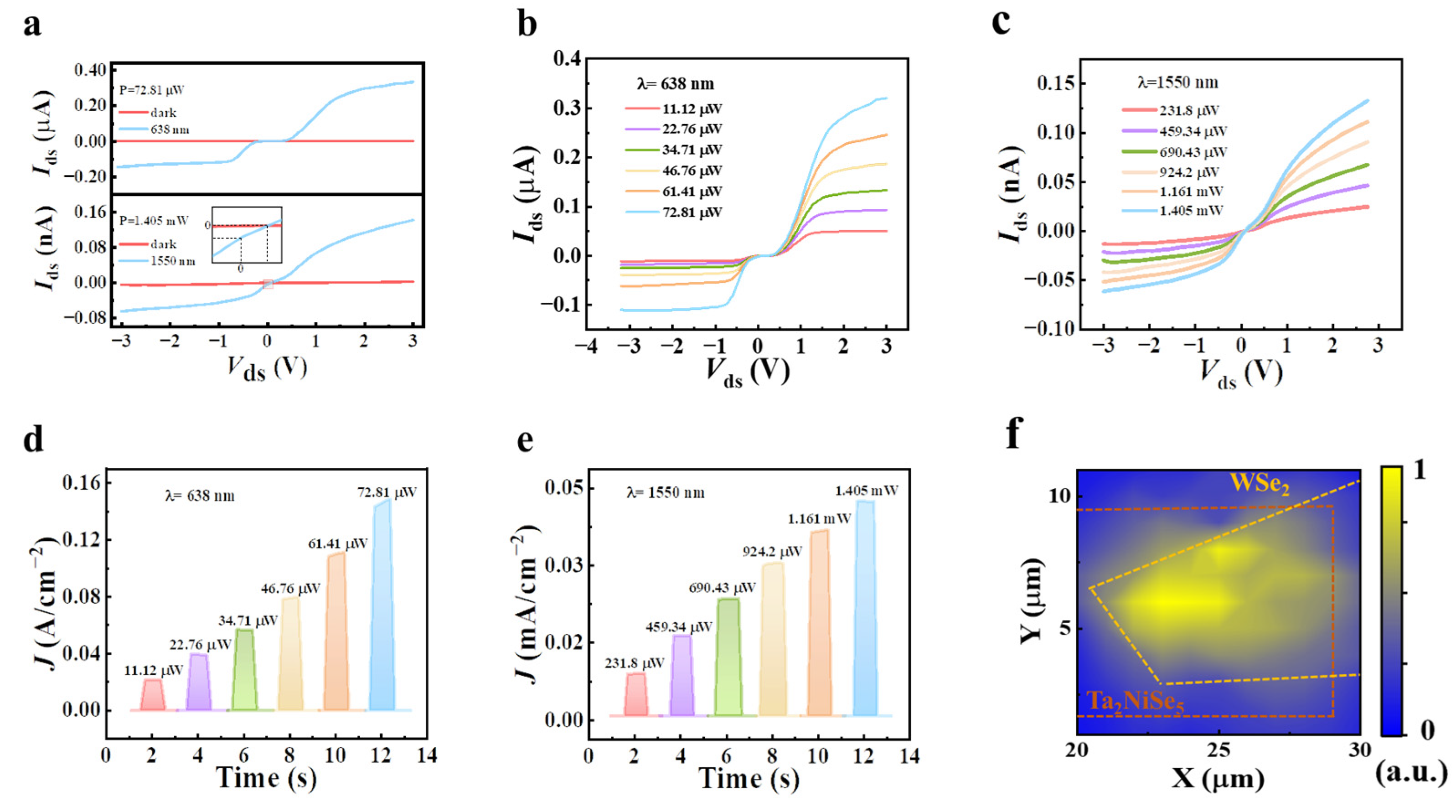
3. Results and Discussion

Before discussing the photoelectric performance of the Ta2NiSe5/WSe2 heterojunction detectors, certain photoelectric properties of the individual detector unit are examined to emphasize the advantages of heterojunction detectors. The external circuit was connected to electrodes B and D to conduct the photoelectric performance test of the few-layered WSe2 detector. Figure 3a displays the current–voltage (IV) curve of the few-layered WSe2 photodetector in the dark, which exhibited Schottky characteristics at room temperature and provided a built-in electric field in the device (Mstarter 200). The optoelectronic properties of the few-layered WSe2 photodetector were evaluated by varying the incident power (P) of 638 nm visible radiation, as shown in Figure 3b. Additionally, Figure 3c depicts the time-resolved photo responses of the various incident powers collected by high-speed oscilloscopes at room temperature without any bias voltage, where the photocurrent Iph and the current density J are obtained using Equations (1) and (2):
I ph = I ds I dark
J = I ds / S
where Ids represents the source-drain current under illumination, Idark represents the source-drain current in the dark, and S represents the effective area of the device. To elucidate the photocurrent generation mechanism of the few-layered WSe2 photodetector, scanning photocurrent microscopy mapping was performed without bias voltage under 638 nm laser irradiation at room temperature. As observed in Figure 3d, the area of the device was mainly distributed between the material and the metal electrode, and there was clear carrier movement within the device, displaying excellent photo response performance. The intrinsic Schottky junction facilitated the rapid separation and collection of electron-hole pairs, producing a photovoltaic current at visible radiation. However, due to the large bandgap limitation of WSe2, the detector failed to detect the photo response in the infrared band.
To unveil the photo response of the few-layered Ta2NiSe5 device in the infrared band, we characterized its optical image by switching on electrodes A and C, as shown in the inset of Figure 4a. In contrast to the WSe2 device, the current–voltage (IV) curve of the Ta2NiSe5 device exhibited excellent linearity in the dark, as depicted in Figure 4a. Here, the dark current was measured to be 126 uA at a bias voltage of −0.1 V. Figure 4b presents the linear current–voltage output curve of the Ta2NiSe5 device under illumination of 1550 nm. However, due to a large dark current, the photocurrent was not very apparent, even after applying the bias voltage. To further assess the photo response at 1550 nm, we measured the time-resolution photo response under periodic illumination with a fixed bias (Vds = 0.1 V) by switching to different optical powers (see Figure 4c, which shows a significant power dependency). In the near-infrared band, since the energy of the incident photon exceeded the bandgap of Ta2NiSe5 (hv > Eg), the photoinduced electron-hole pairs were separated by an external electric field and collected by the electrodes. The scanning photocurrent microscopy mapping revealed that the photocurrent region was far from the contact region of the electrode and Ta2NiSe5 material. It is noteworthy that, although the Ta2NiSe5 material is capable of realizing near-infrared photodetection, it is uncompetitive for future applications due to the large dark current caused by bias in photoconductivity mode.
The experimental results of the detectors based on the two individual materials mentioned above led to the proposal of a novel Ta2NiSe5/WSe2 vdWs heterogeneous structure that achieves low dark current levels from visible to infrared detection. During the testing process, we varied the wiring configuration by connecting the source and drain electrodes at terminals C and D. The current–voltage (IV) output curve of the vdWs heterogeneous device at room temperature with and without laser illuminations of 638 nm and 1550 nm, respectively, is presented in Figure 5a. By increasing the light incident power of 638 nm and 1550 nm, the Ta2NiSe5/WSe2 heterojunction device exhibited excellent photo response performance, as shown in Figure 5b,c, where a heterojunction is clearly visible. The phenomenon of negative short-circuit current (~4.3 pA) and positive open-circuit voltage (~0.1 V), as revealed in Figure 5a–c, is indicative of a photovoltaic-type mode. At a bias voltage of −1 V, the dark current of the proposed device was measured to be 3.6 pA, which is eight orders of magnitude lower than that of the Ta2NiSe5 device. The presence of the heterojunction not only reduced the dark current and improved the signal-to-noise ratio but also enhanced the light on/off ratio of the photocurrent. Figure 5d,e demonstrate the time-resolved photo response without any external electric field and with increasing incident power at 638 nm and 1550 nm, respectively, showing a fast photo-switching process. To further confirm the photo response mechanism, the location of the scanning photocurrent mapping focused on the junction area (see Figure 5f), which confirmed the origin of the photocurrent at the heterojunction. In the heterojunction region, electrons in Ta2NiSe5 were excited to the conduction band by IR radiation, generating electron-hole pairs, which were separated by the built-in electric field and flowed towards WSe2, being ultimately collected by electrodes. Conversely, holes flowed in the opposite direction, forming a circuit and producing photocurrent.
As illustrated in Figure 6a,b, photocurrent was observed in both the visible and infrared bands of the Ta2NiSe5/WSe2 heterojunction device, without applying any bias. Laser irradiation of the Ta2NiSe5/WSe2 heterojunction device generated photogenerated electrons, which then moved directionally to form photocurrent under the influence of the built-in electric field within the device. To evaluate the crucial parameters of the Ta2NiSe5/WSe2 heterojunction photodetector, responsivity R, characterized as the value of the photocurrent generated per unit of optical power, is defined as follows [47]:
R = I ph / P in
Specific detectivity D* is another important parameter of the photodetector and represents the sensitivity of the photodetector; it is defined as follows [48]:
D * = R / 2 q I d a r k / S 0.5
where Iph is the photocurrent, Pin is incident light power, q is the elementary charge, and S is the illumination active area on the device. For the visible/IR band, the extracted power-dependent responsivity and detectivity are plotted in Figure 6c,d. The responsivity of the heterojunction device was ~0.04 mA/W (P = 11.12 μW) at 638 nm and ~0.82 nA/W (P = 231.8 μW) at 1550 nm. The detectivity of the heterojunction device was approximately 3.6 × 10⁵ Jones (P = 11.12 μW) at 638 nm and approximately 90 Jones (P = 231.8 μW) at 1550 nm. Figure 6e presents the time-resolved optical response at 638 nm in the absence of any external electric field, revealing a rapid optical switching process. During this period, the photocurrent response of the device remained relatively stable, indicating good stability of the heterojunction device.
Response time, another key parameter, which is routinely defined as the time required by the photo response to rise from 10% to 90% or fall from 90% to 10% in a single impulse, is retrieved directly from the high-speed sampling oscilloscope (Tektronix/Afg 3100 series) [49]. The rise and fall times of the heterojunction device were 278 μs and 283 μs, respectively, as shown in Figure 6f. We also compared the performance test results with other van der Waals heterojunction photodetectors, as shown in Table 1 [50,51,52,53,54]. The comparison revealed that the Ta2NiSe5/WSe2 heterojunction detectors prepared in our experiment exhibit superior performance in terms of dark current and response times, surpassing previously reported photodetectors.
In addition, in order to explore the potential application of the Ta2NiSe5/WSe2 heterojunction photodetectors in the imaging field, we carried out imaging experiments on the detectors. Imaging was conducted using the visible spectrum (638 nm) on the Ta2NiSe5/WSe2 heterojunction photoelectric device, as illustrated in Figure 7a (equipment type: THORLABS CM401). Figure 7b depicts a schematic diagram of the overall device used in the imaging system. Prior to testing, two pieces of white paper with a certain thickness were prepared, upon which letter graphics (ZJUT, HIAS) were cut out for presentation. During the test, visible light emitted directly at the paper was reflected, while visible light shining on the letter spaces penetrated.

4. Conclusions

In conclusion, we prepared a van der Waals heterostructure device based on Ta2NiSe5/WSe2 material by stacking thin sheets of Ta2NiSe5 and WSe2 on a SiO2 substrate. The resulting heterojunction photodetector exhibited wide-spectrum detection from visible to infrared light, with a response rate of 0.04 mA/W at 638 nm (0.82 nA/W at 1550 nm), utilizing the photoelectric response characteristics of the Ta2NiSe5/WSe2 heterojunction. Furthermore, the device demonstrated extremely low dark current (~3.6 pA) due to the built-in electric field within the van der Waals heterojunction structure, effectively inhibiting dark current generation and promoting the separation of photogenerated electron-hole pairs, resulting in reduced power loss. In addition, the rapid transport and separation of photogenerated carriers under an electric field enabled the Ta2NiSe5/WSe2 heterojunction device to respond quickly, with an up time of approximately 278 μs and a down time of approximately 283 μs. Our results suggest that the van der Waals heterojunction photodetector based on Ta2NiSe5/WSe2 has immense potential for achieving high detection performance, such as broadening the detection band and improving response times.

Author Contributions

Conceptualization, L.Z.; methodology, P.X. and S.Z.; software, P.X., S.Z. and L.H.; validation, B.Z., J.Y., C.S. and W.T.; formal analysis, P.X. and S.Z.; investigation, P.X., S.Z., L.Z. and B.Z.; resources, J.Y., C.S., L.H. and W.T.; data curation, P.X. and S.Z.; writing-original draft preparation, P.X.; writing-review and editing, P.X., S.Z., L.Z. and B.Z.; visualization, P.X. and S.Z.; supervision, L.Z. and B.Z.; project administration, L.Z.; funding acquisition, B.Z. All authors have read and agreed to the published version of the manuscript.

Funding

This research was funded by the National Natural Science Foundation of China (12104399).

Institutional Review Board Statement

Not applicable.

Informed Consent Statement

Not applicable.

Data Availability Statement

Not applicable.

Conflicts of Interest

The authors declare no conflict of interest.

References

  1. Wang, H.; Kim, D.H. Perovskite-based photodetectors: Materials and devices. Chem. Soc. Rev. 2017, 46, 5204–5236. [Google Scholar] [CrossRef]
  2. Buscema, M.; Island, J.O.; Groenendijk, D.J.; Blanter, S.I.; Steele, G.A.; van der Zant, H.S.; Castellanos-Gomez, A. Photocurrent generation with two-dimensional van der Waals semiconductors. Chem. Soc. Rev. 2015, 44, 3691–3718. [Google Scholar] [CrossRef] [PubMed]
  3. Cheng, Z.; Zhao, T.; Zeng, H. 2D Material-Based Photodetectors for Infrared Imaging. Small Sci. 2021, 2, 2100051. [Google Scholar] [CrossRef]
  4. Wang, B.; Zhong, S.P.; Zhang, Z.B.; Zheng, Z.Q.; Zhang, Y.P.; Zhang, H. Broadband photodetectors based on 2D group IVA metal chalcogenides semiconductors. Appl. Mater. Today 2019, 15, 115–138. [Google Scholar] [CrossRef]
  5. Sun, B.; Shi, T.; Liu, Z.; Wu, Y.; Zhou, J.; Liao, G. Large-area flexible photodetector based on atomically thin MoS2/graphene film. Mater. Des. 2018, 154, 1–7. [Google Scholar] [CrossRef]
  6. Margalit, N.; Xiang, C.; Bowers, S.M.; Bjorlin, A.; Blum, R.; Bowers, J.E. Perspective on the future of silicon photonics and electronics. Appl. Phys. Lett. 2021, 118, 220501. [Google Scholar] [CrossRef]
  7. Wu, H.; Sun, Y.; Lin, D.; Zhang, R.; Zhang, C.; Pan, W. GaN Nanofibers based on Electrospinning: Facile Synthesis, Controlled Assembly, Precise Doping, and Application as High Performance UV Photodetector. Adv. Mater. 2009, 21, 227–231. [Google Scholar] [CrossRef]
  8. Li, D.; Sun, X.; Song, H.; Li, Z.; Chen, Y.; Jiang, H.; Miao, G. Realization of a high-performance GaN UV detector by nanoplasmonic enhancement. Adv. Mater. 2012, 24, 845–849. [Google Scholar] [CrossRef]
  9. Monroy, E.; Omnes, F.; Calle, F. Wide-bandgap semiconductor ultraviolet photodetectors. Semicond. Sci. Technol. 2003, 18, R33–R51. [Google Scholar] [CrossRef]
  10. Long, M.; Wang, P.; Fang, H.; Hu, W. Progress, Challenges, and Opportunities for 2D Material Based Photodetectors. Adv. Funct. Mater. 2018, 29, 1803807. [Google Scholar] [CrossRef]
  11. Wang, G.; Zhang, Y.; You, C.; Liu, B.; Yang, Y.; Li, H.; Cui, A.; Liu, D.; Yan, H. Two dimensional materials based photodetectors. Infrared Phys. Technol. 2018, 88, 149–173. [Google Scholar] [CrossRef]
  12. Fang, J.; Zhou, Z.; Xiao, M.; Lou, Z.; Wei, Z.; Shen, G. Recent advances in low-dimensional semiconductor nanomaterials and their applications in high-performance photodetectors. InfoMat 2019, 2, 291–317. [Google Scholar] [CrossRef]
  13. Fang, Y.; Armin, A.; Meredith, P.; Huang, J. Accurate characterization of next-generation thin-film photodetectors. Nat. Photonics 2018, 13, 1–4. [Google Scholar] [CrossRef]
  14. Yin, J.; Tan, Z.; Hong, H.; Wu, J.; Yuan, H.; Liu, Y.; Chen, C.; Tan, C.; Yao, F.; Li, T.; et al. Ultrafast and highly sensitive infrared photodetectors based on two-dimensional oxyselenide crystals. Nat. Commun. 2018, 9, 3311. [Google Scholar] [CrossRef]
  15. Wang, J.; Han, J.; Chen, X.; Wang, X. Design strategies for two-dimensional material photodetectors to enhance device performance. InfoMat 2019, 1, 33–53. [Google Scholar] [CrossRef]
  16. Abderrahmane, A.; Woo, C.; Ko, P.-J. Low Power Consumption Gate-Tunable WSe2/SnSe2 van der Waals Tunnel Field-Effect Transistor. Electronics 2022, 11, 833. [Google Scholar] [CrossRef]
  17. Shi, Z.; Zhang, H.; Khan, K.; Cao, R.; Zhang, Y.; Ma, C.; Tareen, A.K.; Jiang, Y.; Jin, M.; Zhang, H. Two-dimensional materials toward Terahertz optoelectronic device applications. J. Photochem. Photobiol. C Photochem. Rev. 2022, 51, 100473. [Google Scholar] [CrossRef]
  18. Xu, M.; Liang, T.; Shi, M.; Chen, H. Graphene-like two-dimensional materials. Chem. Rev. 2013, 113, 3766–3798. [Google Scholar] [CrossRef]
  19. Yin, Z.Y.; Li, H.; Li, H.; Jiang, L.; Shi, Y.M.; Sun, Y.H.; Lu, G.; Zhang, Q.; Chen, X.D.; Zhang, H. Single-Layer MoS2 Phototransistors. ACS Nano 2012, 6, 74–80. [Google Scholar] [CrossRef] [PubMed]
  20. Schneider, D.S.; Grundmann, A.; Bablich, A.; Passi, V.; Kataria, S.; Kalisch, H.; Heuken, M.; Vescan, A.; Neumaier, D.; Lemme, M.C. Highly Responsive Flexible Photodetectors Based on MOVPE Grown Uniform Few-Layer MoS2. ACS Photonics 2020, 7, 1388–1395. [Google Scholar] [CrossRef]
  21. Choi, W.; Cho, M.Y.; Konar, A.; Lee, J.H.; Cha, G.B.; Hong, S.C.; Kim, S.; Kim, J.; Jena, D.; Joo, J.; et al. High-detectivity multilayer MoS(2) phototransistors with spectral response from ultraviolet to infrared. Adv. Mater. 2012, 24, 5832–5836. [Google Scholar] [CrossRef]
  22. Lopez-Sanchez, O.; Lembke, D.; Kayci, M.; Radenovic, A.; Kis, A. Ultrasensitive photodetectors based on monolayer MoS2. Nat. Nanotechnol. 2013, 8, 497–501. [Google Scholar] [CrossRef] [PubMed]
  23. Das, S.; Zhang, W.; Demarteau, M.; Hoffmann, A.; Dubey, M.; Roelofs, A. Tunable transport gap in phosphorene. Nano Lett. 2014, 14, 5733–5739. [Google Scholar] [CrossRef]
  24. Avsar, A.; Tan, J.Y.; Kurpas, M.; Gmitra, M.; Watanabe, K.; Taniguchi, T.; Fabian, J.; Özyilmaz, B. Gate-tunable black phosphorus spin valve with nanosecond spin lifetimes. Nat. Phys. 2017, 13, 888–893. [Google Scholar] [CrossRef]
  25. Chen, X.; Wu, Y.; Wu, Z.; Han, Y.; Xu, S.; Wang, L.; Ye, W.; Han, T.; He, Y.; Cai, Y.; et al. High-quality sandwiched black phosphorus heterostructure and its quantum oscillations. Nat. Commun. 2015, 6, 7315. [Google Scholar] [CrossRef]
  26. Xu, Y.; Shi, X.; Zhang, Y.; Zhang, H.; Zhang, Q.; Huang, Z.; Xu, X.; Guo, J.; Zhang, H.; Sun, L.; et al. Epitaxial nucleation and lateral growth of high-crystalline black phosphorus films on silicon. Nat. Commun. 2020, 11, 1330. [Google Scholar] [CrossRef]
  27. Li, H.; Zhang, K.; Li, X.; Liu, B.; Li, L.; Mei, Z.; Chen, T.; Liu, Q.; Yu, W.; Yuan, J.; et al. Two-dimensional (2D) α-In2Se3/Ta2NiSe5 heterojunction photodetector with high sensitivity and fast response in a wide spectral range. Mater. Des. 2023, 227, 111799. [Google Scholar] [CrossRef]
  28. Guo, T.; Sa, Z.; Wei, P.; Jian, Y.; Chen, X.; Chen, Z.; Avila, J.; Dudin, P.; Yang, Z.-x.; Song, X.; et al. High-performance flexible broadband photodetectors enabled by 2D Ta2NiSe5 nanosheets. 2D Mater. 2023, 10, 025004. [Google Scholar] [CrossRef]
  29. Wakisaka, Y.; Sudayama, T.; Takubo, K.; Mizokawa, T.; Arita, M.; Namatame, H.; Taniguchi, M.; Katayama, N.; Nohara, M.; Takagi, H. Excitonic insulator state in Ta2NiSe5 probed by photoemission spectroscopy. Phys. Rev. Lett. 2009, 103, 026402. [Google Scholar] [CrossRef] [PubMed]
  30. Lu, Y.F.; Kono, H.; Larkin, T.I.; Rost, A.W.; Takayama, T.; Boris, A.V.; Keimer, B.; Takagi, H. Zero-gap semiconductor to excitonic insulator transition in Ta2NiSe5. Nat. Commun. 2017, 8, 14408. [Google Scholar] [CrossRef] [PubMed]
  31. Li, L.; Wang, W.; Gan, L.; Zhou, N.; Zhu, X.; Zhang, Q.; Li, H.; Tian, M.; Zhai, T. Ternary Ta2NiSe5 Flakes for a High-Performance Infrared Photodetector. Adv. Funct. Mater. 2016, 26, 8281–8289. [Google Scholar] [CrossRef]
  32. Zhang, Y.; Yu, W.; Li, J.; Chen, J.; Dong, Z.; Xie, L.; Li, C.; Shi, X.; Guo, W.; Lin, S.; et al. Ultra-broadband photodetection based on two-dimensional layered Ta2NiSe5 with strong anisotropy and high responsivity. Mater. Des. 2021, 208, 109894. [Google Scholar] [CrossRef]
  33. Qiao, J.; Feng, F.; Wang, Z.; Shen, M.; Zhang, G.; Yuan, X.; Somekh, M.G. Highly In-Plane Anisotropic Two-Dimensional Ternary Ta2NiSe5 for Polarization-Sensitive Photodetectors. ACS Appl. Mater. Interfaces 2021, 13, 17948–17956. [Google Scholar] [CrossRef] [PubMed]
  34. Wu, D.; Wang, Y.E.; Zeng, L.H.; Jia, C.; Wu, E.P.; Xu, T.T.; Shi, Z.F.; Tian, Y.T.; Li, X.J.; Tsang, Y.H. Design of 2D Layered PtSe2 Heterojunction for the High-Performance, Room-Temperature, Broadband, Infrared Photodetector. ACS Photonics 2018, 5, 3820–3827. [Google Scholar] [CrossRef]
  35. Wu, E.; Wu, D.; Jia, C.; Wang, Y.; Yuan, H.; Zeng, L.; Xu, T.; Shi, Z.; Tian, Y.; Li, X. In Situ Fabrication of 2D WS2/Si Type-II Heterojunction for Self-Powered Broadband Photodetector with Response up to Mid-Infrared. ACS Photonics 2019, 6, 565–572. [Google Scholar] [CrossRef]
  36. Chang, K.E.; Kim, C.; Yoo, T.J.; Kwon, M.G.; Heo, S.; Kim, S.Y.; Hyun, Y.; Yoo, J.I.; Ko, H.C.; Lee, B.H. High-Responsivity Near-Infrared Photodetector Using Gate-Modulated Graphene/Germanium Schottky Junction. Adv. Electron. Mater. 2019, 5, 1800957. [Google Scholar] [CrossRef]
  37. Yan, J.; Xiao, R.C.; Luo, X.; Lv, H.Y.; Zhang, R.R.; Sun, Y.; Tong, P.; Lu, W.J.; Song, W.H.; Zhu, X.B.; et al. Strong Electron-Phonon Coupling in the Excitonic Insulator Ta2NiSe5. Inorg. Chem. 2019, 58, 9036–9042. [Google Scholar] [CrossRef]
  38. Li, H.; Wu, J.M.T.; Yin, Z.Y.; Zhang, H. Preparation and Applications of Mechanically Exfoliated Single-Layer and Multi layer MoS2 and WSe2 Nanosheets. Acc. Chem. Res. 2014, 47, 1067–1075. [Google Scholar] [CrossRef]
  39. Mohammed, A.; Nakamura, H.; Wochner, P.; Ibrahimkutty, S.; Schulz, A.; Muller, K.; Starke, U.; Stuhlhofer, B.; Cristiani, G.; Logvenov, G.; et al. Pulsed laser deposition for the synthesis of monolayer WSe2. Appl. Phys. Lett. 2017, 111, 5. [Google Scholar] [CrossRef]
  40. Luo, H.; Wang, B.; Wang, E.; Wang, X.; Sun, Y.; Li, Q.; Fan, S.; Cheng, C.; Liu, K. Phase-transition modulated, high-performance dual-mode photodetectors based on WSe2/VO2 heterojunctions. Appl. Phys. Rev. 2019, 6, 041407. [Google Scholar] [CrossRef]
  41. Kang, J.; Tongay, S.; Zhou, J.; Li, J.; Wu, J. Band offsets and heterostructures of two-dimensional semiconductors. Appl. Phys. Lett. 2013, 102, 012111. [Google Scholar] [CrossRef]
  42. Zheng, Z.; Zhang, T.; Yao, J.; Zhang, Y.; Xu, J.; Yang, G. Flexible, transparent and ultra-broadband photodetector based on large-area WSe2 film for wearable devices. Nanotechnology 2016, 27, 225501. [Google Scholar] [CrossRef] [PubMed]
  43. Lu, J.; Carvalho, A.; Liu, H.; Lim, S.X.; Castro Neto, A.H.; Sow, C.H. Hybrid Bilayer WSe2 -CH3 NH3 PbI3 Organolead Halide Perovskite as a High-Performance Photodetector. Angew. Chem. Int. Ed. Engl. 2016, 55, 11945–11949. [Google Scholar] [CrossRef]
  44. Qiao, J.; Feng, F.; Song, S.; Wang, T.; Shen, M.; Zhang, G.; Yuan, X.; Somekh, M.G. Perovskite Quantum Dot-Ta2NiSe5 Mixed-Dimensional Van Der Waals Heterostructures for High-Performance Near-Infrared Photodetection. Adv. Funct. Mater. 2021, 32, 2110706. [Google Scholar] [CrossRef]
  45. Schlaf, R.; Lang, O.; Pettenkofer, C.; Jaegermann, W. Band lineup of layered semiconductor heterointerfaces prepared by van der Waals epitaxy: Charge transfer correction term for the electron affinity rule. J. Appl. Phys. 1999, 85, 2732–2753. [Google Scholar] [CrossRef]
  46. Wu, Z.; Jie, W.; Yang, Z.; Hao, J. Hybrid heterostructures and devices based on two-dimensional layers and wide bandgap materials. Mater. Today Nano 2020, 12, 100092. [Google Scholar] [CrossRef]
  47. Yang, J.; Yu, W.; Pan, Z.; Yu, Q.; Yin, Q.; Guo, L.; Zhao, Y.; Sun, T.; Bao, Q.; Zhang, K. Ultra-Broadband Flexible Photodetector Based on Topological Crystalline Insulator SnTe with High Responsivity. Small 2018, 14, e1802598. [Google Scholar] [CrossRef] [PubMed]
  48. Guo, C.; Liu, C.; Zhang, S.; Shi, C.; Chen, Z.; Yu, X.; Chen, X. Ultrafast visible-infrared photodetector based on the SnSe2/Bi2Se3 heterostructure. Opt. Lett. 2022, 47, 4977–4980. [Google Scholar] [CrossRef]
  49. Lu, X.W.; Sun, L.; Jiang, P.; Bao, X.H. Progress of Photodetectors Based on the Photothermoelectric Effect. Adv. Mater. 2019, 31, 26. [Google Scholar] [CrossRef] [PubMed]
  50. Zhang, Y.; Huang, L.; Li, J.; Dong, Z.; Yu, Q.; Lei, T.; Chen, C.; Yang, L.; Dai, Y.; Zhang, J.; et al. Two-dimensional Ta2NiSe5/GaSe van der Waals heterojunction for ultrasensitive visible and near-infrared dual-band photodetector. Appl. Phys. Lett. 2022, 120, 261101. [Google Scholar] [CrossRef]
  51. Guo, T.; Song, X.; Wei, P.; Li, J.; Gao, Y.; Cheng, Z.; Zhou, W.; Gu, Y.; Chen, X.; Zeng, H.; et al. High-Gain MoS2/Ta2NiSe5 Heterojunction Photodetectors with Charge Transfer and Suppressing Dark Current. ACS Appl. Mater. Interfaces 2022, 14, 56384–56394. [Google Scholar] [CrossRef] [PubMed]
  52. Kapatel, S.; Sumesh, C.K. Atomically thin WSe2 nanosheets for fabrication of high-performance p-Si/WSe2 heterostructure. Opt. Mater. 2022, 129, 112537. [Google Scholar] [CrossRef]
  53. Gao, W.; Zhang, F.; Zheng, Z.; Li, J. Unique and Tunable Photodetecting Performance for Two-Dimensional Layered MoSe2/WSe2 p–n Junction on the 4H-SiC Substrate. ACS Appl. Mater. Interfaces 2019, 11, 19277–19285. [Google Scholar] [CrossRef] [PubMed]
  54. Kang, X.; Lan, C.; Li, F.; Wang, W.; Yip, S.; Meng, Y.; Wang, F.; Lai, Z.; Liu, C.; Ho, J.C. Van der Waals PdSe2/WS2 Heterostructures for Robust High-Performance Broadband Photodetection from Visible to Infrared Optical Communication Band. Adv. Opt. Mater. 2021, 9, 2001991. [Google Scholar] [CrossRef]
Figure 1. Schematic diagram of heterogeneous structure building process based on Ta2NiSe5/WSe2 material.
Sensors 23 04385 g001
Figure 2. (a) Device structure of the photodetector based on the Ta2NiSe5/WSe2 heterostructure. (b) The optical image of the photodetector based on the Ta2NiSe5/WSe2 heterostructure. (c) SEM image of the Ta2NiSe5/WSe2 heterostructure on the Si/SiO2 substrate, with a scale bar of 10 μm. Corresponding EDS mappings of the device are marked by a yellow square. (d) Raman spectra of the Ta2NiSe5, WSe2, and Ta2NiSe5/WSe2 overlapped regions. (e) Energy band diagram of Ta2NiSe5/WSe2 before and after heterostructure formation. (f) Schematic of the band diagram of the heterostructure under forward and reverse bias conditions.
Sensors 23 04385 g002
Figure 3. (a) Current–voltage characteristics of the WSe2 device (inset shows an optical microscopy image of the WSe2 device). (b) Current–voltage characteristics of the device under the 638 nm laser illumination with different incident powers. (c) Time-resolved photo response under different incident powers under 638 nm laser illumination (J denotes the current density). (d) Photocurrent mapping of the WSe2 device under biases of 0 V with an incident power of 72.81 μW at 638 nm.
Sensors 23 04385 g003
Figure 4. (a) Current–voltage characteristics of the Ta2NiSe5 device (inset shows an optical microscopy image of the Ta2NiSe5 device). (b) Current–voltage characteristics of the device under the 1550 nm laser illumination with different incident powers (inset shows local diagram). (c) Time-resolved photo response under different incident powers under 1550 nm laser illumination (Vds = 0.1 V). (d) Photocurrent mapping of Ta2NiSe5 photodetector under biases of 0.1 V with an incident power of 1.405 mW at 1550 nm.
Sensors 23 04385 g004
Figure 5. (a) Current–voltage characteristics curve in the dark and under 638 and 1550 nm wavelength laser illumination (inset shows local diagram). (b,c) Current–voltage characteristics of the device under different incident powers under 638 (b) and 1550 (c) nm laser illumination. (d,e) Time-resolved photo response under different incident powers under 638 (d) and 1550 (e) nm laser illumination. (f) Photocurrent mapping of Ta2NiSe5/WSe2 photodetector under biases of 0 V with an incident power of 1.405 mW at 1550 nm.
Sensors 23 04385 g005
Figure 6. (a,b) The photocurrent density dependence of the incident power of the Ta2NiSe5/WSe2 photodetector under 638 (a) and 1550 (b) nm laser illumination (Vds = 0 V). (c,d) Dependence of responsivity and detectivity on incident power under 638 (c) and 1550 (d) nm laser illumination (Vds = 0 V). (e) Time-resolved photo response of the heterostructure under 638 nm laser illumination (P = 72.81 μW, Vds = 0 V). (f) Characteristic response times at rise (left) and fall (right) edges.
Sensors 23 04385 g006
Figure 7. (a) Diagram of imaging device. (b) The resulting images of “ZJUT” and “HIAS” under 638 nm illumination, respectively.
Sensors 23 04385 g007
Table 1. Comparison of the performance of photodetectors based on heterojunctions examined in this work and in previous work.
MaterialsWavelength Range (nm)Dark CurrentRise/Decay TimeOn/OffReference
Ta2NiSe5/WSe2638/1550~3.6 pA278/283 μs~104This work
Ta2NiSe5/GaSe520/1550~4 pA340/32 ms5 × 103[50]
Ta2NiSe5/MoS2532/1064~11 pA7.4/31.1 s1.9 × 102[51]
WSe2/Si670-75/125 ms3.2[52]
WSe2/MoSe2532~0.078 nA4.3/22.6 ms~103[53]
PdSe2/Si532/1550~10 pA49/90 ms~103[54]
Disclaimer/Publisher’s Note: The statements, opinions and data contained in all publications are solely those of the individual author(s) and contributor(s) and not of MDPI and/or the editor(s). MDPI and/or the editor(s) disclaim responsibility for any injury to people or property resulting from any ideas, methods, instructions or products referred to in the content.

