1. Introduction
In recent decades and within the rapid development of modern wireless systems, there has been a continuously growing interest in beam-scanning antennas [
1,
2,
3]. In such a framework, traditional reflectors provide excellent radiation features (e.g., high gain), but they are bulky and heavy. Moreover, mechanical scanning implies a slow reconfigurability of the main beam direction. Phased antenna arrays are excellent alternative since they guarantee an agile/flexible beam scanning [
1,
4,
5]. As a matter of fact, they have been widely employed in satellite communications, radars, and meteorology [
1,
4]. Moreover, they will be key technology in next-generation mobile communications systems (i.e., 5G/6G and beyond [
2,
3]).
Microstrip patch antennas are very popular elementary radiators for phased arrays thanks to several advantages, i.e., they are lightweight, have low profiles, and involve simple/low-cost manufacturing [
6,
7,
8]. However, conventional microstrip-based arrays are usually narrowband [
9,
10] and they generally exhibit limited scanning capabilities [
11]. Since these limitations prevent their use in several applications where a large field-of-view (
FOV) in a wide-band is required, great efforts have been devoted toward studying innovative solutions for implementing wide-band wide-angle scanning arrays (
WASAs) [
12,
13]. In such a framework, wide angle impedance matching (
WAIM) layers [
14,
15,
16] have been proposed as effective tools to compensate for the mutual coupling among the array elements when steering the beam towards the end-fire for mitigating the decrease of the gain [i.e., the scan loss (
SL)] due to the mismatch between the antenna and the free-space. Otherwise, pattern-reconfigurable elementary radiators [
17,
18] have been used to yield large
FOVs when arranged into arrays thanks to the electronic tilt of the element pattern in the scan direction. However, complex architectures with extra circuits and components are necessary with a higher complexities of the overall system, which may cause a pattern degradation [
11,
19].
WASAs can also be obtained starting from wide-beam radiating elements [
10,
11,
19,
20,
21,
22,
23,
24,
25,
26,
27,
28,
29,
30,
31] according to the different microstrip-based implementations summarized in
Table 1. It is worth pointing out that paramount challenges must be properly addressed to design microstrip radiators able to afford radiation patterns with a very large half-power beamwidth (
HPBW) on the elevation planes and over the wide frequency band (such as, for instance, the design in [
11], yielding
[deg] over a fractional bandwidth of
—
Table 1). Indeed, many state-of-the-art methods for the synthesis of wide-beam antennas broaden the pattern beamwidth either in one plane (i.e., E-plane or H-plane such as, for instance, the design based on “electric walls” [
22], which widens the pattern only in the plane containing such parasitic structures—
Table 1) or in a narrowband (e.g.,
in [
20]—
Table 1). Moreover, some of the available designs have rather complex layouts involving quite difficult manufacturing processes, potentially more prone to fabrication tolerances (such as, for instance, the magnetic dipole in [
24] and the magnetoelectric dipole with meta-columns loading in [
25]—
Table 1).
Some interesting approaches implement the wide-beam behavior by adding parasitic elements (e.g., vertical electric walls [
22,
23], patches [
11,
19], or rings [
20]—
Table 1) where additional current components are induced to radiate end-fire patterns that constructively sum with those radiated by the main radiator. Following this guideline, both linearly (
LP) [
11,
21,
22,
23] and circularly (
CP) polarized [
20,
25,
28] (
Table 1) and [
11,
21,
22,
23] and circularly (
CP) polarized [
20,
25,
28] (
Table 1) wide-beam radiators were synthesized even though the
CP ones have several advantages with respect to those with
LP. For instance, there is an improved immunity to the multi-path distortion, polarization mismatch losses, and Faraday rotation effects caused by the ionosphere in satellite communications [
26,
27,
31]. Thus,
CP wide-beam radiators are a very promising technological asset for many wireless systems including global positioning and navigation systems (
GPS and
GNSS), radars, satellite communications, radio frequency identification, mobile communications, and wireless local area networks [
26,
27,
28].
Accordingly, this paper proposes a novel wide-band wide-beam CP slot-coupled (WWCS) antenna based on the combination of a primary (driven) and a secondary (passive) element to generate large-HPBW patterns with rotational symmetry and high polarization purity. More specifically, a 3D microstrip layout is obtained by placing a dielectric layer hosting a metallic ring at a proper distance from a circular patch. By properly exciting a CP current within such a parasitic element, a torus-shaped pattern with maximum gain on the azimuth plane is radiated, thus triggering an increased end-fire gain which, combining to the broadside radiation of the underlying patch, results in a wide beam along every elevation plane.
Unlike the narrowband design in [
20] (having a fractional bandwidth of
—
Table 1), the proposed radiating element is characterized by (
i) a wide-band impedance matching (i.e.,
—
Table 1), (
ii) a wider beamwidth (i.e.,
[deg] versus
[deg] of [
20] —
Table 1) as well as (
iii) a simpler feeding mechanism for
CP (i.e., slot-coupling versus probe feeding) [
7]. Moreover, unlike the single-element design in [
20], the possibility to exploit such an element in a
WASA is addressed, as well.
Therefore, the main novelties of this work consist of (
a) the design of a new wide-beam
CP radiator exploiting an aperture coupling feeding mechanism to significantly widen the impedance bandwidth and overcome spurious radiation, narrowband operation, and more complex manufacturing of probe-fed layouts in the literature [
20], (
b) the formulation of the arising synthesis problem, unlike the parametric
trial-and-error approach used in [
20], as a global optimization enabling a more effective control of the
CP in the complete radiating semi-sphere and a proper impedance matches within the user-defined wide bands, (
c) its efficient solution by means of a customized system-by-design (
SbD) methodology, and (
d) the wide-band assessment of the suitability of the
WWCS for implementing large planar
WASAs, differently from [
20] where only the single radiator is considered.
The manuscript is organized as follows.
Section 2 describes the layout of the
WWCS radiator. The
SbD-based synthesis strategy, which is used for the synthesis of this radiating element, is detailed in
Section 3. A representative example, which is concerned with a
LHCP design, is illustrated in
Section 4 to numerically assess, via full-wave (
FW) simulations along with a tolerance analysis, the effectiveness of the proposed radiator when implementing wide-band
WASAs. Finally, the experimental assessment of the designed
WWCS radiator, carried out on a
PCB-manufactured prototype, is shown in
Section 5. Eventually, some conclusions and final remarks are presented in (
Section 6).
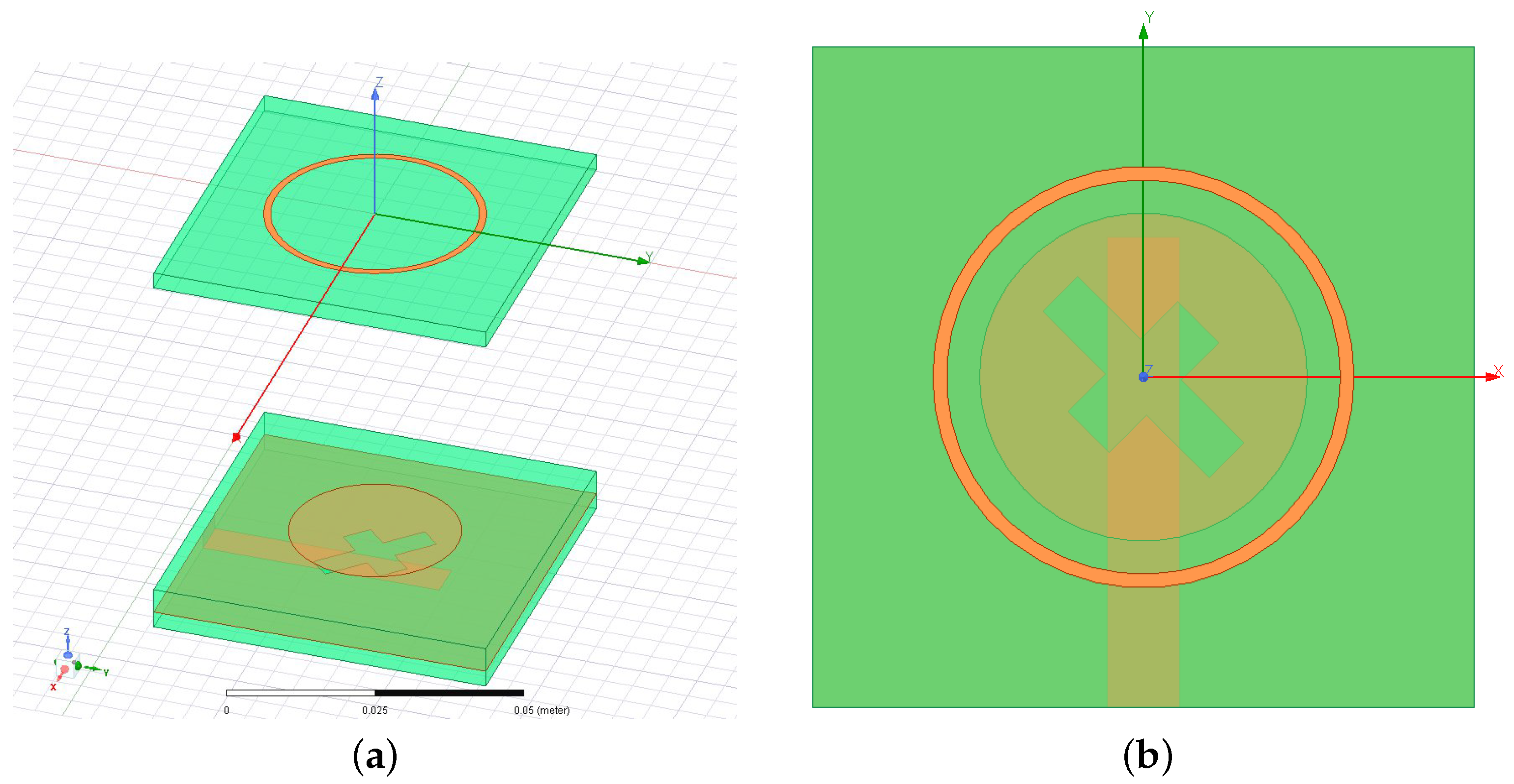
2. WWCS Antenna Layout
Figure 1 shows a geometric sketch of the layout of the proposed
WWCS radiator. The antenna lies on the
plane and it comprises
square dielectric layers
,
of side
. The thickness, the relative permittivity, and the loss tangent of the
l-th (
) layer are denoted with
,
, and
, respectively. The two stacked bottom layers (i.e.,
and
) are relative to the
primary antenna element, which consists of a circular microstrip patch of radius
, printed on the layer
[
Figure 1 and
Figure 2b]. Such a patch is fed with an aperture-coupling mechanism. Towards this end, a cross-shaped slot is etched in the ground plane that separates the layers
and
[
Figure 1 and
Figure 2a], which is in turn excited with a microstrip feeding line of width
and characteristic impedance
. This latter is printed on the bottom face of
[
Figure 1and
Figure 2a]. To maximize the
EM coupling, the microstrip line, the slot, and the patch are aligned with respect to the
plane (
Figure 1). Moreover, the feeding line is terminated into an open-circuited stub whose length
[
Figure 2a] is properly tuned so that the standing-wave current, induced within the microstrip, is maximum at the slot barycenter [
6].
It is worth pointing out that, even though a multiple-layer etching manufacturing process is required, the adopted aperture feeding enables some advantages with respect to a probe/pin-based choice [
6]. For instance, (
a) is a wide-band impedance matching, (
b) is a an easier construction, since it avoids the vertical pin that would require additional drilling and soldering processes, and (
c) is the higher polarization purity and pattern symmetry since the vertical pin would behave as an additional monopole degrading the overall axial ratio (
AR) and cross-polar discrimination (
XPD). Moreover, the use of independent substrates for both the circular patch (i.e.,
) and the feeding line (i.e.,
) gives the designer more flexibility in selecting the optimum dielectric support for each antenna “building block” with respect to a solution with coplanar edge feeding (either direct or inset-based) [
6].
As for the shape of the slot, a 45-degrees rotated cross, with unequal arms of width
(
) and length
(
) [
Figure 1 and
Figure 2a], was adopted to realize the desired circular polarization (
CP). As a matter of fact, the introduced asymmetry allows one to excite, by injecting a current into the feeding line and exploiting the aperture coupling mechanism, two orthogonal current components having a phase difference of 90 [deg] onto the patch. As a result of the combination of such excited modes, a
CP current is yielded, which in turns radiates a
CP field. More specifically, left-hand (
LHCP) or right-hand (
RHCP)
CPs are obtained by simply letting
or
, respectively [
7]. Otherwise, the polarization switching (
LHCP ⇔ RHCP) could be yielded by simply mirroring the cross aperture with respect to the
y-axis. Thanks to such a modeling, it is possible to enforce a
CP by means of a simple design and manufacturing process, since there is no need for two separate orthogonal microstrip lines. Moreover, a simple circular patch can be used by avoiding more complex solutions such as, for instance, a primary element with elliptic-shape (that would imply the tuning of the two semi-axes) or electrically-small perturbations of the external border of the patch (e.g., stubs or notches) to yield an
AR close to one [
7].
The top layer (i.e.,
) hosts the
secondary element of the antenna, which is implemented as a metallic ring of inner radius
and width
[
Figure 1 and
Figure 2c]. Such a parasitic element is “activated” by an air coupling mechanism by placing the layer
at a proper distance
D above the patch (
Figure 1). Overall, the total height of the
WWCS antenna turns out to be (
Figure 1)
The secondary passive element shares a geometric rotational symmetry with the primary active one to obtain a high polarization purity and an azimuth-invariant radiation pattern, which is a highly desirable feature for
WASAs [
11]. Indeed, by properly exciting a
CP current within the parasitic ring [
20], a torus-shaped pattern with maximum gain on the azimuth plane [i.e.,
[deg]—
Figure 1a)] is radiated. The metallic ring shape is selected to assure that the arising parasitic radiation mode triggers an increased end-fire gain. As a consequence, the combination of the field radiated by the primary element [having maximum gain at broadside, i.e.,
[deg]—
Figure 1a] and the secondary radiator generates a wide beam with half-power beamwidth close to
[deg] along every elevation plane
[deg] [
Figure 1a].
3. Design Methodology
In order to address in a computationally-effective way the synthesis problem at hand, a customized implementation of the system-by-design (
SbD) paradigm [
32] is exploited and briefly summarized in the following. More specifically, the “
Problem Formulation”
SbD functional block [
32] is customized to (
i) define a proper set of geometric descriptors of the
WWCS layout and (
ii) formulate a suitable multi-objective cost function accounting for several user-defined requirements on both impedance matching and radiation features. Concerning (
i), once the characteristics of the substrates (i.e., material/thicknesses) of the layers
,
, and the width of the microstrip feeding line
are determined as detailed in [
8] (p. 148, Equation 3.197) to yield the desired characteristic impedance
(e.g.,
[
]), the set
of geometric descriptors (
Figure 1 and
Figure 2) is defined as
,
[
] and
[
] being auxiliary parameters (
;
) that avoid the generation of physically-unfeasible geometries for the secondary element by enforcing the constraints
and
, respectively [
Figure 2c]. The synthesis problem at hand can then be stated as follows:
WWCSAntenna Design Problem—Determine the optimal setup of the degrees-of-freedoms (
DoFs),
, such that the corresponding
WWCS radiator (
i) exhibits a suitable impedance matching within the user-defined wide frequency range
, (
ii) radiates an azimuth-invariant wide-beam pattern suitable for
WASAs, and (
iii) implements a
LHCP/RHCP with high polarization purity within the half-space region
⋃
[deg] [
Figure 1a].
As for (
ii), because of the conflicting requirements on the bandwidth and the radiation features as well as the non-linear dependence of these latter on
, the original synthesis problem is recast into a global optimization one, where
being the cost function, which quantifies the mismatch with the synthesis targets, given by
where
, and
is a real weight associated with the
-th cost function term
. More in detail, the impedance bandwidth term of the cost function
(
) is defined as follows
where
is the reflection coefficient at the antenna input port,
being the input impedance. Moreover,
is the desired threshold and
[
] is the
q-th (
) frequency sample,
Q being the number of spectral components analyzed with full-wave (
FW) simulations. Finally,
is the Heaviside’s function, equal to
if
and
, otherwise.
As for the wide-beam features, the
HPBW cost term (
) is given by
where
is the user-defined requirement, while
(
[deg]) is the
m-th (
) azimuth angular sample [
Figure 1a],
M being the number of elevation planes considered for the numerical evaluation of the
HPBW.
The last two cost function terms in (
3) (i.e.,
and
) are related to the
CP and they are defined as follows
and
In the previous expressions,
[deg] is the
v-th (
) elevation angle [
Figure 1a],
is the maximum
AR given by [
6]
where the subscripts “
” and “
” denote the co-polar and the cross-polar field components, respectively (i.e.,
and
if a
LHCP antenna is designed, and vice-versa for
RHCP operation), equal to
being the far-field electric field,
is the dot product, and
stands for complex conjugate. Moreover,
and
are the polarization unit vectors for the two
CPs [
6]
Finally,
is the minimum
XPD being
where
is the gain related to the
/
-th field component, respectively,
is the free-space impedance, while
is the accepted power at the antenna terminals for a given incident power
The overall
SbD-driven design work-flow consists of the following procedural steps:
Input phase. Define the bounds of the target’s operating band, and , the required CP (i.e., LHCP or RHCP), and the threshold value for each key performance indicator, . Perform the following operations
- (a)
Set , being the free-space impedance at the central frequency ;
- (b)
Select from an off-the-shelf data-sheet the material/thickness of the l-th () layer ;
- (c)
Compute the width of the feeding line
to yield the desired characteristic impedance
(p. 148, Equation 3.197 [
8]);
- (d)
Derive an analytic guess,
, for the radius of the primary element of the radiator as detailed in [
33] (p. 846, Equation 14.69), then set its optimization range
and
as a percentage of
, being
;
- (e)
Define the optimization bounds of the remaining DoFs , ;
Surrogate model (SM) Building. Use the Latin hypercube sampling (
LHS) strategy [
32] to generate a training set
of
training samples,
being the cost function associated with the
s-th (
) input sample
, computed with a
FW simulation. Starting from
, build a computationally-fast
SM of (
3) based on the ordinary Kriging (
OK) learning-by-examples (
LBE) technique [
32,
34,
35,
36,
37];
Design Initialization ()—Define an initial swarm of P particles, , with random velocities ;
SbD Design Loop (
)—Iteratively update the swarm positions and velocities by applying the
PSO-OK/C updating rules [
32],
, and leveraging on both the cost function predictions and the associated “reliability estimations” outputted by the
SM. As for the latter, the training set at the
i-th (
) iteration,
, of size
, comprises progressively-added training samples according to the
SbD “reinforcement learning” strategy [
32] aimed at refining the prediction accuracy within the attraction basin of
;
Output Phase—Output the final setup of the DoFs, , whose corresponding layout best fits all user-defined requirements.
4. Numerical Assessment
This section is aimed at illustrating the performance of the proposed
WWCS antenna model. Towards this end, the synthesis of a
LHCP-polarized radiator working in the
[GHz] band (⇒
[GHz] and
[mm] [
20]) was addressed. The Rogers RO4350B substrate was chosen for the
layers (
,
,
) with thicknesses set to
[mm] and
[mm]. According to [
8], the width of the microstrip feeding line turns out to be
[mm] for
[
], while the analytic guess of the patch radius is set to
[mm] [
33]. The
PSO-OK/C parameters were chosen by following the literature guidelines to yield a time saving of
with respect to a standard optimization based on a bare integration of the global optimizer and the
FW simulator to compute the cost function values in correspondence with each trial antenna layout [
32].
More specifically, the swarm size, the number of iterations, the social/cognitive acceleration coefficients, the inertial weight, and the initial training size were set to
,
,
,
, and
, respectively. Moreover, the numerical evaluation of (
3) was performed by sampling into
,
, and
samples the frequency, the azimuth, and the elevation range, respectively, while letting
[dB],
[deg],
[dB], and
[dB]. Finally, the optimization bounds were set to
,
,
,
,
, and
.
The geometric descriptors of the
SbD-optimized layout are reported in
Table 2, while the corresponding layout, modeled in the Ansys
HFSS FW simulator [
38] and having an overall height of
[mm] (
[
] —
Table 1), is shown in
Figure 3. Going to the analysis of the antenna performance,
Figure 4 shows the simulated reflection coefficient at the antenna input port versus the frequency. As it can be observed, such a radiating element fully complies with the requirement since
[dB] for
.In more detail, it turns out that
for an even wider frequency interval (
[GHz]) by assessing the wide-band behavior of the proposed design with an overall fractional bandwidth of
[
39], while, for instance, the state-of-the-art solution in [
20] is limited to
(
Figure 4 and
Table 1).
As for the radiation features,
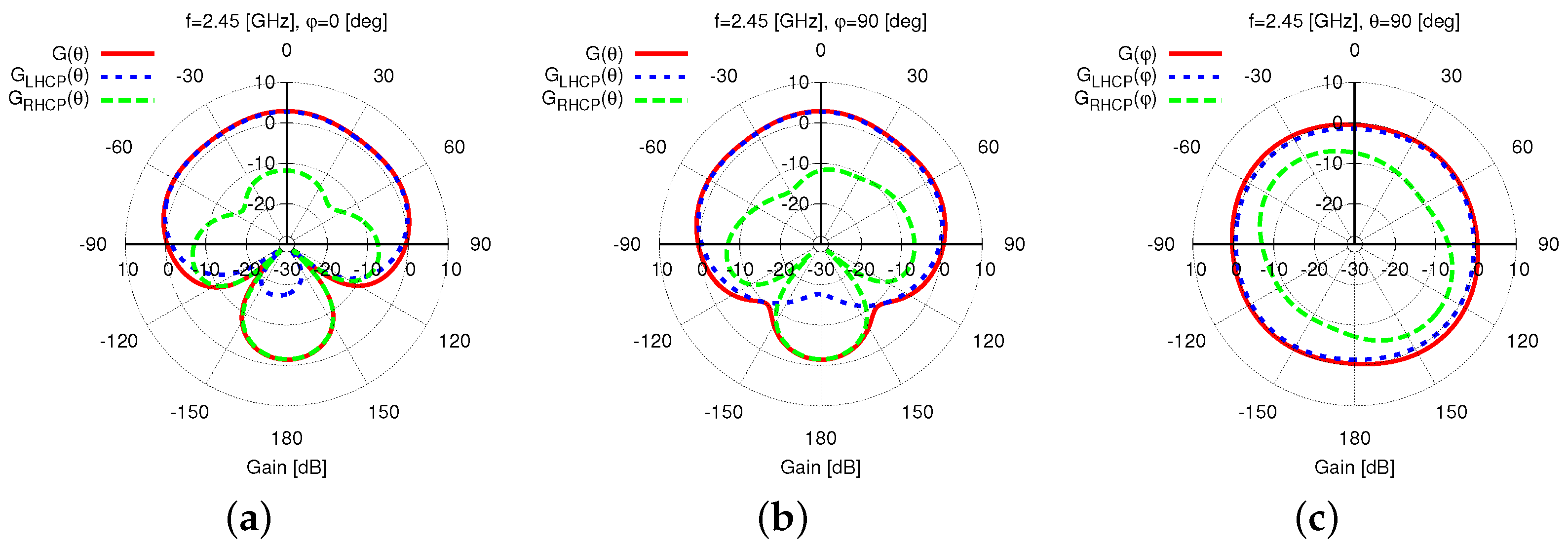
Figure 5 shows the gain pattern at
,
, along the two main elevation planes [i.e.,
[deg]—
Figure 5a and
[deg]—
Figure 5b] and the azimuth plane [i.e.,
[deg]—
Figure 5c]. Since the
HPBW is equal to
[deg] [
Figure 5a] and
[deg] [
Figure 5b] on the two vertical cuts, with a good pattern omni-directionality of the whole antenna horizon [
Figure 5c], it is reasonable to indicate the proposed antenna such as a wide-beam one suitable for implementing
WASAs. It is worth noticing that such a feature has been yielded thanks to the constructive combination of the fields radiated by the primary and secondary sources. To better illustrate the
EM phenomena and interactions,
Figure 6 shows the 2D plot of the magnitude of the electric field,
, on a vertical surface parallel to the
-plane and crossing the barycenter of the antenna. As it can be observed, the air coupling between the bottom (primary) and the top (secondary) element of the radiator at hand guarantees a proper excitation of the parasitic element by enabling the generation of a wide beam in the far-field region. The wide-beam behavior of the synthesized
WWCS antenna in a wide frequency is “detailed” in
Figure 7a,b, where the two elevation gain patterns at
frequencies
,
are given. The remarkable stability, also in frequency, of the wide-beam radiation is pointed out by the plot of the
HPBW versus the frequency being
[deg] and
[deg] for
[
Figure 7c]. To better understand the advantages of the proposed design, the behavior of the
of a planar radiator obtained by removing the top layer (i.e.,
—
Figure 1) is shown as well [
Figure 7c]. It turns out that the presence of the parasitic ring in the synthesized
WWCS radiator (
Figure 1) almost doubles the
at the central frequency, thus verifying its effectiveness in yielding a wide-beam behavior [
Figure 7c].
The optimized
WWCS layout exhibits the desired
LHCP operation and is pointed out by both the co-polar,
, and the cross-polar,
, gain patterns in
Figure 5, where it can be clearly observed that
and
for
[deg] with broadside
AR and
XPD equal to
[dB] and
[dB], respectively. Moreover, such a good polarization purity is kept almost unaltered in the complete radiating upper semi-sphere with the exception of the elevation angles close to the antenna end-fire as illustrated by the 2D maps of
[
Figure 8a] and
[
Figure 8c] as well as by the corresponding thresholded pictures aimed at highlighting the fulfilment of the design requirements [
Figure 8b,d]. It is worth remarking that the slight degradation of both
AR and
XPD appears only in the most challenging region (i.e.,
[deg]) and is possibly due to the spurious radiation by the slot along the directions of its major arms (i.e.,
[deg] and
[deg]—
Figure 8 and
Figure 3).
In order to assess the excitation of a
LHCP, the plot of the magnitude of the instantaneous surface current density,
, is reported in
Figure 9 at four consecutive instants [i.e.,
[sec]—
Figure 9a;
[sec]—
Figure 9b;
[sec]—
Figure 9c;
[sec]—
Figure 9d
being the period at
,
]. One can observe that the fundamental mode
is properly excited on the circular patch [
33] and there is a clock-wise rotation of the corresponding surface current distribution (
Figure 9). The vector plot of the electric field distribution at a quota of
,
, shown in
Figure 10 for the same instants, further verifies the desired
CP of the radiated wave, which evolves in time according to a
LHCP.
For comparison purposes,
Figure 11 plots the broadside gain
[
Figure 11a] and the
AR [
Figure 11b] within the band of interest of the proposed
WWCS model and of the design in [
20]. It turns out that the synthesized radiator exhibits a good
AR performance, especially within the band
[GHz] where
[dB] [
40], that results in an
AR bandwidth (
ARBW) equal to
, while
[i.e., an improvement by
times—
Figure 11b]. A similar outcome is yielded for the 3 [dB]-bandwidth, as well, since
and
[i.e., an improvement by
times—
Figure 11b].
Finally, the suitability of the
WWCS radiator as elementary building block of circularly-polarized wide-band
WASAs was assessed. Towards this end, the radiation features of a large planar uniform phased array, comprising
WWCS identical elementary radiators, were studied. To account for the mutual coupling in this large aperture, a periodic model was simulated in
HFSS.
Figure 12a) describes the behavior of the array gain along the angular steering direction,
, when setting uniform phase shifts and isophoric excitations to scan the beam in the range
[deg] in both vertical planes (i.e.,
[deg] and
[deg]).To avoid the insurgence of grating lobes for close-to-endfire operation, an inter-element spacing of
[
] was chosen by slightly shrinking the side of the
WWCS antenna to
.
Thanks to the wide-beam nature of the
WWCS elementary radiator, the array exhibits good scan loss (
SL) performance [
], as illustrated by the patterns at different values of the scan angle
for both
[deg] [
Figure 12b] and
[deg] [
Figure 12c]. The
SL on both elevation planes is always smaller than
[dB] at the central frequency [
Figure 12a]. Moreover, it is worth noticing that there is a good stability of the sidelobe level (
SLL) when scanning the beam on both planes [i.e.,
[dB]—
Figure 13a].
Similar outcomes can be inferred for the array
HPBW as well, since
[deg] for
[deg], while it rapidly increases outside such an angular interval because of the beam broadening effect [
33] [i.e.,
[deg] for
[deg]—
Figure 13a and [
Figure 12b,c]. Moreover, a good polarization purity is yielded in the whole scan range as indicated by the plot of both the
AR and the
XPD along the angular steering direction, since
[dB] and
[dB] when
[deg] and
[deg] [
Figure 13b]. Finally, let us note that the
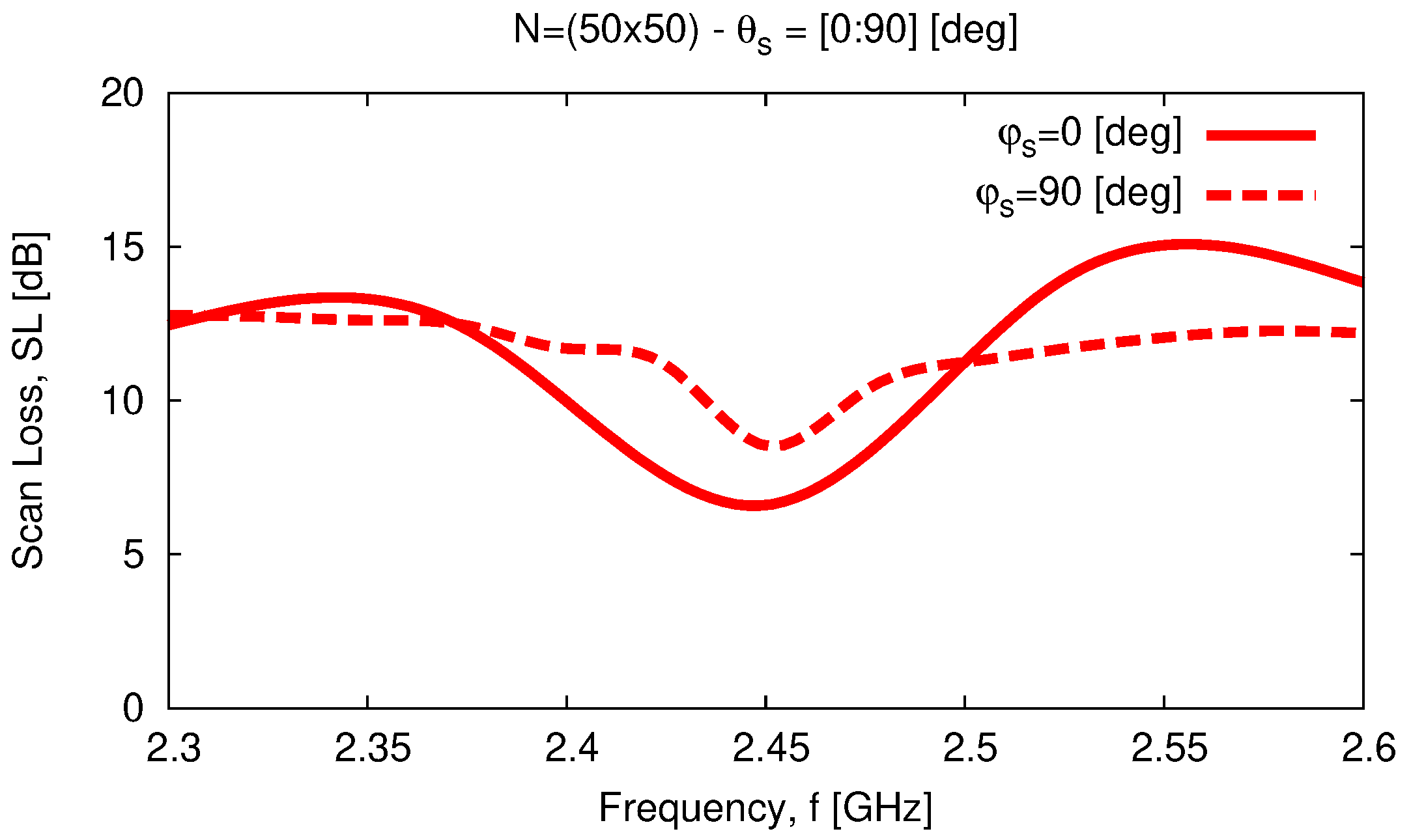
WASA properties of the array are confirmed within the frequency range of interest (
Figure 14) where
[dB] for
in both elevation planes.
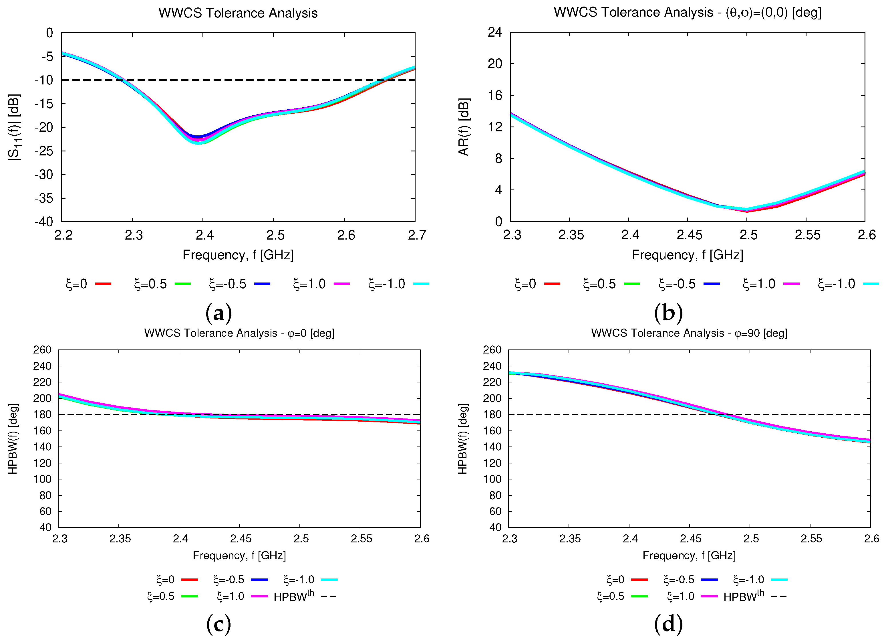
In addtion to the numerical assessment, a tolerance analysis has been carried out to give the interested reader some insights into the reliability and robustness on the fabrication tolerances of the proposed antenna layout both stand-alone and within an array arrangement. First, the height of the parasitic element,
D, has been supposed to deviate of
and
from the nominal value
(Tab. II) because of some manufacturing tolerances.
Figure 15 summarizes the results of the tolerance analysis versus the frequency for the input reflection coefficient [
Figure 15a], the broadside
AR [
Figure 15b], and the
HPBW along the
[deg] [
Figure 15c] and the
[deg] [
Figure 15d] planes. As it can be inferred, the proposed antenna layout turns out to be quite robust. More precisely, the wide-band [
Figure 15a] and the wide-beam [
Figure 15c,d] characteristics of the
WWCS radiator are confirmed regardless of the non-negligible fabrication tolerances on
D, the fractional bandwidth being equal to
in the worst case [i.e.,
—
Figure 15a]. As a consequence, the scan loss value of the array,
, within the working frequency range,
, is quite stable in both elevation planes (
Figure 16), as well.
Similar conclusions can be drawn when taking into account fabrication tolerances on the width of the feeding line,
, and the parasitic ring,
, which have been varied according to the following rule:
,
[
m] being the metallization thickness and
. The effects of such deviations are almost negligible on the features of both the elementary radiator and the array as one can derive from the analysis of the plots in
Figure 17 and in
Figure 18, respectively.
5. Experimental Assessment
The experimental validation of the performance of the designed
WWCS has been carried out next (
Figure 19). In order to exploit available off-the-shelf RO4350B
PCB boards, two (layers
and
—
Figure 1) and three (layer
—
Figure 1) substrates of thickness
[mm] have been stacked to realize the different layers of the antenna. The overall structure has been assembled using four nylon
M4 threaded rods and sixteen nylon bolts, stacking together the
PCBs and placing the parasitic ring at distance
from the driven patch (
Figure 19). An
RS 759-5252 SMA connector has been used to feed the antenna prototype.
Figure 20 shows the measured reflection coefficient at the input port of the antenna under test (
AUT) by employing a properly calibrated scalar network analyzer Rohde & Schwarz ZVH4 (100 [kHz]—3.6 [GHz]). As it can be seen, the fabricated
WWCS exhibits a suitable impedance matching in the complete target band, being
[dB] and
[dB]. Moreover, a slightly larger bandwidth has been observed with respect to the
HFSS simulation (i.e.,
—
Figure 20).
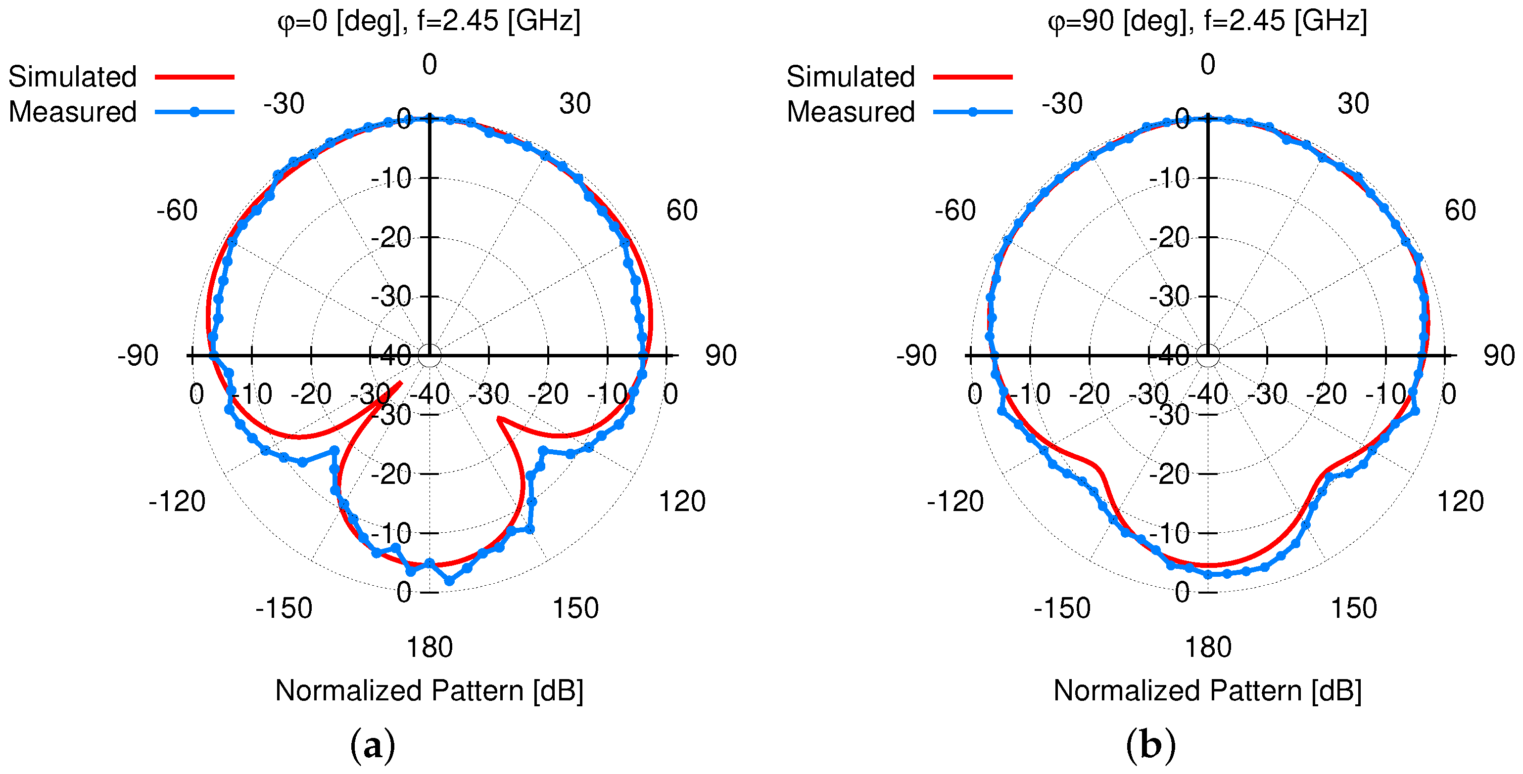
As for the radiation features of the fabricated antenna, the far field patterns have been measured inside an anechoic chamber having dimensions
[
]. The
AUT has been placed on a remotely controlled rotating frame and the electric field has been measured by means of a circularly polarized probe connected to a signal analyzer, both placed on a dielectric mast at a distance of 3 [m] from the
AUT. In order to avoid field perturbations due to cablings, the
AUT has been connected with a short coaxial cable to a small transmitter able to generate a constant amplitude and frequency signal at
[GHz]. The transmitter has been placed just behind the layer
of the
AUT. Similarly, the presence of a long coaxial cable connected to the field probe has been avoided thanks to the use of the PMM 9060 EMI Receiver/Signal Analyzer (30 [MHz]–6 [GHz]) that can be remotely controlled by means of a fiber optic link. A good matching between the simulated and measured gain pattern has been obtained. As a matter of fact, both pattern cuts along the
[deg] [
Figure 20a] and the
[deg] [
Figure 21b] elevation planes closely match the outcomes of the numerical assessment. Moreover, it turns out that the measured
HPBW verifies the wide-beam behavior of the radiator on both planes, being
[deg] [
Figure 21a] and
[deg] [
Figure 21b], respectively. Finally, the measured gain,
AR, and
XPD are equal to
[dB],
[dB], and
[dB], respectively, thus verifying a good matching with the simulated values.
6. Conclusions
The design of a novel wide-band wide-beam circularly-polarized elementary radiator has been proposed for
WASAs. Such a
WWCS structure leverages on a cross-shaped aperture-coupling feeding mechanism to achieve wide-band
LHCP/RHCP operation using a simple circular patch and a single microstrip line. Moreover, it takes advantage of the air coupling between the primary and secondary
EM sources to realize rotational-symmetric patterns with large elevation
HPBWs and high polarization purity in the complete upper semi-sphere. The computationally-efficient synthesis of the layout of the
WWCS antenna, which supports the desired
CP operation, has been carried out with a customized implementation of the
SbD paradigm. Accordingly, the main advancements with respect to the state-of-the-art [
20] include (
i) the exploitation of an aperture feeding mechanism instead of a probe feeding to significantly widen the impedance bandwidth, mitigate spurious radiation, and enable an easier manufacturing, (
ii) the formulation of the design problem as a global optimization one rather than a parametric
trial-and-error approach, enabling to better control the
AR and the
XPD in the complete radiating semi-sphere, (
iii) the study over a wide-band of the radiation features of the resulting planar array, as well as (
iv) the fabrication tolerance analysis on both single element and array performance.
The numerical results, concerned with the representative design of a WWCS radiator working at the central frequency of [GHz], have demonstrated that the proposed radiating structure provides
wide-band fractional impedance bandwidth (
), which is
times larger than that in state-of-the-art solutions based on similar
EM mechanisms [
20];
wide-beam radiation pattern with
[deg] in all elevation planes (versus
[deg] of [
20]);
high polarization purity with broadside
[dB] and
[dB], together with a 3 [dB]
AR bandwidth 12 times larger than [
20].
As for the arising WASA, the numerical assessment has pointed out the potential of the proposed layout of the elementary radiator for the realization of wide-band circularly-polarized WASAs. Finally, the reliability and robustness on the fabrication tolerances of the proposed antenna layout have been verified for both the stand-alone and the array arrangement.
Furthermore, the experimental assessment of a
PCB-manufactured prototype has verified the
FW-simulated outcomes, confirming both the wide-band and the wide-beam features of the designed
WWCS radiator (
Figure 20 and
Figure 21).
It should be pointed out that the proposed design concept and methodology are general since they can be applied to synthesize wide-band wide-beam CP radiators working in different operative bands. Indeed, the designer is given the freedom to choose the materials of the different layers as well as the desired target performance (i.e., bandwidth, HPBW, AR, and XPD) for the specific applicative scenario at hand.
Future works, beyond the scope of the current manuscript, will be aimed at assessing the possibility to exploit the stripline technology to feed the antenna and at investigating the resulting advantages and drawbacks.

 ,
, 


