Article

A Multimode 28 GHz CMOS Fully Differential Beamforming IC for Phased Array Transceivers

1
Department of Electronic Engineering, Kwangwoon University, Seoul 01897, Republic of Korea
2
Department of Information Technology and Electrical Engineering, ETH, 8092 Zurich, Switzerland
3
School of Electrical Engineering, Chung-Ang University, Seoul 06974, Republic of Korea
*
Author to whom correspondence should be addressed.
Sensors 2023, 23(13), 6124; https://doi.org/10.3390/s23136124
Submission received: 19 May 2023 / Revised: 28 June 2023 / Accepted: 1 July 2023 / Published: 3 July 2023
(This article belongs to the Special Issue Advanced CMOS Integrated Circuit Design and Application II)

Abstract

:
A 28 GHz fully differential eight-channel beamforming IC (BFIC) with multimode operations is implemented in 65 nm CMOS technology for use in phased array transceivers. The BFIC has an adjustable gain and phase control on each channel to achieve fine beam steering and beam pattern. The BFIC has eight differential beamforming channels each consisting of the two-stage bi-directional amplifier with a precise gain control circuit, a six-bit phase shifter, a three-bit digital step attenuator, and a tuning bit for amplitude and phase variation compensation. The Tx and Rx mode overall gains of the differential eight-channel BFIC are around 11 dB and 9 dB, respectively, at 27.0–29.5 GHz. The return losses of the Tx mode and Rx mode are >10 dB at 27.0–29.5 GHz. The maximum phase of 354° with a phase resolution of 5.6° and the maximum attenuation of 31 dB, including the gain control bits with an attenuation resolution of 1 dB, is achieved at 27.0–29.5 GHz. The root mean square (RMS) phase and amplitude errors are <3.2° and <0.6 dB at 27.0–29.5 GHz, respectively. The chip size is 3.0 × 3.5 mm2, including pads, and Tx mode current consumption is 580 mA at 2.5 V supply voltage.

1. Introduction

The increasing demand for data communication brings about the emergence of 5G communications using mm-wave technology. Mm-wave phased array transceivers support multiple users operating with high data rates using broadband directional links between the mm-wave base stations and mobile devices [1,2,3,4,5,6,7]. To overcome the high free-space path losses at mm-wave frequencies, a phased array antenna has become one of the key techniques for mm-wave 5G communications. Therefore, RF transceivers must use a phased array design incorporating beamforming and beam-steering capabilities. However, realizing a compact and low-cost phased array architecture is a major concern [8,9,10]. Currently, to satisfy the demands for high-output power and low-noise performance, the front-end modules (FEM), power amplifiers, and low-noise amplifiers are designed using GaAs or GaN. However, other sub-blocks, such as driving amplifier, variable gain amplifier, phase shifter, attenuator, and power divider, are implemented using a CMOS due to its low cost, high integration, and efficient production capabilities. This results in the number of elements and system size increase. Consequently, the BFIC is realized with the CMOS technology to achieve a balance between performance and system compactness. In this work, a multimode BFIC is presented, which has the capability to operate in multimode within a single IC. The BFIC can support a number of antennas allowing wide flexibility in optimization and improving the beam steering, beam pattern, and SNR. In order to make the compact chip size and to improve the performance of phased array transceivers, multiple channels are integrated into a single chip. As the number of channels are integrated in the single BFIC, a fully differential structure is implemented to improve the isolation at each multi-channel port as well as to reduce the coupling effects.
In this paper, a multimode 28 GHz CMOS fully differential eight-channel BFIC is presented for a phased array transceiver. The BFIC incorporates a differential SPDT switch, which enables multimode operations. It has the capability to operate in 8Tx and 8Rx modes separately as well as in a combined 8Tx8Rx TDD mode. Furthermore, it is capable of operating in the four-channel mode, allowing the independent operation of 4Tx and 4Rx within a single BFIC. This flexibility in operation modes offers a range of choices depending on the specific requirements of the number of antennas. The eight-channel mode can integrate the number of antennas, resulting in a narrow beam, high EIRP, and improvement in the SNR suitable for mm-wave base stations. Furthermore, the ability of the BFIC to support a four-channel mode enhances its suitability for mobile devices by providing a compact and power-efficient chip solution.

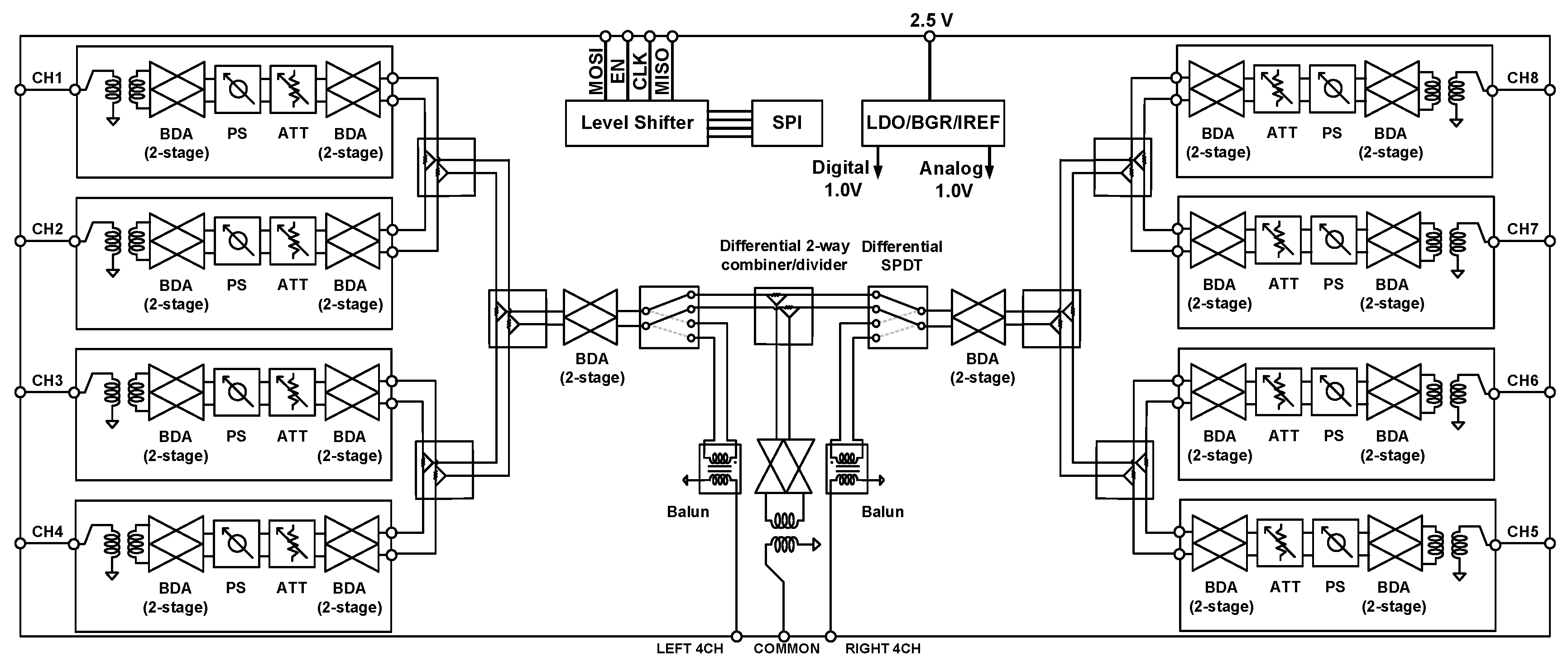
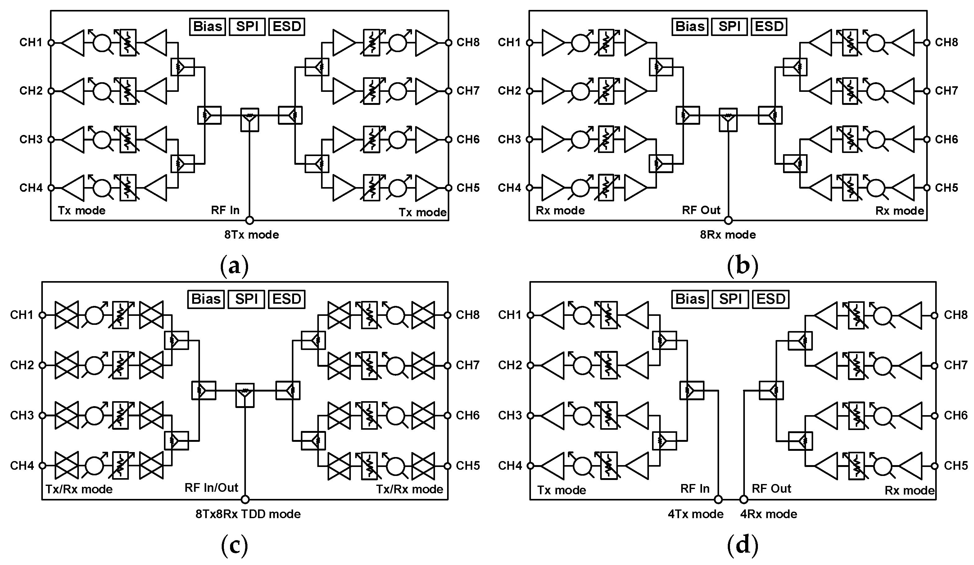
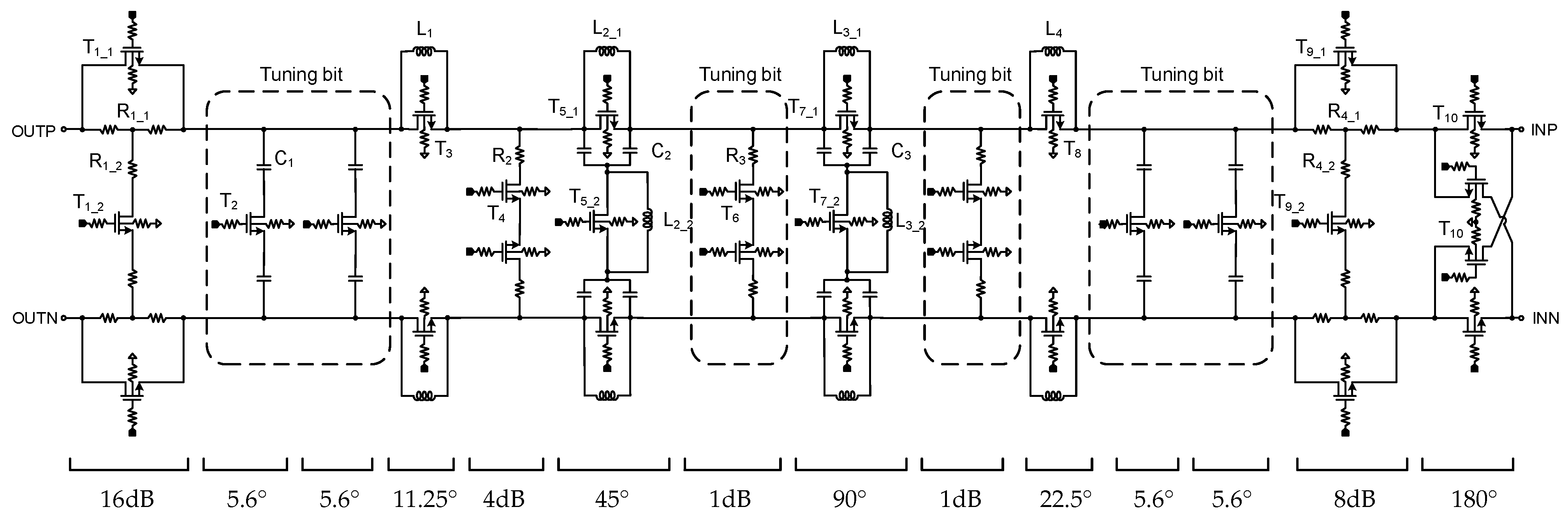
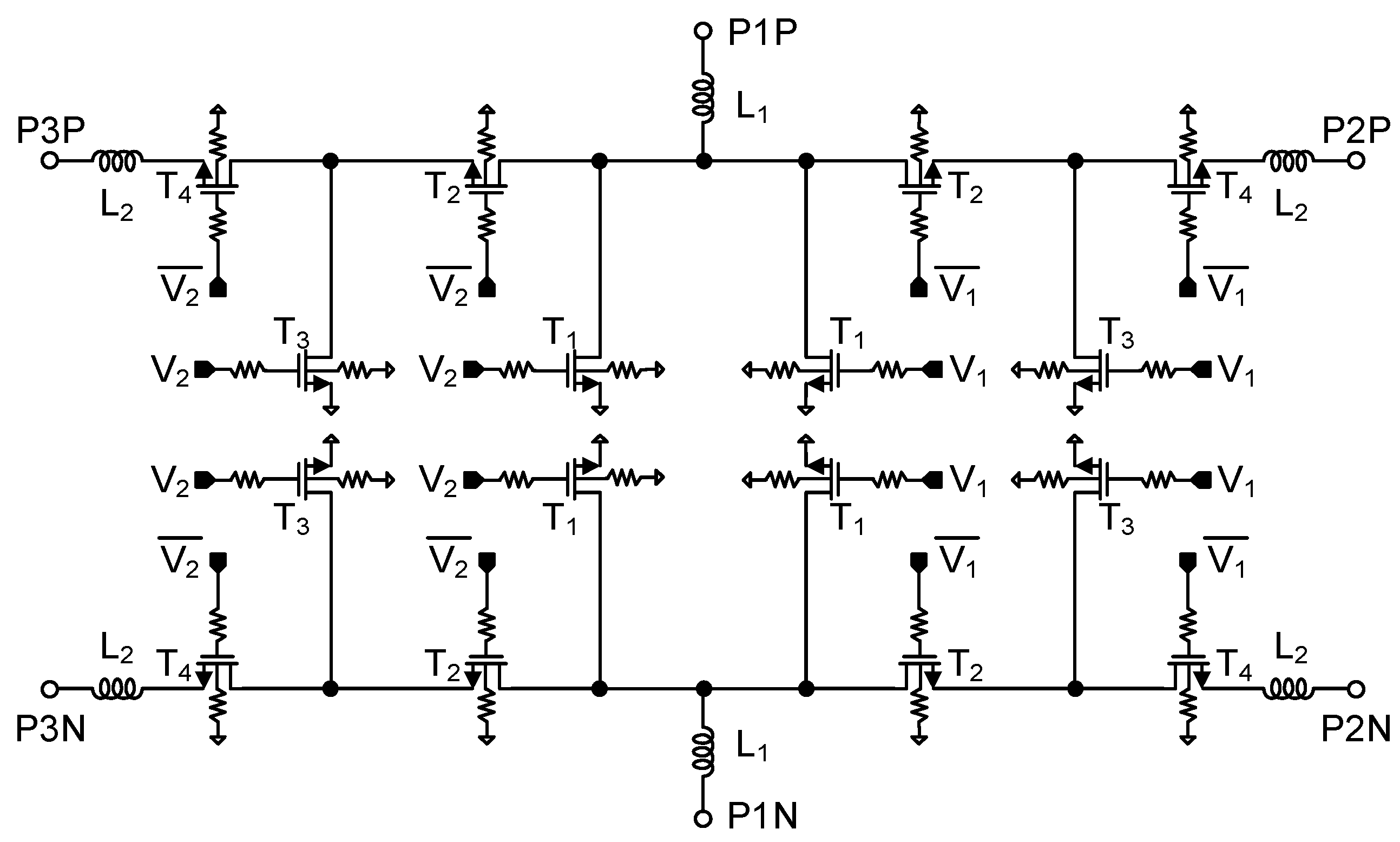
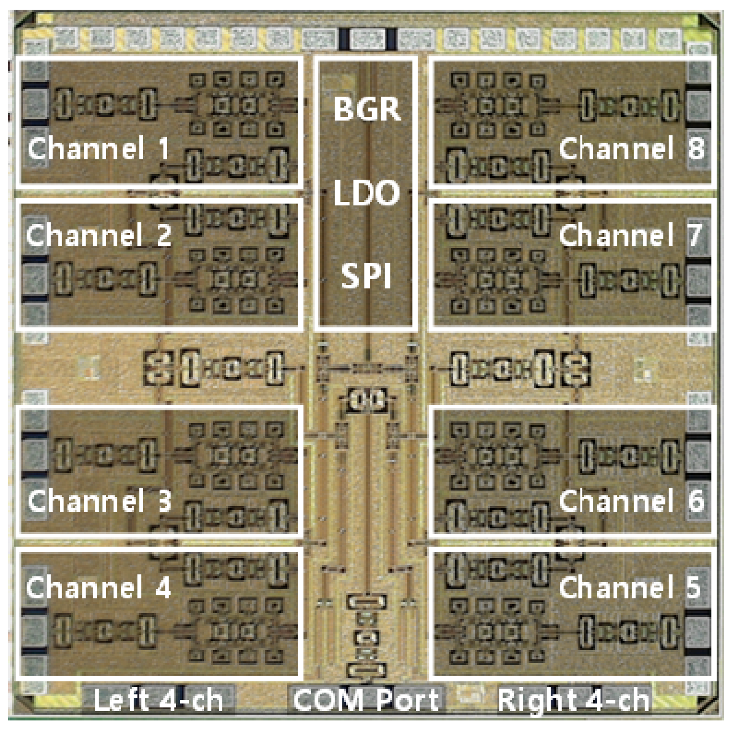
2. Design of 28 GHz Eight-Channel Multimode Beamforming IC

The RF-phase-shifting beamforming architecture has been adopted considering the power consumption, chip size, and design complexity. The block diagram of the 28 GHz eight-channel CMOS fully differential multimode BFIC is shown in Figure 1. All the circuits in the chip have a differential structure. A differential design reduces coupling between the channels and improves isolation. A simple and high-performance unit channel structure is used. Each channel consists of a differential two-stage bi-directional amplifier, a six-bit phase shifter, and a three-bit digital step attenuator. The multiple channel Tx/Rx signals are split or combined using a two-way power divider. The fully differential SPDT switch is implemented to control the multimode operations. The bi-directional amplifiers were distributed to deliver enough power to each channel. A Marchand balun is implemented in the common signal path of the four-channel for transforming single-ended and differential signals. To realize the compact phased array antenna system, the bi-directional architecture is employed. The area reduction is realized by sharing the passive phase shifters, attenuators, and power divider between the TX mode and the RX mode.
The 28 GHz eight-channel BFIC has the capability to operate in multimode, including the 8Tx and 8Rx modes separately, the 8Tx8Rx TDD mode, and also the 4Tx and 4Rx mode independently. When the SPDT switches are in the default state (off state) and all the eight-channel are set to Tx mode, it operates in 8Tx mode, as shown in Figure 2a. When all the eight-channel are set to Rx mode, then it operates as the 8Rx mode, as in Figure 2b. Additionally, by controlling the Tx/Rx mode select switches presented in each channel, it can be operated bi-directionally, which enables BFIC to be operated in the 8Tx8Rx TDD mode, as shown in Figure 2c. The BFIC is also able to operate in the four-channel mode. When the SPDT switches are on, the right side, the four-channel can be made to work in Tx mode and the left side four-channel can be made to work in Rx mode, as shown in Figure 2d. Hence, the BFIC can operate in the 4Tx and 4Rx mode independently. The bias, phase, and amplitude controls for each channel are digitally controlled by the SPI. Furthermore, the bandgap voltage reference (BGR), low drop output (LDO) regulator, and electrostatic discharge (ESD) protection circuits are integrated into the eight-channel BFIC to provide a stable DC bias.

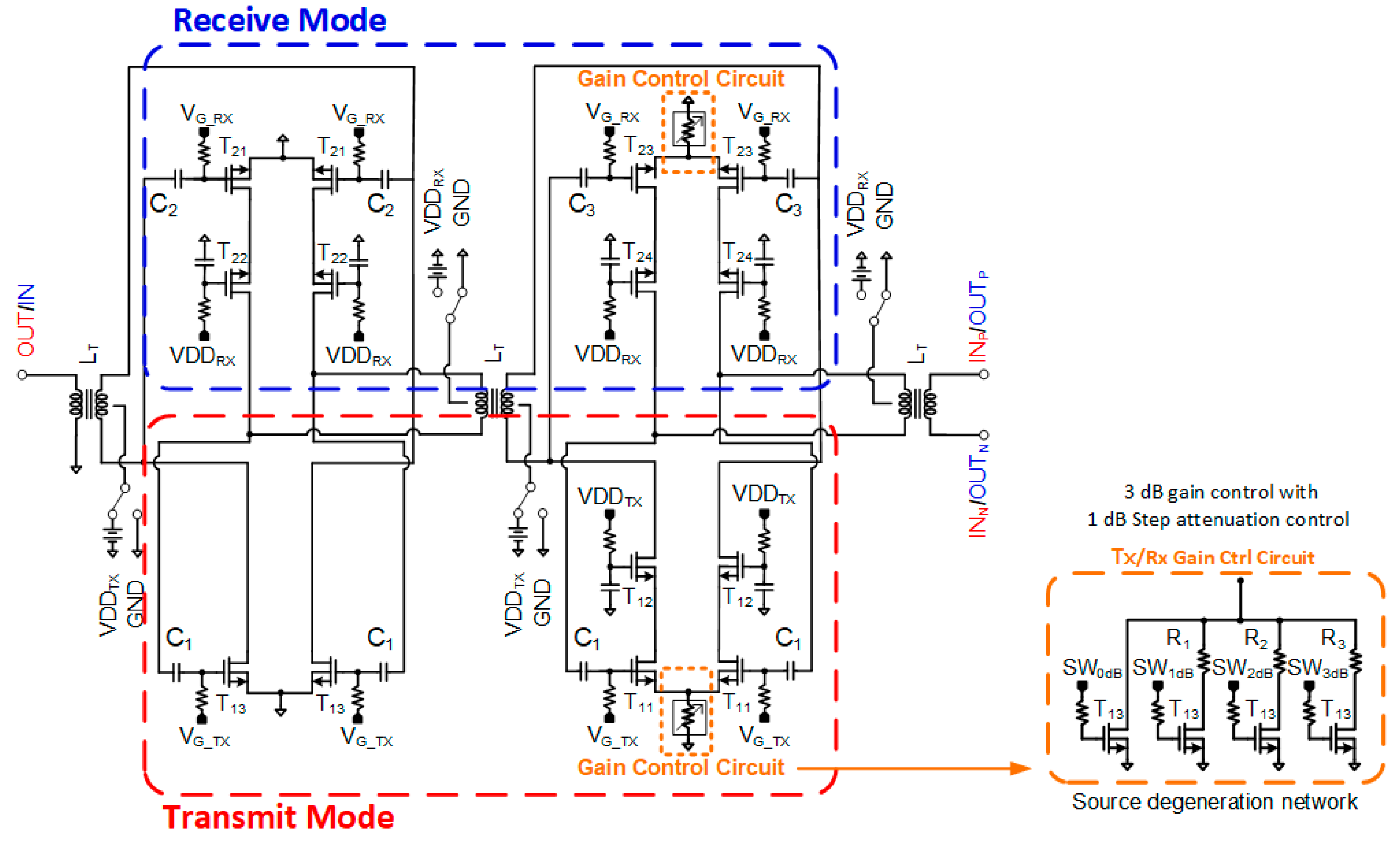
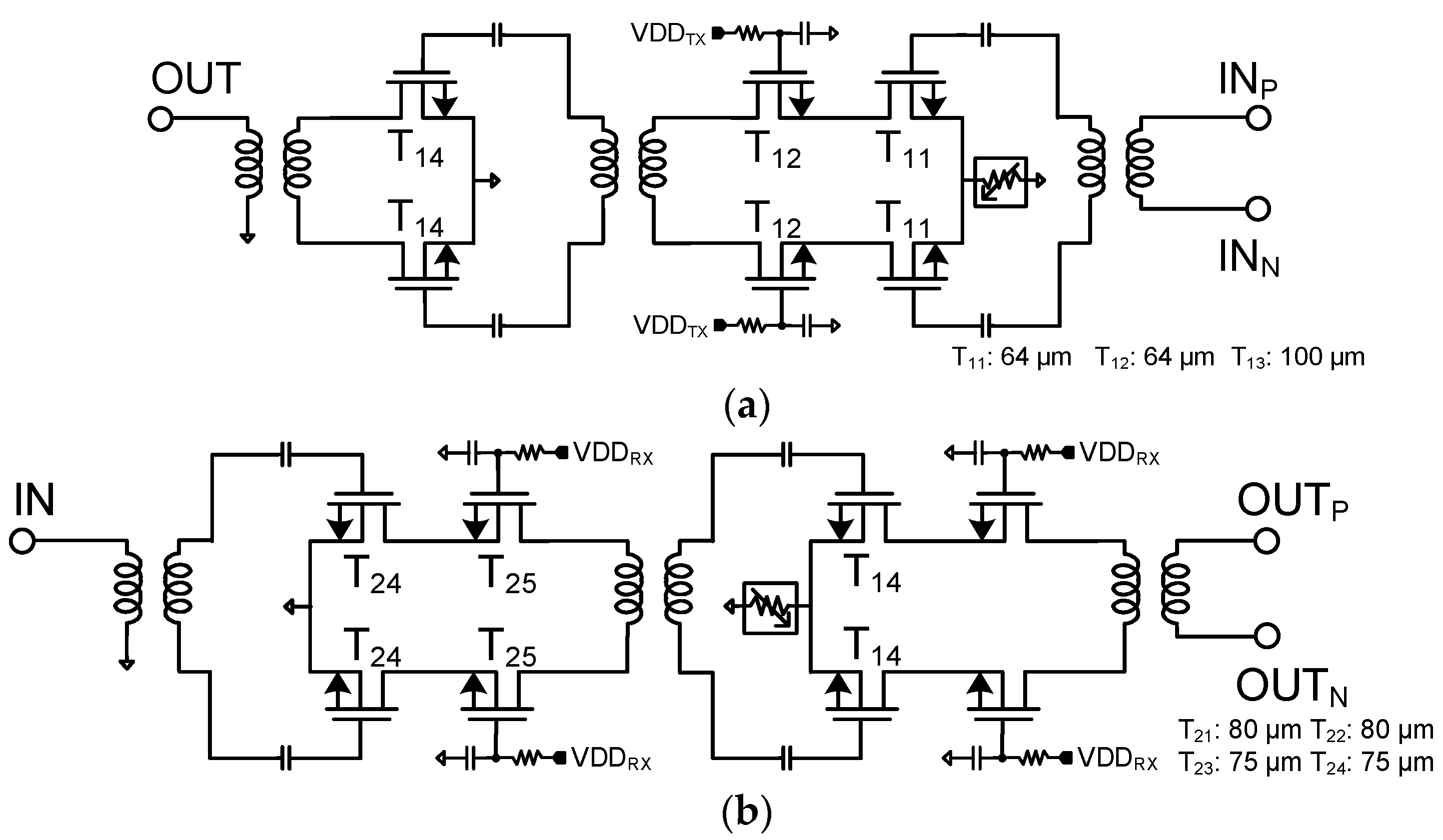
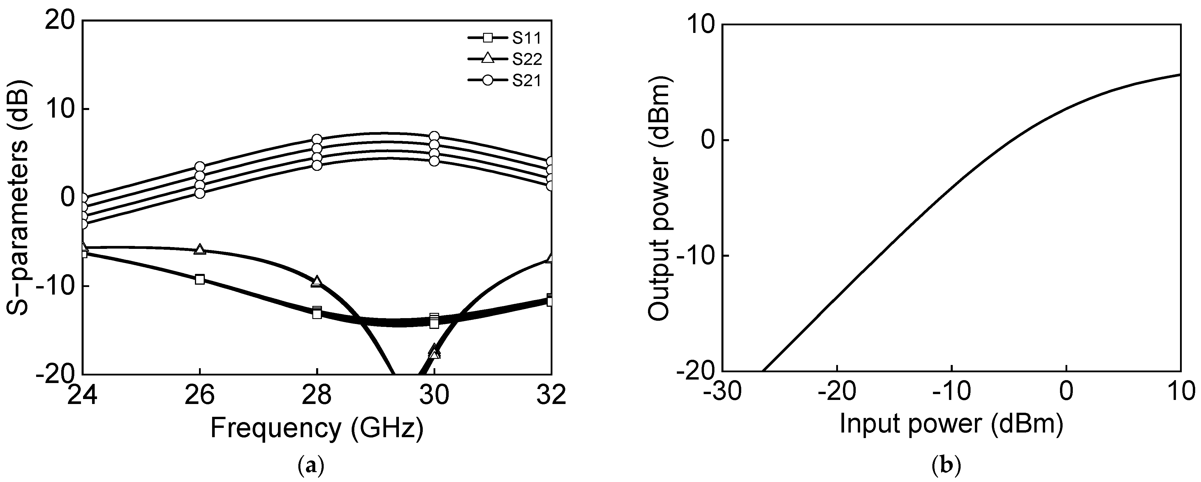
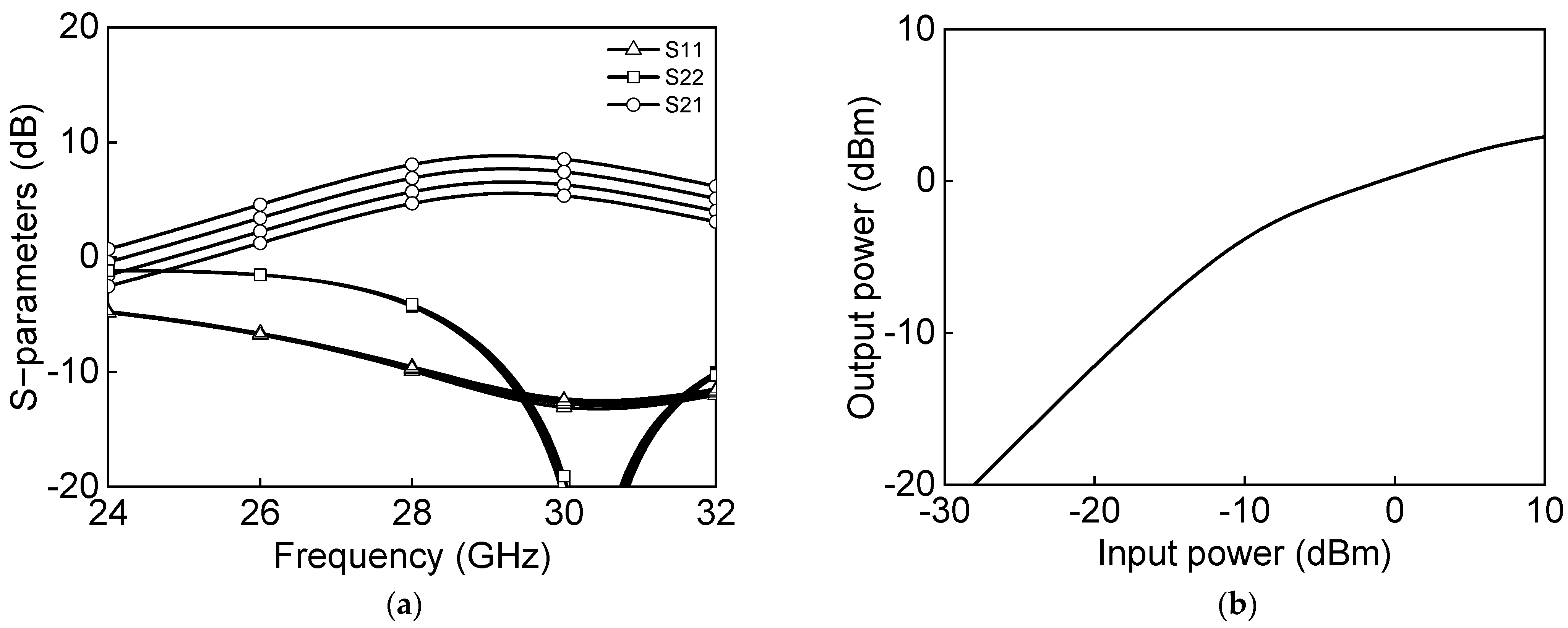
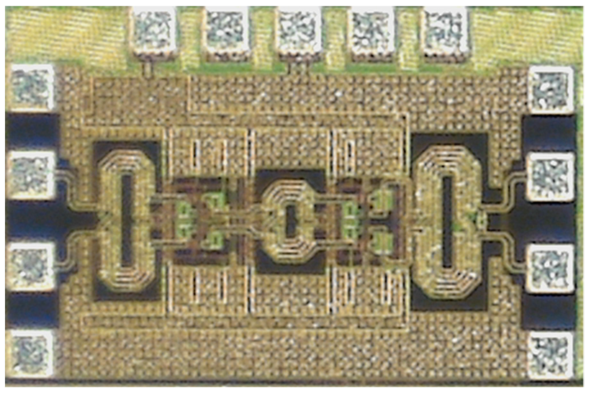
2.1. Differential Two-Stage Bi-Directional Amplifier

The differential amplifier is designed with a transformer-coupled structure, which has the advantage of not requiring a DC-blocking capacitor and RF choke and also improves the bandwidth [11]. Figure 3 shows the circuit schematic of the transformer coupled differential two-stage bi-directional amplifier. The two-stage bi-directional amplifier uses transformers for input, inter-, and output stage matching. The Tx/Rx mode select switches are used to control the Tx and Rx mode at each channel. For the Tx mode operation, transistors, T11, T12, T13, are turned on, while the Rx mode transistors, T21, T22, T23, T24, are turned off and vice-versa in the Rx mode operation. Both the Tx mode and the Rx mode gain stages are designed with cascode amplifier topology with the source degenerative resistive circuit for precise gain control. A gain control of 3 dB with 1 dB step attenuation is implemented. The gain control circuit consists of four RF NMOS transistors and the attenuation resistor. The resistances of 1 dB, 2 dB, and 3 dB attenuation are 4 Ω, 9 Ω, and 14 Ω, respectively.
The equivalent circuit diagram of the Tx mode of the bi-directional amplifier is shown in Figure 4a. The Tx mode output stage is designed with common-source topology for high linearity. Figure 4b shows the Rx mode of the bi-directional amplifier. The Rx mode input stage is designed with cascode amplifier topology for high isolation between the input and the output ports. The proposed circuit configuration does not need additional SPDT switches for bi-directional operation, which reduces the chip area as well as insertion loss in the Tx and Rx modes. Furthermore, the inductors can be shared for both modes, resulting in the reduction of inductors.
Figure 5a shows the simulated s-parameter results, and Figure 5b shows the power characteristics measurement of a differential two-stage bi-directional amplifier in the transmit mode. The transmitter-mode reference gain is 6.6 dB and output P1dB, and saturation power PSAT are −2.2 dBm and 5.6 dBm at 28 GHz. Figure 6a shows the simulated s-parameter results, and Figure 6b shows the power characteristics measurement of a differential two-stage bi-directional amplifier in the receive mode. The receiver-mode reference gain is 8.1 dB, and output P1dB and saturation power PSAT are −5.9 dBm and 2.8 dBm, respectively, at 28 GHz.

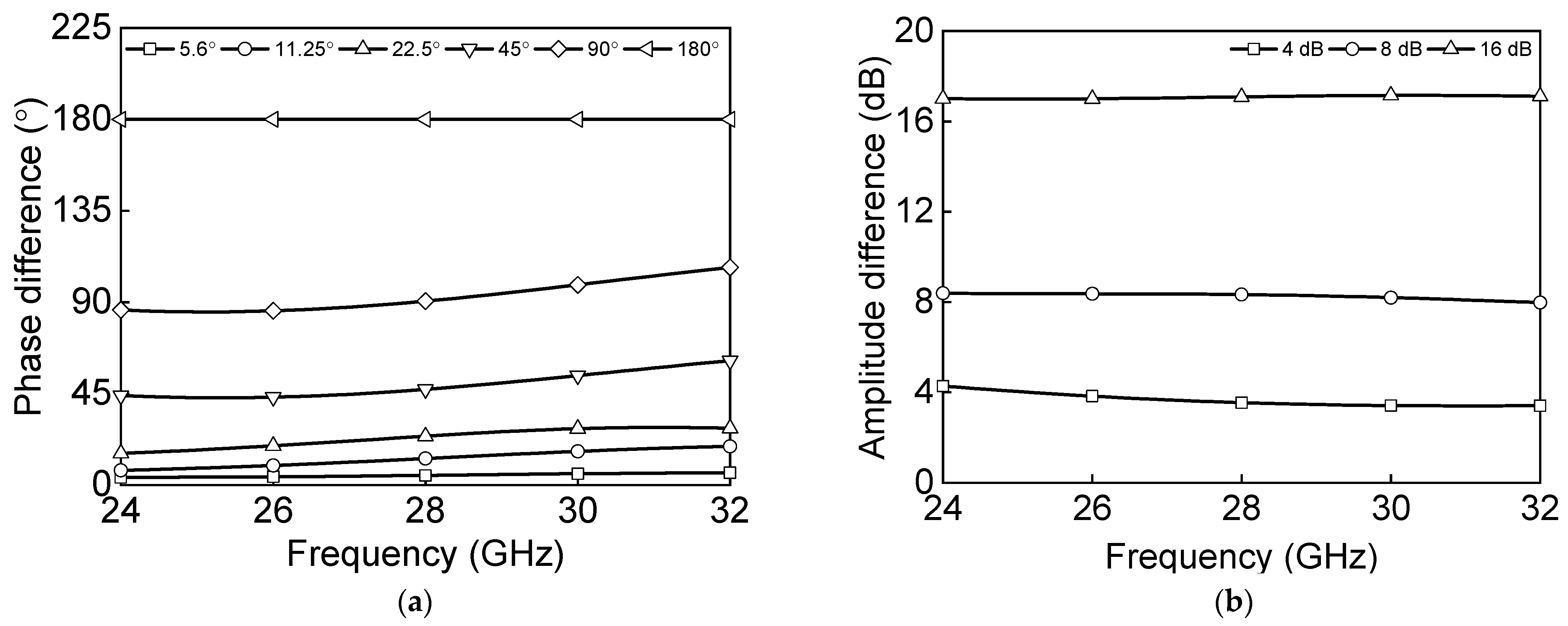
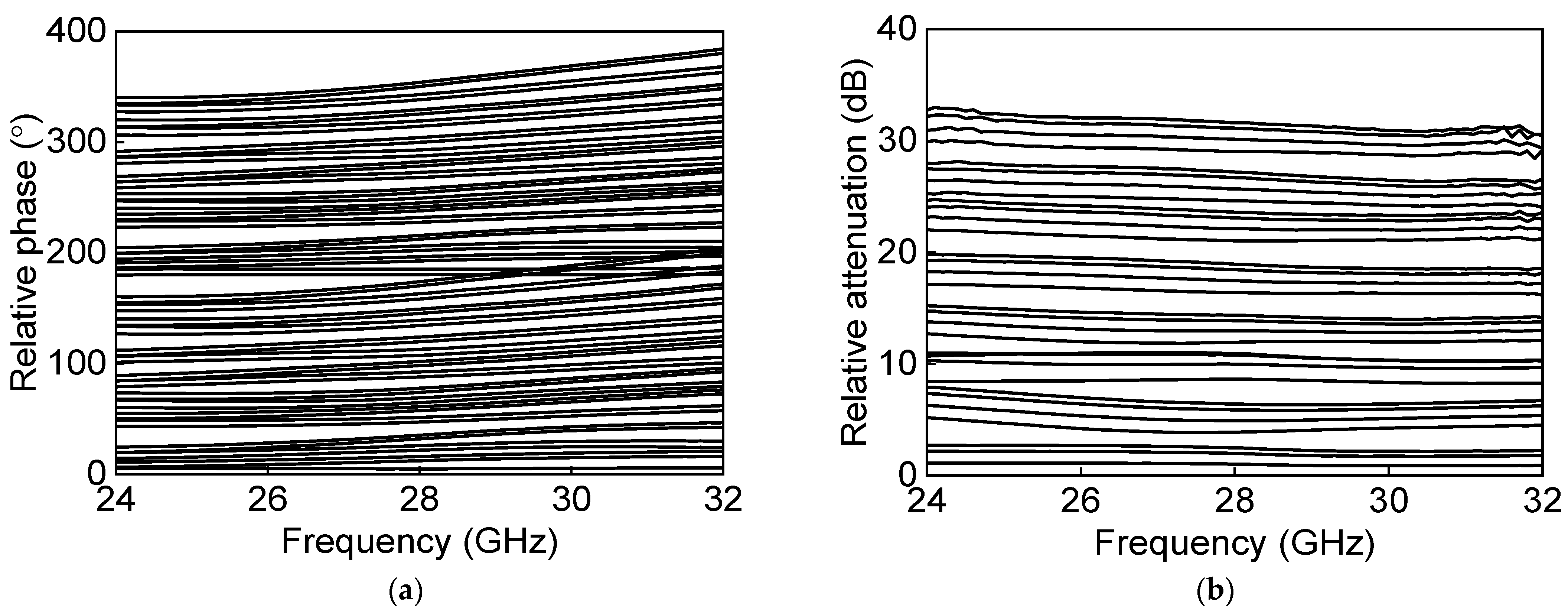
2.2. Differential Phase Shifters and Attenuators

The schematics of the proposed six-bit differential phase shifter and three-bit digital step attenuator, including the tuning bit, are shown in Figure 7. The phase shifter and attenuator are designed with a differential structure since it has advantages, such as improved linearity and reduced coupling between the signals at different ports. The phase shifter and attenuator circuits are distributed in a single block to make the compact chip size. The phase shifter and attenuator bits are cascaded in such an order to obtain better input and output matching and lower insertion loss.
The switched filter phase shifters are attractive for mm-wave design due to their high linearity and lack of DC power consumption. In addition, it can be implemented with a compact size and low insertion loss because it consists of lumped components, including NMOS transistor switches [12]. The six-bit differential phase shifter is designed with switched filter phase shifter structures. The 11.25° and 22.5° phase shifters are designed using a single inductor and bypass switch. When the series switch (T3 or T8) is on, the signal passes through the reference state. In the phase-shifting state, the switch (T3 or T8) is off and the signal passes through the series inductor (L1 or L4) with phase shifting of 11.25° and 22.5°, respectively. The 45° and 90° phase shifters are based on the switched-LC network using differential NMOS switches. In the phase-shifting state, T5_1 or T7_1 is off and T5_2 or T7_2 is on, making the π- network LPF. The signal is delayed when passing through the π- network LPF, making phase shifts of 45° and 90°, respectively. In the reference state, T5_1 or T7_1 is on and T5_2 or T7_2 is off, respectively. The inductors, L2_2 and L3_2, are adjusted to resonate with parasitic capacitance formed when transistors, T5_2 and T7_2, are off respectively. The design of the 180° phase shifter employs a minimalistic approach, relying solely on the cross-connected switch type to achieve the desired phase shift without the need for extra components, such as inductors or capacitors, resulting in a compact chip size. To achieve a tuning bit of 5.625°, a simple configuration consisting of a shunt NMOS transistor switch and a capacitor (C1) is used. To reduce the chip size, vertically stacked spiral inductors are used. All the inductors, MIM capacitors, and interconnection lines were designed using electromagnetic simulation.
The attenuator is used in calibrating amplitude error as well as sidelobe level reduction in the radiation pattern of an antenna. For zero DC power consumption, the attenuator is designed in a passive type, which is beneficial to be used in a large-scale phased array antenna system. Various topologies are available for the design of attenuators, including the switched path type, the distributed type, and the switched Pi/T-type attenuator [13]. The switched Pi/T-type attenuator is chosen based on its small size and low insertion loss. This type of attenuator is designed to be compact and efficient, using only three resistors and NMOS transistor switches to achieve the desired attenuation. The switched T-type attenuator is determined by Equations 1 and 2 where Z0 is the transmission line characteristic impedance and AdB is the desired attenuation in the dB scale.
R 1   = Z 0 10 A dB 20 1 10 A dB 20 + 1
R 2 = 2 Z 0 10 A dB 20 10 A dB 20 1
The differential 8 dB and 16 dB attenuators are designed using a switched T-type structure. The differential 4 dB attenuator and 1 dB attenuator are implemented with the shunt resistors, R2 and R3, and series switch transistors, T4 and T6, to reduce the chip size and loss. The attenuation state of 1 dB is used as a tuning bit to correct the amplitude error. Figure 8a shows the simulated phase difference of the main phase shift states of the six-bit phase shifter. Figure 8b shows the amplitude difference for each state of the three-bit attenuator.

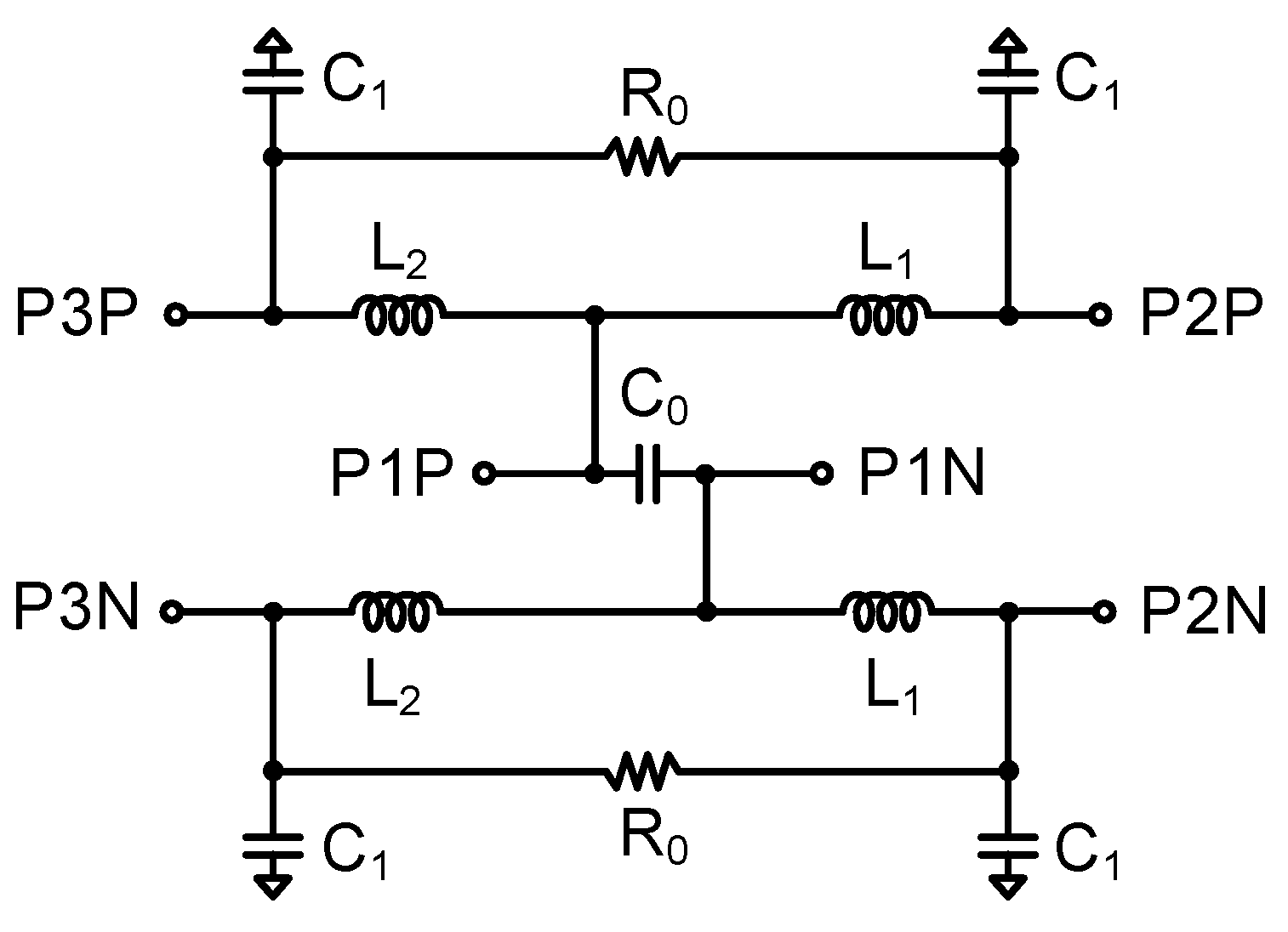
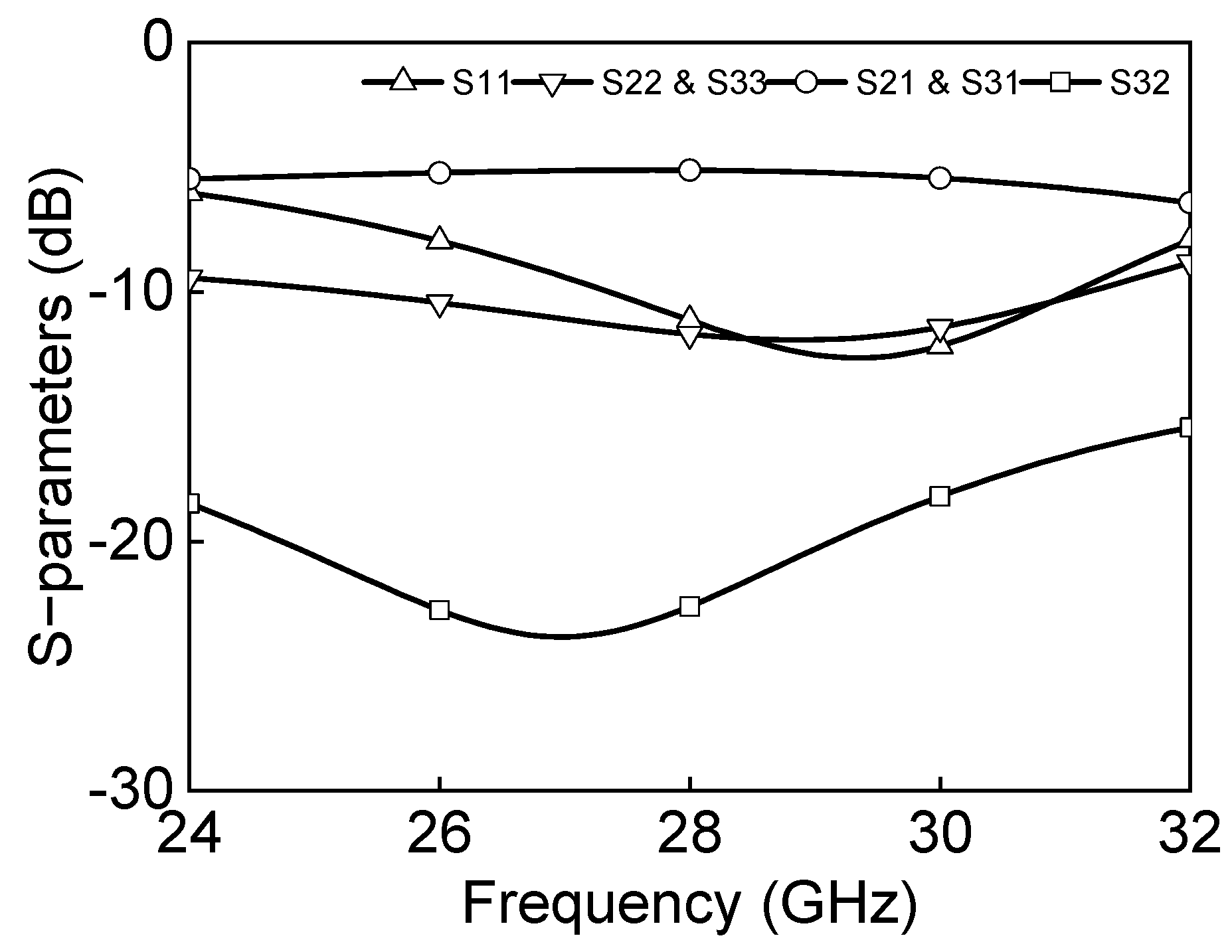
2.3. Differential Two-Way Power Divider
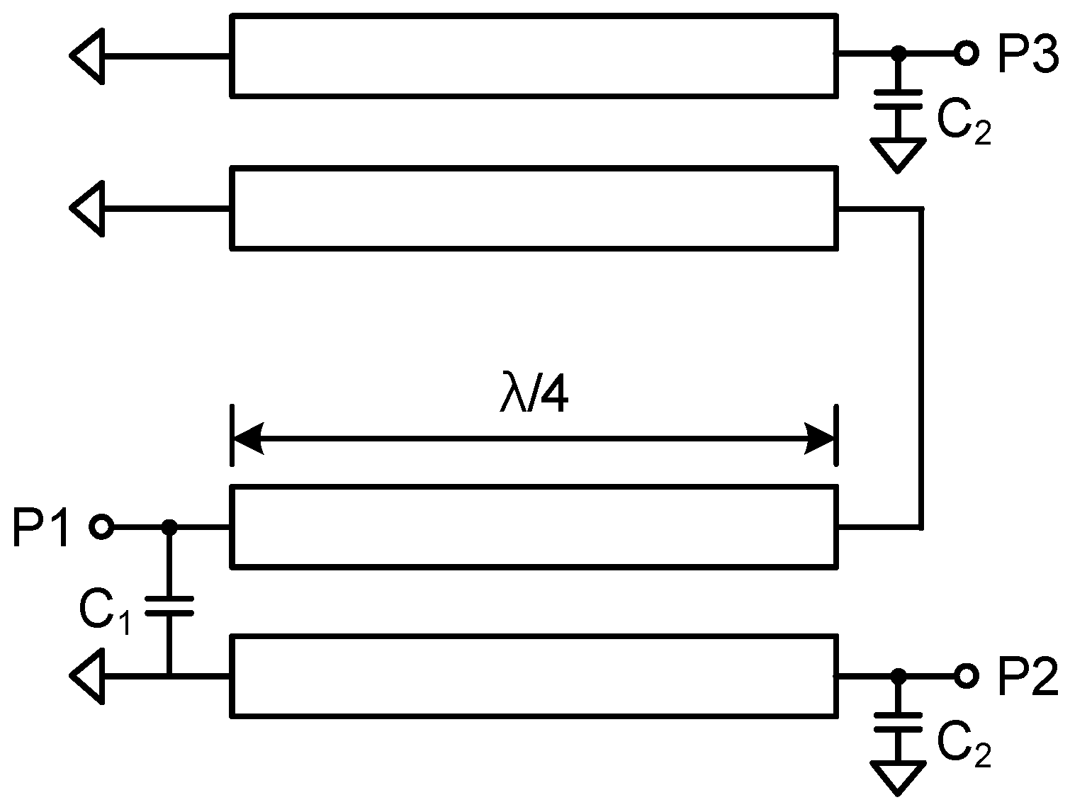
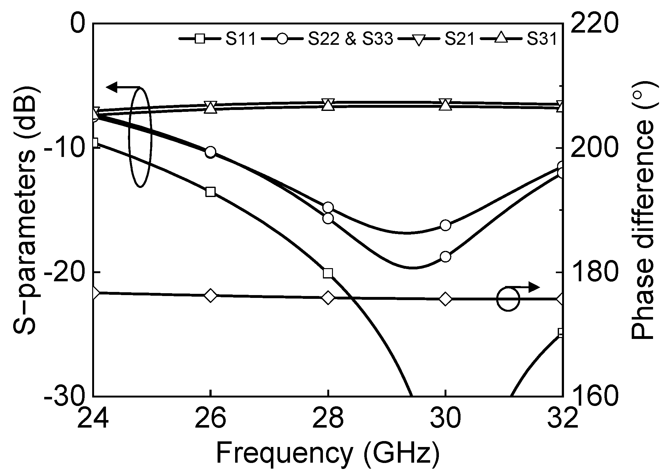
A power divider is implemented in the BFIC to split or combine the multiple channels transmit/receive signals. The two-way power divider is designed with differential structures, which is robust to parasitic inductances to the ground paths. The chip size is reduced using an artificial transmission line instead of the quarter-wavelength transmission line used in a conventional two-way power divider [14]. The schematic of the differential two-way power divider is shown in Figure 9. All capacitors in this circuit used metal-insulator-metal (MIM) capacitors.
L = Z 0 sin ϕ 4 π f ,   C = tan ϕ 2 2 π fZ 0
The inductance and capacitance in a differential two-way power divider are determined by Equation (3) where Z0 is the transmission line characteristic impedance and ϕ is the phase of the transmission line. Figure 10 shows the simulated insertion losses, return losses, and isolation. The insertion losses are −5.1 dB, and input/output return losses are under 10 dB at 27–29.5 GHz. The isolation between P2P and P2N and P3P and P3N is under 20 dB at 25–29.5 GHz.

2.4. Marchand Balun

The Marchand balun is implemented in transforming single-ended and differential signals. The Marchand balun is attractive due to its wideband performance, employing quarter wavelength coupled line sections. Figure 11 shows the schematic of the Marchand balun. The quarter-wavelength transmission lines are implemented as a vertically coupled structure, and the shunt capacitor helps compensate for impedance matching. Figure 12 shows the simulated insertion loss, return losses, and phase differences between differential output paths. The insertion losses of P1 to P2 and P1 to P3 are −6.3 dB and −6.7 dB at 27–29.5 GHz, respectively. The simulated return losses at each port are under 10 dB at 26–32 GHz, and the simulated phase difference is 176° at 26–32 GHz.

2.5. Differential SPDT Switch

A fully differential SPDT switch is designed to have high-power-handling capabilities for both the Tx and Rx paths and to have parasitic inductance robust performance as the CMOS switch structure has high insertion loss and low-power characteristics in high frequency. The body-floating technology is widely used in the CMOS switch to reduce insertion loss and improve power characteristics [15]. The body-floating technology can prevent leakage signals through the substrate and improve the insertion loss by adding a high-value resistor in the transistor body. Figure 13 shows the schematic of the proposed differential SPDT switch. The reflective SPDT switch is based on a series-shunt configuration for added isolation. The series transistors, T2 and T4, perform the main switching function, and the shunt transistors, T1 and T3, increase the isolation of the switch. In the design of SPDT switches, the gate terminals are biased through a large resistor to reduce the fluctuation in the VGD and VGS of the transistors due to the voltage swings at the drain and source terminals. Figure 14 shows the simulation results of the differential SPDT switch at output1 ON and output2 OFF states. The insertion loss of the differential SPDT switch is −2.7 dB, the return losses are under 10 dB, and the isolation is under 40 dB at 24–32 GHz.

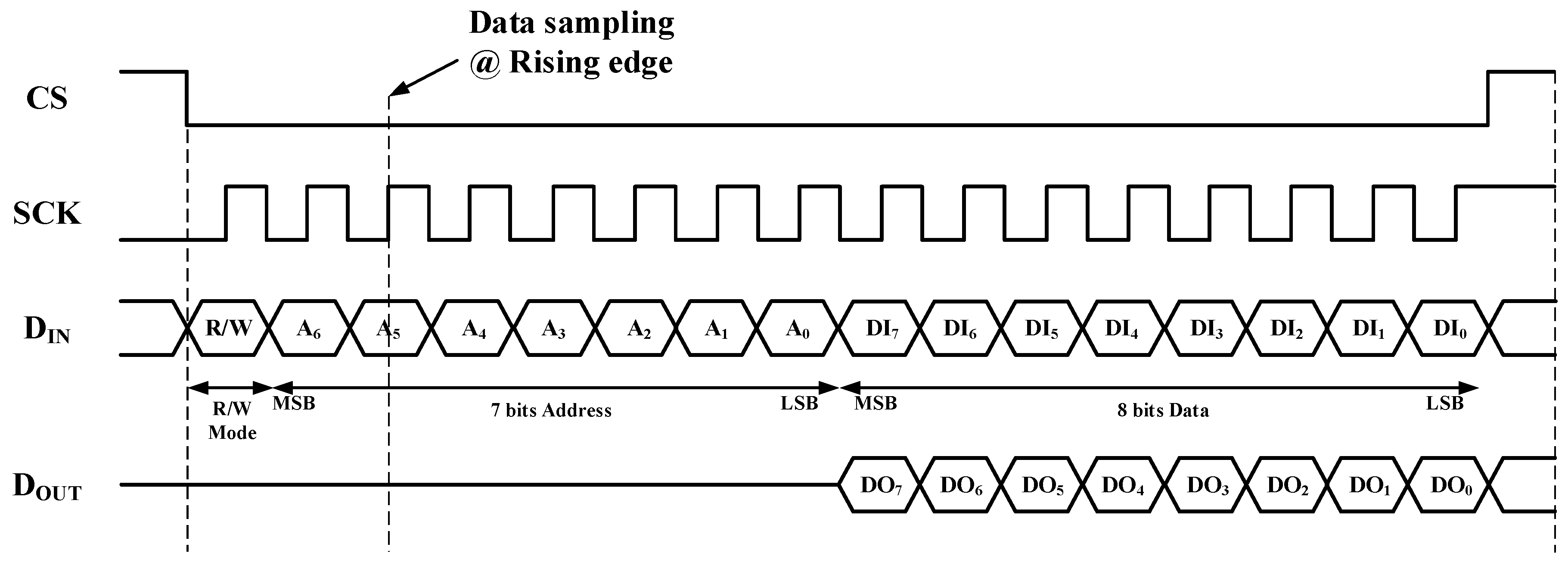
2.6. Serial Peripheral Interface

The gain and phase control for each channel is digitally controlled by the SPI. The timing diagram of the 16-bit SPI is shown in Figure 15. The SPI configuration utilized SPI mode 0 with a CPOL (clock polarity) of 0 and a CPHA (clock phase) of 0 where the data is sampled on the clock’s rising edge and shifted on the falling edge. The SPI protocol for the BFIC involves a 16-bit register where the first bit represents the read/write mode, seven bits represent the address, and the subsequent eight bits represent the data. When executing a write operation, the first bit of the address byte is set as ‘0’. The desired seven-bit address is assigned to the address field, and the eight-bit data field is filled with the required control information for the phase shifter, attenuator, and bias operation. To perform the read operation, the first bit of the address byte is set as ‘0’. The SPI interface supports a maximum operating speed of 20 MHz. The SPI design has been synthesized using Verilog code. The layout of the synthesized SPI block is shown in Figure 16. The size of the synthesized SPI block is 0.30 × 0.44 mm2.

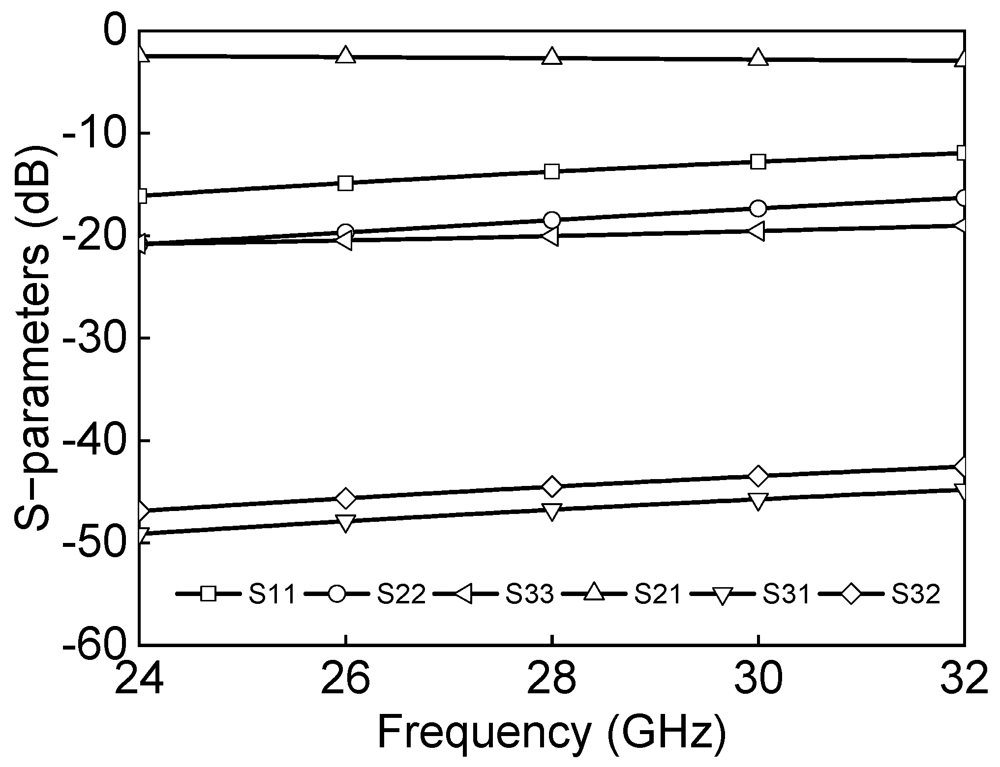
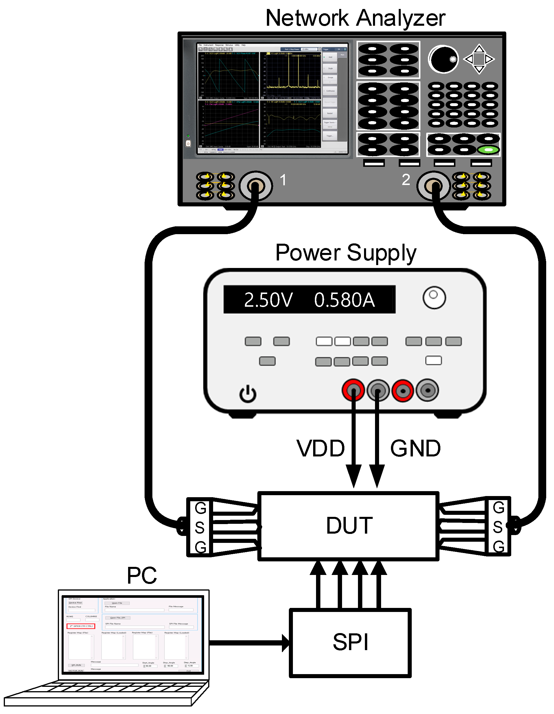
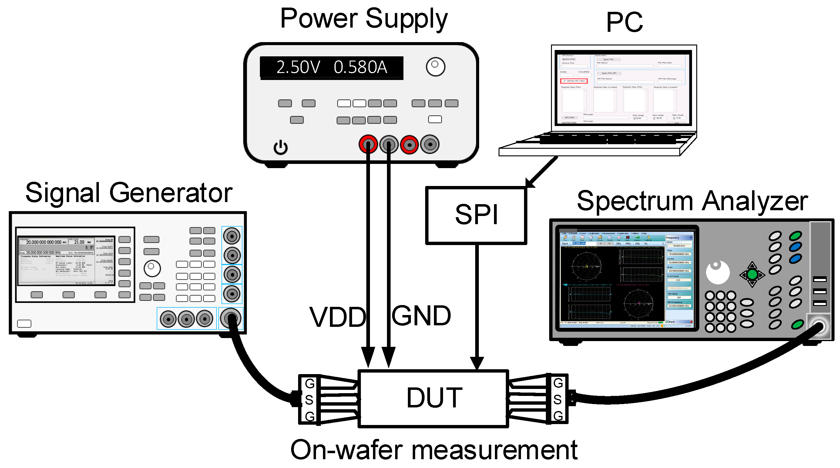
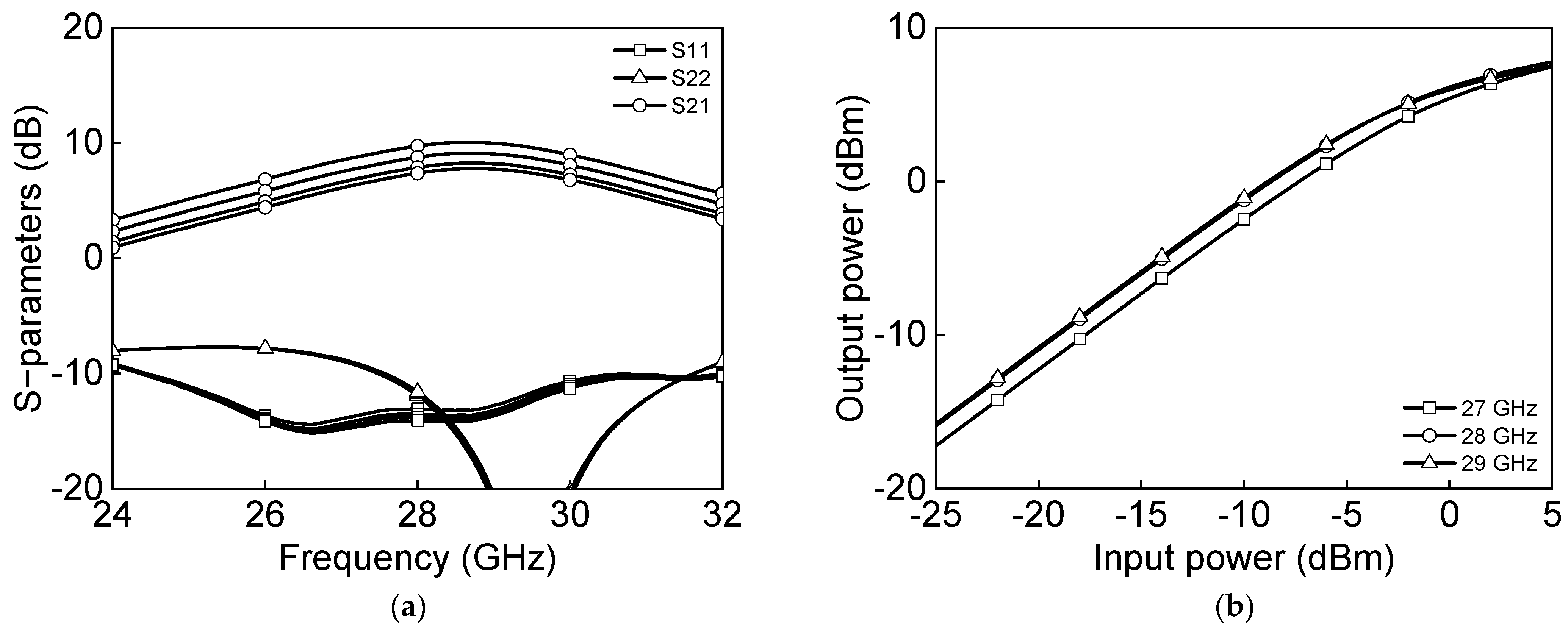
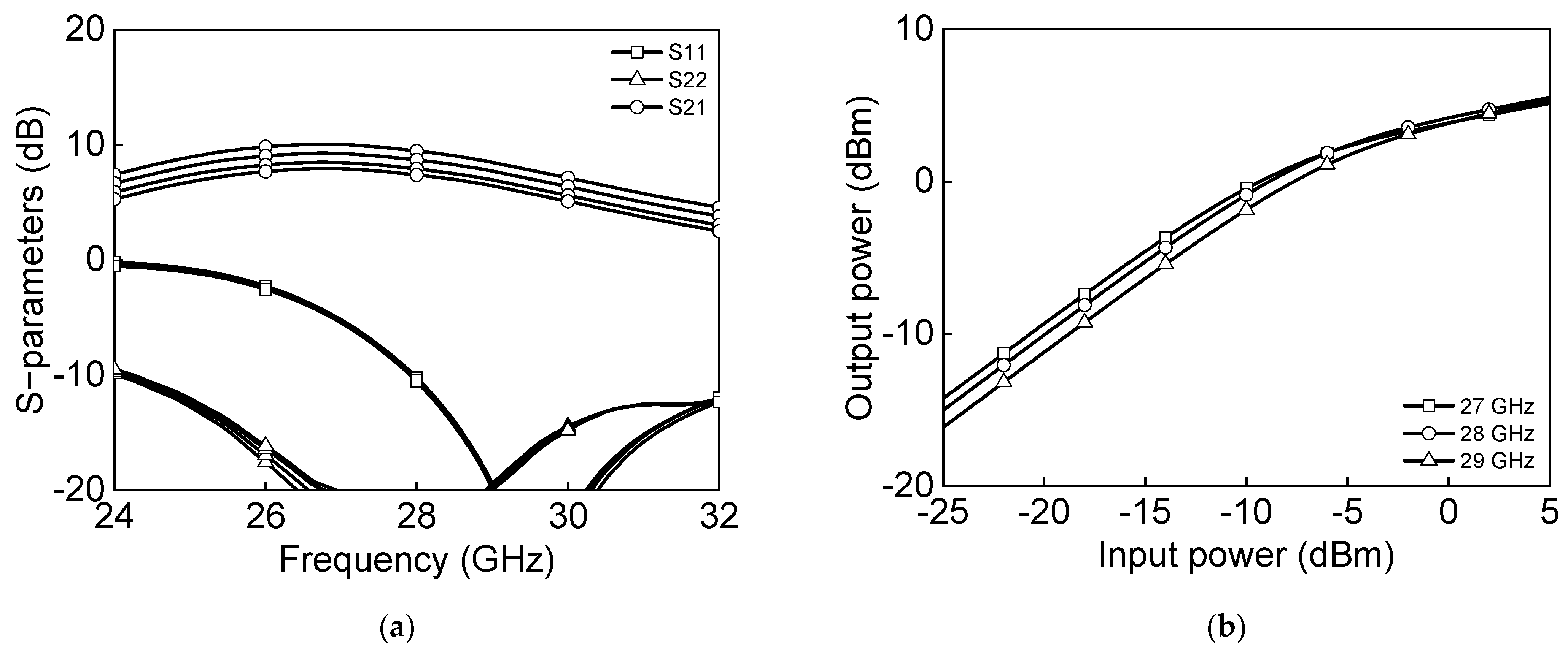
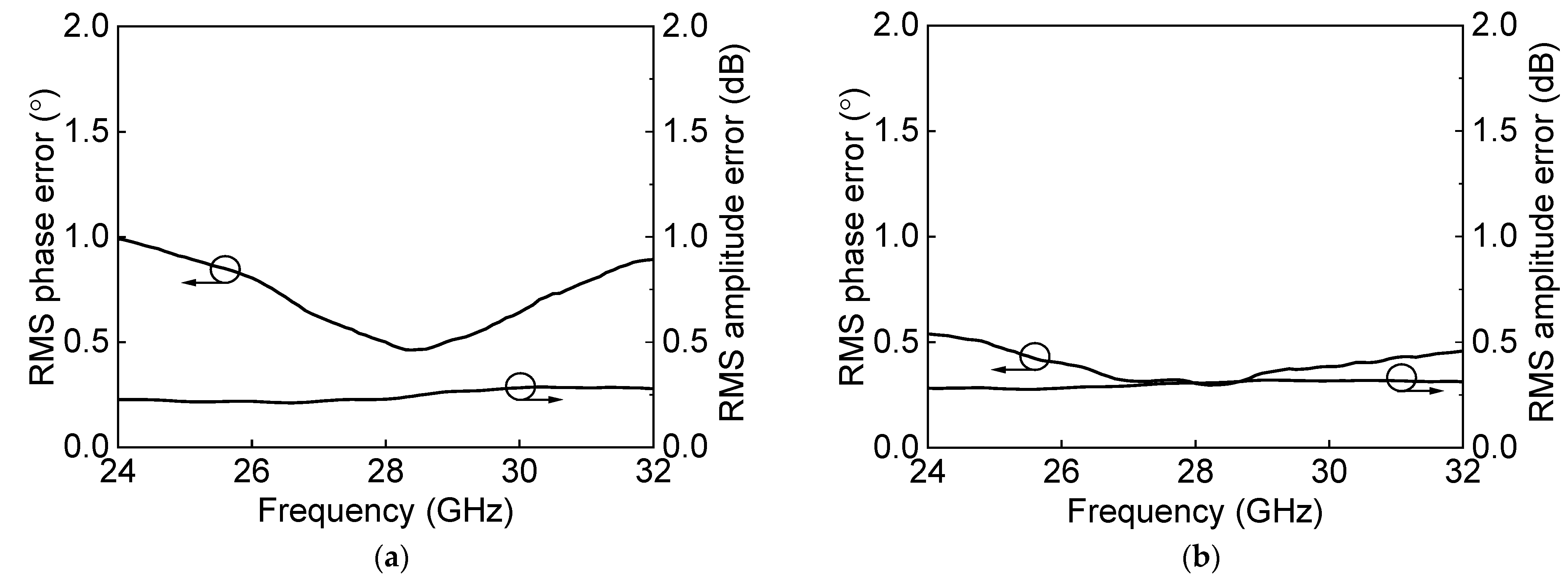
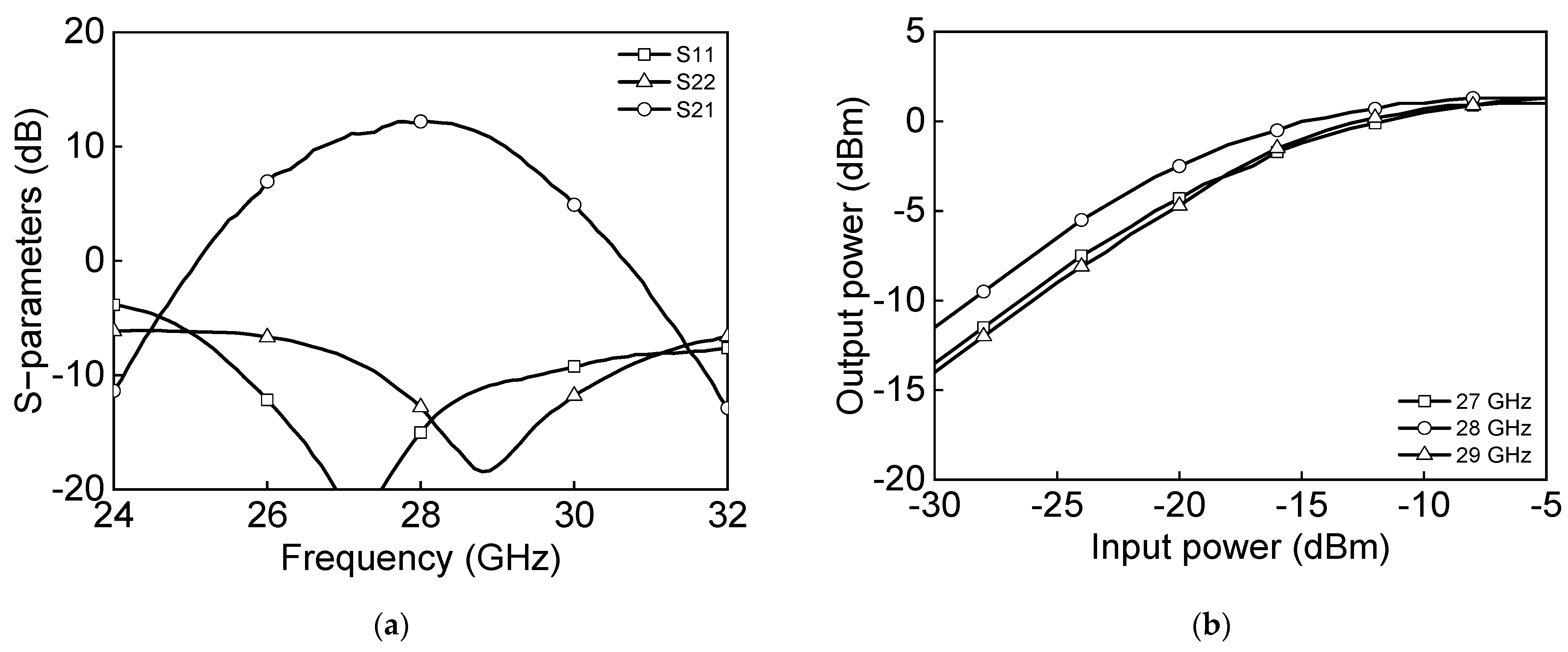
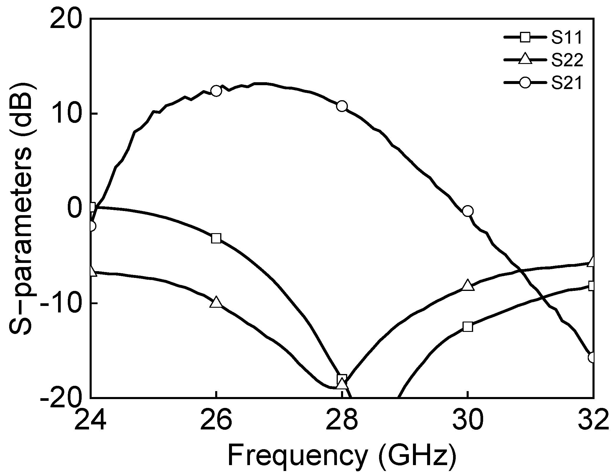
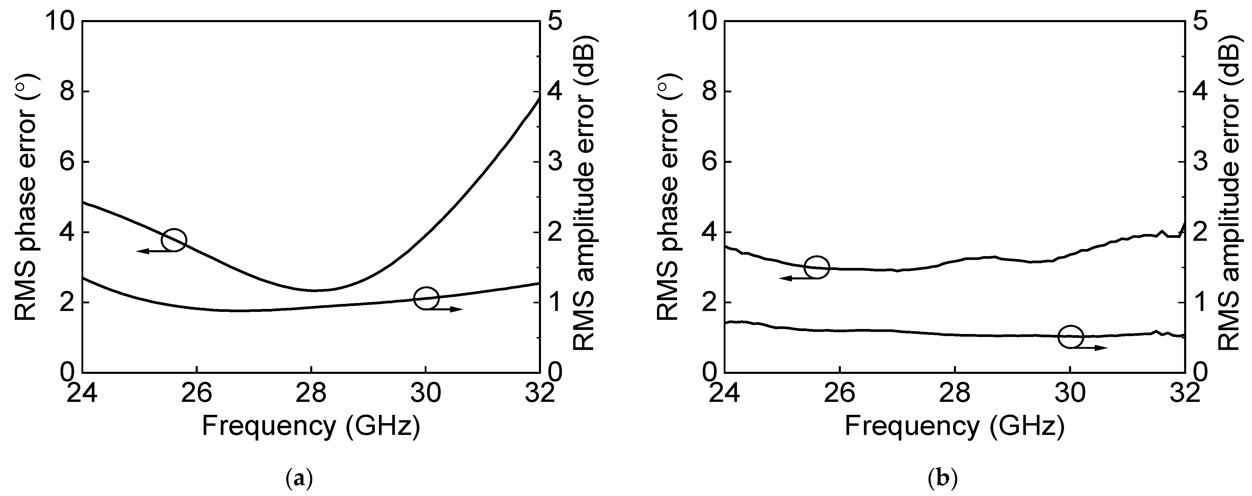
3. Measurement Results

The microphotograph of the fabricated 28 GHz eight-channel multimode BFIC fabricated in a commercial 65 nm CMOS technology is shown in Figure 17. The total area of the BFIC is 3.0 × 3.5 mm2, including pads. The DC current consumption of a 28 GHz eight-channel CMOS BFIC is 580 mA at 2.5 V supply voltage. The BFIC operates at a nominal voltage of 1.0 V and incorporates thin oxide technology. The measurements of the eight-channel BFIC are carried out with on-chip probing.
Figure 18 shows the on-wafer S-parameter measurement of the 28 GHz CMOS BFIC using a network analyzer. The short, open, load, and thru (SOLT) calibration was performed with the on-wafer probe station. The power characteristics are measured with the signal source and the spectrum analyzer. Figure 19 shows the on-wafer power characteristic measurement setup using the spectrum analyzer. This measurement method requires calibration from the measurement equipment port to the RF probe tip, including RF cables.
Figure 20 shows the microphotograph of the fabricated 28 GHz differential two-stage bi-directional amplifier. The use of the transformer-coupled structure makes the compact chip size. The chip size of the differential two-stage bi-directional amplifier is 0.44 × 0.28 mm2 without pads. Figure 21a shows the measured S-parameter in the Tx mode of the bi-directional amplifier. The measured Tx mode gain is around 9 dB, and return losses are under 10 dB at 27.0–29.5 GHz. The gain control of 3 dB is achieved with an attenuation step of 1 dB. Figure 21b shows the power characteristics in the Tx mode of the bi-directional amplifier. The measured Tx mode outputs, P1dB and PSAT, are 3.1 dBm and 7.8 dBm at 28 GHz, respectively. Figure 22a shows the measured S-parameter in the Rx mode of the bi-directional amplifier. The measured Rx mode gain is around 9 dB, and return losses are under 10 dB at 27.0–29.5 GHz. Due to the additional parasitic elements, the measured Rx mode gain operating frequency is slightly downshifted. Figure 22b shows the power characteristics in the Rx mode of the bi-directional amplifier. The measured Rx mode outputs, P1dB and PSAT, are −0.1 dBm and 5.5 dBm at 28 GHz, respectively. Figure 23a shows the RMS phase error and RMS amplitude error in the Tx mode of the differential two-stage bi-directional amplifier with attenuation control of 3 dB with an attenuation step of 1 dB. The RMS phase error is <0.5° at 27.0–29.5 GHz, and the RMS amplitude error is <0.2 dB at 27.0–29.5 GHz. Figure 23b shows the RMS phase error and RMS amplitude error in the Rx mode of the differential two-stage bi-directional amplifier with attenuation control of 0 dB to 3 dB. The RMS phase error is <0.3° at 27.0–29.5 GHz, and the RMS amplitude error is <0.3 dB at 27.0–29.5 GHz.
Figure 24a shows the measured S-parameter results in the Tx mode of the eight-channel BFIC. The measured Tx mode gain is around 11 dB, and return losses are under 10 dB at 27.0–29.5 GHz. Figure 24b shows the measured power characteristics in the Tx mode. The measured Tx mode outputs, P1dB and PSAT, are −2.5 dBm and 1.3 dBm at 28 GHz, respectively. Figure 25 shows the measured S-parameter results in the Rx mode of the eight-channel BFIC. The measured Rx mode gain is around 9 dB, and return losses are under 10 dB at 27.0–29.5 GHz. The operating frequency of the measured Rx mode gain is slightly downshifted due to the presence of additional parasitic elements. Figure 26a shows the measured relative phase characteristics in all the phase states. A phase variation range of 0° to 354° with a phase resolution of 5.625° is achieved. Figure 26b shows the measured attenuation characteristics in all the attenuation states. The attenuation range of 31 dB, including the gain control bits with an attenuation resolution of 1 dB, is achieved. To quantitively check the phase-shifting performance of the BFIC, the RMS phase and amplitude errors in all the phase shift states are presented. Figure 27a shows the measured RMS phase error and amplitude error when varying the phase states. The measured RMS phase error is <3°, and the RMS amplitude error is <2 dB at 27.0–29.5 GHz. Figure 27b shows the measured RMS phase error of <3.2° and the RMS attenuation error of <1 dB at 27.0–29.5 GHz when varying the attenuation states.
Table 1 summarizes the performance of this work and compares it with previously published 28 GHz beamforming ICs. The 28 GHz eight-channel multimode BFIC is designed with a differential structure to reduce interference from adjacent channels. The differential structure also allows common-mode rejection and less coupled signal at each port for multi-channel. The proposed BFIC has comparable RMS phase and amplitude error than the same RF phase-shifting architecture. The proposed BFIC allows for multimode operation based on the number of antenna requirements. The single BFIC is capable of operating in 8Tx and 8Rx modes separately as well as in a combined 8Tx8Rx TDD mode. Furthermore, it is capable of operating in four-channel mode, allowing the independent operation of 4Tx and 4Rx within a single BFIC.

4. Conclusions

This paper presents a multimode 28 GHz fully differential eight-channel BFIC in 65 nm CMOS technology for phased array transceivers. The bi-directional amplifier is implemented with a transformer coupled structure for compactness and low insertion loss. The cross connected quad switch type 180° phase bit and a differential two-way power divider using artificial transmission lines make the design compact and lower power consumption. The chip size is 3.0 × 3.5 mm2, including pads. The BFIC is capable of operating in multiple modes, enabling it to operate in the 8Tx and 8Rx modes separately, the 8Tx8Rx TDD mode, and also in four-channel mode 4Tx and 4Rx independently. The proposed 28 GHz fully differential eight-channel BFIC with a multimode operation can be implemented in mm-wave base stations and mobile devices.

Author Contributions

Conceptualization, A.B., J.P. and J.-G.K.; methodology, A.B., J.P. and J.-G.K.; investigation, A.B., J.P. and J.-G.K.; writing—original draft preparation, A.B., J.P. and J.-G.K.; writing—review and editing, A.B. and J.-G.K.; supervision, D.B. and J.-G.K.; project administration, D.B. and J.-G.K.; funding acquisition, J.-G.K. All authors have read and agreed to the published version of the manuscript.

Funding

This work was supported by the Institute of Information & Communications Technology Planning & Evaluation (IITP) grant funded by the Korea government (MSIT) (No. 2018-0-01663, Development of Communication Sensing Converged B5G Millimeter Wave System) and has been conducted by the Research Grant of Kwangwoon University in 2022 in part.

Institutional Review Board Statement

Not applicable.

Informed Consent Statement

Not applicable.

Data Availability Statement

The data can be obtained from the authors on request.

Conflicts of Interest

The authors declare no conflict of interest.

References

  1. Ahmed, N.; Kibaroglu, K.; Sayginer, M.; Rebeiz, G.M. An In-Situ Self-Test and Self-Calibration Technique Utilizing Antenna Mutual Coupling for 5G Multi-Beam TRX Phased Arrays. In Proceedings of the 2019 IEEE MTT-S International Microwave Symposium (IMS), Boston, MA, USA, 2–7 June 2019; pp. 1229–1232. [Google Scholar]
  2. Kibaroglu, K.; Sayginer, M.; Phelps, T.; Rebeiz, G.M. A 64-Element 28-GHz Phased-Array Transceiver with 52-dBm EIRP and 8–12-Gb/s 5G Link at 300 Meters without Any Calibration. IEEE Trans. Microw. Theory Tech. 2022, 70, 1715–1724. [Google Scholar] [CrossRef]
  3. Park, J.; Baek, D.; Kim, J.-G. A 28 GHz 8-Channel Fully Differential Beamforming IC in 65 nm CMOS Process. In Proceedings of the 2019 49th European Microwave Conference (EuMC), Paris, France, 29 September–4 October 2019; pp. 476–479. [Google Scholar]
  4. Park, J.; Lee, S.; Chun, J.; Jeon, L.; Hong, S. A 28-GHz Four-Channel Beamforming Front-End IC with Dual-Vector Variable Gain Phase Shifters for 64-Element Phased Array Antenna Module. IEEE J. Solid-State Circuits 2023, 58, 1142–1159. [Google Scholar] [CrossRef]
  5. Shinjo, S.; Nakatani, K.; Kamioka, J.; Komaru, R.; Noto, H.; Nakamizo, H.; Yamaguchi, S.; Uchida, S.; Okazaki, A.; Yamanaka, K. A 28GHz-Band Highly Integrated GaAs RF Frontend Module for Massive MIMO in 5G. In Proceedings of the 2018 IEEE MTT-S International Microwave Workshop Series on 5G Hardware and System Technologies (IMWS-5G), Dublin, Ireland, 27–29 August 2018; pp. 1–3. [Google Scholar]
  6. Sadhu, B.; Tousi, Y.; Hallin, J.; Sahl, S.; Reynolds, S.K.; Renstrom, O.; Sjogren, K.; Haapalahti, O.; Mazor, N.; Bokinge, B.; et al. A 28-GHz 32-Element TRX Phased-Array IC with Concurrent Dual-Polarized Operation and Orthogonal Phase and Gain Control for 5G Communications. IEEE J. Solid-State Circuits 2017, 52, 3373–3391. [Google Scholar] [CrossRef]
  7. Huang, M.Y.; Chi, T.; Li, S.; Huang, T.Y.; Wang, H. A 24.5–43.5-GHz Ultra-Compact CMOS Receiver Front End with Calibration-Free Instantaneous Full-Band Image Rejection for Multiband 5G Massive MIMO. IEEE J. Solid-State Circuits 2020, 55, 1177–1186. [Google Scholar] [CrossRef]
  8. Dunworth, J.D.; Jin, S.; Keeler, R.; Kwack, J.; Murphy, J.; Chevalier, P.; Pekarik, J.; Lee, K.; Ryu, K.; Lee, J.; et al. A 28 GHz Bulk-CMOS Dual-Polarization Phased-Array Transceiver with 24 Channels for 5G User and Basestation Equipment. In Proceedings of the 2018 IEEE International Solid-State Circuits Conference (ISSCC), San Francisco, CA, USA, 11–15 February 2018; pp. 70–72. [Google Scholar]
  9. Chu, C.-Y.; Huang, C.-Y.; Chang, H.-S.; Hsieh, Y.-C.; Shih, C.-J.; Wang, Y.-H.; Chuang, H.-Y.; Wu, J.-S.; Horng, T.-S. A Fully-Integrated Ka-Band 4TX/4RX Phased-Array Transceiver IC in 65nm CMOS. In Proceedings of the 2016 IEEE International Symposium on Radio-Frequency Integration Technology (RFIT), Taipei, Taiwan, 12–14 December 2016; pp. 1–3. [Google Scholar]
  10. Kibaroglu, K.; Sayginer, M.; Rebeiz, G.M. A Low-Cost Scalable 32-Element 28-GHz Phased Array Transceiver for 5G Communication Links Based on a 2 × 2 Beamformer Flip-Chip Unit Cell. IEEE J. Solid-State Circuits 2018, 53, 1260–1274. [Google Scholar] [CrossRef]
  11. Li, Z.; Pang, J.; Kubozoe, R.; Luo, X.; Wu, R.; Wang, Y.; You, D.; Fadila, A.A.; Alvin, J.; Liu, B.; et al. A 28 GHz CMOS Differential Bi-Directional Amplifier for 5G NR. In Proceedings of the 2020 25th Asia and South Pacific Design Automation Conference (ASP-DAC), Beijing, China, 13–16 January 2020; pp. 5–6. [Google Scholar]
  12. Jung, M.; Min, B.-W. A Compact Ka-Band 4-bit Phase Shifter with Low Group Delay Deviation. IEEE Microw. Wirel. Compon. Lett. 2020, 30, 414–416. [Google Scholar] [CrossRef]
  13. Yuan, Y.; Mu, S.-X.; Guo, Y.-X. 6-Bit Step Attenuators for Phased-Array System with Temperature Compensation Technique. IEEE Microw. Wirel. Compon. Lett. 2018, 28, 690–692. [Google Scholar] [CrossRef]
  14. Janisz, K.; Wincza, K.; Gruszczynski, S. Differential Lumped-Element Wilkinson Power Divider for Use in MMIC Systems. In Proceedings of the 2017 Mediterranean Microwave Symposium, Ljubljana, Slovenia, 22–24 November 2017; pp. 1–3. [Google Scholar]
  15. Lee, W.; Hong, S. Small-Size Low-Loss 28-GHz Body-Floated CMOS DPDT Switch Using Shared Matching Network. IEEE Microw. Wirel. Compon. Lett. 2018, 28, 1113–1115. [Google Scholar] [CrossRef]
  16. Pang, J.; Wu, R.; Wang, Y.; Dome, M.; Kato, H.; Huang, H.; Narayanan, A.T.; Liu, H.; Liu, B.; Nakamura, T.; et al. A 28-GHz CMOS Phased-Array Transceiver Based on LO Phase-Shifting Architecture with Gain Invariant Phase Tuning for 5G New Radio. IEEE J. Solid-State Circuits 2019, 54, 1228–1242. [Google Scholar] [CrossRef]
  17. Kim, H.-T.; Park, B.-S.; Song, S.-S.; Moon, T.-S.; Kim, S.-H.; Chang, J.-M.; Ho, Y.-C. A 28-GHz CMOS direct conversion transceiver with packaged 2 × 4 antenna arrays for 5G cellular system. IEEE J. Solid-State Circuits 2018, 53, 1245–1259. [Google Scholar] [CrossRef]
Figure 1. Block diagram of 28 GHz eight-channel multimode beamforming IC.
Sensors 23 06124 g001
Figure 2. Simplified block diagram of multimode operation of 28 GHz eight-channel CMOS beamforming IC: (a) 8Tx mode, (b) 8Rx mode, (c) 8Tx8Rx TDD mode, and (d) 4Tx and 4Rx independent mode.
Sensors 23 06124 g002
Figure 3. Schematic of the transformer coupled differential two-stage bi-directional amplifier.
Sensors 23 06124 g003
Figure 4. Equivalent circuit diagram of the differential two-stage bi-directional amplifier: (a) Tx mode and (b) Rx mode.
Sensors 23 06124 g004
Figure 5. Simulated results of differential two−stage bi−directional amplifier in Tx−mode: (a) s−parameter (b) power characteristics.
Sensors 23 06124 g005
Figure 6. Simulated results of differential two−stage bi−directional amplifier in Rx−mode: (a) s−parameter and (b) power characteristics.
Sensors 23 06124 g006
Figure 7. Schematic of the six-bit phase shifter and the three-bit digital step attenuator with tuning bit.
Sensors 23 06124 g007
Figure 8. Simulated results: (a) phase difference of six-bit phase shifter and (b) amplitude difference of three-bit attenuator.
Sensors 23 06124 g008
Figure 9. Schematic of the differential two-way power divider.
Sensors 23 06124 g009
Figure 10. Simulation results of the differential two−way power divider.
Sensors 23 06124 g010
Figure 11. Schematic of the Marchand balun.
Sensors 23 06124 g011
Figure 12. Simulation results of the Marchand balun.
Sensors 23 06124 g012
Figure 13. Schematic of the differential SPDT switch.
Sensors 23 06124 g013
Figure 14. Simulation results of the differential SPDT switch.
Sensors 23 06124 g014
Figure 15. Timing diagram of the 16-bit SPI.
Sensors 23 06124 g015
Figure 16. Layout of the synthesized SPI block.
Sensors 23 06124 g016
Figure 17. Microphotograph of the proposed 28 GHz CMOS eight-channel multimode beamforming IC.
Sensors 23 06124 g017
Figure 18. Measurement setup of on-wafer S-parameter of 28 GHz CMOS beamforming IC.
Sensors 23 06124 g018
Figure 19. Measurement setup of on-wafer power characteristics of 28 GHz CMOS beamforming IC.
Sensors 23 06124 g019
Figure 20. Microphotograph of the proposed differential two-stage bi-directional amplifier.
Sensors 23 06124 g020
Figure 21. Measured Tx mode differential bi−directional amplifier: (a) S−parameters and (b) power characteristics.
Sensors 23 06124 g021
Figure 22. Measured Rx mode differential bi−directional amplifier: (a) S−parameters and (b) power characteristics.
Sensors 23 06124 g022
Figure 23. Measured RMS errors of the differential bi−directional amplifier with (a) Tx mode attenuation control and (b) Rx mode attenuation control.
Sensors 23 06124 g023
Figure 24. Measured Tx mode: (a) S−parameters and (b) power characteristics.
Sensors 23 06124 g024
Figure 25. Measured Rx mode S−parameters.
Sensors 23 06124 g025
Figure 26. Measured (a) phase characteristics and (b) attenuation characteristics.
Sensors 23 06124 g026
Figure 27. Measured RMS errors with (a) phase control and (b) attenuation control.
Sensors 23 06124 g027
Table 1. Summary of 28 GHz multimode beamforming IC for phased array transceiver.
Ref.This Work[4][16][17]
Tech (CMOS)65 nm65 nm65 nm28 nm
Freq. (GHz)27.0–29.526.5–3026.5–29.525.8–28
Number of channels8 TRx4TRx4 TRx8 TRx
Single-ended/DifferentialDifferentialDifferentialDifferentialSingle-ended
Tx/Rx Gain (dB) 11/918.6/14.89/11N/A
P1dB/PSAT (dBm) −2.5/1.313.3/-15.7/189.5/10.5
Phase shift step (o)6 bit/5.66 bit/5.62 + 3 + 10 bit/0.3 **3 bit/45
RMS amplitude error (dB)0.60.210.041
RMS phase error (o)3.21.40.37
Tx/Rx PDC of 1channel (mW)181/18173/-299/14885/50 *
Mode8Tx only
8Rx only
8Tx8Rx TDD
4Tx4Rx-
independent
4Tx only
4Rx only
4Tx4Rx-
independent
4Tx only
4Rx only
4Tx4Rx-
independent
8Tx only
8Rx only
8Tx8Rx TDD
Chip Size (mm2)10.50.92 ***127.3
* Estimated from the data. ** Step limited by phase error. *** One-Channel core size.
Disclaimer/Publisher’s Note: The statements, opinions and data contained in all publications are solely those of the individual author(s) and contributor(s) and not of MDPI and/or the editor(s). MDPI and/or the editor(s) disclaim responsibility for any injury to people or property resulting from any ideas, methods, instructions or products referred to in the content.

