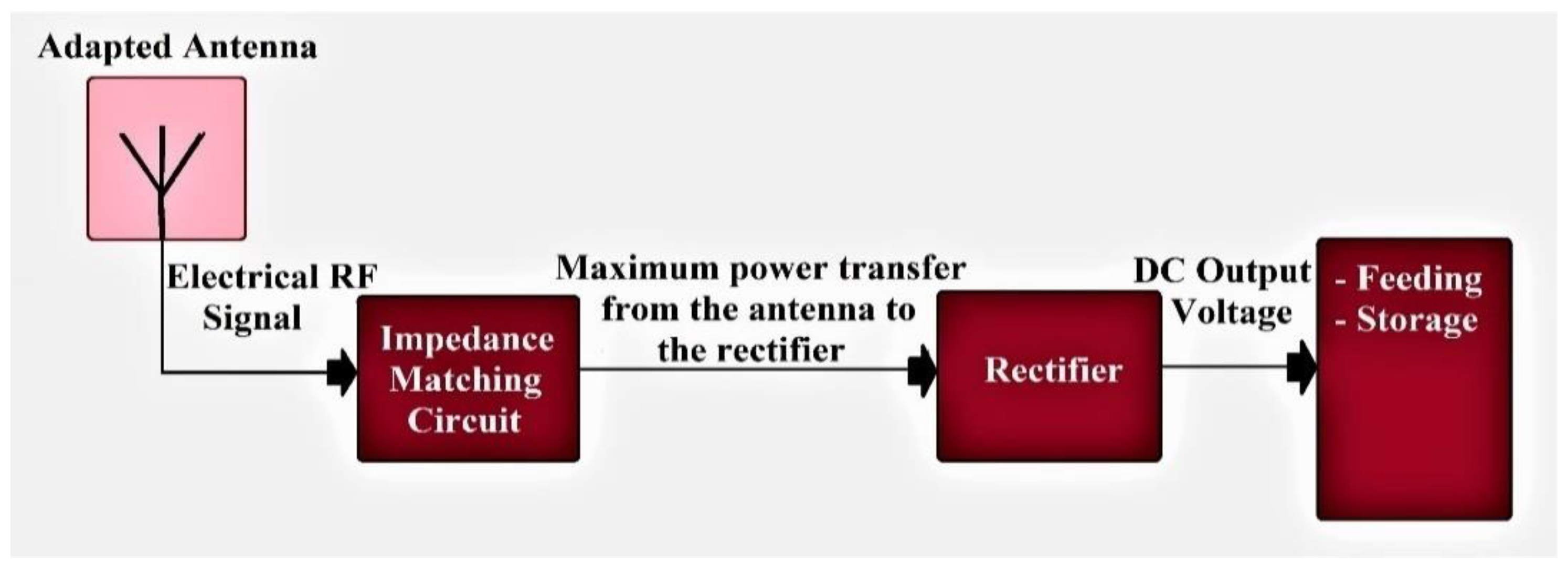
Figure 1.
RF Energy Harvesting system blocks.
Figure 1.
RF Energy Harvesting system blocks.
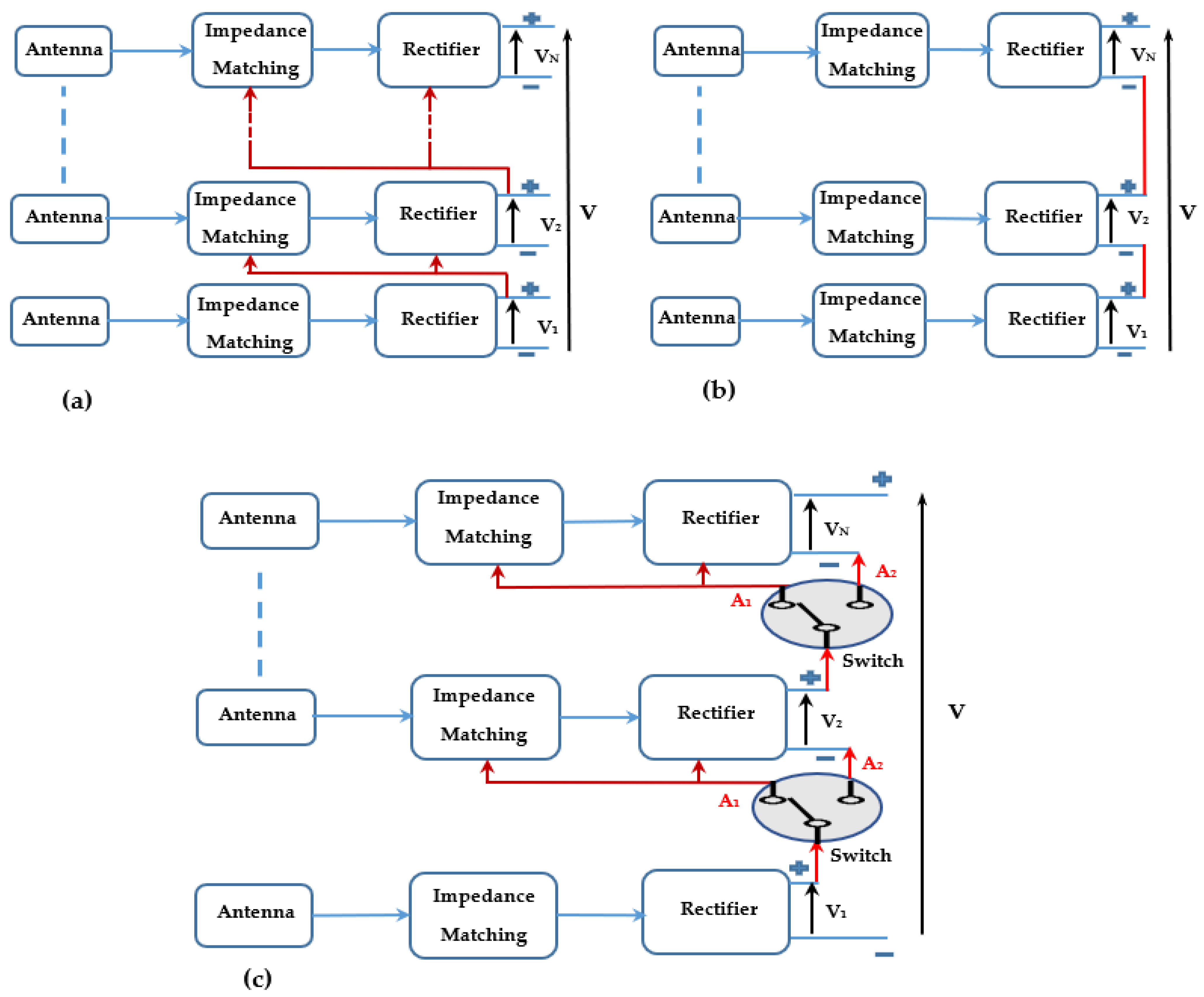
Figure 2.
Block diagram of (a) first architecture (RF-EH1), (b) second architecture (RF-EH2), and (c) the proposed system RF-EH. A1 and A2 are the two positions corresponding to first and second architectures.
Figure 2.
Block diagram of (a) first architecture (RF-EH1), (b) second architecture (RF-EH2), and (c) the proposed system RF-EH. A1 and A2 are the two positions corresponding to first and second architectures.
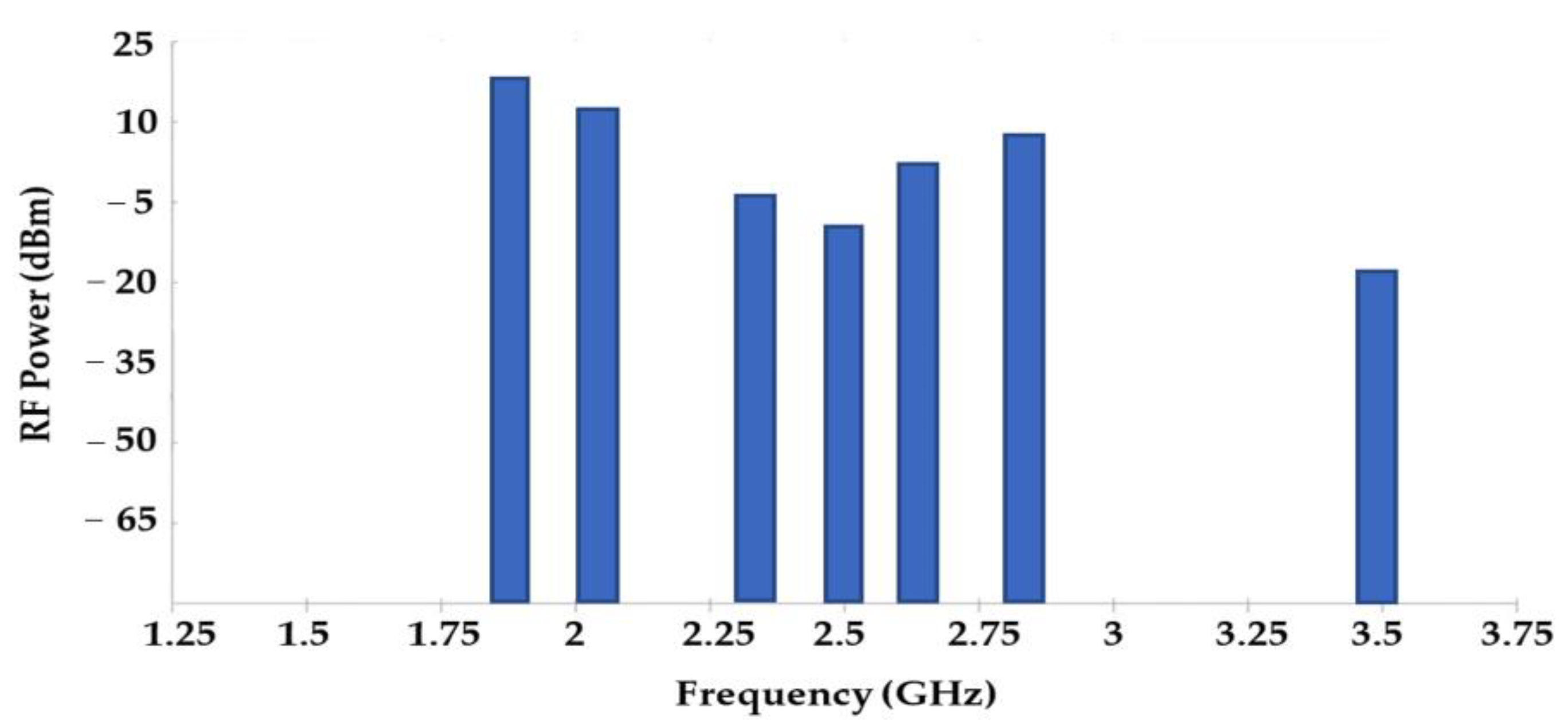
Figure 3.
Measured ambient RF power at 22 m from mobile communication base station.
Figure 3.
Measured ambient RF power at 22 m from mobile communication base station.
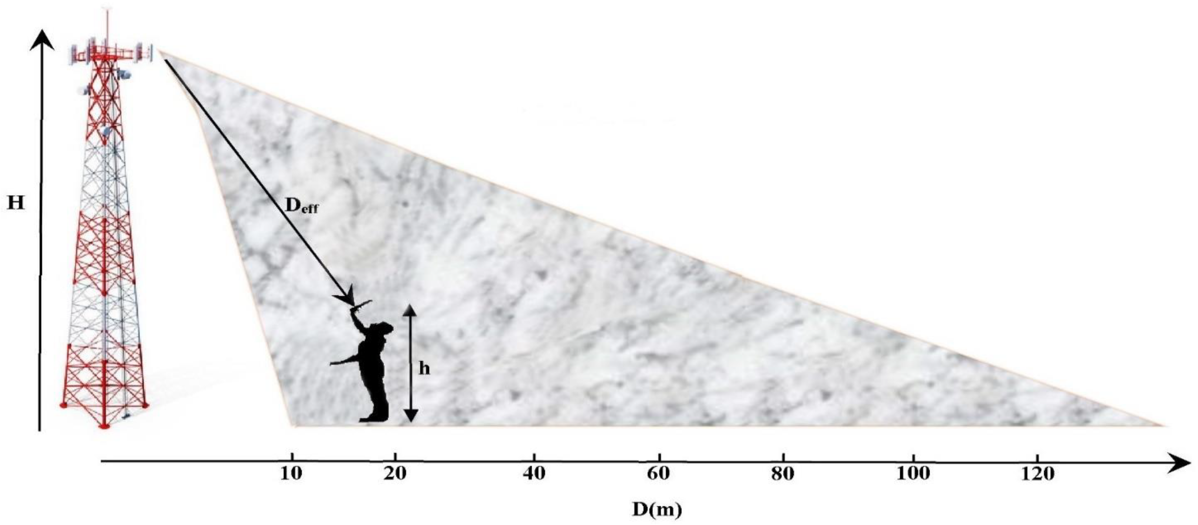
Figure 4.
Geometric parameters of measurement field. Deff: Effective distance.
Figure 4.
Geometric parameters of measurement field. Deff: Effective distance.
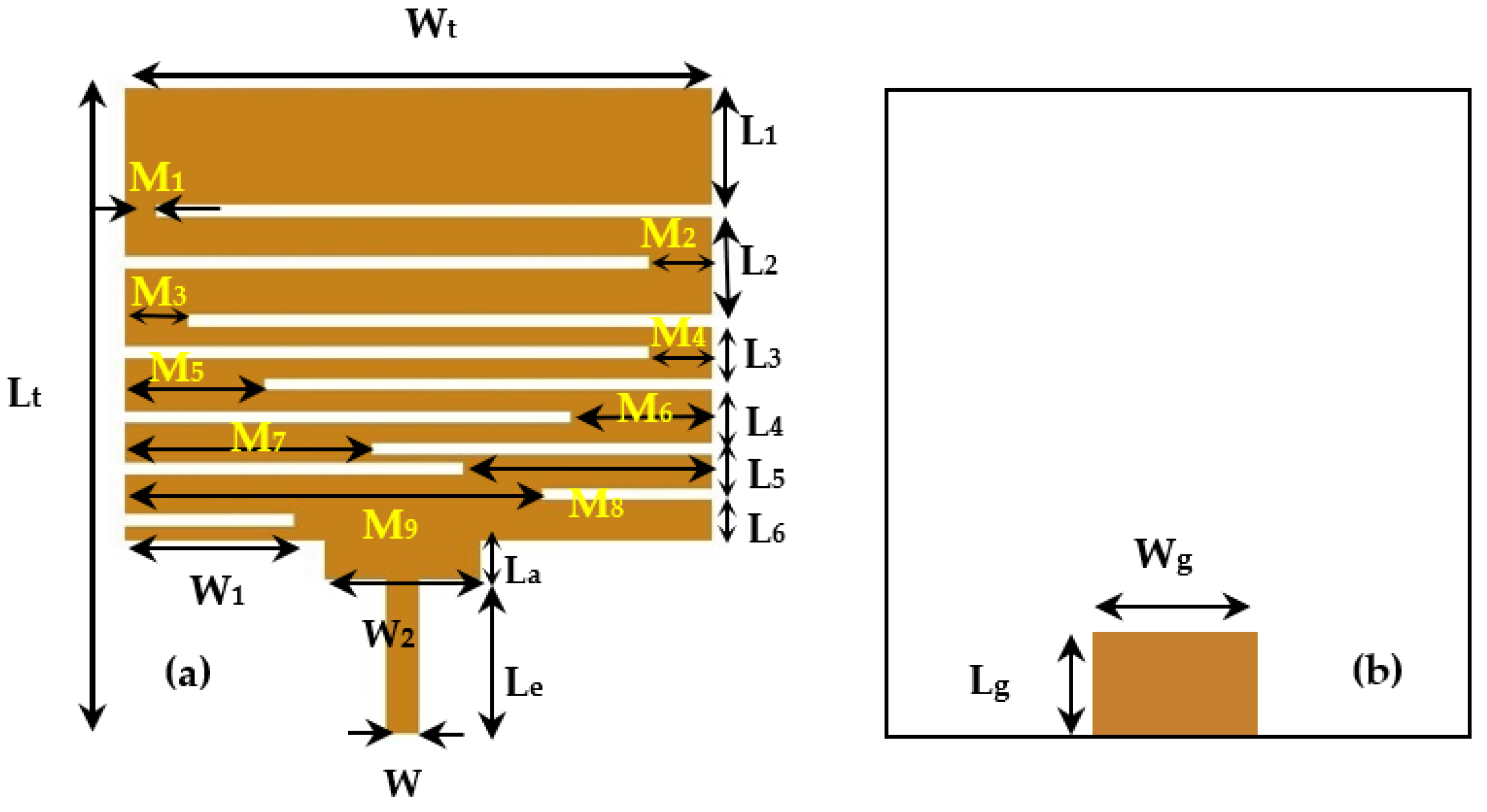
Figure 5.
Proposed antenna structure, (a) Top side, (b) Bottom side.
Figure 5.
Proposed antenna structure, (a) Top side, (b) Bottom side.
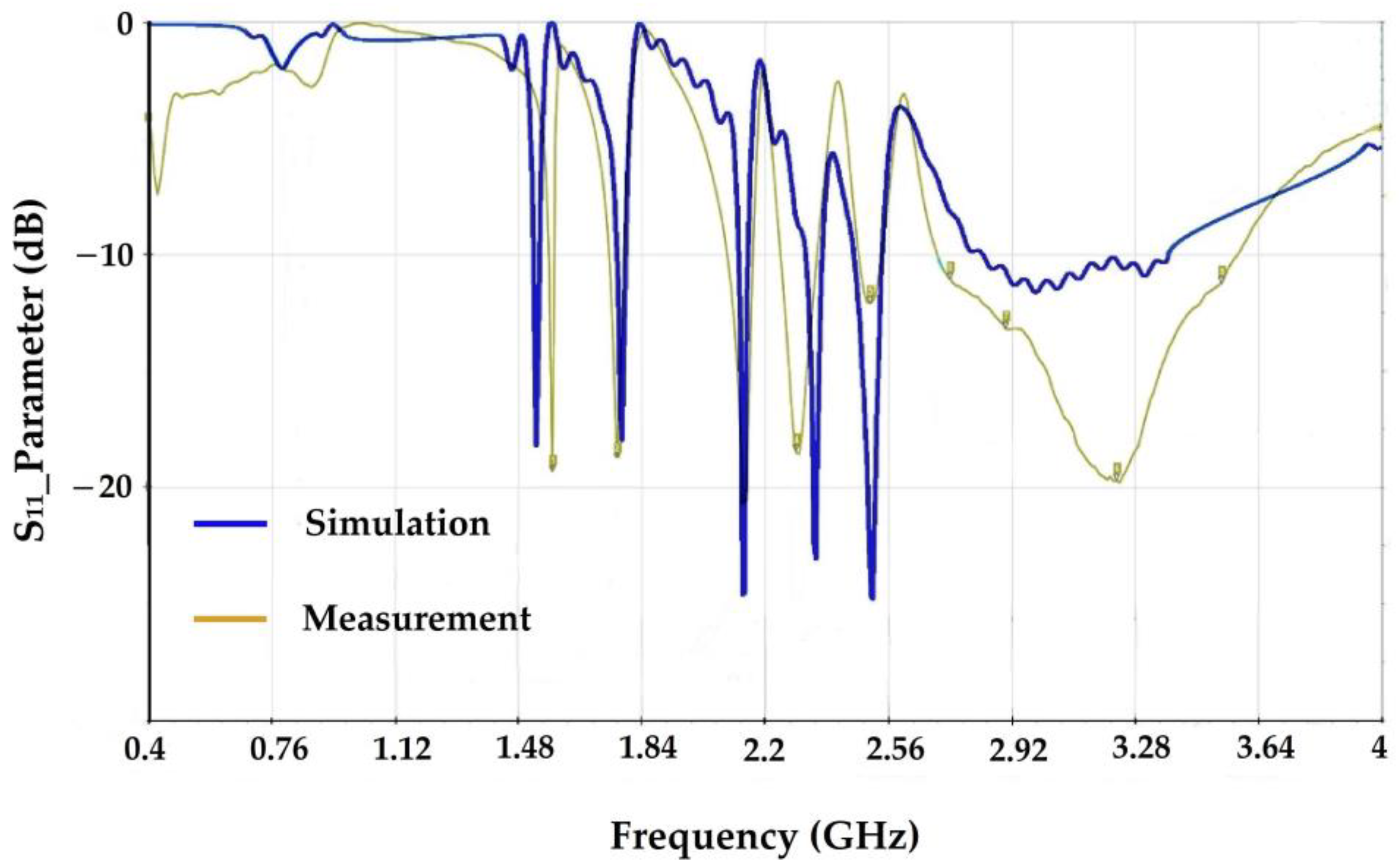
Figure 6.
The simulated and measured S11 parameter of the proposed antenna.
Figure 6.
The simulated and measured S11 parameter of the proposed antenna.
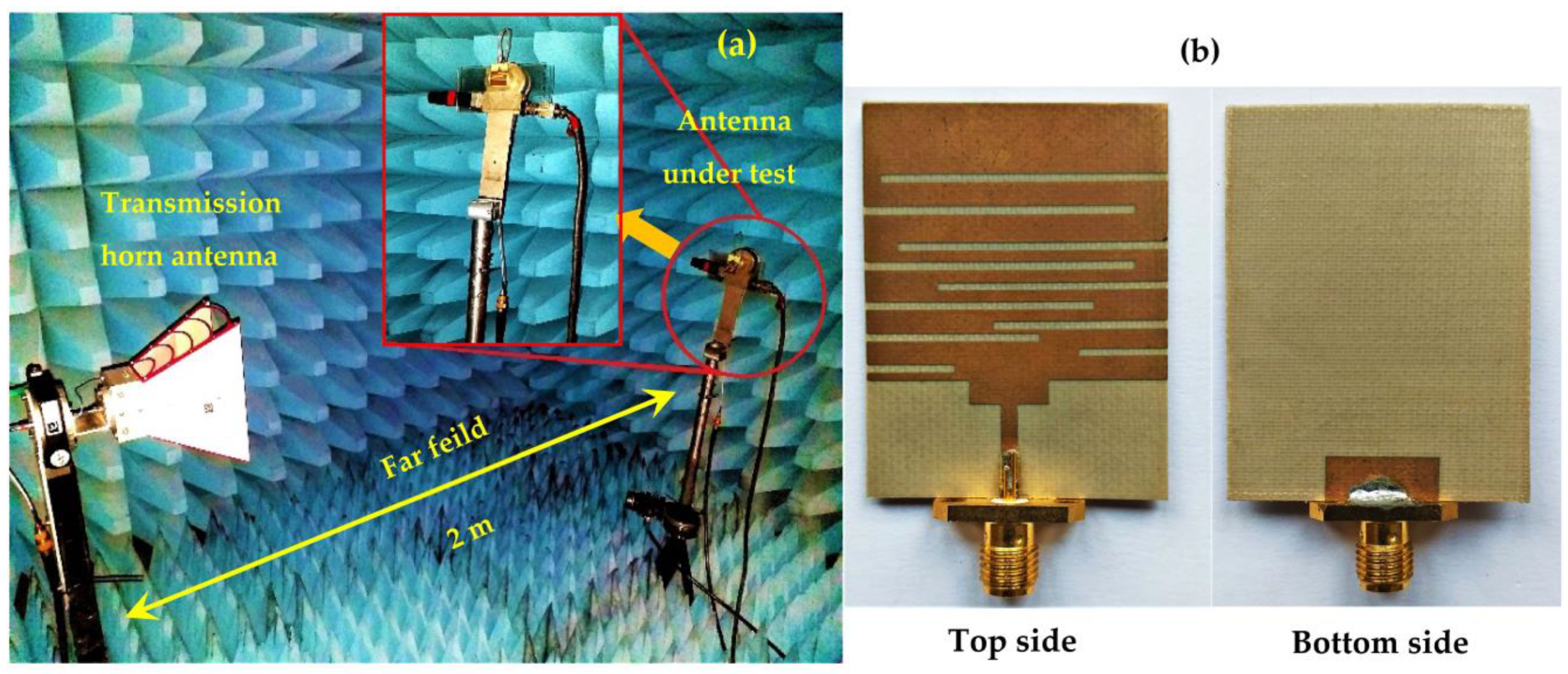
Figure 7.
(a) Measurement prototype and (b) realized antenna.
Figure 7.
(a) Measurement prototype and (b) realized antenna.
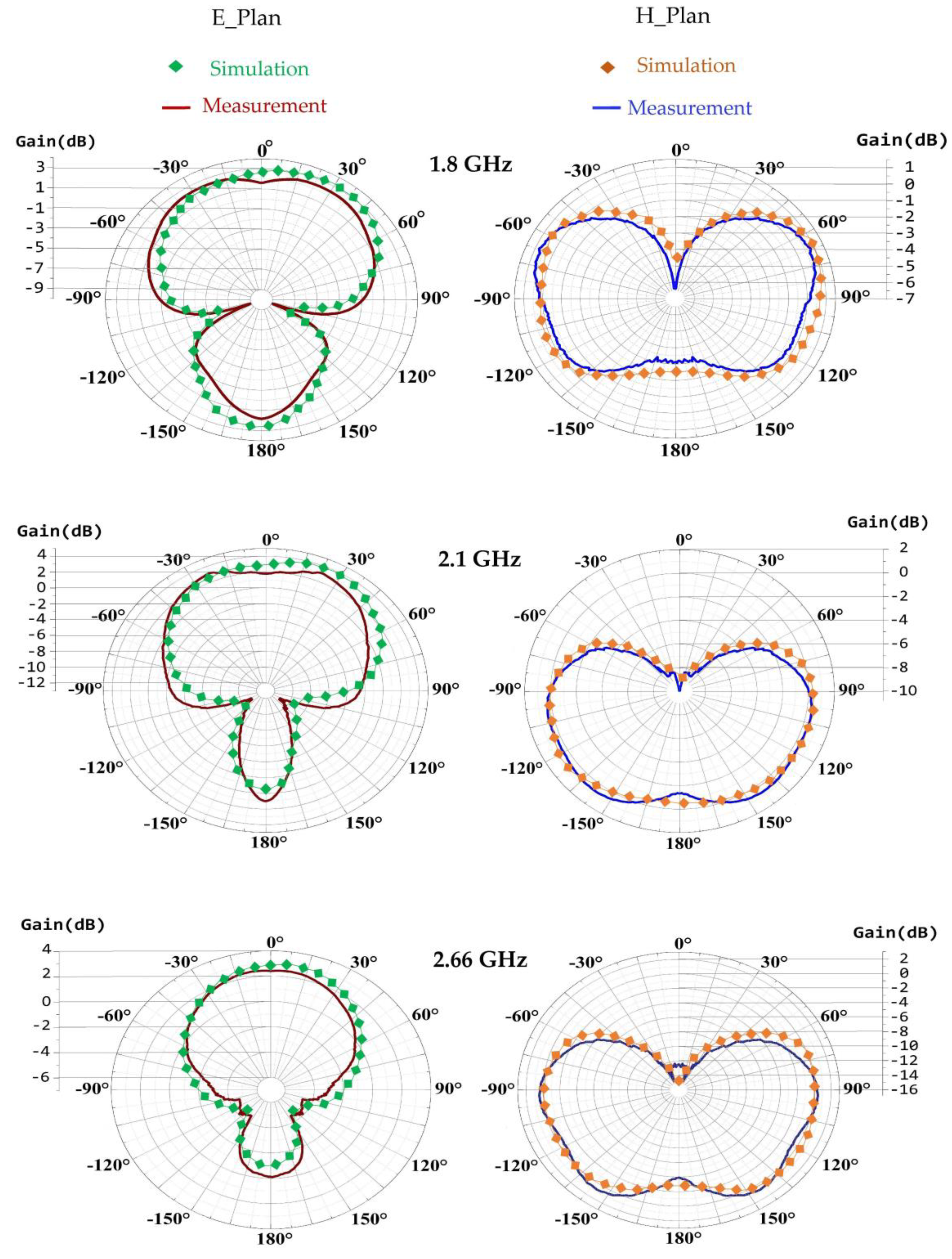
Figure 8.
Simulated and measured radiation pattern for GSM, UMTS, and LTE bands, respectively.
Figure 8.
Simulated and measured radiation pattern for GSM, UMTS, and LTE bands, respectively.
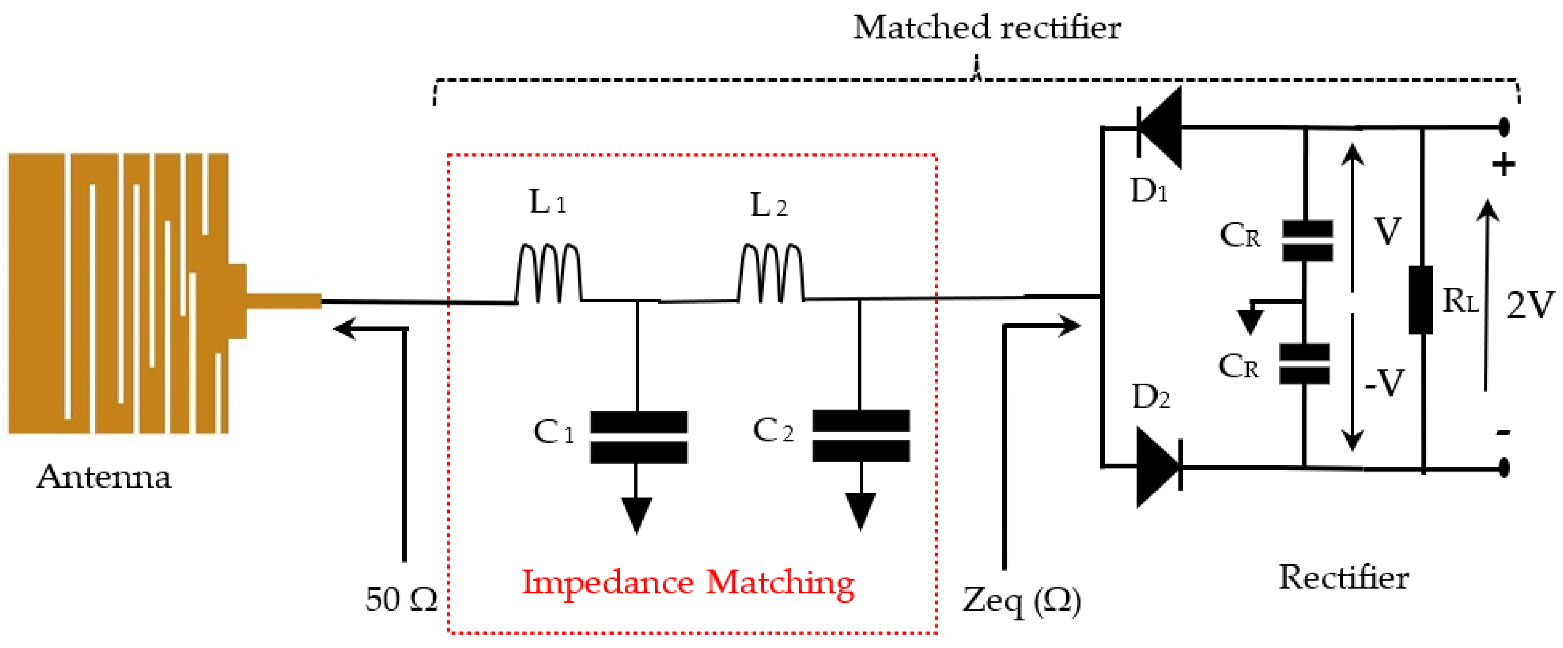
Figure 9.
Rectenna circuit with ideal impedance matching, D1, D2: (Schottky diodes: SMS7630-079LF), CR = 470 uF, RL = 2 kΩ.
Figure 9.
Rectenna circuit with ideal impedance matching, D1, D2: (Schottky diodes: SMS7630-079LF), CR = 470 uF, RL = 2 kΩ.
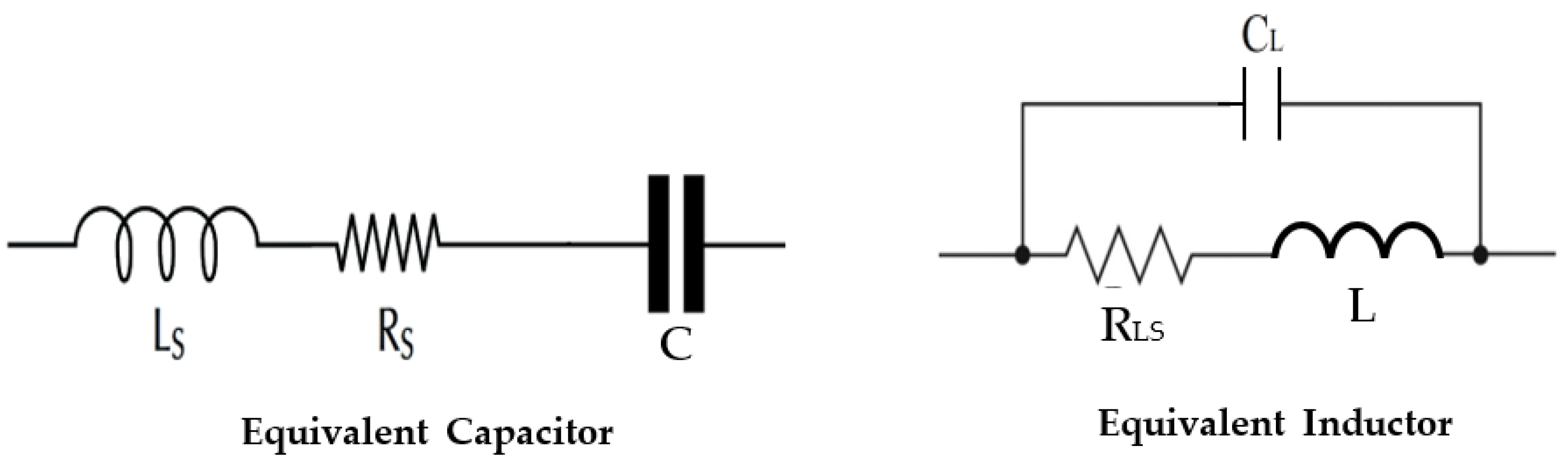
Figure 10.
Equivalent circuit of capacitor and inductor. Ls: Series inductance, Rs: Electrodes and terminations resistance, C: Capacitance, L: Inductor, CL: Parasitic capacitor, RLS: Intern resistor.
Figure 10.
Equivalent circuit of capacitor and inductor. Ls: Series inductance, Rs: Electrodes and terminations resistance, C: Capacitance, L: Inductor, CL: Parasitic capacitor, RLS: Intern resistor.
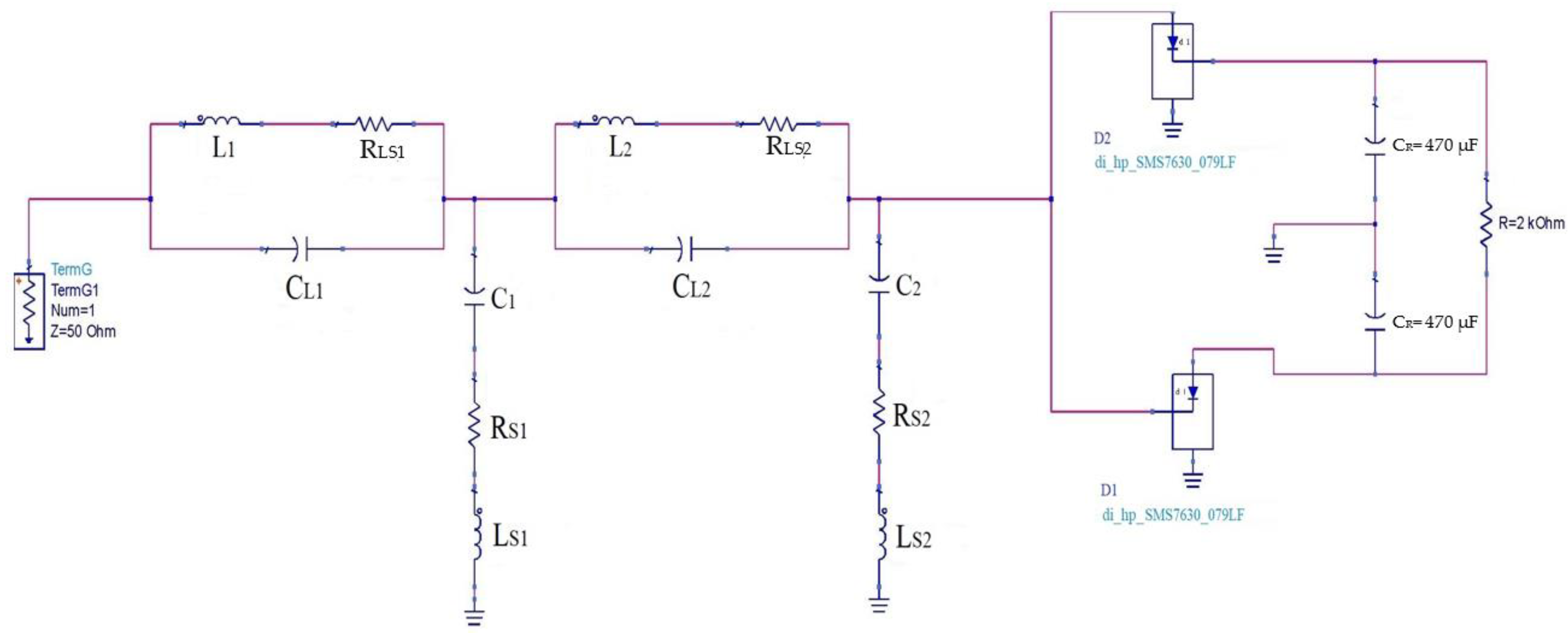
Figure 11.
Practical rectenna circuit with all parasitic elements.
Figure 11.
Practical rectenna circuit with all parasitic elements.
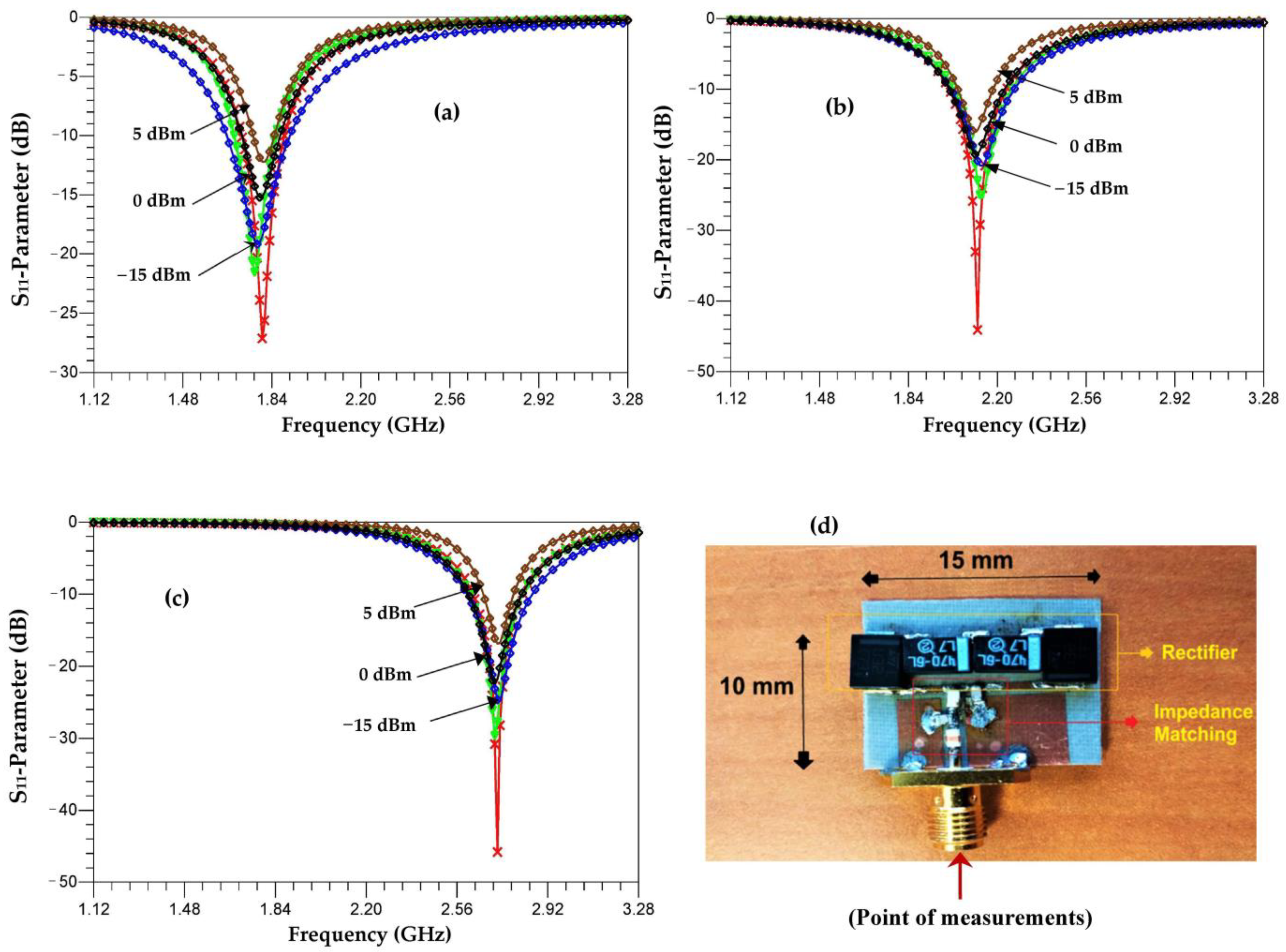
Figure 12.
Simulated and measured S
11 parameters of the three rectifiers for each frequency bands ((
a) 1.8 GHz, 2.1 GHz (
b) and 2.66 GHz (
c)) and realized prototype (
d).
![Sensors 22 03576 i001]()
Measurement,
![Sensors 22 03576 i002]()
Simulation
![Sensors 22 03576 i003]()
Co-simulation with parasitic elements.
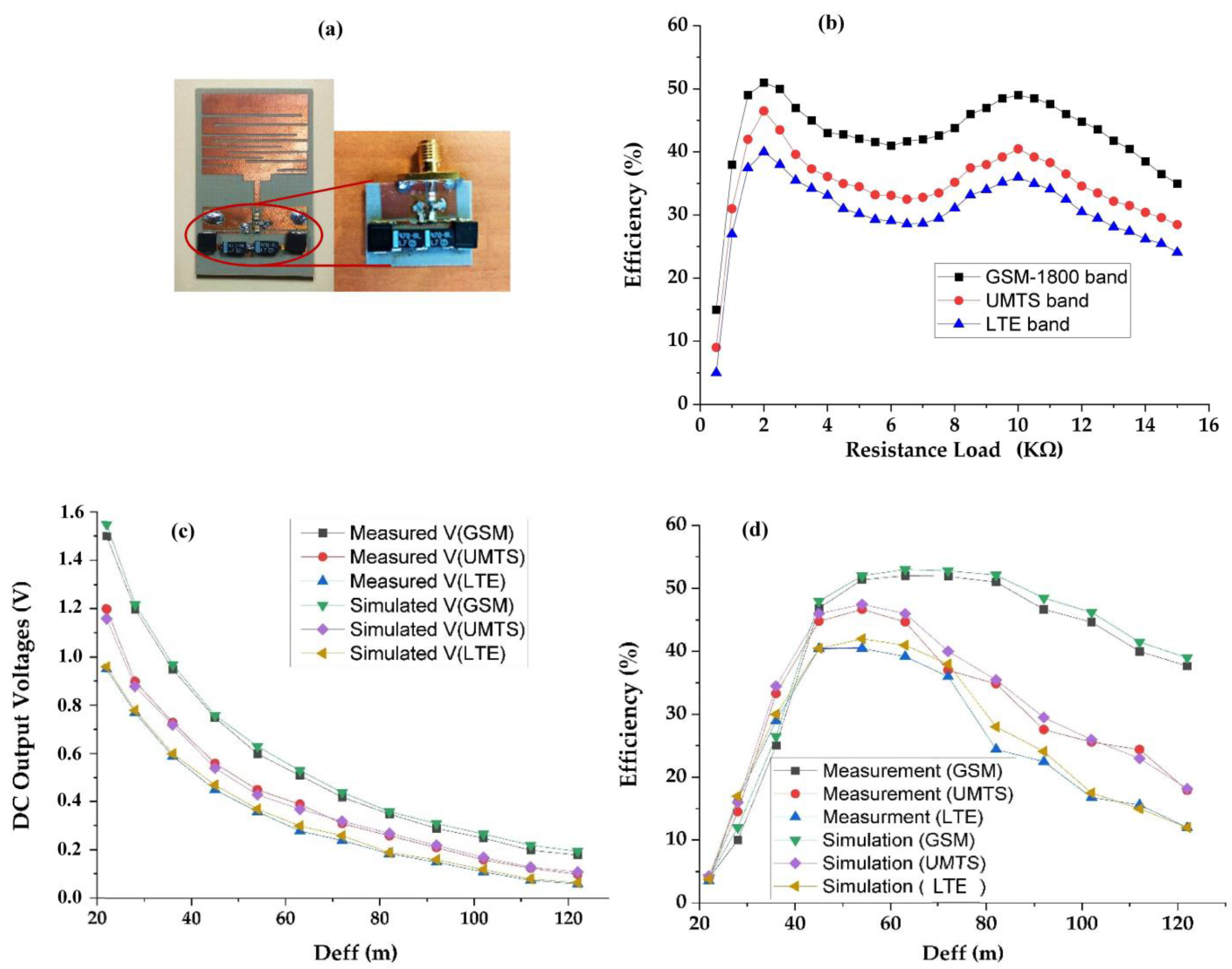
Figure 13.
(a) Realized rectenna prototype, (b) Efficiency variation versus resistance load at 54 m, and (c,d) simulated and measured DC output voltages and RF-to-DC conversion efficiency, respectively, for GSM-1800, UMTS, and LTE-2.6 bands for 2 kΩ resistance load.
Figure 13.
(a) Realized rectenna prototype, (b) Efficiency variation versus resistance load at 54 m, and (c,d) simulated and measured DC output voltages and RF-to-DC conversion efficiency, respectively, for GSM-1800, UMTS, and LTE-2.6 bands for 2 kΩ resistance load.
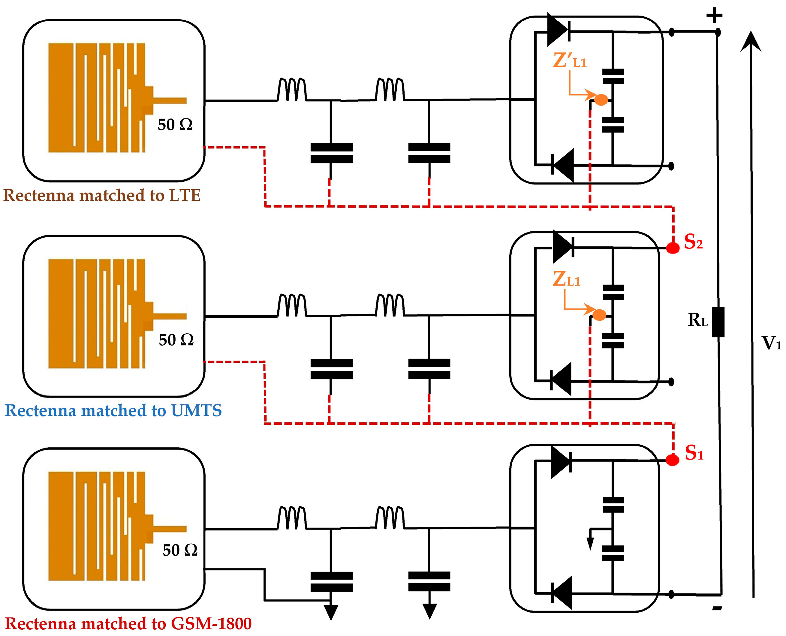
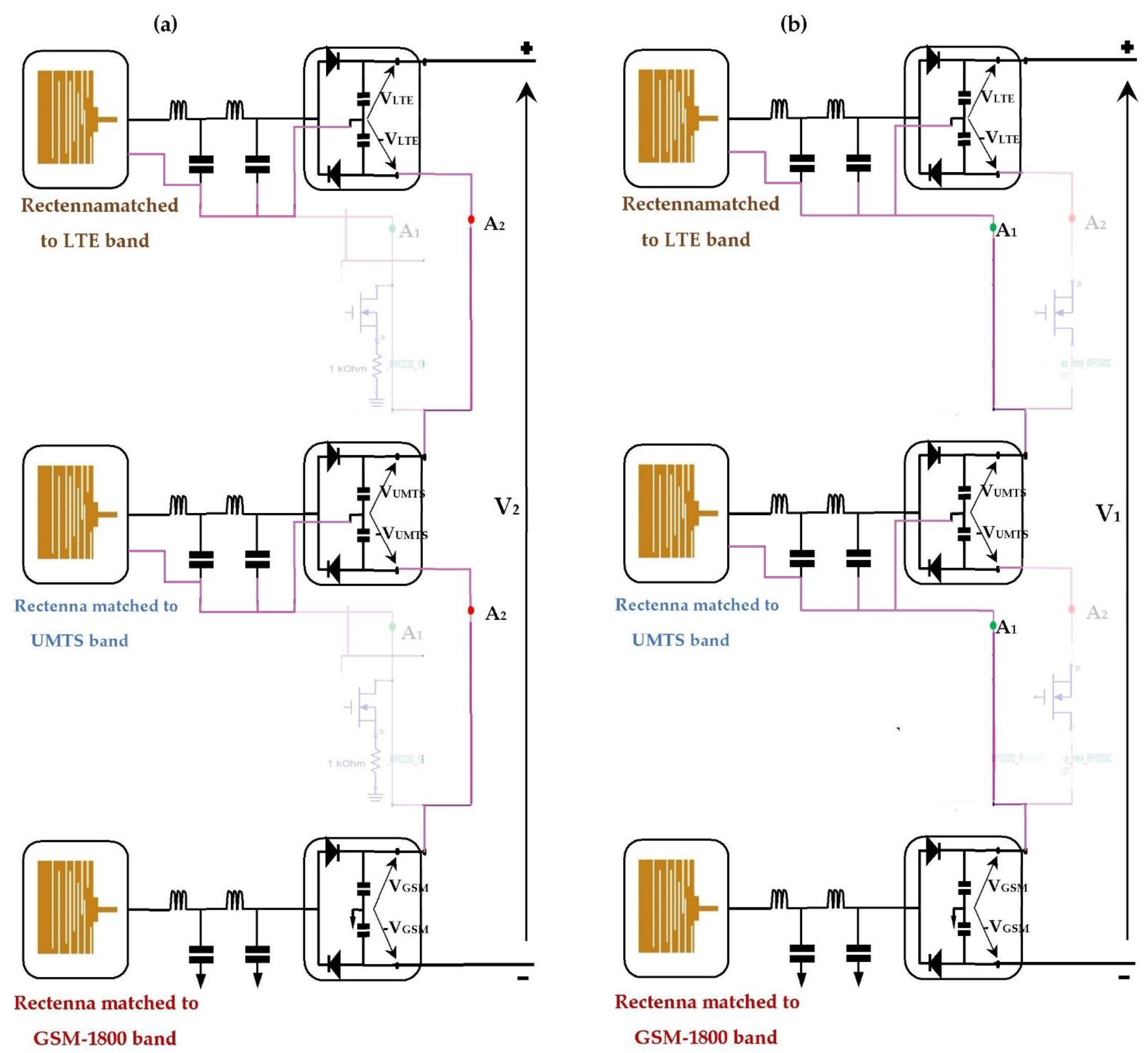
Figure 14.
First architecture with three rectennas matched to GSM-1800, UMTS, and LTE-2.6. ZL1, Z’L1 are the impedances at the selected points.
Figure 14.
First architecture with three rectennas matched to GSM-1800, UMTS, and LTE-2.6. ZL1, Z’L1 are the impedances at the selected points.
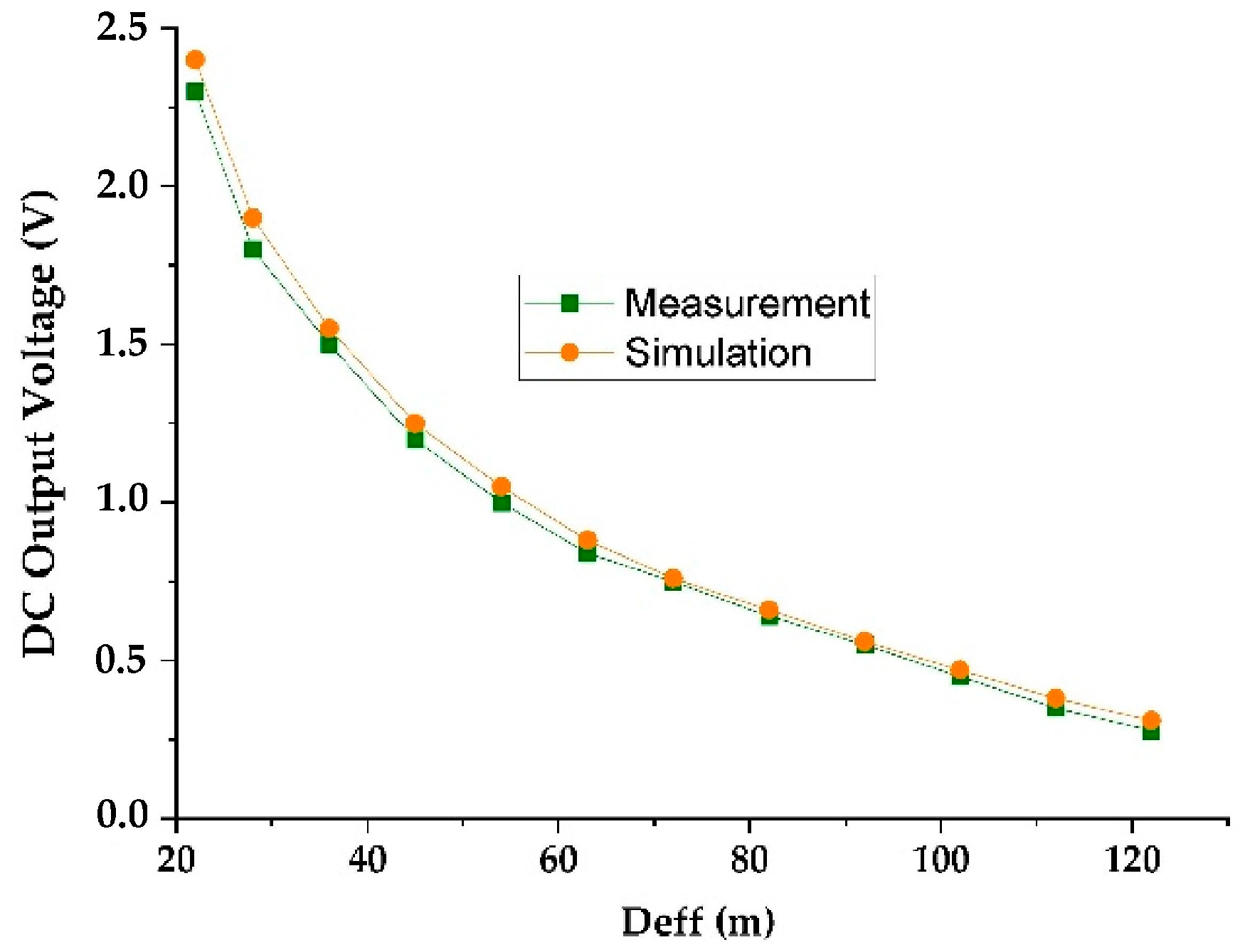
Figure 15.
Simulated and measured DC output voltage for 2 kΩ resistance load.
Figure 15.
Simulated and measured DC output voltage for 2 kΩ resistance load.
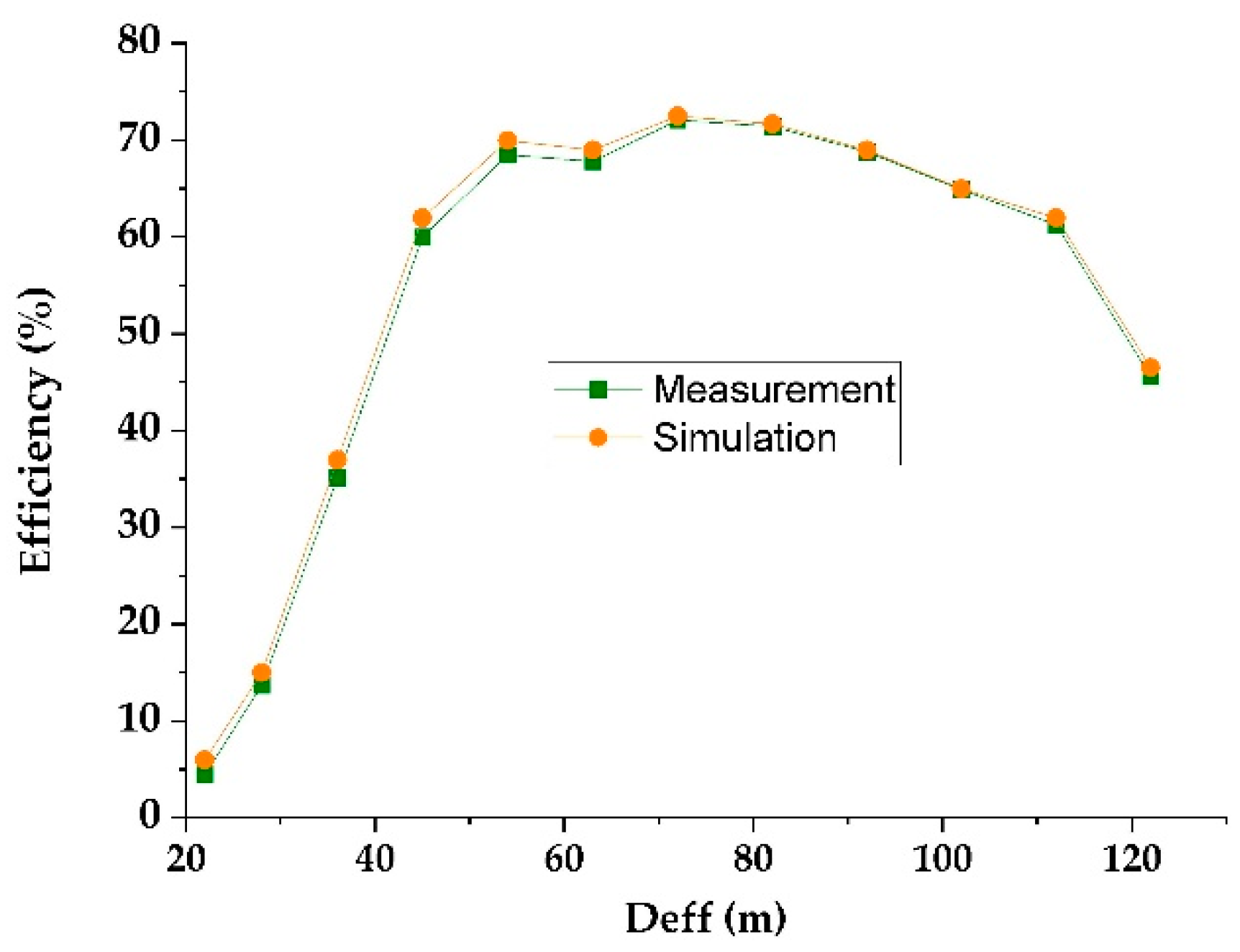
Figure 16.
Simulated and measured RF-to-DC conversion efficiency for 2 kΩ resistance load.
Figure 16.
Simulated and measured RF-to-DC conversion efficiency for 2 kΩ resistance load.
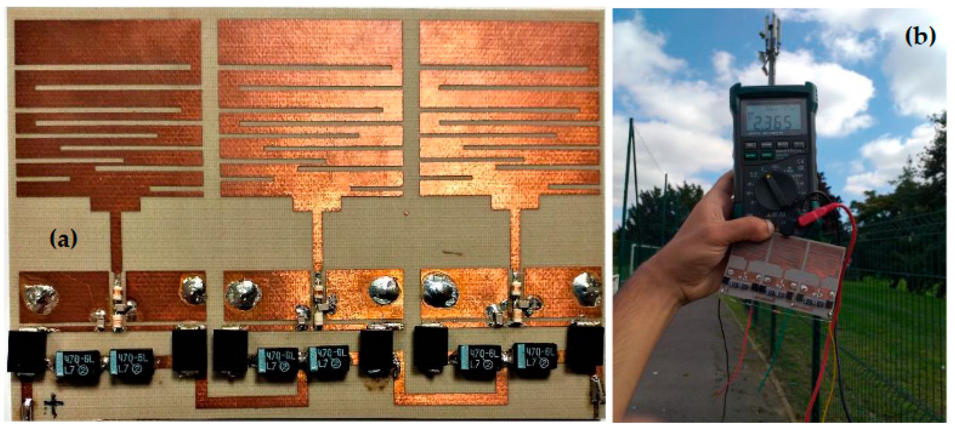
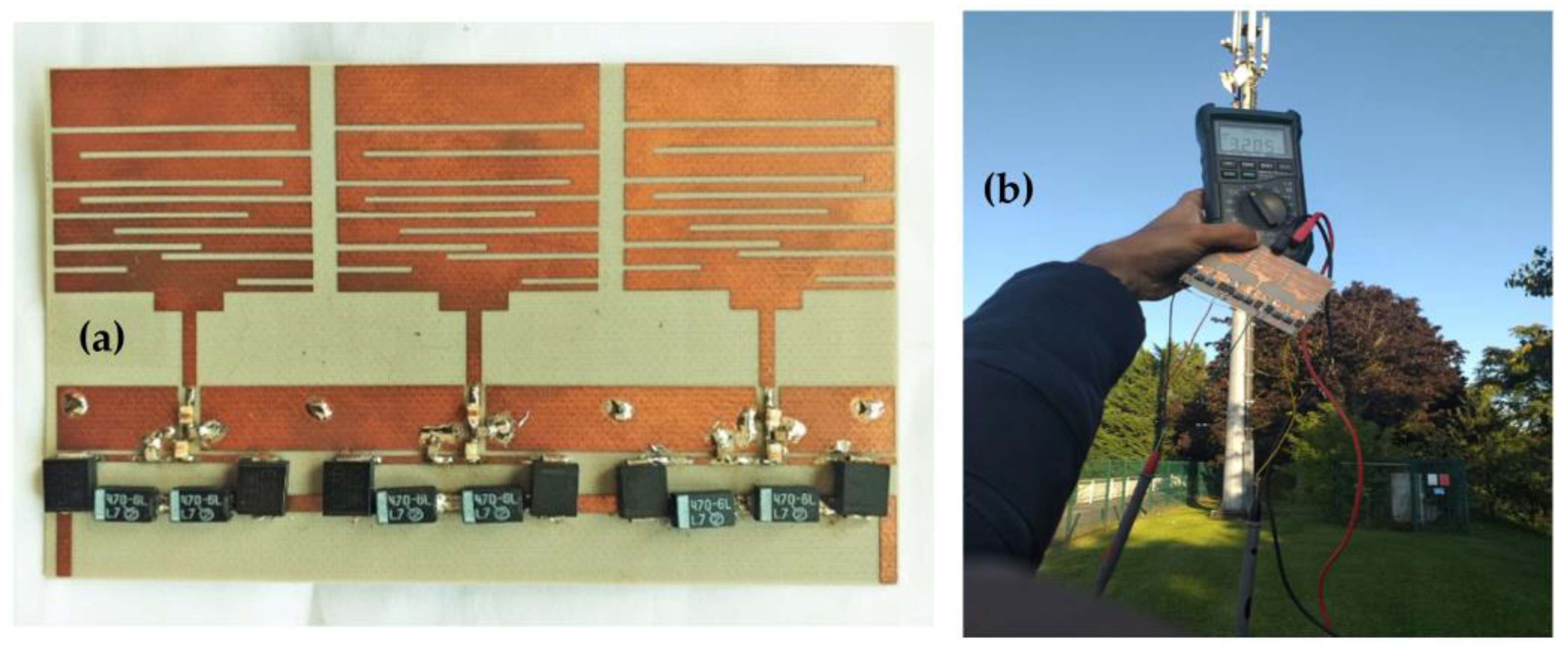
Figure 17.
(a) Realized RF-EH1 based on the first architecture, (b) Measurement prototype at 22 m from relay antenna.
Figure 17.
(a) Realized RF-EH1 based on the first architecture, (b) Measurement prototype at 22 m from relay antenna.
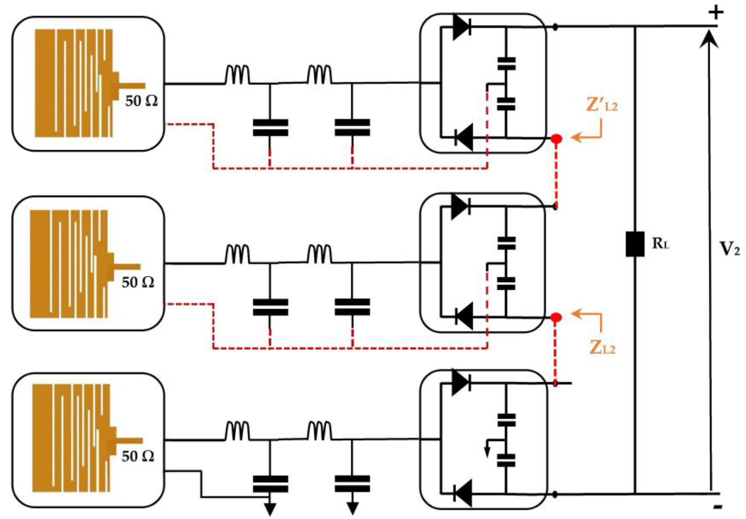
Figure 18.
Second architecture with three rectennas matched to GSM-1800, UMTS, and LTE-2.6. ZL2, Z’L2 are the impedances at the selected points.
Figure 18.
Second architecture with three rectennas matched to GSM-1800, UMTS, and LTE-2.6. ZL2, Z’L2 are the impedances at the selected points.
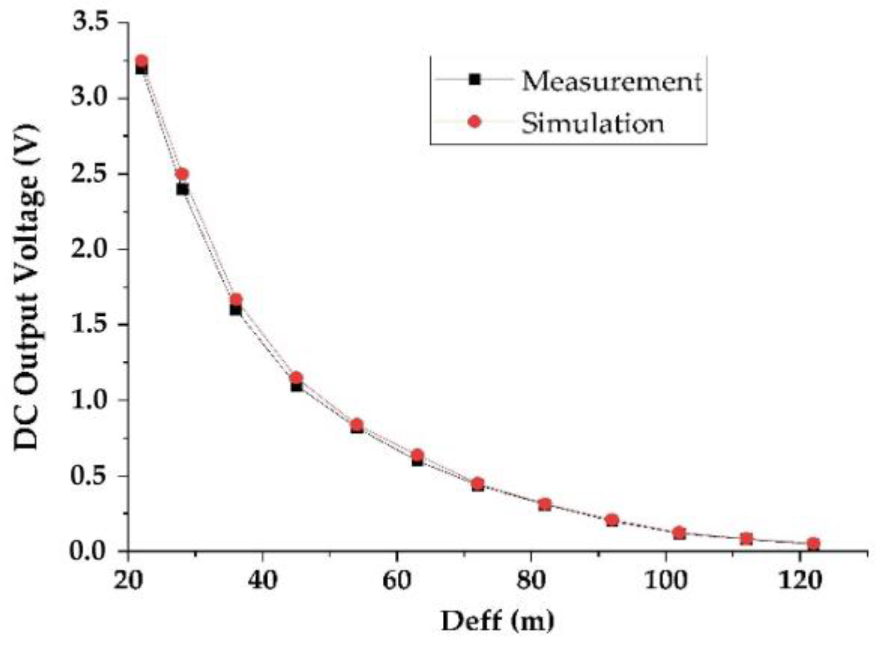
Figure 19.
Measured and simulated DC output voltage as a function of the effective distance for 2 kΩ resistance load.
Figure 19.
Measured and simulated DC output voltage as a function of the effective distance for 2 kΩ resistance load.
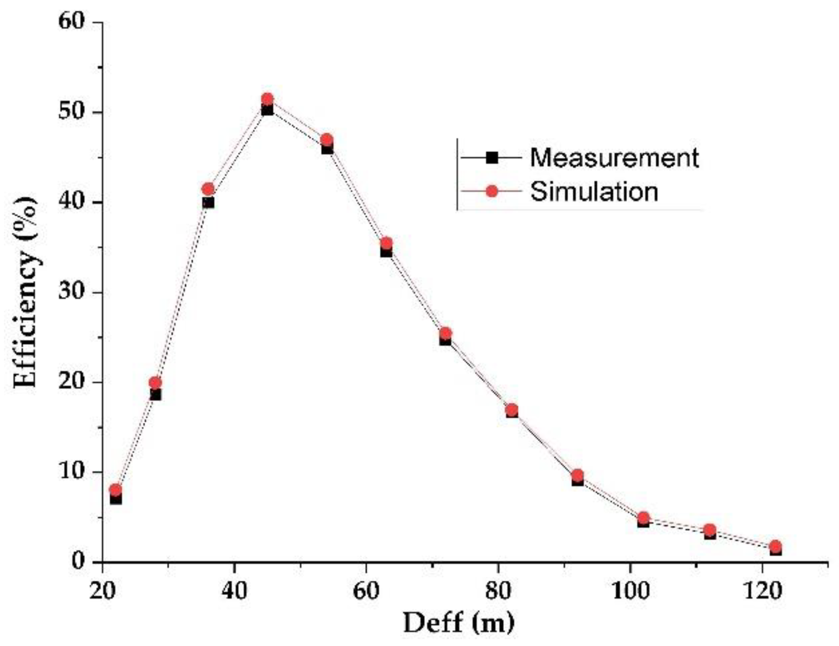
Figure 20.
Measured and simulated efficiencies provided by the second architecture for 2 kΩ resistance load.
Figure 20.
Measured and simulated efficiencies provided by the second architecture for 2 kΩ resistance load.
Figure 21.
(a) Realized RF-EH2, (b) Prototype of measurement at 22 m from relay antenna.
Figure 21.
(a) Realized RF-EH2, (b) Prototype of measurement at 22 m from relay antenna.
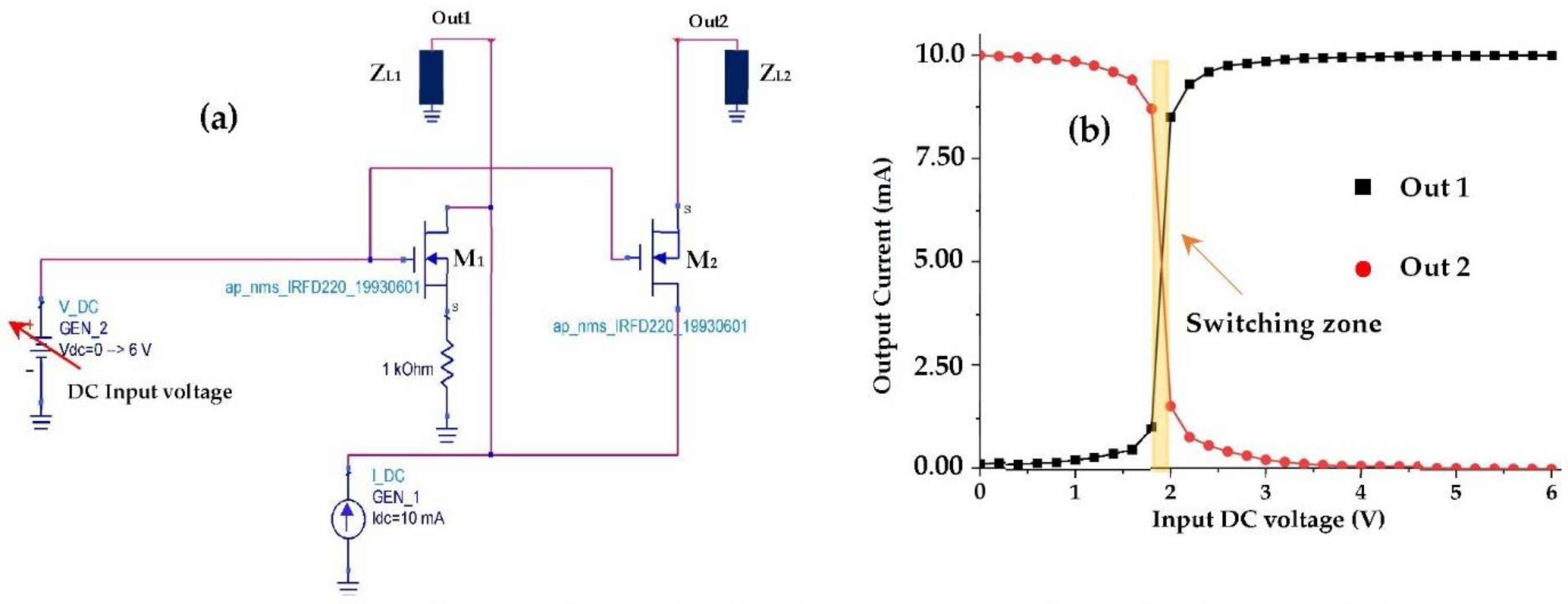
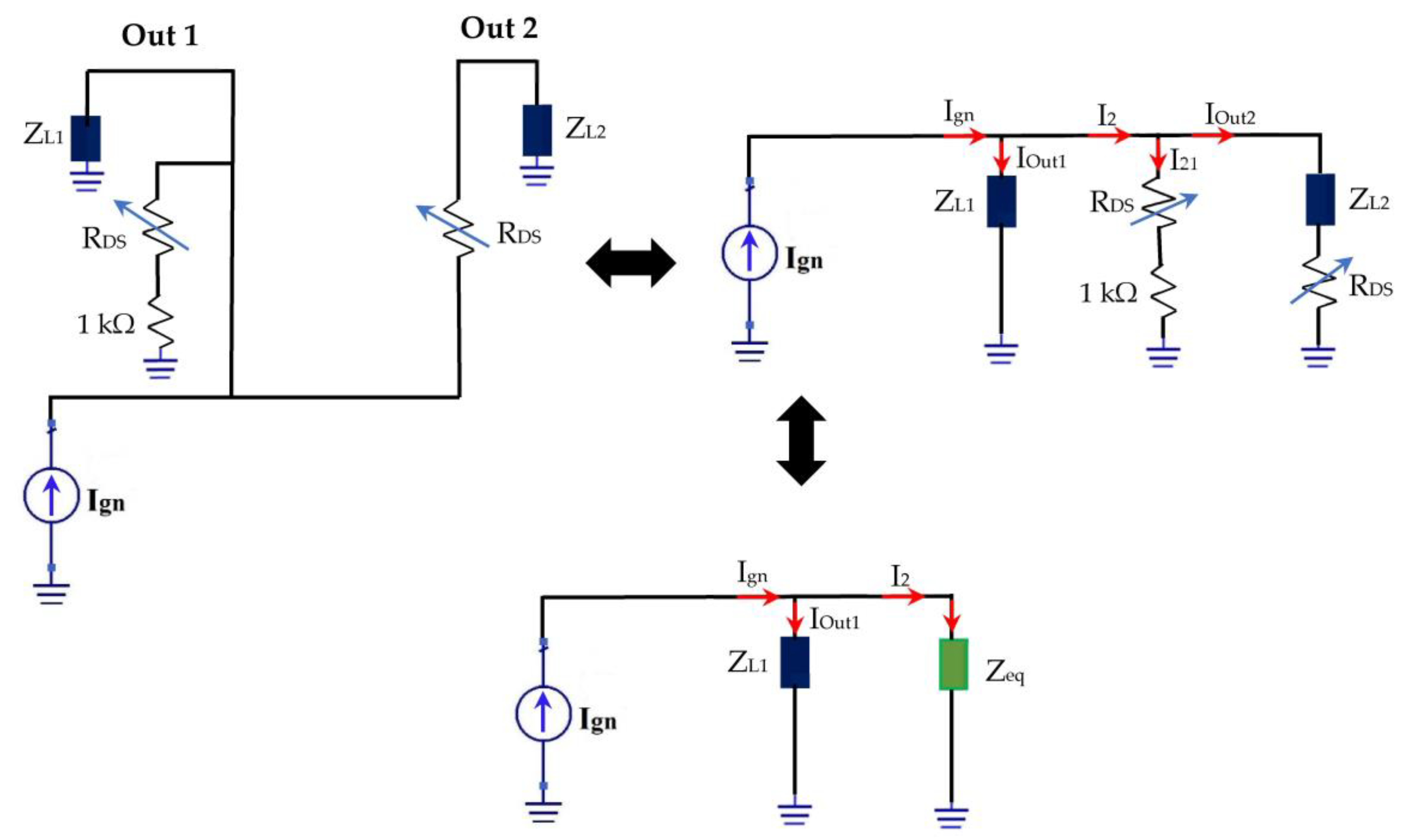
Figure 22.
(a) Proposed switch circuit, (b) Simulated DC output currents (Out1, Out2). ZL1 = 7.2 kΩ, ZL2 = 0.1 Ω.
Figure 22.
(a) Proposed switch circuit, (b) Simulated DC output currents (Out1, Out2). ZL1 = 7.2 kΩ, ZL2 = 0.1 Ω.
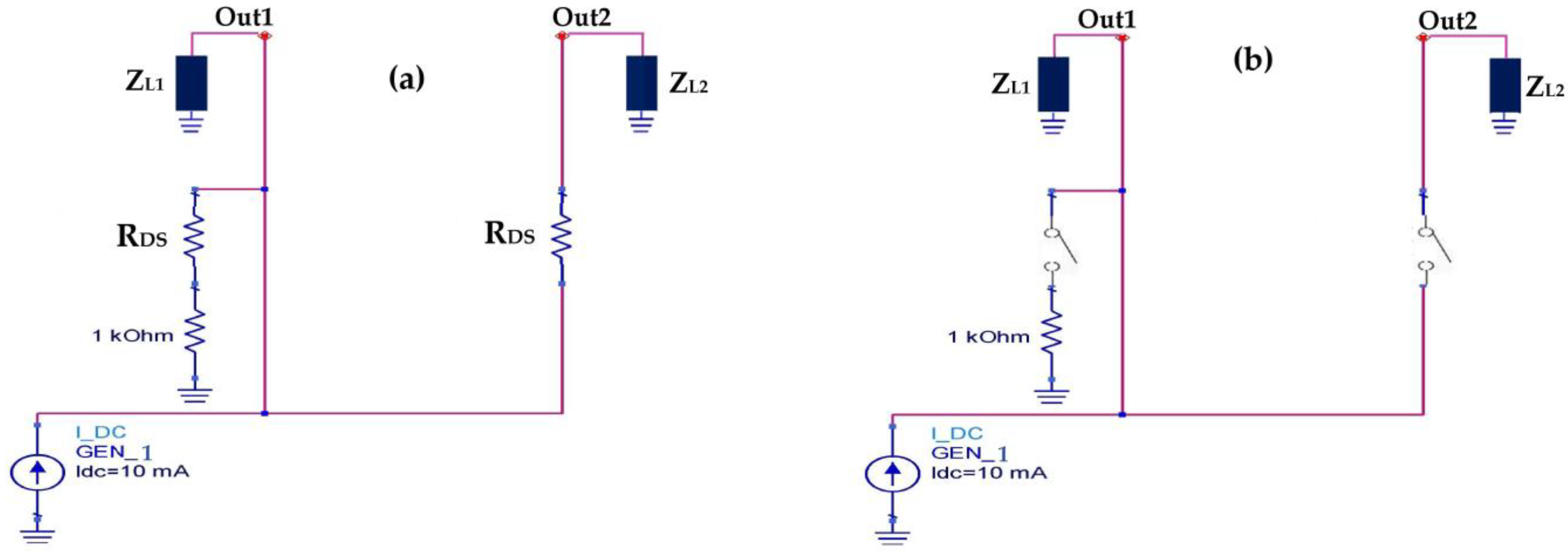
Figure 23.
(a) Equivalent circuit for high input powers, (b) Equivalent circuit for low input powers.
Figure 23.
(a) Equivalent circuit for high input powers, (b) Equivalent circuit for low input powers.
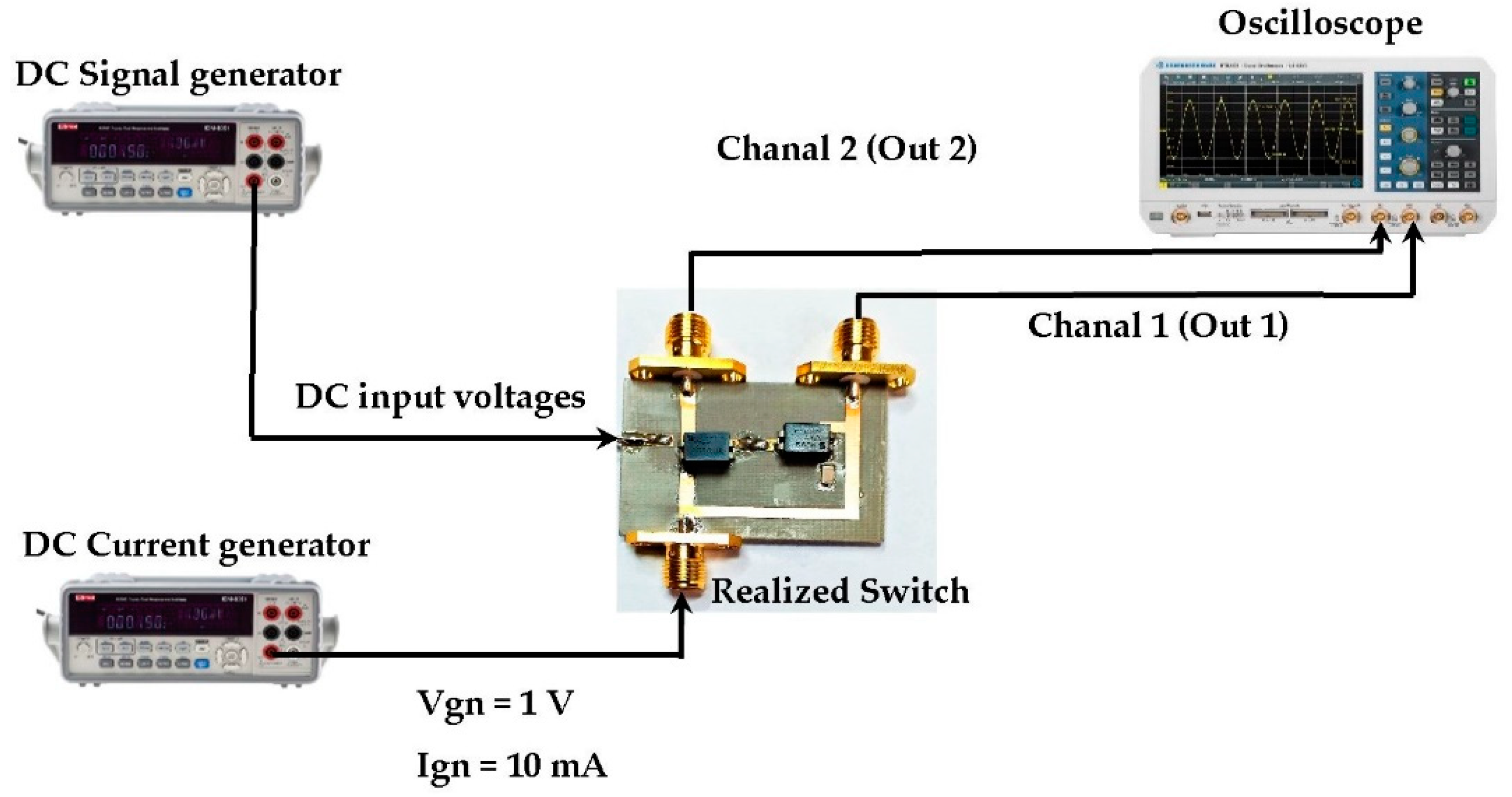
Figure 24.
Measurement prototype of the output currents for the first and second outputs of the proposed switch.
Figure 24.
Measurement prototype of the output currents for the first and second outputs of the proposed switch.
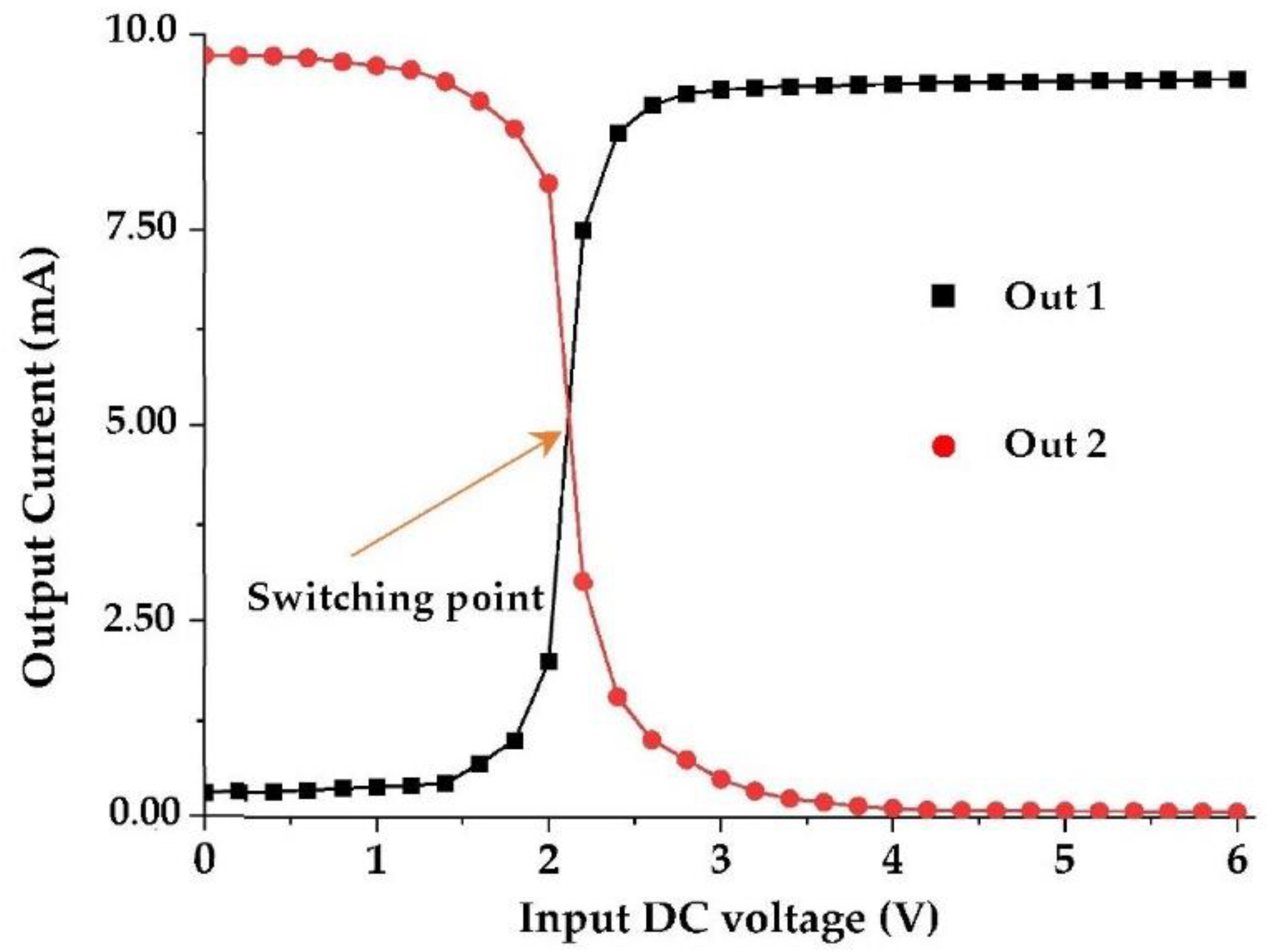
Figure 25.
Measured DC output currents (Out1, Out2) of the proposed switch.
Figure 25.
Measured DC output currents (Out1, Out2) of the proposed switch.
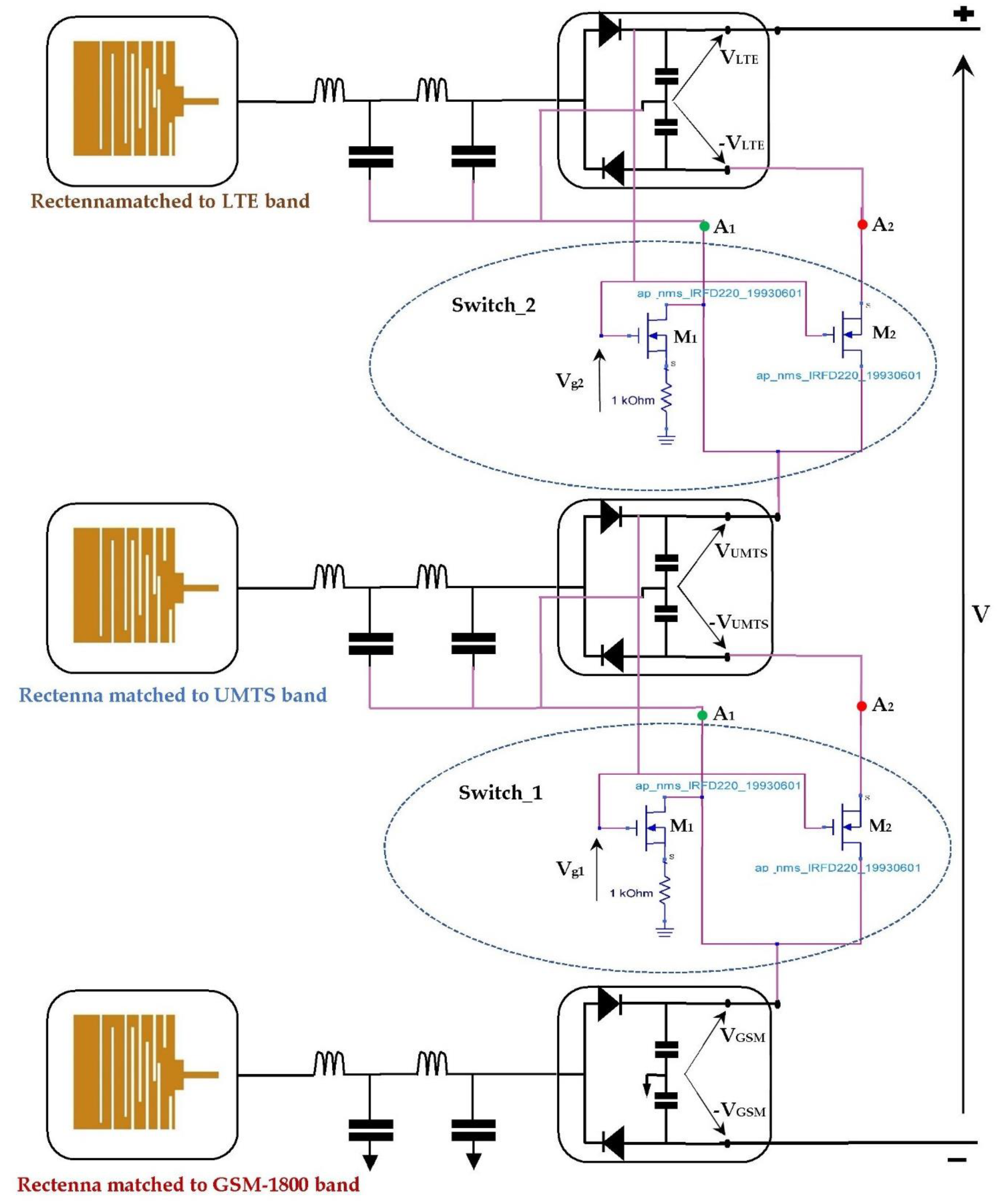
Figure 26.
Proposed RF-EH system combining both previous architectures using the studied switch. A1 and A2 are the two positions corresponding to first and second architectures.
Figure 26.
Proposed RF-EH system combining both previous architectures using the studied switch. A1 and A2 are the two positions corresponding to first and second architectures.
Figure 27.
Switching between both previous architectures according to the input power levels. (a) for high input power levels, (b) for low input power levels.
Figure 27.
Switching between both previous architectures according to the input power levels. (a) for high input power levels, (b) for low input power levels.
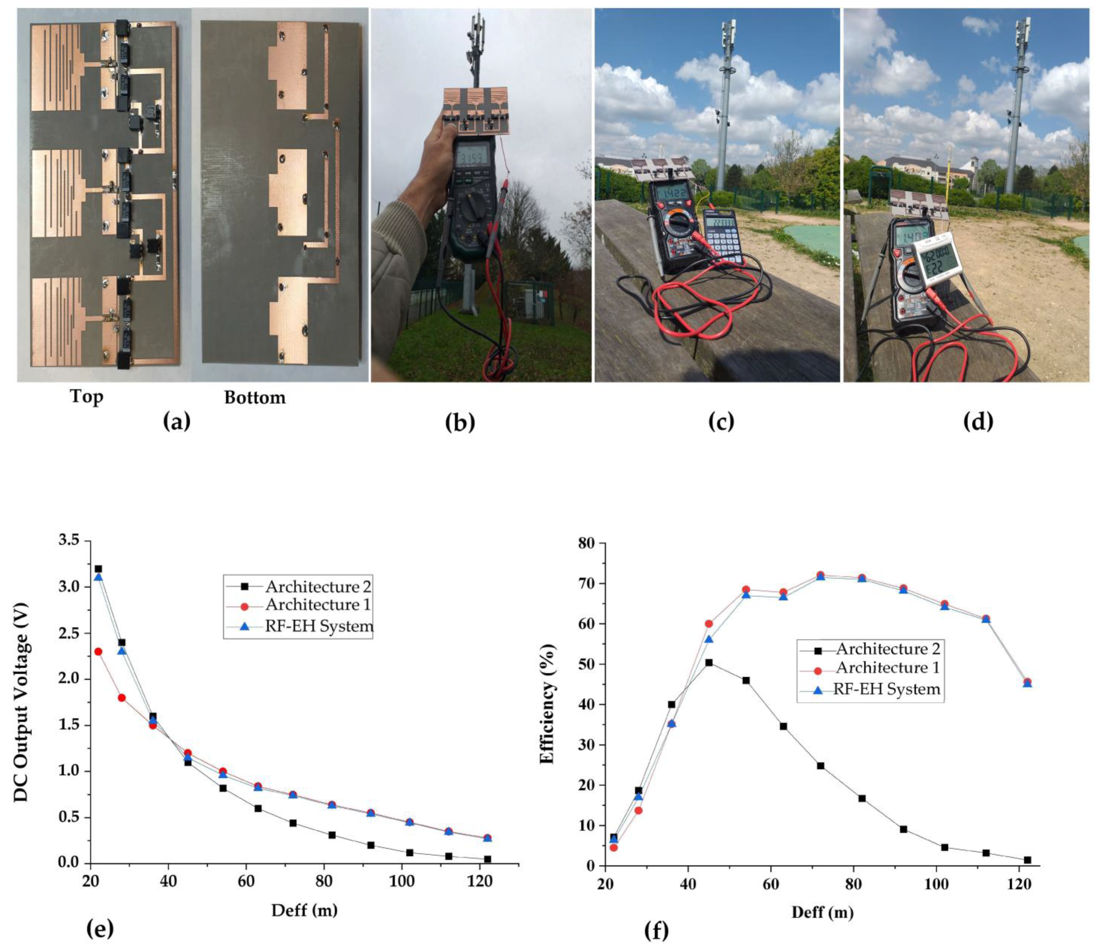
Figure 28.
Measurements results: (a) realized proposed RF-EH system, (b) prototype of measurements, (c) Application of the proposed RF-EH system to feed digital calculate at 38 m from relay antenna, (d) Application of the proposed RF-EH system to feed temperature sensor at the same distance, (e) Measured DC output voltages, and (f) Measured RF-to-DC conversion efficiency.
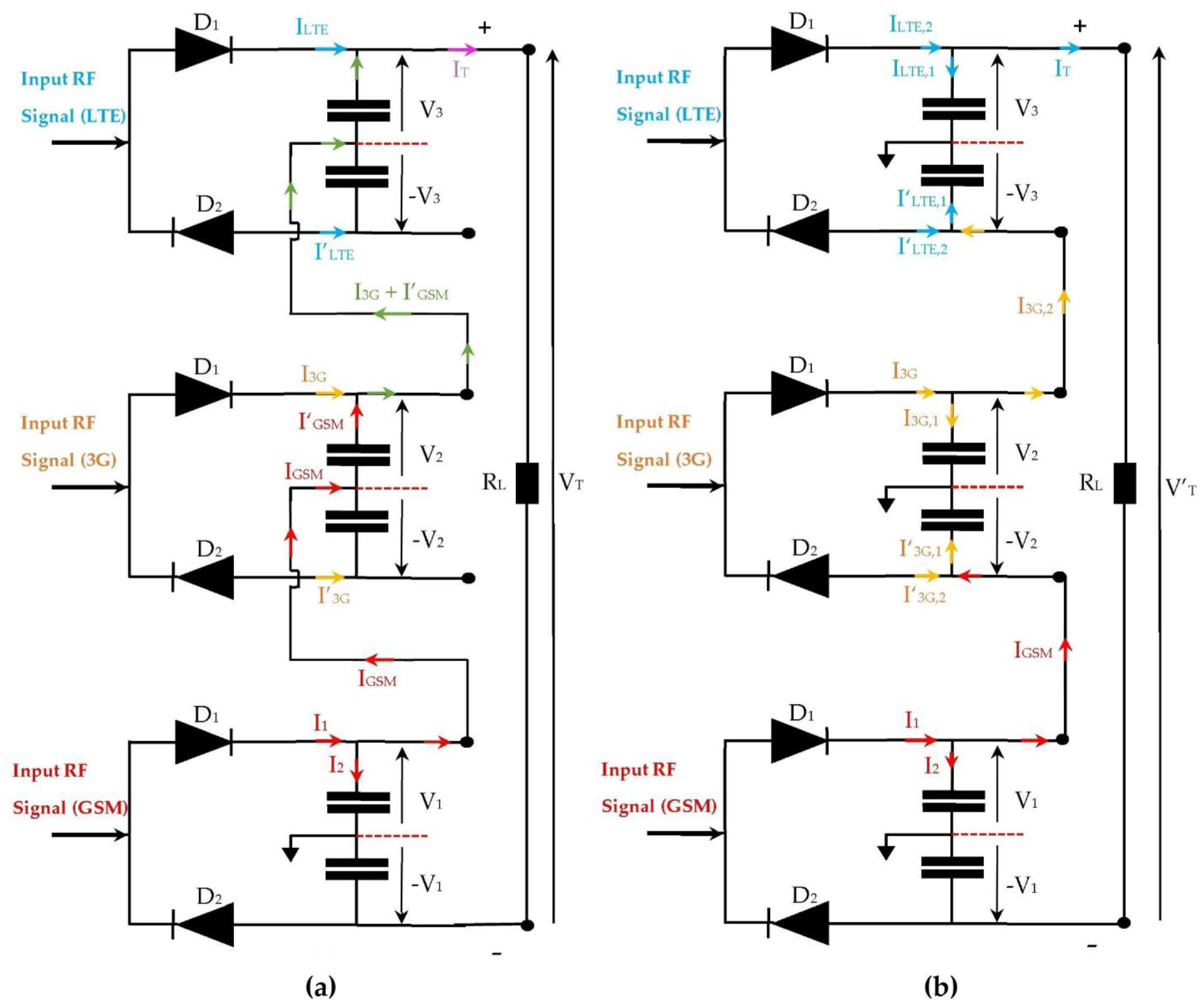
Figure 29.
Current flow for both architectures. (a) First architecture, (b) Second architecture.
Figure 29.
Current flow for both architectures. (a) First architecture, (b) Second architecture.
Figure 30.
Electrical representation of the proposed switch.
Figure 30.
Electrical representation of the proposed switch.
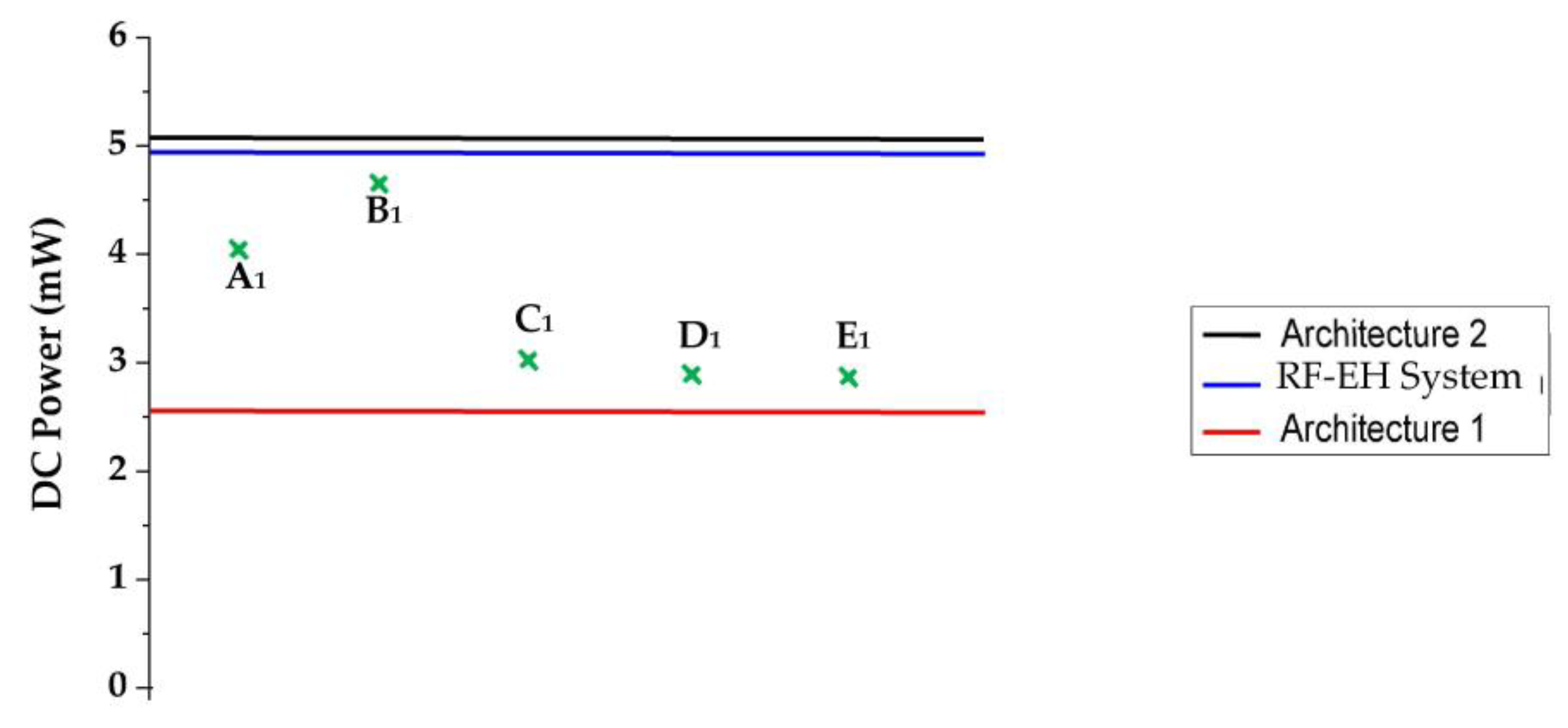
Figure 31.
Feeding ability of the system and both architectures at 22 m from relay antenna compared to minimum required power supply of the gas sensors. The DC powers A
1, B
1, C
1, D
1 and E
1 correspond to the power supply of sensors given in the references [
26,
27,
28,
29,
30], respectively.
Figure 31.
Feeding ability of the system and both architectures at 22 m from relay antenna compared to minimum required power supply of the gas sensors. The DC powers A
1, B
1, C
1, D
1 and E
1 correspond to the power supply of sensors given in the references [
26,
27,
28,
29,
30], respectively.
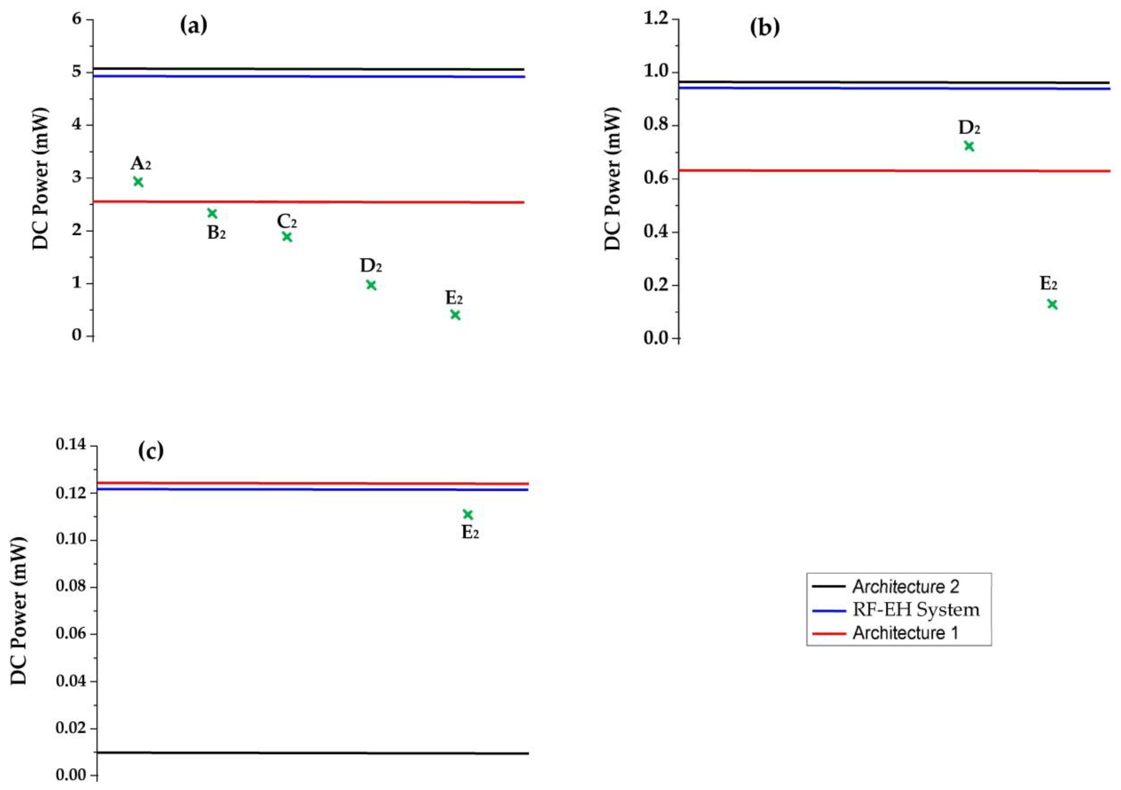
Figure 32.
Feeding ability of the RF-EH system and architectures at (
a): 22 m, (
b): 40 m, and (
c): 110 m from relay antenna compared to minimum required power supply of the image sensors. The DC powers A
2, B
2, C
2, D
2 and E
2 correspond to the power supply of sensors proposed in the references [
31,
32,
33,
34,
35], respectively.
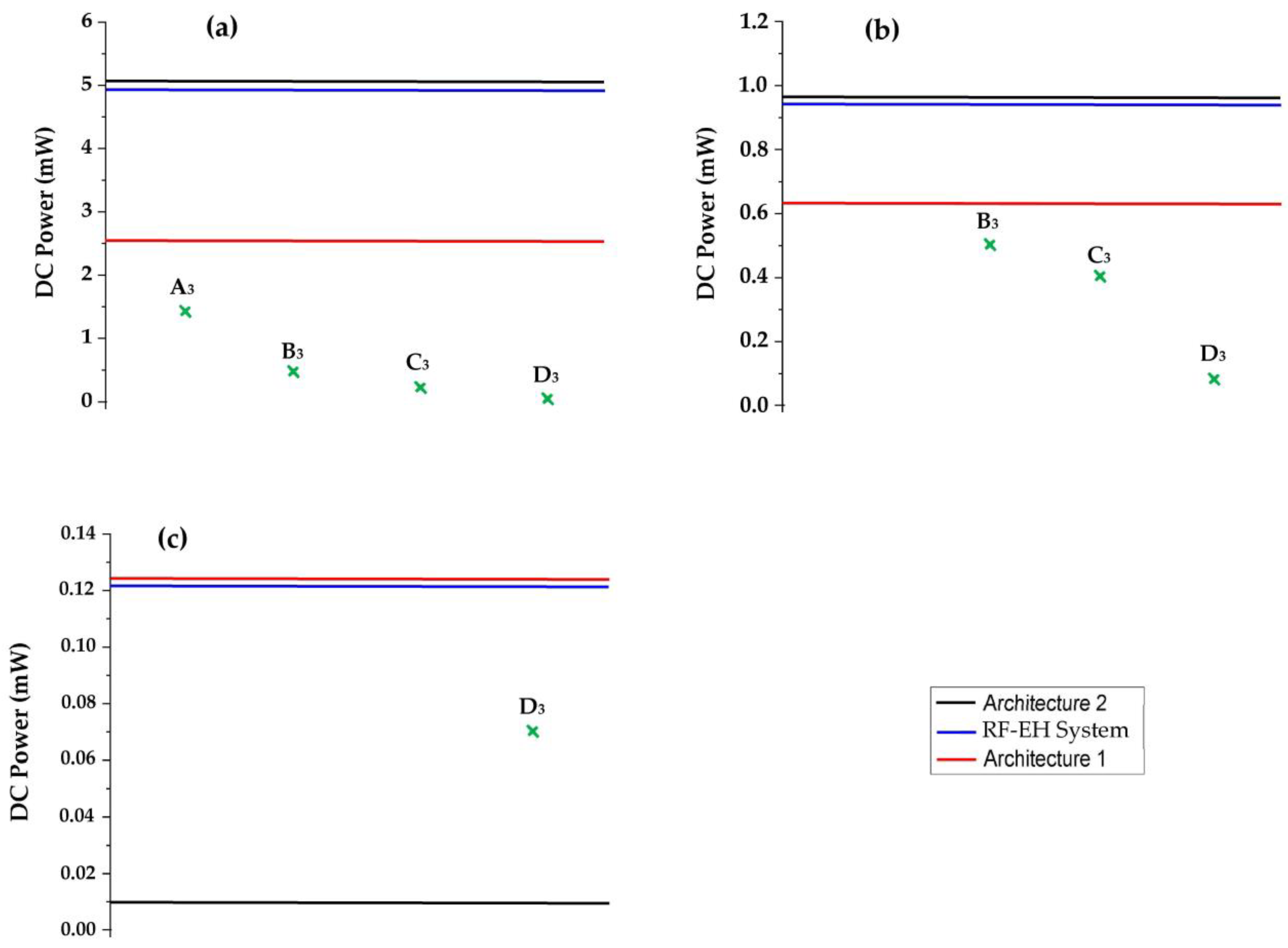
Figure 33.
Feeding ability of the RF-EH system and architectures at (
a): 22 m, (
b): 40 m, and (
c): 110 m from relay antenna compared to minimum required power supply of the pressure sensors. The DC powers A
3, B
3, C
3 and D
3 correspond to the power supply of sensors cited in the references [
36,
37,
38,
39], respectively.
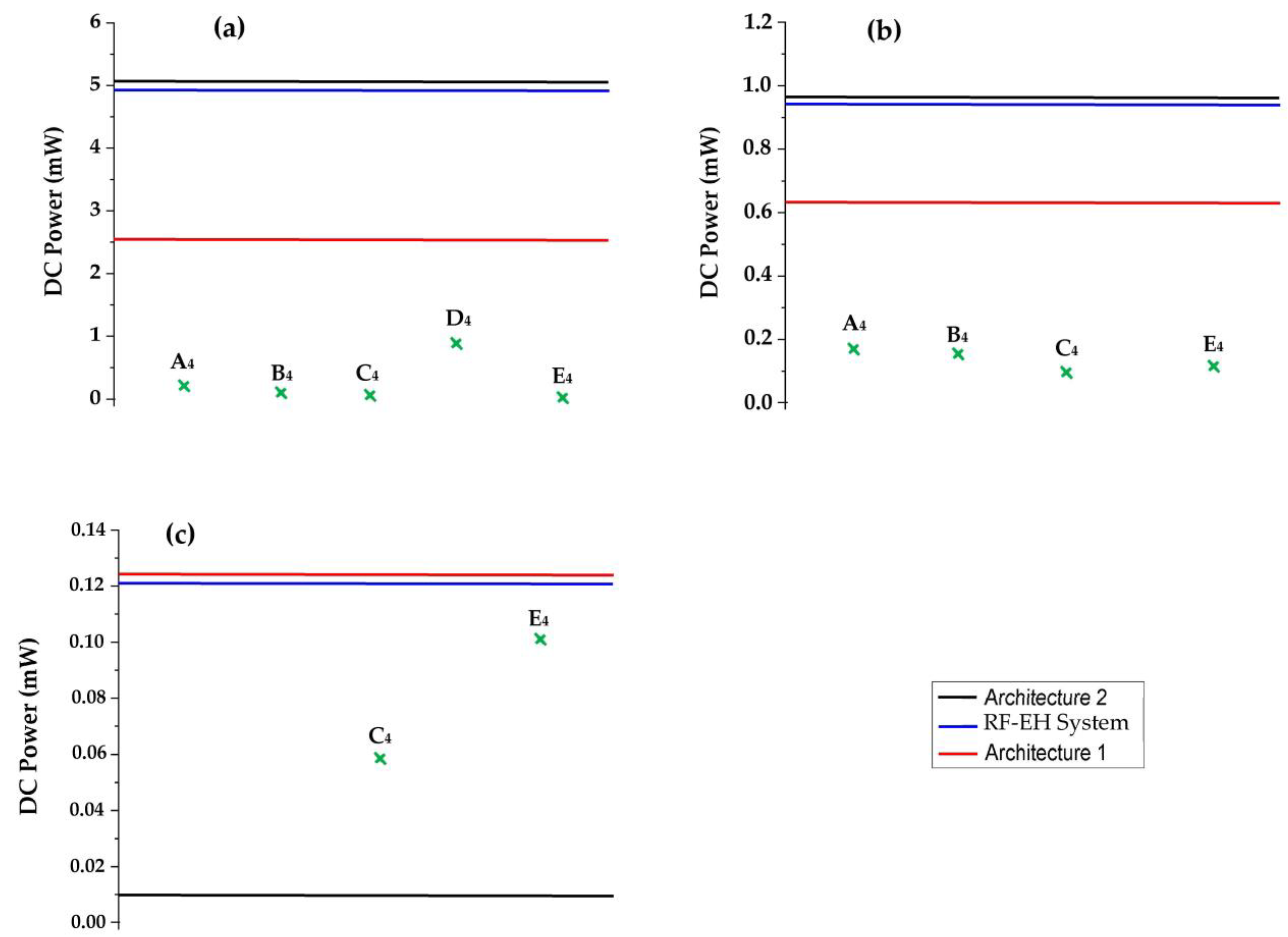
Figure 34.
Feeding ability of the RF-EH system and architectures at (
a): 22 m, (
b): 40 m, and (
c): 110 m from relay antenna compared to minimum required power supply of the biomedical sensors. The DC powers A
4, B
4, C
4, D
4 and E
4 correspond to the power supply of sensors presented in the references [
40,
41,
42,
43,
44], respectively.
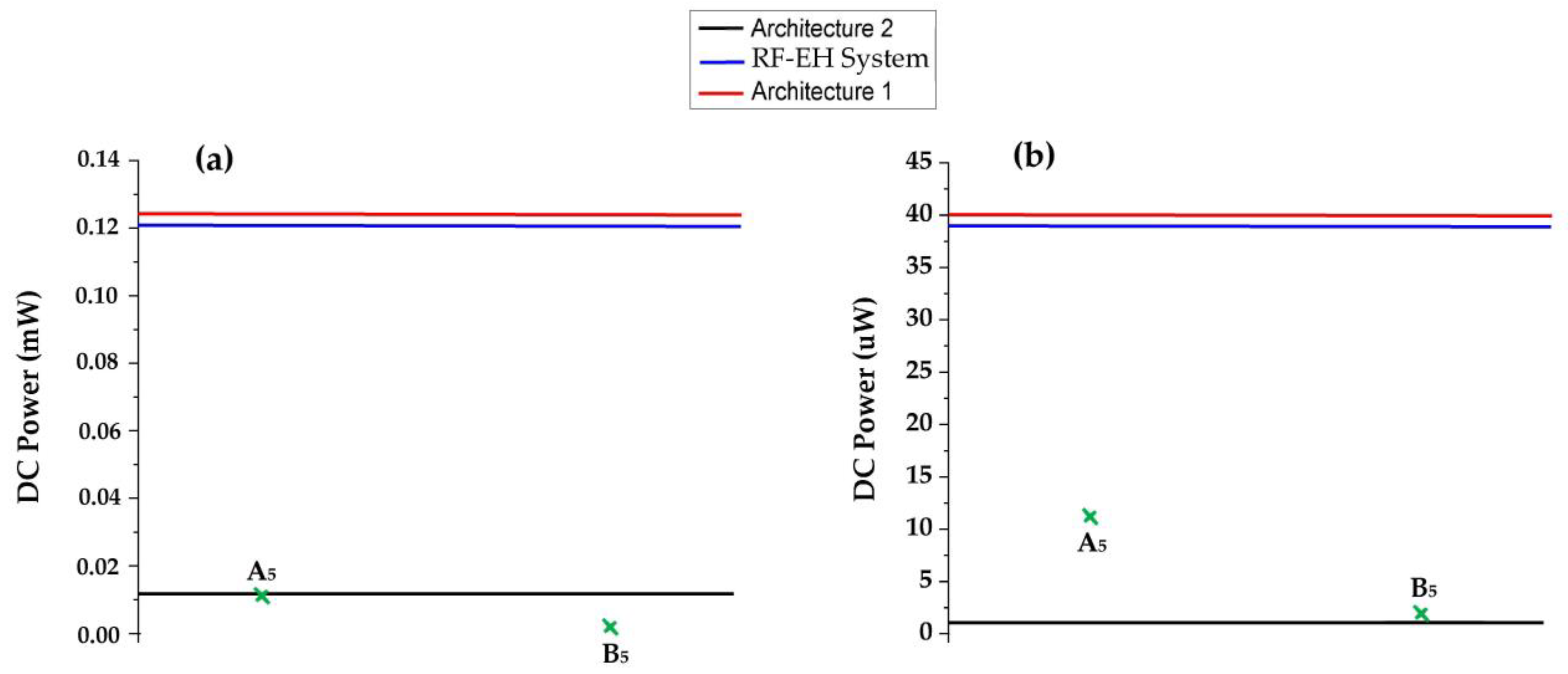
Figure 35.
Feeding ability of the proposed system and architectures at (
a): 110 m, (
b): 122 m from relay antenna compared to minimum required power supply of the temperature sensors. The DC powers A
5 and B
5 correspond to the power supply of sensors reported in the references [
45,
46], respectively.
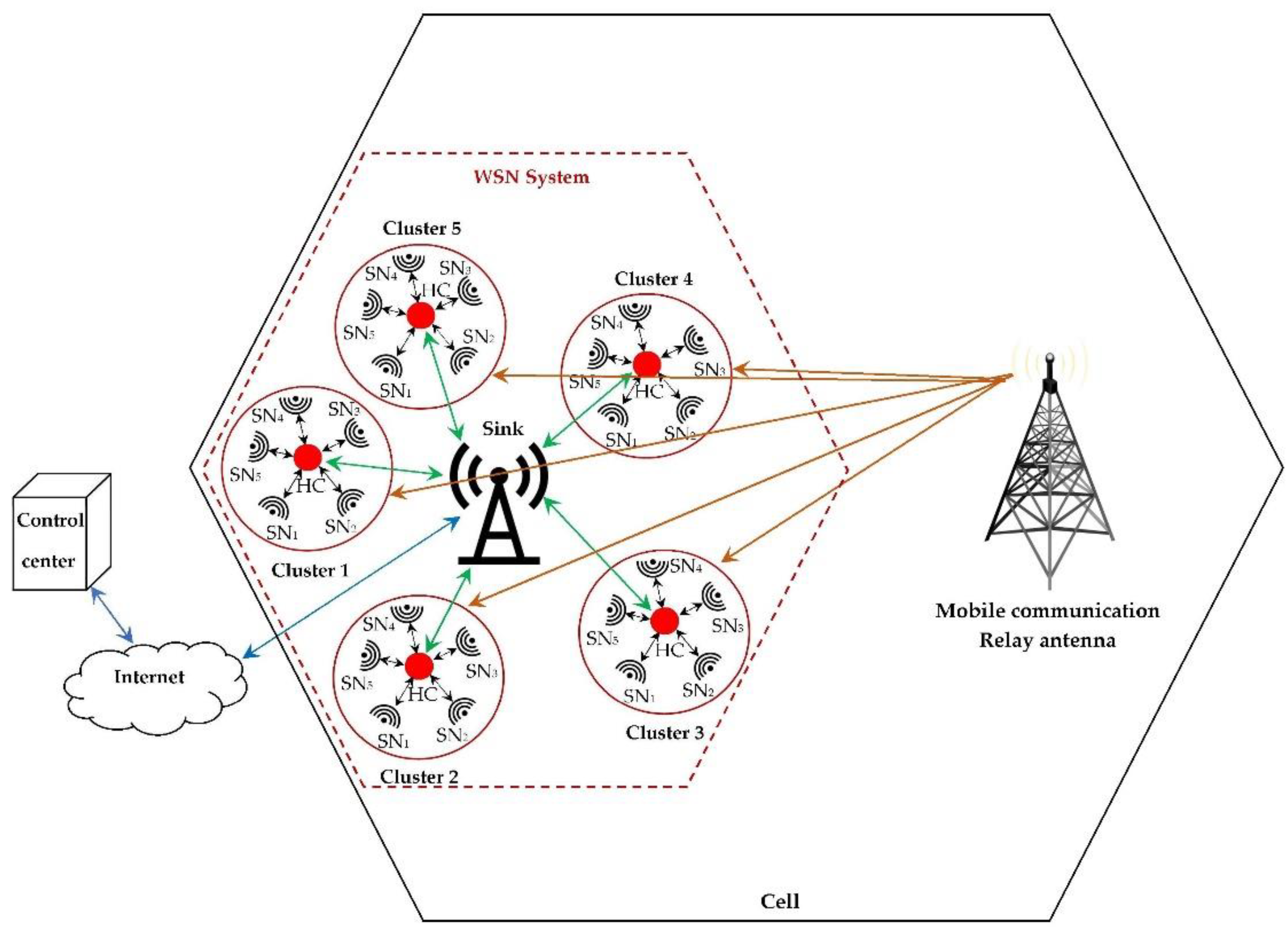
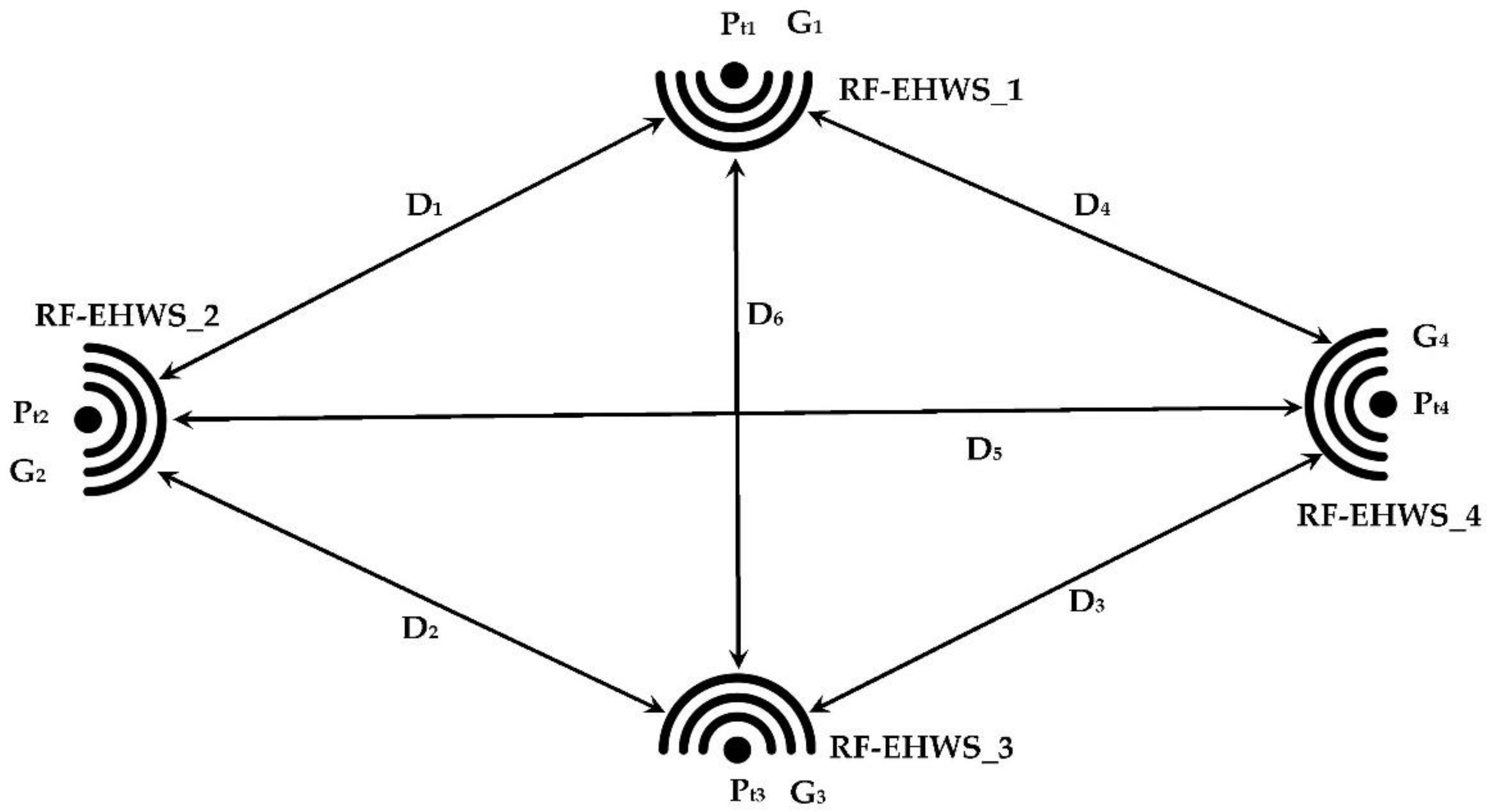
Figure 36.
WSN system architecture within mobile communication cell.
Figure 36.
WSN system architecture within mobile communication cell.
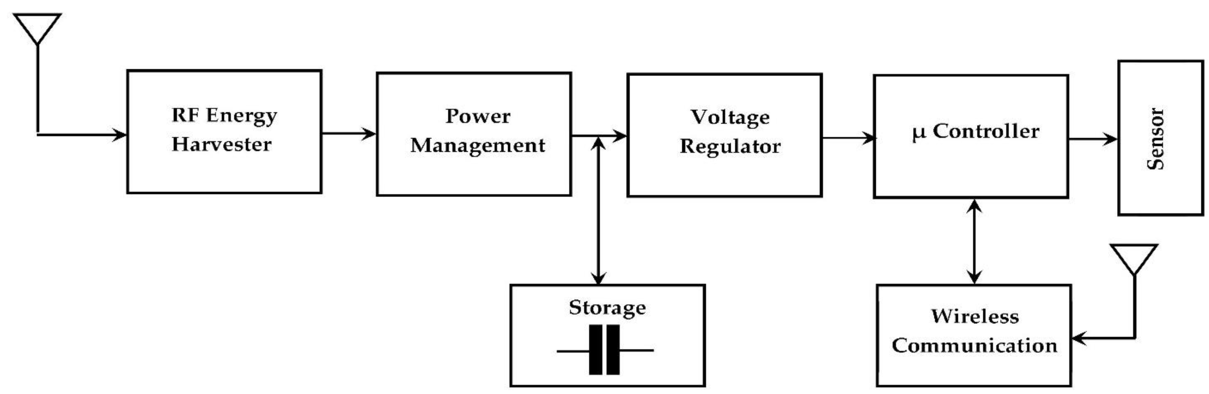
Figure 37.
WSN system architecture for self-powering process.
Figure 37.
WSN system architecture for self-powering process.
Figure 38.
RF-EHWSN system complete architecture.
Figure 38.
RF-EHWSN system complete architecture.
Table 1.
Measured received powers as a function of distance from the mobile communication antenna relay for the three selected networks (GSM-1800, UMTS-2100 and LTE-2.6) in mW.
Table 1.
Measured received powers as a function of distance from the mobile communication antenna relay for the three selected networks (GSM-1800, UMTS-2100 and LTE-2.6) in mW.
| Deff (m) | 22 | 28 | 36 | 45 | 54 | 63 | 72 | 82 | 92 | 102 | 112 | 122 |
|---|
| P(GSM) | 28 | 7.2 | 1.8 | 0.6 | 0.35 | 0.25 | 0.17 | 0.12 | 0.09 | 0.07 | 0.05 | 0.043 |
| P(UMTS) | 18 | 2.8 | 0.8 | 0.35 | 0.22 | 0.17 | 0.13 | 0.097 | 0.08 | 0.05 | 0.032 | 0.028 |
| P(LTE) | 12.8 | 1.8 | 0.6 | 0.25 | 0.16 | 0.1 | 0.08 | 0.07 | 0.05 | 0.036 | 0.018 | 0.015 |
Table 2.
Substrates used in the design of the RF-EH systems.
Table 2.
Substrates used in the design of the RF-EH systems.
| Ref. | [10] | [11] | [12] | [13] | [14] | [15] | [16] | [17] | [18] | [19] | [20] | [21] | [22] | [23] | [24] |
|---|
| Substrates | RT/Duroid 6002 | Flet Polyester/Woven Polyester | FR-4 | Rogers 5880 | Rogers 5880 | FR-4 | Roger 4003C | Rogers RT6002 | Rogers 5880 | Rogers 3210 | FR-4 | Rogers 4003C | FR-4 | Rogers 4003C | Rogers 5880 |
| εr | 2.94 | 1.2/1.5 | 4.4 | 2.2 | 2.2 | 4.4 | 3.55 | 2.94 | 2.2 | 10.2 | 4.4 | 3.38 | 4.4 | 3.38 | 2.2 |
Table 3.
All antenna dimensions.
Table 3.
All antenna dimensions.
| Dimensions | Values (mm) |
|---|
| Lt | 40 |
| Wt | 30 |
| W | 2 |
| La | 3.5 |
| Le | 13.5 |
| L1 | 6 |
| L2 | 6 |
| L3 | 3 |
| L4 | 3.5 |
| L5 | 2 |
| L6 | 2.5 |
| M1 | 1.2 |
| M2 | 2 |
| M3 | 3 |
| M4 | 2 |
| M5 | 7 |
| M6 | 6 |
| M7 | 13 |
| M8 | 12 |
| M9 | 8 |
| W1 | 9 |
| W2 | 9.5 |
| Wg | 5 |
| Lg | 9 |
Table 4.
Electrical ideal element values of the impedance matching circuits for different frequency bands.
Table 4.
Electrical ideal element values of the impedance matching circuits for different frequency bands.
| Frequency | L1 (nH) | L2 (nH) | C1 (pF) | C2 (pF) |
|---|
| 1.8 GHz | 1.5 | 7.9 | 7.5 | 0.55 |
| 2.11 GHz | 1.2 | 3.9 | 9.9 | 1.1 |
| 2.66 GHz | 0.2 | 2.7 | 6.5 | 0.8 |
Table 5.
Values of the parasitic elements of the used inductors and capacitors for the three frequency bands.
Table 5.
Values of the parasitic elements of the used inductors and capacitors for the three frequency bands.
| Frequency | Ls1 (pH) | Ls2 (pH) | CL1 (pF) | CL2 (pF) | RLS1 (mΩ) | RLS2 (mΩ) | RS1 (mΩ) | Rs2 (mΩ) |
|---|
| 1.8 GHz | 0.25 | 7.9 | 1.8 | 0.55 | 60 | 52 | 96 | 82 |
| 2.11 GHz | 0.17 | 5 | 1.98 | 0.6 | 78 | 50 | 80 | 70 |
| 2.66 GHz | 0.1 | 0.1 | 14.8 | 0.5 | 150 | 150 | 5 | 50 |
Table 6.
Output stats of the proposed switch according to the input power levels.
Table 6.
Output stats of the proposed switch according to the input power levels.
| Input Power Levels | Low Input Power | High Input Power |
|---|
| Output 1 | ON | OFF |
| Output 2 | OFF | ON |
Table 7.
Comparison between proposed RF-EH system performances and other systems reported in the literature.
Table 7.
Comparison between proposed RF-EH system performances and other systems reported in the literature.
| References | Input Power (dBm) | Freq. Band (GHz) | Max RF-DC Eff (%) | Maximum Output Voltage (V) | System Dimensions (mm3) | Minimum Load (kΩ) |
|---|
| [10] | 0 | 2.45 | 81 | 1 V at −3.5 dBm | 125 × 80 × 0.25 | 1.4 |
| [11] | −7 | 2.45 | 28.7 | 3 V at −7 dBm | 500 × 64 × 3.3 | 4 |
| [12] | −8 | 0.823–1.337 | 61.7 | 2 V at 0 dBm | 120 × 120 × 0.52 | 10 |
| [13] | 3 | 0.9–3 | 73.4 | 1.2 V at 3 dBm | 200 × 180 × 0.787 | 1 |
| [14] | −1 | 0.45–0.9 | 75 | 1 V at −8 dBm | 160 × 160 × 1.5 | 15 |
| [15] | −10 | 0.91–2.55 | 68 | 0.243 V at −10 dBm | 165 × 125 × 0.8 | 4.7 |
| [16] | −6 | 1.4–2.95 | 27.5 | 0.484 V at −6 dBm | 100 × 80 × 0.87 | 0.8 |
| [17] | −3 | 1.7–1.8 and 2.1–2.7 | 67 | 1.1 V at −3 dBm | 145 × 145 × 1.53 | 2 |
| [18] | −5 | 0.866, 0.925 and 2.45 | 65 | 0.7 V Ambient | 115 × 71 × 0.787 | 10 |
| [19] | 0 | 2.45 and 5.8 | 58 | NA | 64 × 64 × 1.24 | 0.7 |
| [20] | −27 | 0.95, 1.74, 2.12, 2.42 and 2.90 | 66.5 | 0.797 V Ambient | 220 × 220 × 30 | 2.11 |
| [21] | −10 | 1.8 | 51.3 | 0.129 V Ambient | 100 × 100 × 60 | 6 |
| [22] | −3 | 2.45 | 45.3 | 0.782 V Ambient | 337 × 226 × 10 | 3 |
| [23] | 10 | 5.8 | 68 | 1.1 V at 10 dBm | 86 × 24 × 0.813 | 0.22 |
| [24] | 6.5 | 5.2 and 5.8 | 54.9 | 0.7 V at 6.5 dBm | 87 × 90.9 × 0.787 | 0.2 |
| [25] | 5.8 | 0.9, 1.8, 2.1 and 2.45 | 84 | 0.9 V at −15 dBm | 100 × 100 × NA | 11 |
| This Work | 10 | 1.8, 2.1 and 2.66 | 71.5% | 3.1 V Ambient | 65 × 64 × 0.67 | 2 |


 Measurement,
  Simulation
  Co-simulation with parasitic elements.


