1. Introduction
Elliptic curve cryptography (ECC) is an asymmetric cryptographic approach proposed independently in 1985 by Neal Koblitz [
1] and Victor S. Miller [
2]. Elliptic curves are used in various fields of application. Many interesting details about ECC including its genesis can be found in [
3]. The advantage of ECC in comparison to RSA [
4] is the possibility to use significantly shorter keys than RSA by maintaining the same security strength. ECC is used to share secret keys, for signing messages and for authentication, which are essential when it comes to communication, e.g., in the fields of the Internet of Things and wearable sensors [
5]. The main operation of ECC is the elliptic curve point multiplication
kP, where
P is a point of an elliptic curve (EC), and
k is a scalar, also denoted as
key. The length of the scalar depends on the type of EC used and on the security requirements. Currently, keys have to be about 200–300-bit long. There are two types of ECs standardized for use in cryptographic protocols: ECs over extended binary fields
GF(2
n), and ECs over prime fields
GF(
p). The
kP operation is the most time- and energy-consuming operation in ECC protocols. The Montgomery
kP algorithm (the
Montgomery ladder) using Lopez–Dahab projective coordinates [
6] is the algorithm most often used in hardware implementations for accelerating cryptographic operations for ECs over extended binary fields
GF(2
n) due to its fast execution time. It requires only six field multiplications for processing a key bit, whereby all other operations—field additions and squaring operations as well as register operations—can be implemented in parallel to field multiplications. For ECs over
GF(
p), no comparably fast algorithm is known. Usually, many more field multiplications have to be calculated. Additionally, mathematical operations—multiplications, additions and subtractions in prime fields—implemented in hardware are significantly slower than the mathematical operations in extended binary fields due to the delay caused by the carry bit propagation. For large networks or time-critical applications, a fast execution of cryptographic operations is essential. For automotive applications, at least 1000 signature verifications per second are required; in big cities, this number even reaches up to 4000. Corresponding to the Elliptic Curve Digital Signature Algorithm (ECDSA) [
7], only one
kP operation has to be calculated for a generation of a digital signature, but two
kP operations have to be calculated for its verification. To fulfil the speed requirements, efficient methods have to be applied at each implementation level, i.e., field operations,
kP operation and ECDSA acceleration. For example, the Straus–Shamir trick [
8,
9] is a well-known means to accelerate the signature verification for ECs over
GF(
p).
An additional requirement for applications that are sensitive to manipulations is that the implemented algorithms have to be resistant to side-channel analysis (SCA) attacks, if an attacker has physical access to the working cryptographic device. The goal of attackers is to reveal the scalar
k processed during a
kP execution. Many
kP algorithms process the scalar
k bitwise, i.e.,
bit-by-bit. The Montgomery
kP algorithm for ECs over
GF(2
n) is known in the literature to be resistant against simple SCA attacks due to its regularity [
10,
11], i.e., the sequence of operations for the processing of the bit value “0” of the scalar
k is the same as for the processing of the bit value “1”. Due to the fact that a point doubling and a point addition have to be calculated for processing each key bit in the main loop of the Montgomery ladder, the Montgomery
kP algorithm can be considered a type of a
double-and-add-always algorithm. In order to reduce the execution time of cryptographic operations,
kP algorithms for ECs over
GF(
p) are often based on the binary
double-and-add algorithm. In that case, the processing of the key bit “0” requires only a single point doubling calculation, but the processing of the key bit “1” requires two point operations—a point doubling and a point addition. The sequence of mathematical operations for a point doubling differs from that of a point addition. This results in a different energy consumption for each type of point operation, i.e., the power profile of a point doubling is distinguishable from the power profile of a point addition. If an attacker can measure the current drawn by the device or its electromagnetic emanation during a
kP execution (hereafter
kP trace), and the differences are observable by a visual inspection of the trace, the implementation is vulnerable to simple SCA attacks. To make the
double-and-add algorithm resistant to simple SCA attacks, the sequence of the field operations for an EC point doubling has to be the same as the sequence of the field operations for an EC point addition: for example, using a unified point addition formula. Another strategy is the implementation of both point operations using a repeated (short) sequence of field operations. For example, a point doubling can be implemented as a sequence repeated 16 times containing “two additions, one additive inverse, one multiplication and four write-to-register operations”, and a point addition can be implemented as a sequence of the same operations repeated 10 times. This strategy was proposed in [
12] and is known as the “atomicity” principle because the short operation sequence is denoted as an “atom”. In [
13], longer atomic patterns were proposed for EC point doubling and addition, using special mixed Jacobian–affine coordinates. The point doubling as well as the point addition requires only 10 field multiplications, 10 field additions/subtractions and 21 write-to-register operations, i.e., this algorithm is also the fastest one (see Section 4 in [
13]).
This paper is an extended version of the paper entitled “Fast Dual-Field ECDSA Accelerator with Increased Resistance against Horizontal SCA Attacks” presented in 2021 at the IEEE International Conference on Cyber Security and Resilience (CSR) [
14]. We implemented an elliptic curve point multiplication for the following four NIST elliptic curves [
7]:
B-233,
B-283,
P-224 and
P-256, in hardware to accelerate the generation and verification of digital signatures. The following contributions are described in [
14] and here:
Applying the four-segment iterative Karatsuba multiplication formula (MF) to both types of Galois fields. The multiplication formula was proposed and efficiently applied in [
15] for accelerating the field multiplication in
GF(2
n). To the best of our knowledge, we are the first team to apply this formula to implement a dual-field multiplier. In comparison to the classical multiplication formula, the segmentation of multiplicands in four parts, the four-segment Karatsuba MF, is much faster: the product can be calculated in only nine clock cycles, which is seven clock cycles less than when applying the classical MF. It reduces the calculation time as well as the energy consumption of
kP executions for ECs over
GF(
p) by about 40%. Thus, the automotive requirement to be able to perform 1000 signature verifications per second can be reached even with non-scaled technologies: for example, using a 250 nm gate library [
16].
Evaluation of the resistance of the implemented four-EC design against horizontal
address-bit differential power analysis (DPA) attacks using the
comparison to the mean method [
17]. Analyzing a
kP power trace simulated for EC
B-233 in the four-elliptic-curve design, we obtained only the two best key candidates with a correctness of about 87% and 85%, respectively. In comparison to this, attacking the single
B-233 curve
kP design resulted in six key candidates being obtained, with a correctness higher than 95%—so the resistance of the four-elliptic-curve design is significantly better than that of the single designs.
Verification of our assumption about the vulnerability of the atomic pattern algorithm [
13] to horizontal SCA attacks. Analyzing power traces for EC
P-224, we obtained four key candidates with a correctness of 97% or higher. Attacking EC
P-256, we were able to reveal the key completely, i.e., three key candidates had a correctness of 100%.
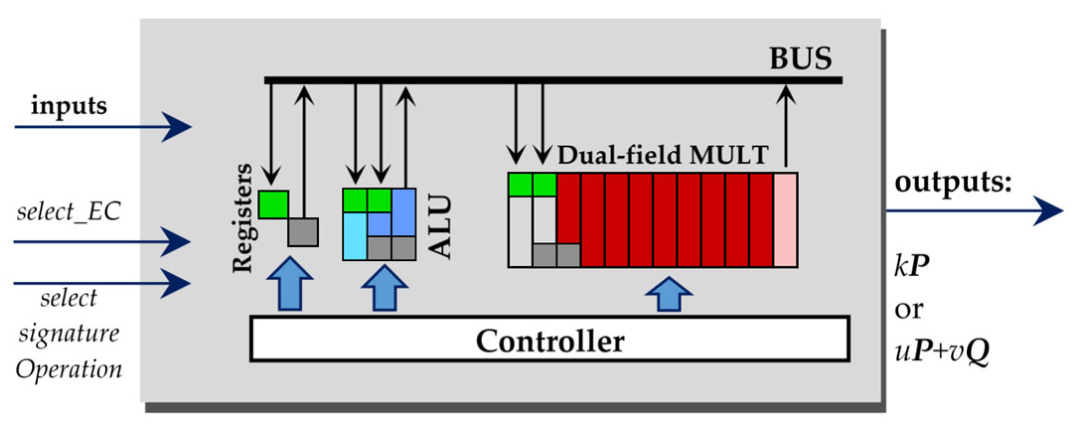
For our implementation, we selected
kP algorithms that are fast and mentioned in the literature as resistant against simple SCA attacks, due to the regularity and atomicity principles of the algorithms. More specifically, we selected the Montgomery ladder using projective Lopez–Dahab coordinates [
6] for ECs over
GF(2
n), and the atomic pattern algorithm using mixed Jacobian–affine coordinates [
13] for ECs over
GF(
p).
The vulnerability of the Montgomery ladder to horizontal address-bit DPA attacks is known [
18]. The key-dependent addressing of registers or other blocks is “visible” even through simple statistical analysis of a single
kP trace. The resistance of the atomic pattern algorithm [
13] against horizontal address-bit DPA attacks has, to the best of our knowledge, not been evaluated yet. We assumed that the power profiles of point doublings and point additions, implemented corresponding to the atomic patterns described in [
13], are distinguishable due to the key-dependent use of registers in these patterns. Thus, the algorithm [
13] is, theoretically, vulnerable to horizontal address-bit DPA attacks, too. However, we expected that the resistance of our design for four ECs will be higher than that of a design for a single EC, due to the fact that some operations (for example, field reductions) are always performed for all four ECs in our design. This increases the energy consumption of the
kP design, but it is a type of noise that can hide the key-dependent addressing of the registers. Our assumptions were confirmed.
Additionally, we extended our conference paper [
14] with the following investigations:
We extended the evaluation of our design’s resistance against horizontal DPA attacks. We ported the design to an FPGA, captured electromagnetic traces of the kP execution, repeated our attack analyzing the measured traces and compared the attack results with those obtained by attacking the simulated traces of an ASIC. Despite the significant differences between the target platforms—a cryptographic ASIC in the IHP 250 nm technology and an FPGA in the 28 nm technology—the resistance of the cryptographic designs against horizontal DPA attacks is quite similar, i.e., the performed attack was successful.
We performed additional investigations by applying an automated simple analysis attack against the measured electromagnetic traces for the ECs
P-224 and
P-256. We discovered and demonstrated that the atomic patterns presented in [
13] are vulnerable to simple analysis attacks.
We proposed an approach to reduce the success of simple analysis attacks, as well as horizontal attacks, and evaluated its effectiveness by attacking the electromagnetic traces of the modified design.
The rest of this paper is structured as follows. In
Section 2, we focus on the implementation details of our unified design. The results of the horizontal DPA attacks performed against simulated power traces are presented and discussed in
Section 3.
Section 4 provides the results of a horizontal differential electromagnetic analysis performed against electromagnetic traces measured on an FPGA. In
Section 5, we present the results of our automated simple analysis attack. An approach focused on reducing the success of horizontal attacks is presented and evaluated in
Section 6. This paper ends with short conclusions.
3. Horizontal DPA Attack: Analysis of Simulated Traces
3.1. Power Trace Simulation
We synthesized our ECDSA accelerator for the IHP 250 nm technology. We used the Very High Speed Integrated Circuit Hardware Description Language (VHDL) for the behavioral modeling of our design and synthesized it using the Synopsys Design Compiler Version K-2015.06-SP2. The maximum achieved clock frequency was 62.5 MHz (16 ns clock cycle period) after synthesis. For each of the four ECs, we generated power traces of a
kP execution using Synopsys PrimePower Version Q-2019.12-SP1. The PrimePower tool uses the gate-level simulation activity stored in the activity file to estimate the averaged power consumption of the design. It can also precisely analyze the power consumption of the design for each clock cycle within a given time interval, i.e., it allows simulating a power trace of
kP executions, with the given inputs. Power traces were simulated with a step of 0.01 ns, i.e., our trace contains 1600 simulated values per clock cycle. We do not need such a fine-grained simulation for the experiments described in this work. To simplify the analysis, and due to the fact that the simulated trace is noiseless, we performed a trace compression. For each clock cycle, we calculated the sum of its sampling values and represented it using this single value (i.e., the
y-axis shows the average power consumption in W, multiplied by 1600).
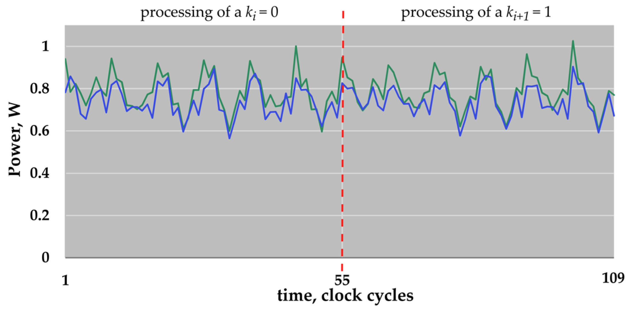
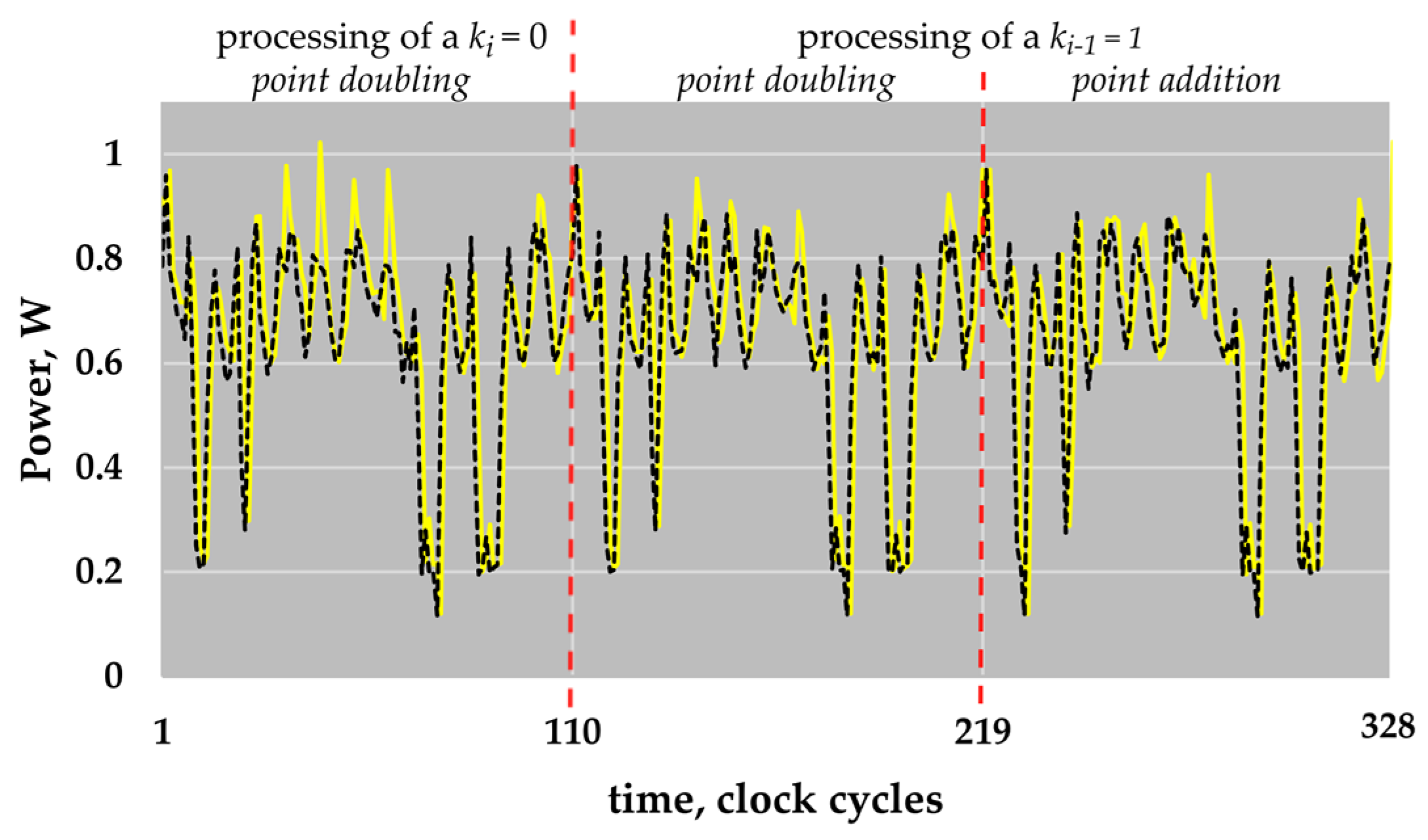
Figure 4 shows parts of the compressed power traces simulated for the ECs
B-233 and
B-283. The parts shown correspond to the processing of two key bits, i.e., “01”.
Figure 5 shows parts of the compressed power traces simulated for the ECs
P-224 and
P-256. The shown parts also correspond to the processing of two key bits “01”, i.e., here, three atomic patterns are shown: two point doublings, and a point addition.
The clock cycles with reduced energy consumption are easy to see in
Figure 5. As described above, the non-active field multiplier is the reason for the reduced energy consumption. These clock cycles are a type of marker. They “show” the periodicity of an atomic pattern. The knowledge about the period of atomic patterns is helpful for the preparation of different attacks. In comparison to the atomic patterns for the point operations in
GF(
p), the atomic patterns corresponding to the processing of a key bit in
GF(2
n) do not have such a type of marker in our implementation.
Please note that all traces shown in
Figure 4 and
Figure 5 are already compressed power traces, i.e., the row traces—the simulated power traces—were already partially prepared for the analysis.
3.2. Horizontal Power Analysis Attack
In this paper, we concentrated on single-trace attacks that are also known as horizontal attacks. In our horizontal attacks, we did not exploit any key-dependent correlations based on the processing of the same/different data as in horizontal correlation analysis attacks [
21], or the storing of data in registers as in template attacks [
22]. Our attack did not exploit the key-dependent data flow. The attack was based on the assumption that key-dependent addressing of different registers or other blocks of a cryptographic design is distinguishable. This assumption was exploited in [
23] in 2002 for revealing a key using 1000
kP traces, i.e., it was a successful vertical attack. Since 2017, successful horizontal attacks exploiting key-dependent addressing of the Montgomery ladder for ECs over
GF(2
n) have been reported [
18]. In detail, the following points were assumed as the basis of these attacks:
The attacked design processes a secret binary number k = kn−1kn−2…k1k0 bitwise;
The addressing of the design blocks for processing the key bit value “0” differs from the addressing of the design blocks for processing the key bit value “1”;
The key-dependent addressing of the design blocks makes the shapes of the processing of the key bit value “0” distinguishable from the shapes of the processing of the key bit value “1”;
The differences in the shapes can be detected using statistical analysis methods or unsupervised machine learning algorithms.
Simple SCA attacks are successful if the power profiles of “0” key bits differ significantly from the power profiles of “1” key bits. These strong differences are often caused by the different sequences of mathematical operations in the main loop of the
kP algorithm during the processing of “0” and “1” key bit values. These differences can be detected by visual inspection of the simulated or measured traces. Designs with the same sequence of operations for the processing of different key bit values—regular designs—are considered as resistant against simple SCA attacks. The differences caused by the key-dependent addressing of blocks are no longer significant, but they can still be “seen” using statistical analysis as a type of “magnifying glass”. Here, we performed an analysis using the
comparison to the mean approach corresponding to [
17].
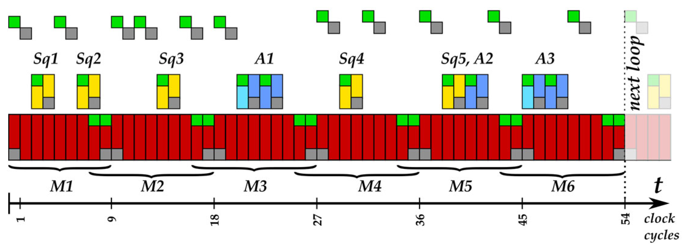
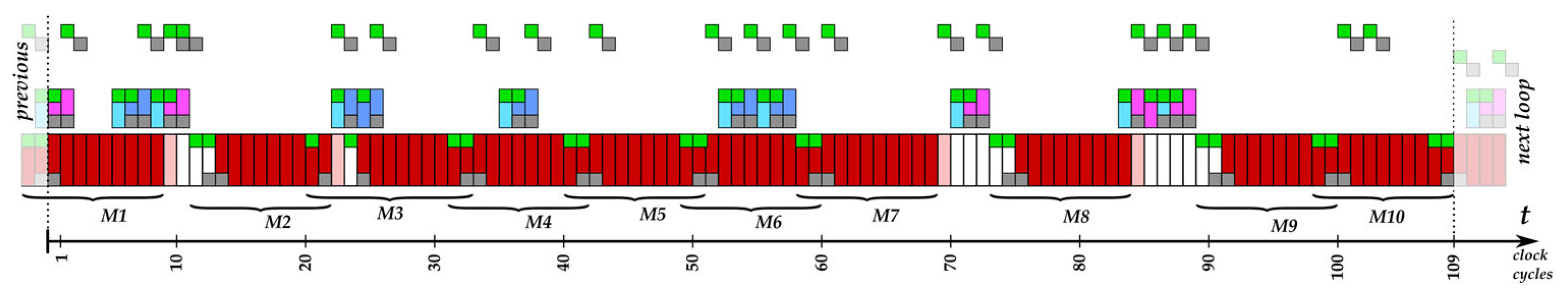
In this work, we have two types of atomic patterns:
Due to the duration of an atomic pattern (in clock cycles) and the compression of the power trace (only a single value represents each clock cycle), the power profile of an atomic pattern consists of:
We denote the current sample in an atomic pattern power profile (hereafter atomic profile) using the letter j in this work. Thus, for an atomic pattern:
For ECs over GF(p), j ∈ {1, 2, …, 109};
For ECs over GF(2n), j ∈ {1, 2, …, 54}.
We numbered each power profile of the processing of key bit ki in the main loop of the implemented algorithm using the same index letter i. Please note that in the main loop in our implementation for ECs over GF(2n), the key bits kl−3, kl−4,…, k1, k0 are processed, i.e., i∈{l−3, l−2,…, 1,0}, and for ECs over GF(p), i∈{l−2, l−1,…, 1,0}.
For the simulated, compressed kP traces of ECs B-233 and B-283, we:
Calculated the mean atomic profile averaging all atomic profiles.
Compared the value of the sample number 1 in the mean atomic profile with the sample number 1 in the ith atomic pattern profile, for all i in the analyzed trace:
- ⚬
If the value of the sample number 1 in the ith atomic pattern profile was higher or equal to that in the mean atomic profile, we assumed that the key bit value ki = “1” was processed; otherwise, we assumed that the key bit value ki = “0” was processed.
- ⚬
Therefore, we made an assumption about all l−2 bits of key candidate 1, i.e., we extracted key_candidate_1.
Repeated the comparison for each of the remaining j sample numbers in order to extract the corresponding key_candidate_j.
Evaluated the correctness of the extracted key candidates, i.e., we compared each key_candidate_j with the scalar k processed in the analyzed kP execution. The result of the comparison is the relative number of correctly revealed key bits. For example, if 200 bits of a key candidate were revealed correctly and the scalar k processed was 233-bit long, the correctness δ = (200/233)⸱100% ≈ 85.8%.
We analyzed the kP traces for ECs P-224 and P-256 in a similar way. We calculated the mean power profile of point operations performed in the main loop of the kP executions for ECs P-224 and P-256. The mean profile contains 109 samples—one sample per clock cycle. We compared the mean profile of the point operation calculated for a kP execution with each point operation profile in the kP execution trace sample-wise. Using the mean atomic profile, we made an assumption about the point operations, i.e., we distinguished point additions and point doublings. Each point doubling profile followed by a point addition profile was denoted as a processed key bit value of “1”, corresponding to the implemented double-and-add algorithm. For the evaluation of each extracted key candidate, we calculated its correctness as described above.
Thus, for each kP trace analyzed for ECs over GF(p), we extracted 109 key candidates, and for ECs over GF(2n), we extracted 54 key candidates.
Please note that if the correctness of a key candidate is less than 50%, it means that our assumption about the processed key bit value was wrong. Bitwise inversion of the key candidate gives us the key candidate, for which the correctness is (100% − δ) > 50%.
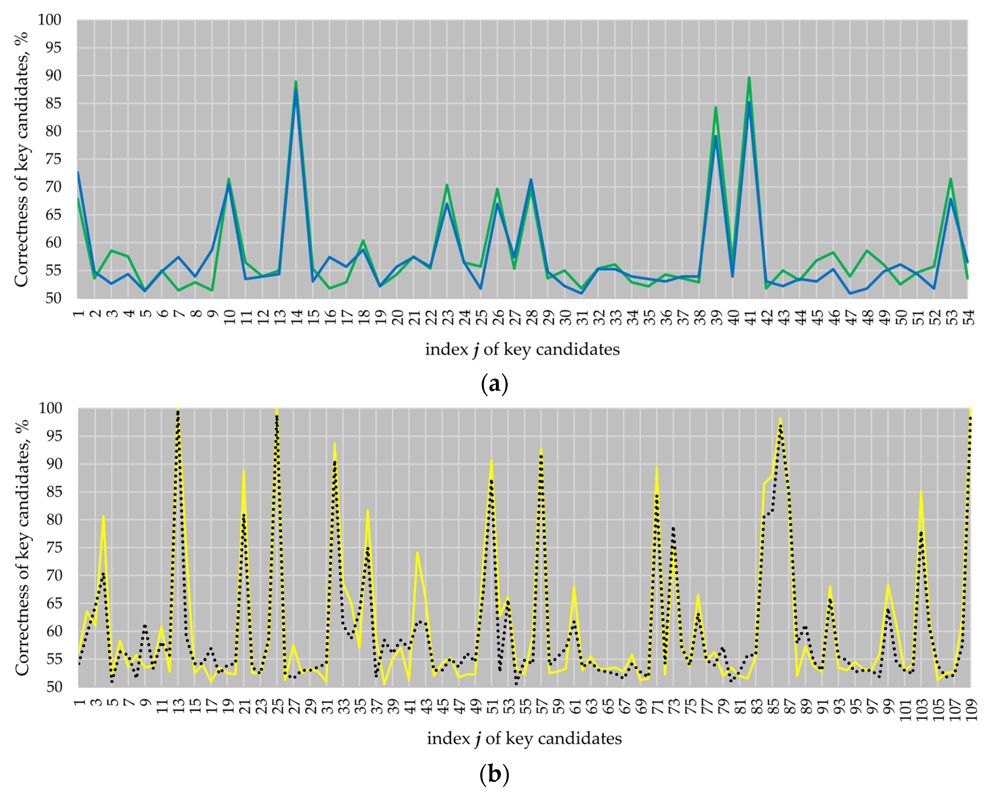
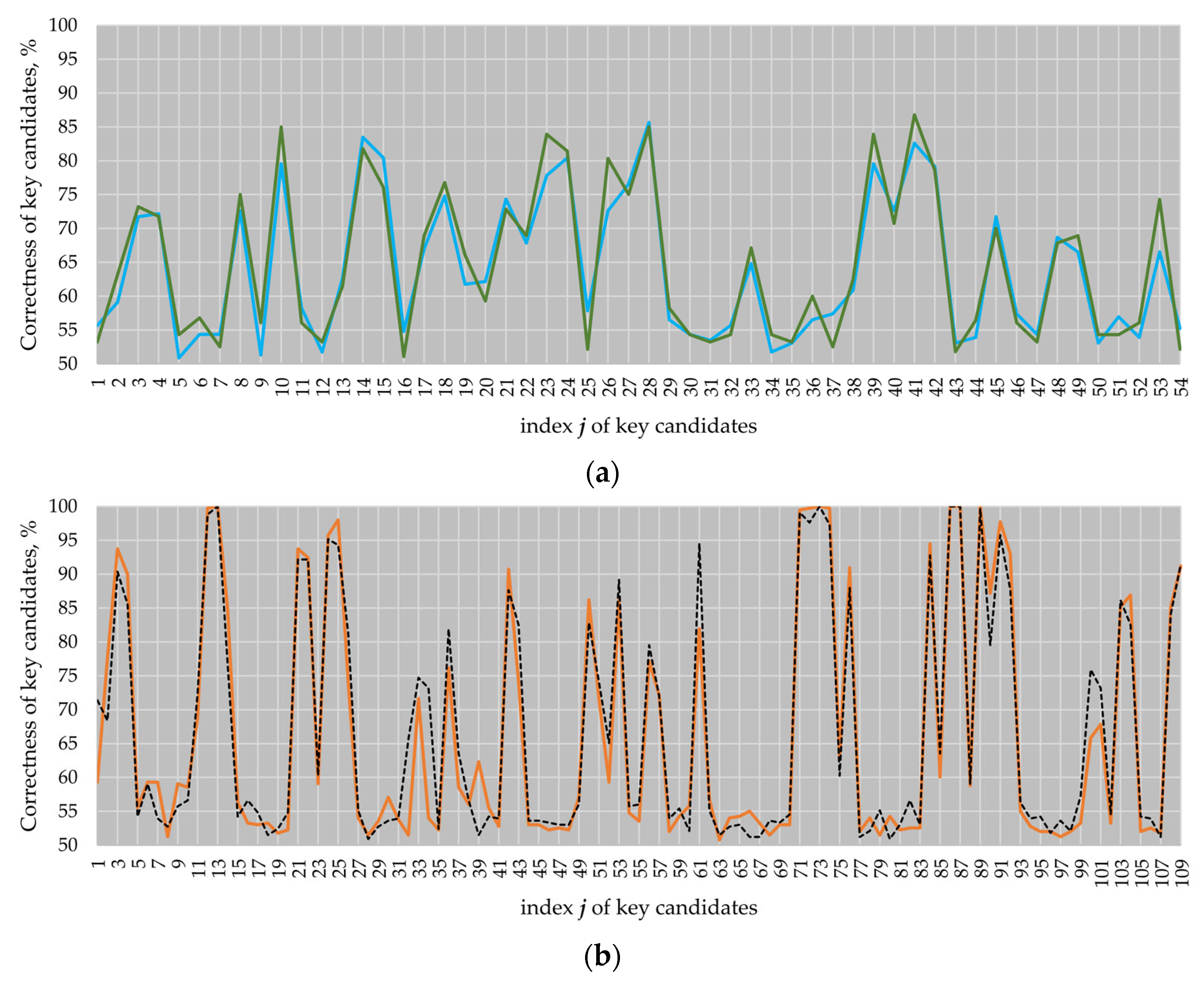
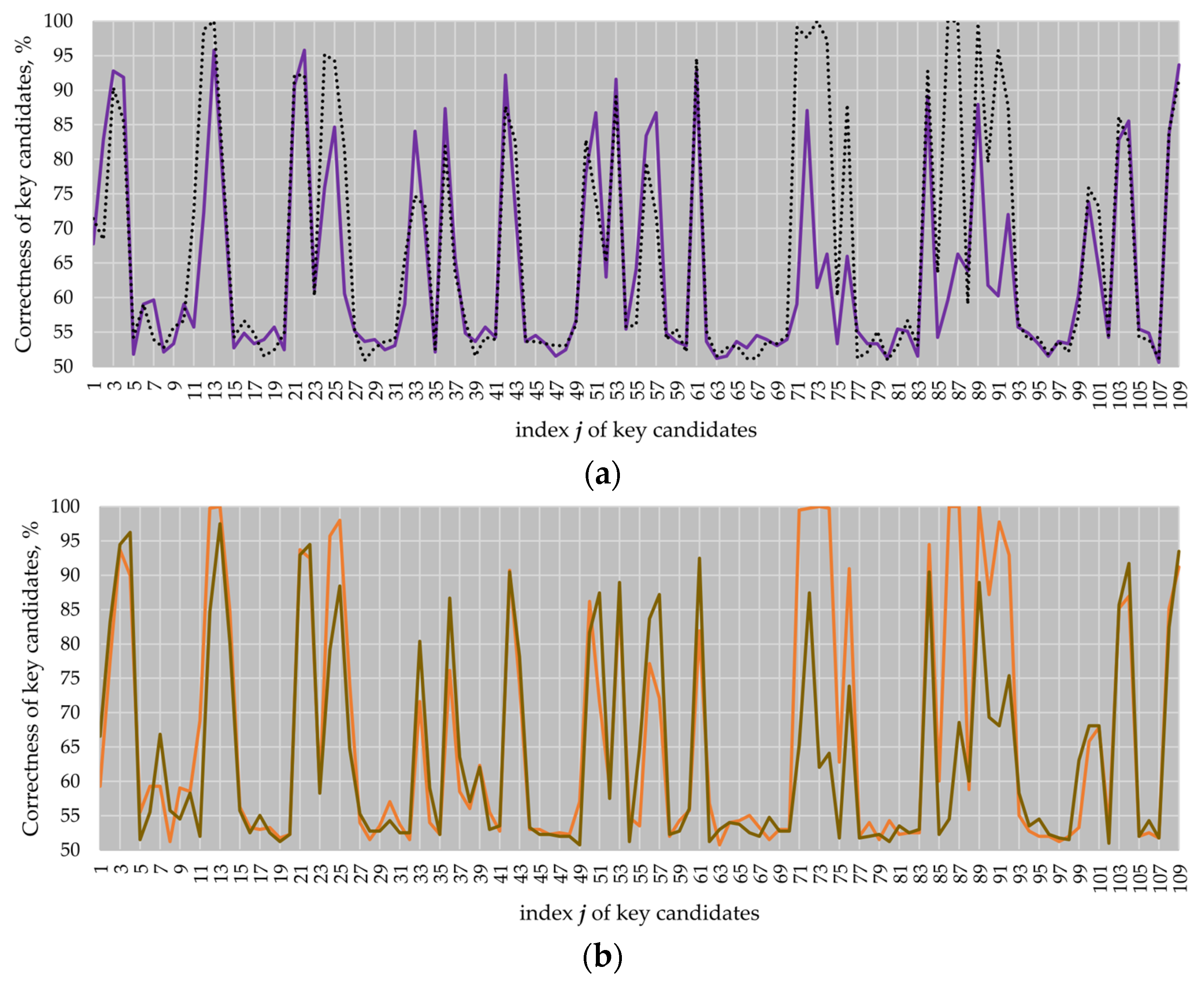
Figure 6a shows the attack results for the ECs
B-233 and
B-283, and
Figure 6b shows the attack results for the ECs
P-224 and
P-256.
The results of our attacks demonstrate that the atomicity patterns do not prevent horizontal attacks from being successful. On attacking EC
P-224, we obtained four key candidates with a correctness higher than 97% (see key candidates 13, 25, 86 and 109). On attacking EC
P-256, we fully revealed the key (see key candidates 13, 25 and 109 with a correctness of 100%). Well-known randomization techniques such as secret scalar randomization, randomization of the projective EC point coordinates or EC point blinding [
24] are effective against vertical attacks, i.e., if key-dependent data processing is exploited to extract the key. However, they are not effective [
25,
26] against attacks exploiting the key-dependent addressing of the design blocks, i.e., their application when using atomic patterns does not prevent horizontal attacks that exploit the addressing from being successful. In other words, they do not prevent simple SCA attacks that are looking for highly fine-grained differences in the trace. The weak point of the atomicity principle is the assumption that the addressing of different registers (or other blocks of the design) is indistinguishable. The same weak point cryptographic designs have when implementing the regularity principle as a countermeasure against simple SCA attacks. This does not hold true if the design is a hardware implementation. Therefore, approaches for hiding the addressing have to be applied in addition. One of the well-known approaches is adding noise. The activity of design blocks is a type of noise.
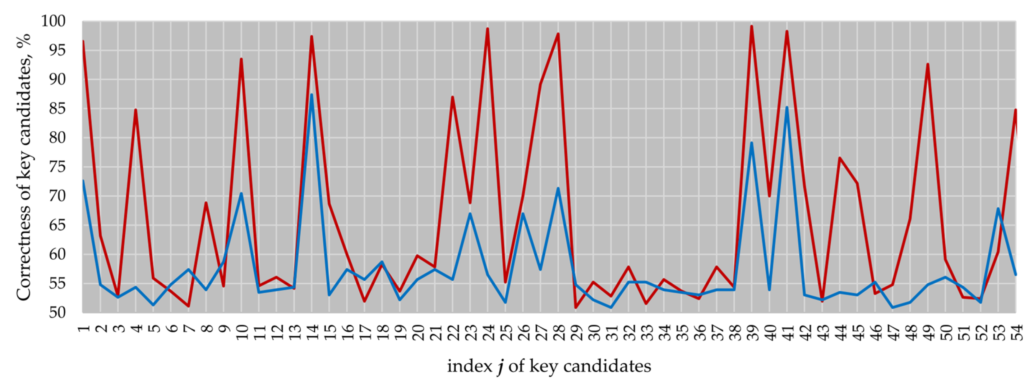
Figure 7 demonstrates how the activity of the blocks in our four-curve design decreased the success of the same attack performed analyzing a
kP trace recorded when only the EC
B-233 kP design was active. In the case of the single EC
B-233 kP design, we obtained 12 key candidates with a correctness higher than 85%, whereby 6 of the 12 key candidates had a correctness higher than 95% (see red line in
Figure 7). In the case of the four-active-EC design, only two key candidates had a correctness of about 85%, whereby the correctness of the best key candidate was 87% (see blue line in
Figure 7).
4. Horizontal DPA Attack: Evaluation of an FPGA Implementation
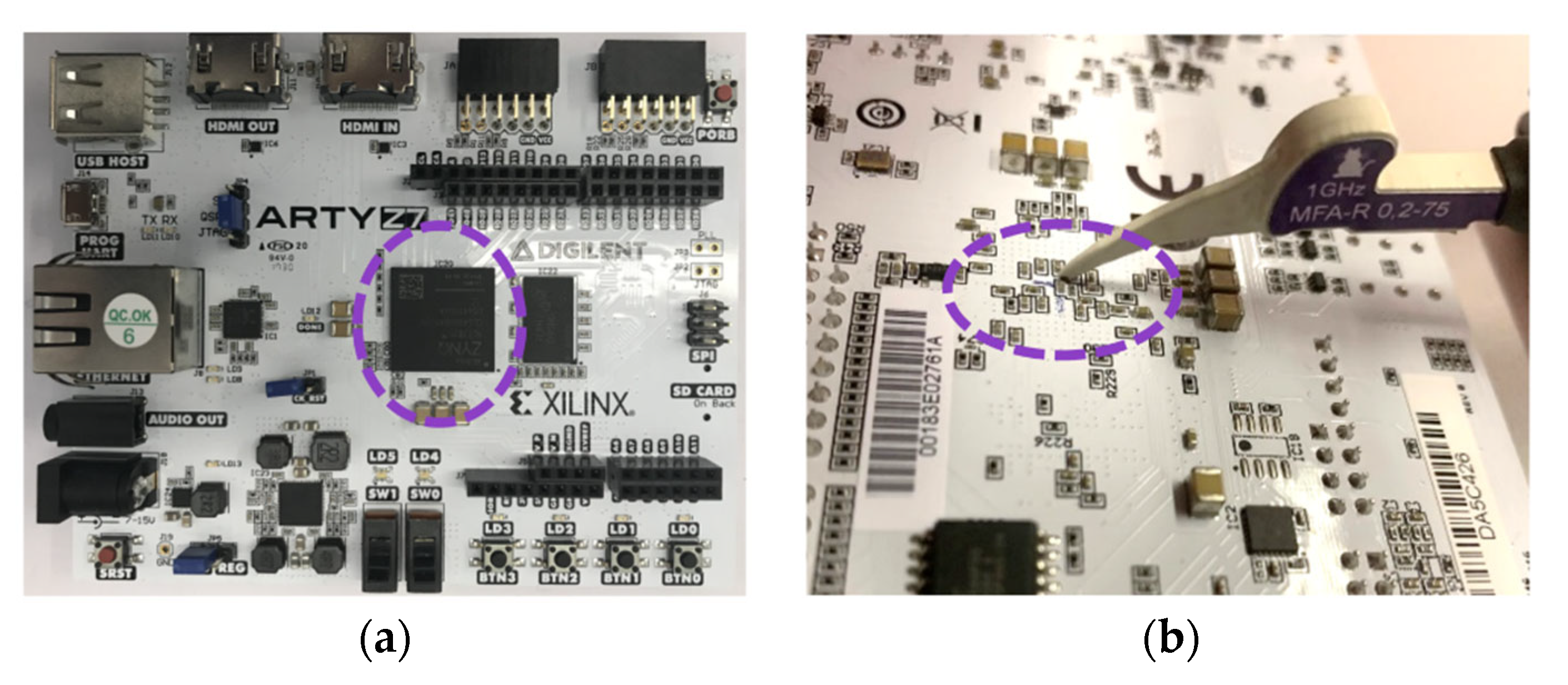
We ported our design to an FPGA with the goal to confirm the conducted investigations on a real device. As the target platform, we took an Arty Z7-20 development board (
Figure 8a) equipped with a Xilinx 7-series FPGA produced in a 28 nm technology. The attacked FPGA is marked with a circle in
Figure 8.
Table 3 shows the FPGA resources used by the whole design as well as its multiplier block.
The maximum operating frequency for the design is slightly above 25 MHz. However, we applied a clock frequency of 10 MHz to increase the number of captured samples per clock cycle during the collection of kP traces.
The board used is not suitable for the connection of a current probe. Therefore, instead of measuring the power traces that require a board modification, we applied a near-field magnetic probe to capture electromagnetic traces. The electromagnetic traces were captured during the execution of
kP operations at a 10 GS/s sampling rate by a LeCroy WavePro 254HD oscilloscope and a Langer MFA-R 0.2-75 [
27] near-field probe connected to it. We placed the MFA-R probe close to one of the power decoupling capacitors. The exact location of the probe is shown in
Figure 8b.
We repeated our
comparison to the mean attack against measured traces of the
kP execution as described in
Section 3. All the design inputs for the
kP operations, i.e., coordinates of the EC points as well as scalars for each of the curves, were kept the same as those used during the simulations of the power traces.
Figure 9a shows the attack results for the ECs
B-233 and
B-283, and
Figure 9b shows the attack results for the ECs
P-224 and
P-256.
On attacking EC P-224, we obtained four key candidates with a correctness of 100%, i.e., we fully revealed the key (see key candidates 13, 73, 86 and 87). On attacking EC P-256, we obtained five key candidates (clock cycles 13, 73, 86, 87 and 89) that are identical to the processed key.
Table 4 summarizes the results of the
comparison to the mean attack performed against the simulated power traces and measured electromagnetic traces of the
kP executions for the four investigated curves.
As it can be seen from
Table 4, despite the significant difference between the target platforms used for the simulation and measurements of the traces (i.e., ASIC and FPGA), the results are quite similar. For the binary elliptic curves investigated here, there were no key candidates revealed with a correctness of more than 90% using the traces simulated for the ASIC as well as using the traces measured on the FPGA. In contrast to this, for the investigated elliptic curves over prime fields, the results obtained using the measured traces are far worse than for the simulated traces. The number of key candidates extracted with a correctness of more than 90% increased from 6 and 7 for ECs
P-224 and
P-256, respectively, to 18 and 20.
5. Automated Simple Analysis Attack
We decided to investigate our design further by analyzing the uncompressed measured traces of the elliptic curves P-224 and P-256. Analysis of uncompressed traces can provide advantages to designers for determining the leakage sources as well as attackers when revealing the key. If the leakage source is not very high/strong, or if the leakage duration is short in comparison to that of the clock cycle, the compression can “hide” this leakage, at least partially.
The main purpose of the atomicity principle is to protect elliptic curve scalar multiplication against simple side-channel analysis attacks. Therefore, we applied an automated simple analysis attack against measured traces as described in [
28], i.e., we tried to distinguish the point doubling atomic pattern from that of the point addition using our software that helps to detect tiny differences in a similar way to a magnifying glass.
As already mentioned before, the design was run at a 10 MHz clock frequency, and the traces were captured by an oscilloscope at a 10 GS/s sampling rate. These parameters resulted in 1000 measured samples per clock cycle. Hence, a single atomic pattern, consisting of 109 clock cycles in our implementation, is represented by 109,000 values within the measured trace.
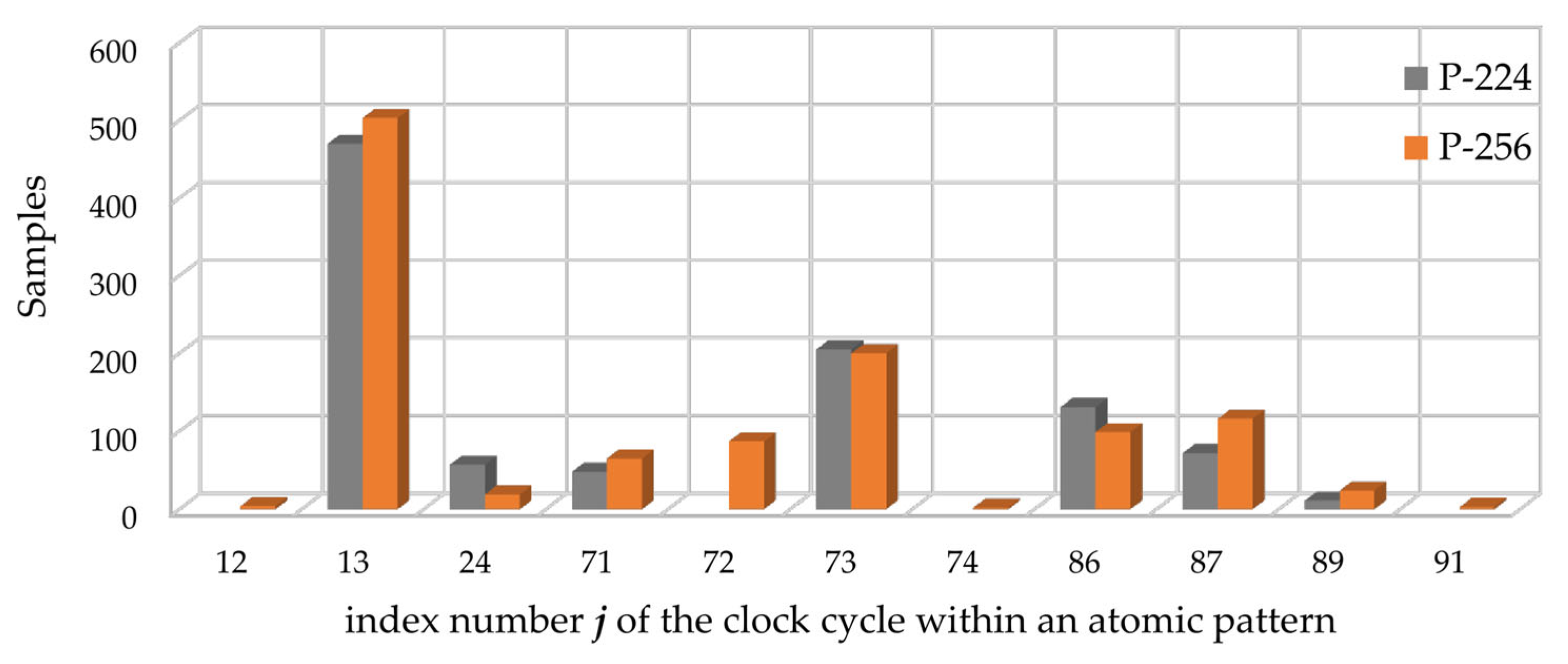
In total, for each of the traces, out of 109,000 samples in the atomic pattern, we identified 994 samples for EC
P-224 and 1122 samples for EC
P-256 that allow for successfully revealing the processed scalar using simple visual inspection. Detailed information about the distribution of such samples within the atomic pattern as well as visualization of such data is presented in
Table 5 and
Figure 10.
Taking into account the information presented in
Figure 3 and
Figure 10, it is obvious that all the significant leakage comes from the clock cycles of the atomic pattern in which the multiplier block is not active. The multiplier’s inactivity results in a significant reduction in the energy consumed. Thus, the “contribution” of the other blocks to the energy consumption of the whole design becomes more “visible”.
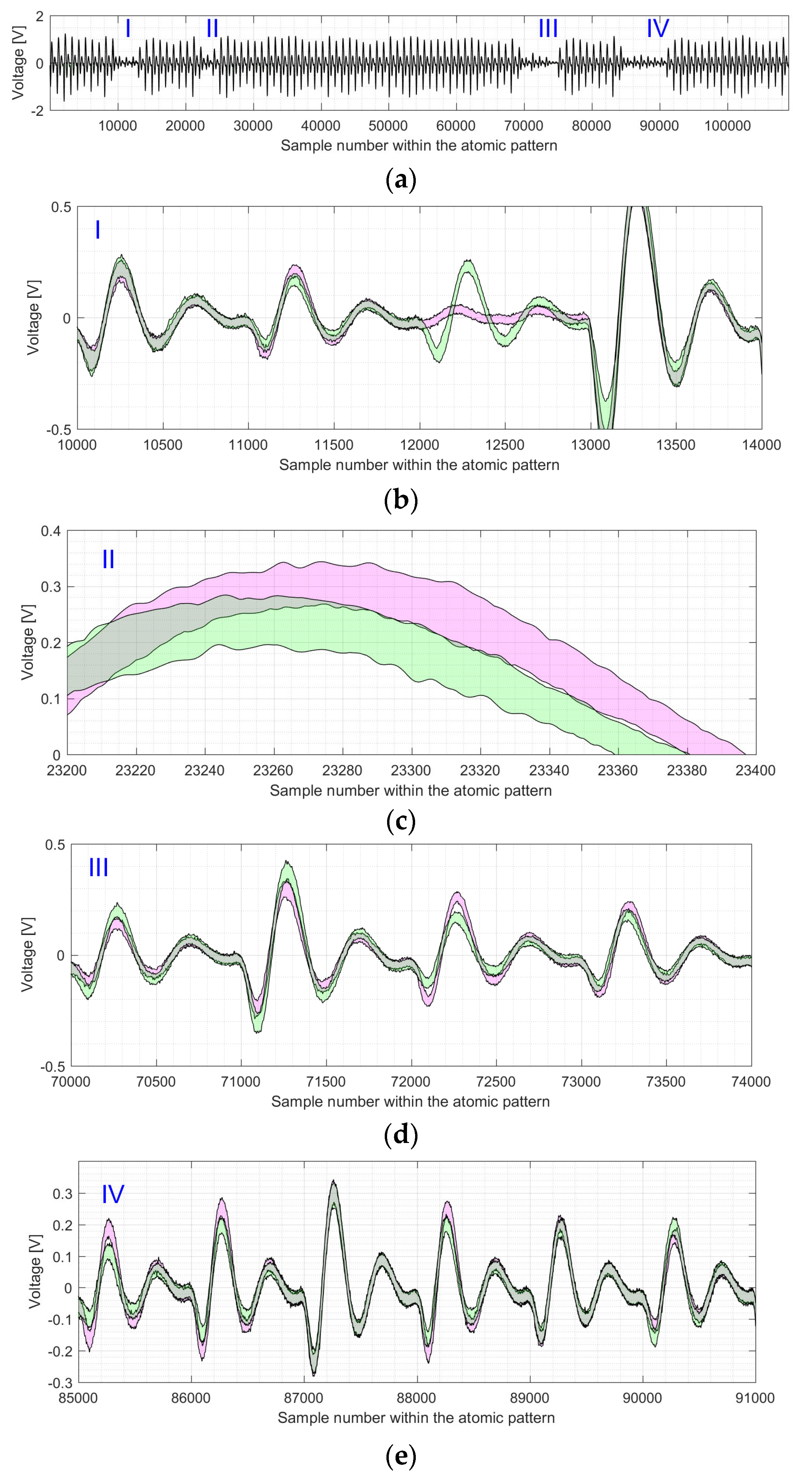
We use an example of the electromagnetic trace for EC
P-224 to visualize the difference between the shapes of the point doubling and point addition atomic patterns, indicated by I–IV (see
Figure 11a). Parts I–IV are depicted—zoomed in—in
Figure 11b–e. The shapes of point additions and point doublings are represented by magenta and green areas, respectively.
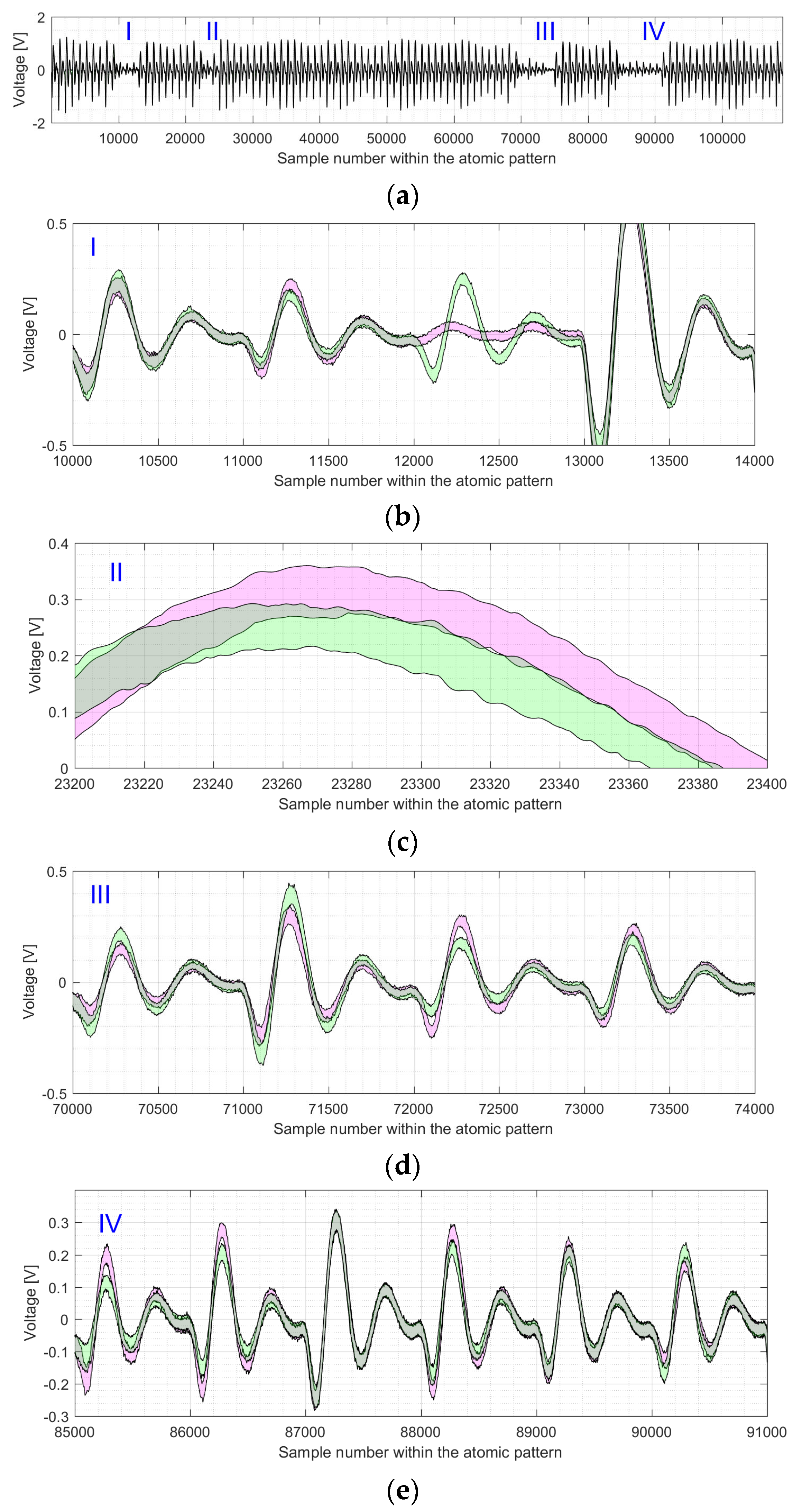
As it can be seen in
Figure 11 and
Figure 12, the four regions with an inactive multiplier differ significantly in the level of the SCA leakage. Please note that the figures have different y-axis scales. The most “visible” leakage is located in the 13th clock cycle of the atomic pattern (see
Figure 11b and
Figure 12b). The green and magenta shapes are completely separated from one another in most of the points for the x-axis values in the range between 12,000 and 13,000. The leakage in clock cycle 24 is almost “invisible” as there is only a small separation for the x-range between 23,330 and 23,380 in
Figure 11c and close to the sample number 23,320 in
Figure 12c. From the designers’ point of view, the best case in terms of resistance against simple analysis attacks corresponds to the completely gray areas (i.e., the overlapping one), where the operation execution profiles cannot be distinguished from each other.
The multiplier is a big block of our
kP design. As it can be seen from
Table 3, it consumes all the DSP blocks, almost half of the LUTs (49.94%) and 21.92% of flip-flops required by the whole design. Its energy consumption is high in comparison to other design blocks. Thus, the activity of the multiplier is a type of noise that can hide the activity of other blocks. In the next section, we demonstrate how the multiplier’s activity can reduce the success of horizontal attacks as well as simple analysis attacks as a particular case.
Figure 12 shows the difference between the shapes of atomic patterns, i.e., point doublings and point additions, for the electromagnetic trace of the EC
P-256 kP execution.
6. Influence of Dummy Partial Multiplications on the Design Resistance
In our recent works [
29,
30,
31], we investigated the influence of the activity of different field multipliers on the resistance of
kP designs against horizontal SCA attacks. In [
29], we investigated the application of the dummy activity of the multiplier as a means to reduce the vulnerability of our hardware accelerator for a single EC,
P-256, to horizontal attacks. For this investigation, the design was derived from our unified four-curve ECDSA accelerator described here. Therefore, we assume that this approach should affect the unified design in a similar way.
We modified our unified design by adding the execution of dummy partial multiplications in clock cycles where the multiplier block was not active before. The design was ported to the same FPGA, and the resource utilization is presented in
Table 6.
In comparison to the original design (see
Table 3), the modification introduced an overhead of about 1.3% in terms of LUT utilization. The most affected block is the multiplier, which was increased by 459 LUTs.
We measured four electromagnetic
kP traces on the modified design using the same inputs as in the previous experiments. We performed the
comparison to the mean attack against each of the measured traces. For the
B-233 and
B-283 elliptic curves, the attack results are practically the same with a marginal difference. The attack results for the
P-224 and
P-256 elliptic curves are presented in
Figure 13 and compared with the original design, i.e., the design without the dummy activity of the field multiplier.
As it can be seen in
Figure 13, the correctness of the key candidates for most of the clock cycles in the atomic pattern regions where the multiplier was not active, i.e., clock cycles 11 to 13, 24, 71 to 75 and 86 to 91 (see black dotted and orange lines), significantly dropped down (see violet and brown lines).
The number of key candidates for EC P-224 revealed with a correctness of more than 90% dropped down from 18 to 10 in comparison to the original design, while the best key candidate had a correctness of 97.49%. For EC P-256, the number of key candidates with a correctness of more than 90% dropped down from 20 to 9. The best key candidate had a correctness of 95.78%. Thus, the application of dummy partial multiplications reduced the success of the comparison to the mean attack.
Additionally, we repeated the simple analysis attack against the design with dummy partial multiplications using traces of the P-224 and P-256 kP executions. As a result, we discovered 17 out of 109,000 samples that allow revealing the full key for the P-224 trace only. All “leaky” samples were located in clock cycle 13 of the atomic pattern.
The number of samples that allow revealing the full key decreased from 994 down to 17 samples for EC P-224 and from 1122 to 0 samples for EC P-256.
The differences in the shapes of the point doublings and point additions are demonstrated in
Figure 14a,b for clock cycle 13 of the atomic pattern for
P-224 and
P-256, respectively.


