
A Highly Efficient RF-DC Converter for Energy Harvesting Applications Using a Threshold Voltage Cancellation Scheme

 ,
,  ,
,  , ,
, ,
Abstract
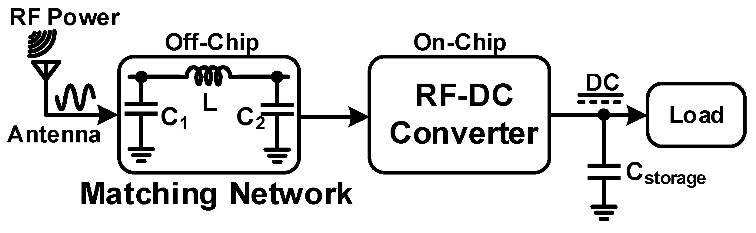
:1. Introduction
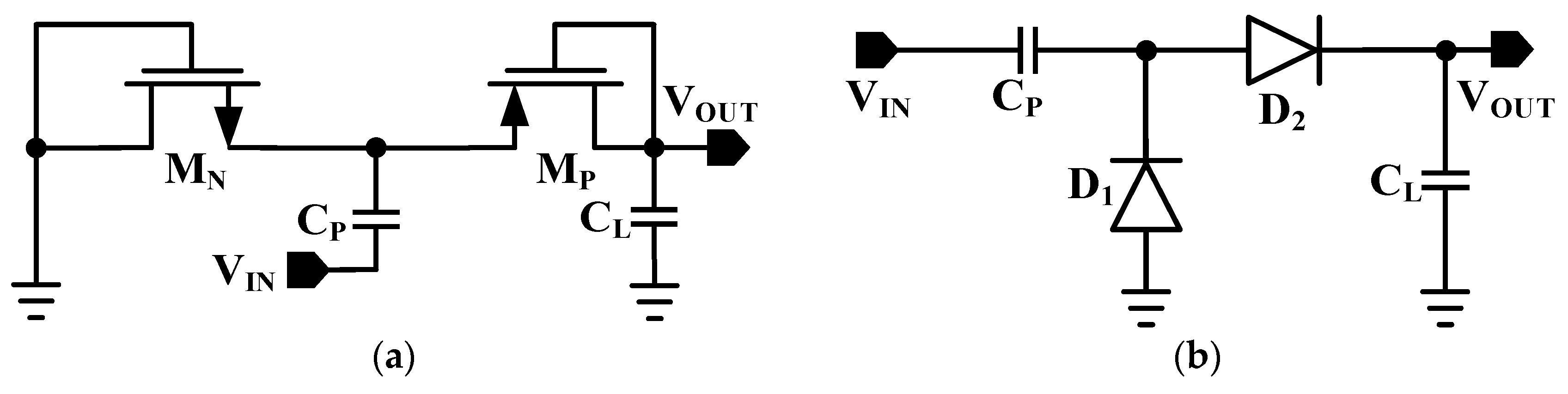
2. Self Vth Cancellation Scheme
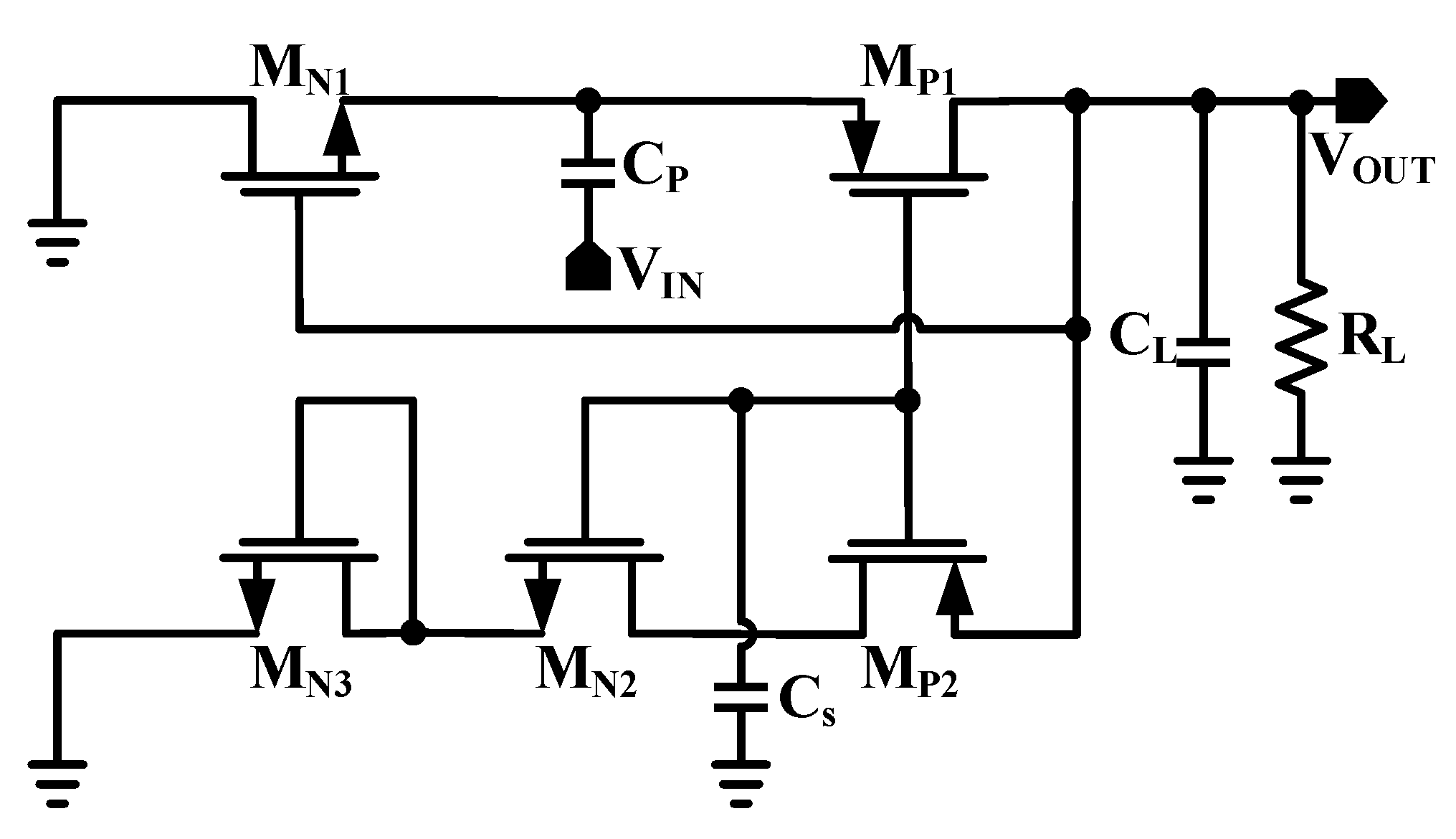
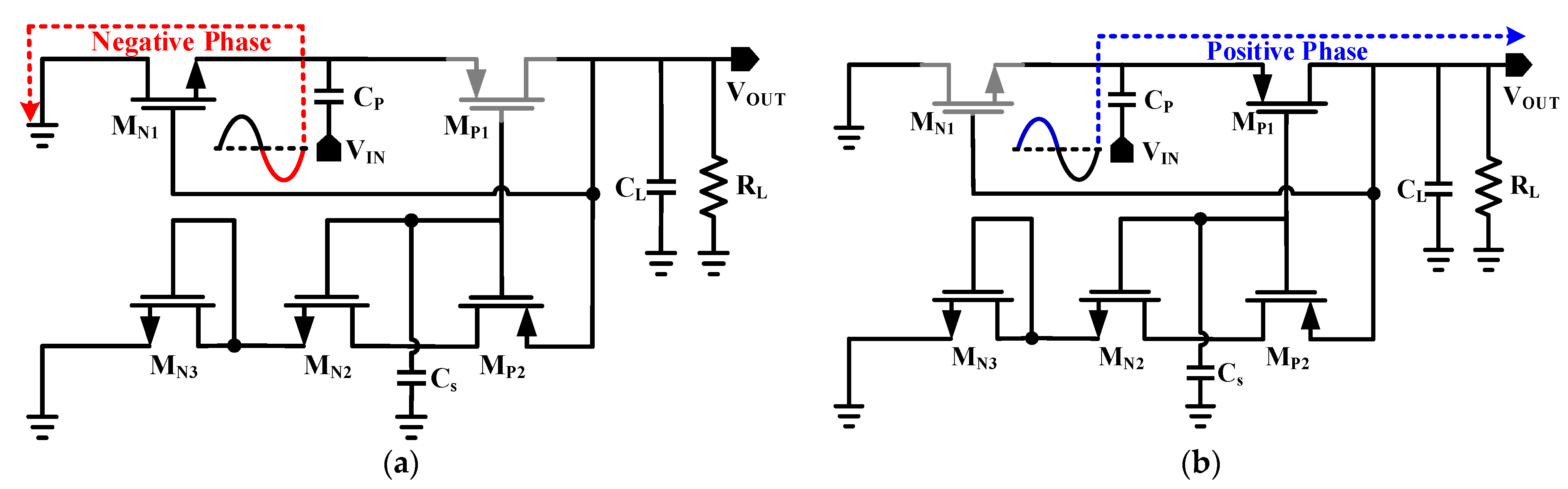
3. Proposed RF-DC Converter
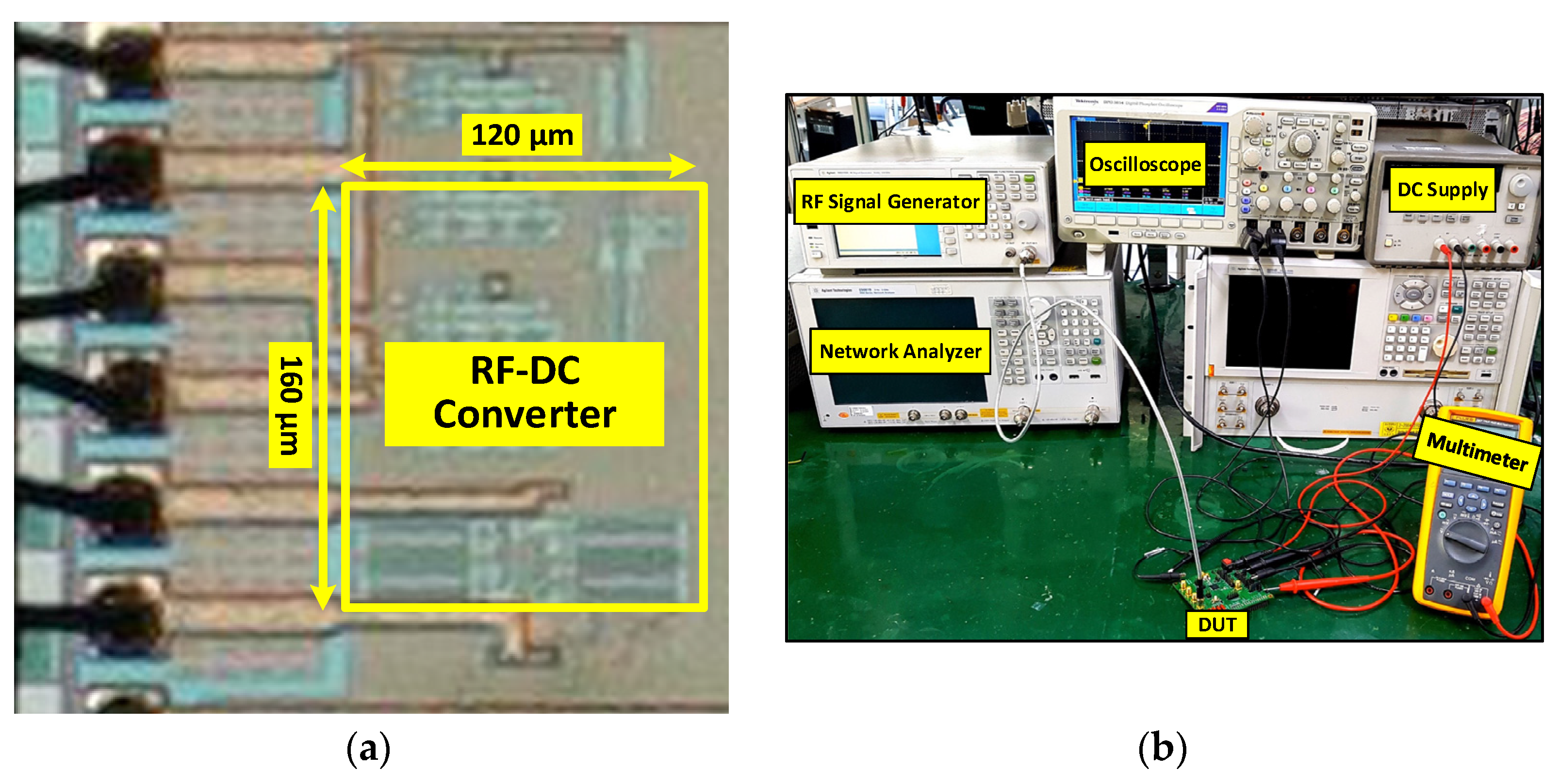
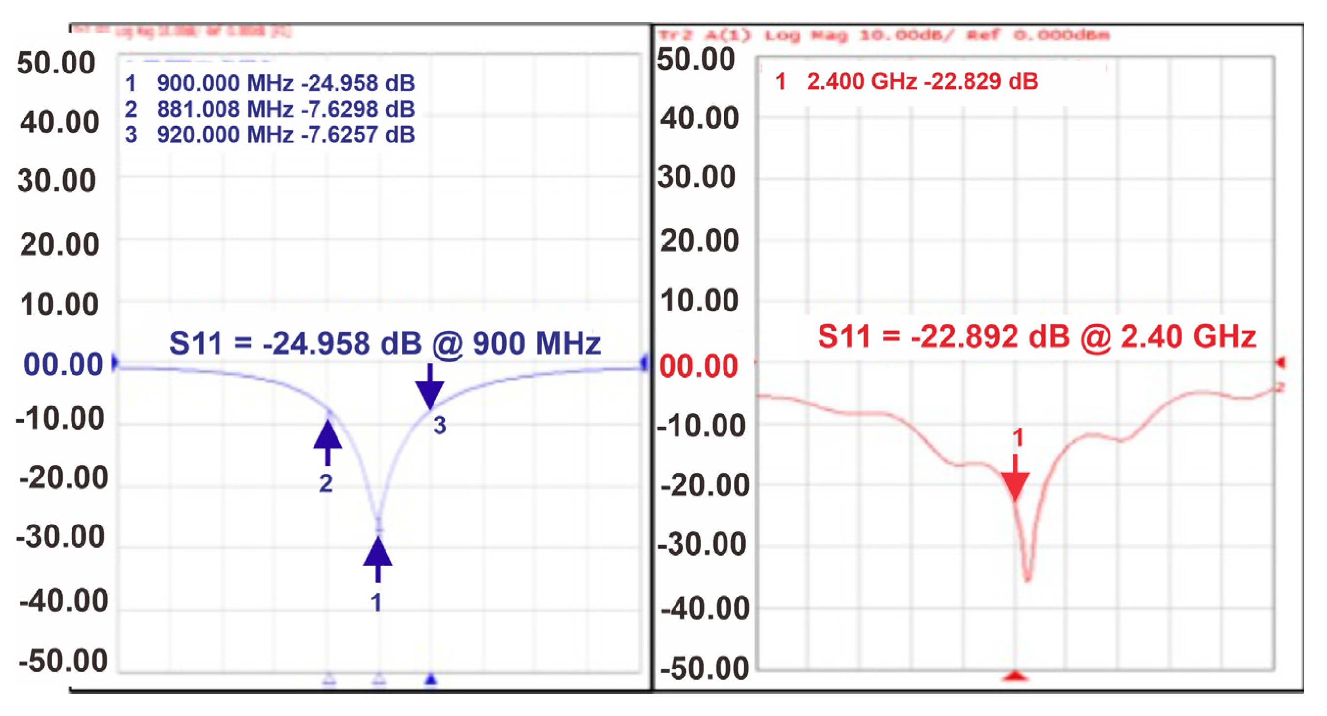
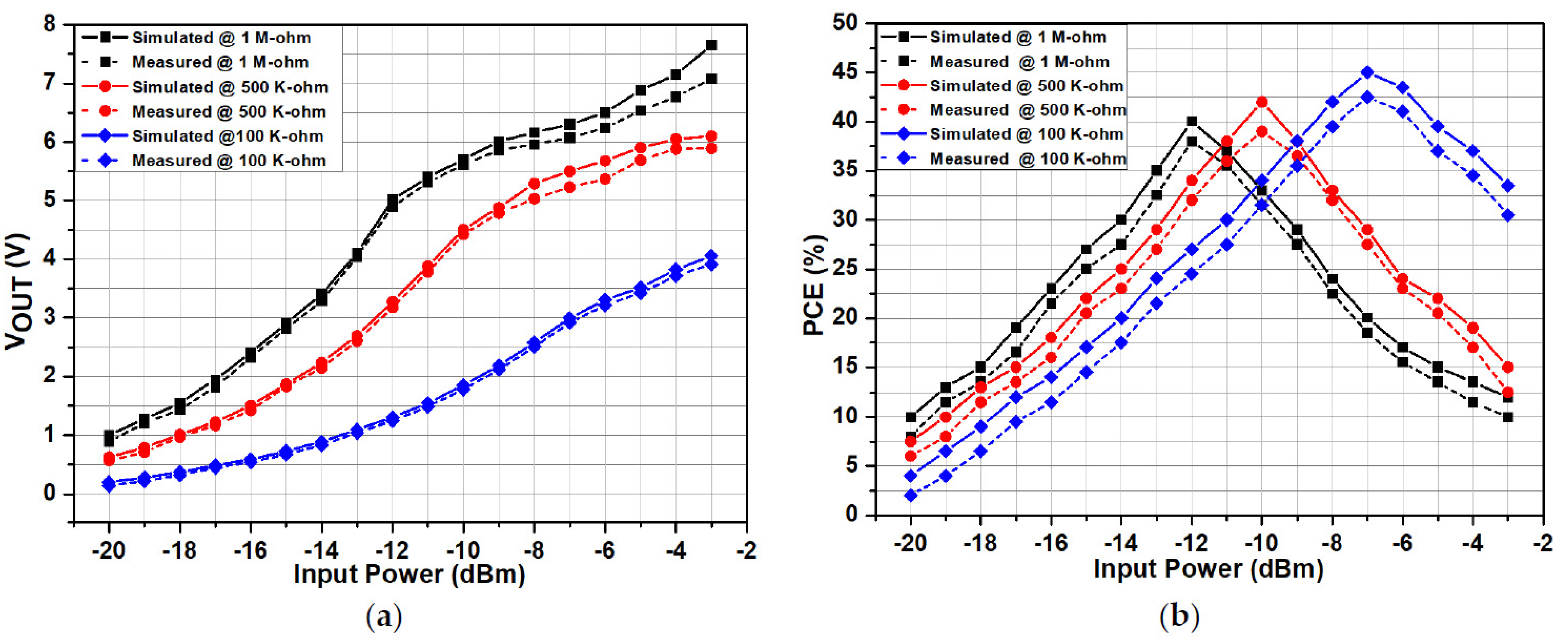
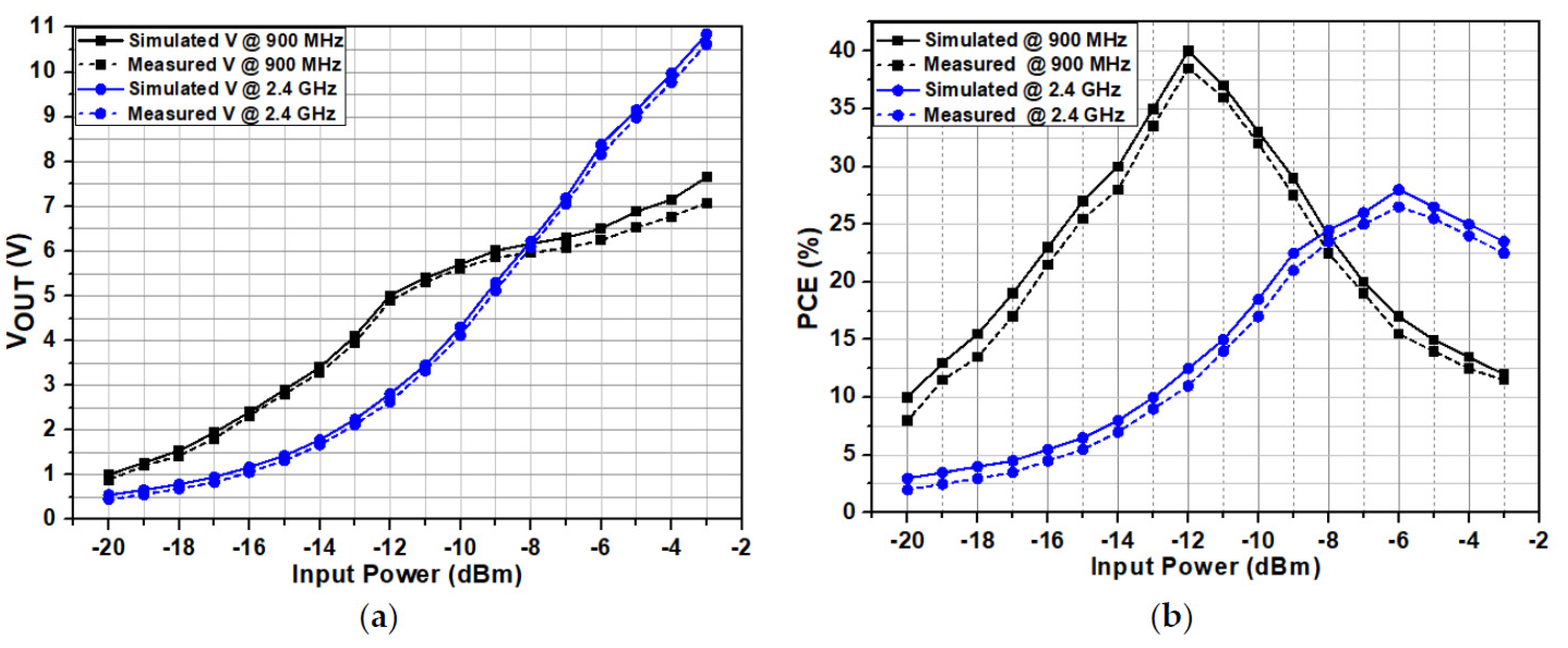
4. Measurement Results
5. Conclusions
Author Contributions
Funding
Institutional Review Board Statement
Informed Consent Statement
Data Availability Statement
Acknowledgments
Conflicts of Interest
References
- Stoopman, M.; Keyrouz, S.; Visser, J.H.; Philips, K.; Serdijn, A.W. Co-design of a CMOS rectifier and small loop antenna for highly sensitive RF energy harvesters. IEEE J. Solid-State Circuits 2014, 49, 622–634. [Google Scholar] [CrossRef]
- Hameed, Z.; Moez, K. A 3.2 V–15 dBm adaptive threshold-voltage compensated RF energy harvester in 130 nm CMOS. IEEE Trans. Circuits Syst. I Regul. Pap. 2015, 62, 948–956. [Google Scholar] [CrossRef]
- Nakamoto, H.; Yamazaki, D.; Yamamoto, T.; Kurata, H.; Yamada, S.; Mukaida, K.; Ninomiya, T.; Ohkawa, T.; Masui, S.; Gotoh, K. A Passive UHF RF Identification CMOS Tag IC Using Ferroelectric RAM in 0.35 µm CMOS Technology. IEEE J. Solid-State Circuits 2006, 42, 101–110. [Google Scholar] [CrossRef]
- Kotani, K.; Sasaki, A.; Ito, T. High-efficiency differential-drive CMOS rectifier for UHF RFIDs. IEEE J. Solid-State Circuits 2009, 44, 3011–3018. [Google Scholar] [CrossRef]
- Lazaro, O.; Rincón-Mora, G.A. A Nonresonant Self-Synchronizing Inductively Coupled 0.18m CMOS Power Receiver and Charger. IEEE J. Emerg. Sel. Top. Power Electron. 2014, 3, 261–271. [Google Scholar] [CrossRef]
- Bito, J.; Hester, J.G.; Tentzeris, M.M. Ambient RF energy harvesting from a two-way talk radio for flexible wearable wireless sensor devices utilizing inkjet printing technologies. IEEE Trans. Microw. Theory Tech. 2015, 63, 4533–4543. [Google Scholar] [CrossRef]
- Kotani, K.; Ito, T. High-efficiency CMOS rectifier circuit with self-Vth-cancellation and power regulation functions for UHF RFIDs. In Proceedings of the 2007 IEEE Asian Solid-State Circuits Conference, Jeju, Korea, 12–14 November 2007; pp. 119–122. [Google Scholar]
- O’Driscoll, S.; Poon, A.S.; Meng, T.H. An mm-sized implantable power receiver with adaptive link compensation. In Proceedings of the 2009 IEEE International Solid-State Circuits Conference-Digest of Technical Papers, San Francisco, CA, USA, 8–12 February 2009; pp. 294–295. [Google Scholar]
- Kuhn, V.; Lahuec, C.; Seguin, F.; Person, C. A multi-band stacked RF energy harvester with RF-to-DC efficiency up to 84%. IEEE Trans. Microw. Theory Tech. 2015, 63, 1768–1778. [Google Scholar] [CrossRef]
- Mikeka, C.; Arai, H. Design issues in radio frequency energy harvesting system. In Sustainable Energy Harvesting Technologies—Past, Present and Future; IntechOpen: London, UK, 2011; pp. 235–256. [Google Scholar]
- Li, C.J.; Lee, T.C. 2.4-GHz high-efficiency adaptive power. IEEE Trans. Very Large Scale Integr. (VLSI) Syst. 2013, 22, 434–438. [Google Scholar] [CrossRef]
- Dehghani, S.; Johnson, T. A 2.4-GHz CMOS class-E synchronous rectifier. IEEE Trans. Microw. Theory Tech. 2016, 64, 1655–1666. [Google Scholar] [CrossRef]
- Mansour, M.M.; Ichihashi, M.; Kanaya, H. Wide-band and efficiency-improved 0.18 um CMOS RF differential rectifier for wireless energy harvesting. In Proceedings of the 2019 IEEE Asia-Pacific Microwave Conference (APMC), Singapore, 10–13 December 2019; pp. 141–143. [Google Scholar]
- Lee, D.; Kim, T.; Kim, S.; Byun, K.; Kwon, K. A CMOS rectifier with 72.3% RF-to-DC conversion efficiency employing a tunable impedance matching network for ambient RF energy harvesting. In Proceedings of the 2018 International SoC Design Conference (ISOCC), Daegu, Korea, 12–15 November 2018; pp. 259–260. [Google Scholar]
- Li, X.; Lu, Y.; Huang, M.; Martins, R.P. A 2.4-GHz mid-field CMOS wireless power receiver achieving 46% maximum PCE and 163-mW output power. IEEE Trans. Circuits Syst. II Express Briefs 2019, 67, 360–364. [Google Scholar] [CrossRef]
- Kim, S.Y.; Abbasizadeh, H.; Rikan, B.S.; Oh, S.J.; Jang, B.G.; Park, Y.J.; Khan, D.; Nga, T.T.K.; Kang, K.T.; Pu, Y.G.; et al. A-20 to 30 dBm input power range wireless power system with an MPPT-based reconfigurable 48% efficient RF energy harvester and 82% efficient A4WP wireless power receiver with open-loop delay compensation. IEEE Trans. Power Electron. 2018, 34, 6803–6817. [Google Scholar] [CrossRef]
- Khan, D.; Abbasizadeh, H.; Kim, S.Y.; Khan, Z.H.N.; Shah, S.A.A.; Pu, Y.G.; Hwang, K.C.; Yang, Y.; Lee, M.; Lee, K.Y. A design of ambient RF energy harvester with a sensitivity of− 21 dBm and power efficiency of 39.3% using internal threshold voltage compensation. Energies 2018, 11, 1258. [Google Scholar] [CrossRef] [Green Version]
- Yan, L.; Haojuan, D.; Mo, H.; Man, K.L.; Sai, W.S.; Seng, P.U.; Rui, P.M. A Wide Input Range Dual-Path CMOS Rectifier for RF Energy Harvesting. IEEE Trans. Circuits Syst. 2017, 64, 166–170. [Google Scholar]
- Papotto, G.; Carrara, F.; Palmisano, G. A 90-nm CMOS threshold-compensated RF energy harvester. IEEE J. Solid-State Circuits 2011, 46, 1985–1997. [Google Scholar] [CrossRef]
- Khan, D.; Oh, S.J.; Shehzad, K.; Verma, D.; Khan, Z.H.N.; Pu, Y.G.; Lee, M.; Hwang, K.C.; Yang, Y.; Lee, K.Y. A CMOS RF energy harvester with 47% peak efficiency using internal threshold voltage compensation. IEEE Microw. Wirel. Compon. Lett. 2019, 29, 415–417. [Google Scholar] [CrossRef]
- Scorcioni, S.; Larcher, L.; Bertacchini, A. A reconfigurable differential CMOS RF energy scavenger with 60% peak efficiency and-21 dBm sensitivity. IEEE Microw. Wirel. Compon. Lett. 2013, 23, 155–157. [Google Scholar] [CrossRef]
- Abouzied, M.A.; Ravichandran, K.; Sánchez-Sinencio, E. A fully integrated reconfigurable self-startup RF energy-harvesting system with storage capability. IEEE J. Solid-State Circuits 2017, 52, 704–719. [Google Scholar] [CrossRef]
- Khan, D.; Oh, S.J.; Shehzad, K.; Basim, M.; Verma, D.; Pu, Y.G.; Lee, M.; Hwang, K.C.; Yang, Y.; Lee, K.Y. An efficient reconfigurable RF-DC converter with a wide input power range for RF energy harvesting. IEEE Access 2020, 8, 79310–79318. [Google Scholar] [CrossRef]
- Hameed, Z.; Moez, K. Hybrid forward and a backward threshold-compensated RF-DC power converter for RF energy harvesting. IEEE J. Emerg. Sel. Top. Circuits Syst. 2014, 4, 335–343. [Google Scholar] [CrossRef]
- Munir, A.A.-A.; Sami, R.A.-B. Hybrid Internal Vth Cancellation Rectifiers for RF Energy Harvesting. IEEE Access 2020, 8, 51976–51980. [Google Scholar]
- Noghabaei, S.M.; Radin, R.L.; Savaria, Y.; Sawan, M. A High-Sensitivity Wide Input-Power-Range Ultra-Low-Power RF Energy Harvester for IoT Applications. IEEE Trans. Circuits Syst. I Regul. Pap. 2022, 69, 440–451. [Google Scholar] [CrossRef]
- Hsieh, P.; Chiang, T. An RF energy harvester with 35.7% PCE at PIN of −15 dBm. In Proceedings of the Symposium on VLSI Circuits, Kyoto, Japan, 11–13 June 2013; pp. C224–C225. [Google Scholar]
- Khan, D.; Oh, S.J.; Yeo, S.K.; Ryu, Y.; In, S.H.; Rad, R.E.; Ali, I.; Pu, Y.G.; Yoo, S.S.; Lee, M.; et al. A High-Efficient Wireless Power Receiver for Hybrid Energy-Harvesting Sources. IEEE Trans. Power Electron. 2021, 36, 11148–11162. [Google Scholar] [CrossRef]
- Hameed, Z.; Moez, K. Fully-integrated passive threshold-compensated PMOS rectifier for RF energy harvesting. In Proceedings of the IEEE 56th International Midwest Symposium on Circuits and Systems (MWSCAS), Columbus, OH, USA, 4–7 August 2013; pp. 129–132. [Google Scholar]


| Parameters | This Work | [2] | [13] | [18] | [22] | [23] | [24] |
|---|---|---|---|---|---|---|---|
| 2015 | 2019 | 2017 | 2017 | 2020 | 2014 | ||
| Technology (nm) | 180 | 130 | Diode-Based | 65 | 180 | 180 | 130 |
| Energy harvesting | RF | RF | RF | RF | RF | RF | RF |
| Frequency (GHz) | 0.9/2.4 | 0.902~0.928 | 2.45 | 0.953 | 0.915 | 0.902 | 0.915 |
| Load (MΩ) | 1 | 1 | 0.2 | 0.147 | 1 | 0.2 | 1 |
| Input power (dBm) | −12/−6 | −15 | 13 | −10 | −2 | −8 | −16.8 |
| DC output (V) | 4.8/8.1 | 3.2 | 1.7 | 2.6 | 2.4 | 3.23 | 2.2 |
| PCE (%) | 38.5/26.5 | 32 | 37.5 | 36.5 | 27 | 33 | 22.6 |
| Effective Area | 0.19 mm2 | - | 0.74 mm2 | 0.47 mm2 | - | 0.105 mm2 | - |
| Sensitivity: 1 V for 1 MΩ | −20 dBm | −20.5 dBm | - | −17.5 dBm | 14.8 dBm | −20.2 dBm | −21.6 dBm |
Publisher’s Note: MDPI stays neutral with regard to jurisdictional claims in published maps and institutional affiliations. |
© 2022 by the authors. Licensee MDPI, Basel, Switzerland. This article is an open access article distributed under the terms and conditions of the Creative Commons Attribution (CC BY) license (https://creativecommons.org/licenses/by/4.0/).
Share and Cite
Basim, M.; Khan, D.; Ain, Q.U.; Shehzad, K.; Shah, S.A.A.; Jang, B.-G.; Pu, Y.-G.; Yoo, J.-M.; Kim, J.-T.; Lee, K.-Y. A Highly Efficient RF-DC Converter for Energy Harvesting Applications Using a Threshold Voltage Cancellation Scheme. Sensors 2022, 22, 2659. https://doi.org/10.3390/s22072659
Basim M, Khan D, Ain QU, Shehzad K, Shah SAA, Jang B-G, Pu Y-G, Yoo J-M, Kim J-T, Lee K-Y. A Highly Efficient RF-DC Converter for Energy Harvesting Applications Using a Threshold Voltage Cancellation Scheme. Sensors. 2022; 22(7):2659. https://doi.org/10.3390/s22072659
Chicago/Turabian StyleBasim, Muhammad, Danial Khan, Qurat Ul Ain, Khuram Shehzad, Syed Adil Ali Shah, Byeong-Gi Jang, Young-Gun Pu, Joon-Mo Yoo, Joon-Tae Kim, and Kang-Yoon Lee. 2022. "A Highly Efficient RF-DC Converter for Energy Harvesting Applications Using a Threshold Voltage Cancellation Scheme" Sensors 22, no. 7: 2659. https://doi.org/10.3390/s22072659