Article

Modular Single-Stage Three-Phase Flyback Differential Inverter for Medium/High-Power Grid Integrated Applications

by
Ahmed Ismail M. Ali
1,2,*,
Cao Anh Tuan
1,
Takaharu Takeshita
1,
Mahmoud A. Sayed
2 and
Zuhair Muhammed Alaas
3
1
Electrical and Mechanical Engineering Department, Nagoya Institute of Technology, Nagoya 466-8555, Japan
2
Electrical Engineering Department, South Valley University, Qena 83523, Egypt
3
Electrical Engineering Department, Jazan University, Jazan 45142, Saudi Arabia
*
Author to whom correspondence should be addressed.
Sensors 2022, 22(5), 2064; https://doi.org/10.3390/s22052064
Submission received: 8 February 2022 / Revised: 1 March 2022 / Accepted: 1 March 2022 / Published: 7 March 2022

Abstract

:
This paper proposes a single-stage three-phase modular flyback differential inverter (MFBDI) for medium/high power solar PV grid-integrated applications. The proposed inverter structure consists of parallel modules of flyback DC-DC converters based on the required power level. The MFBDI offers many features for renewable energy applications, such as reduced components, single-stage power processing, high-power density, voltage-boosting property, improved footprint, flexibility with modular extension capability, and galvanic isolation. The proposed inverter has been modelled, designed, and scaled up to the required application rating. A new mathematical model of the proposed MFBDI is presented and analyzed with a time-varying duty-cycle, wide-range of frequency variation, and power balancing in order to display its grid current harmonic orders for grid-tied applications. In addition, an LPF-based harmonic compensation strategy is used for second-order harmonic component (SOHC) compensation. With the help of the compensation technique, the grid current THD is reduced from 36% to 4.6% by diminishing the SOHC from 51% to 0.8%. Moreover, the SOHC compensation technique eliminates third-order harmonic components from the DC input current. In addition, a 15% parameters mismatch has been applied between the flyback parallel modules to confirm the modular operation of the proposed MFBDI under modules divergence. In addition, SiC MOSFETs are used for inverter switches implementation, which decrease the inverter switching losses at high-switching frequency. The proposed MFBDI is verified by using three flyback parallel modules/phase using PSIM/Simulink software, with a rating of 5 kW, 200 V, and 50 kHz switching frequency, as well as experimental environments.

1. Introduction

Recently, the COVID-19 pandemic has disturbed most energy resources and prevented the importation and exportation of fuel between the countries. In addition, the large need for energy in human life has increased the requirements for renewable energy sources (RESs) [1]. Among the different RESs, photovoltaic (PV) is the most common and promising energy resource due to its operation sustainability in the distributed generation systems, which provide freely available energy hunks for humankind [2,3,4]. Therefore, different single-stage and multistage inverter topologies have been developed as an attractive key for grid-integrated RESs at different climatic conditions [5,6,7,8]. In comparison with the multistage inverter, single-stage structures offer reliable, compact, high power density, and improved footprint converters [9,10,11,12,13]. Different multilevel inverter (MLI) structures are presented for high power-quality stand-alone and grid-integrated PV applications [6,8]. However, large-size line-frequency transformers are required in many topologies that decrease the system power density and increase the required components. Owing to galvanic isolation necessity, high-frequency transformer (HFT)-based inverters have been developed for inverter footprint and efficiency improvement [14,15]. HFT-based inverters start with a two-stage operation using a decoupling capacitor/inductor, which increases the required components number, size, and system overall footprint [16,17,18,19].
Motivated by the preceding drawbacks of the two-stage inverter, single-stage inverter architectures have been presented in single/three-phase applications with continuous DC-input current waveform [6]. In [6], single-phase single-stage isolated DC-AC MLI is presented for stand-alone and grid-integrated PV applications. Despite the improved power quality of these converters, many power switches are required. Therefore, PV-microinverters have been widely recommended in recent decades due to their features such as low cost, compactness, reliability, improved footprint, and galvanic isolation requirements for grid-connected applications [20,21]. Microinverter-based flyback DC-DC modules are commonly utilized in combined with the unfolding circuit due to the reduced passive components, a low number of switches, and a simple control strategy [22,23]. However, the recently available PV-microinverters are applicable for low-power purposes (below 200 W). Therefore, DC-DC converter-based differential inverter topologies have been presented for isolated single-stage high power applications. In [24,25], single-phase differential inverters have been introduced with buck and boost converter modules for compact and efficient operation. However, the presented topologies suffer from the high voltage stress over the converter components [26]. In [27], the Cuk differential inverter has been presented for single-phase applications; however, it requires a comparatively increased number of components. Therefore, a single-phase single-stage Cuk differential inverter is proposed for PV direct power conversion with compact and high-efficiency operation [28,29]. However, the proposed control strategy increases the ripples of the DC input current that decreases the input power factor. For three-phase purposes, a three-phase single-stage Cuk differential inverter is proposed for PV applications [30,31]. However, three separate input filters are required for continuous input current operation for RESs. In [32], the three-phase single-stage SEPIC differential inverter is presented with only four switches. However, the presented topology is applicable for low-power applications due to the drop of grid isolation.
In comparison with the former buck-boost based differential inverter topologies, the proposed modular flyback inverter structure has the following merits; it utilizes a reduced number of passive elements and power switches, single-stage DC-AC conversion, voltage boosting, modularity, compact size, and galvanic isolation property. The three-phase flyback differential inverter (FBDI) parameters design and selection, hardware implementation, and control technique were analyzed. Modular FBDI (MFBDI) was presented and analyzed for megawatt-class DC-DC converter-based inverters. Mathematical modelling of the proposed MFBDI was analyzed, which confirmed the existence of a second-order harmonic component (SOHC). In addition, SOHC compensation was achieved by considering an LPF-based harmonic elimination strategy for grid current THD reduction in order to follow the IEC61000-3-2 (Class-A) harmonic standard limit. In order to confirm the modular operation of the proposed MFBDI, a 15% mismatch between the paralleled flyback DC-DC modules was used with three-paralleled modules in each phase for an overall rating of 5 kW. It is worth mentioning that the proposed MFBDI was compared with its recent counterpart topologies, by considering the number of components and passive elements, modulation scheme, number of control loops, controller, switching frequency, current THD, number of required sensors, power rating, and the utilized switches ratings as depicted in Table 1. Obviously, the proposed converter utilizes a reduced number of components, control loops, and sensors that enhances the system footprint and cost.
The paper manuscript has been organized as follows: Section 2 illustrates the modular operation of the proposed MFBDI and its mathematical model. In addition, the flyback converter parameters’ design and selection, as well as hardware implementation, are analyzed in Section 3. Moreover, the MFBDI control scheme and the system simulation and experimental verifications are illustrated and analyzed in Section 4 and Section 5, respectively. Finally, Section 6 concludes the paper’s contributions and verifications.

2. Modular Flyback Differential Inverter

The proposed MFBDI consists of N number of isolated DC-DC flyback modules, which are connected in parallel at the input and output sides, Input Parallel Output Parallel (IPOP), as depicted in Figure 1. However, the three-phase configuration is connected in parallel at the DC input side and differentially on the grid side. In addition, the power rating of the MFBDI is simply N-multiple of single module power rating, where N is a number of parallel modules in each phase as shown in Figure 1 and Figure 2. Hence, the operation principles of a single flyback module and mathematical modeling of the proposed MFBDI are analyzed in this section.

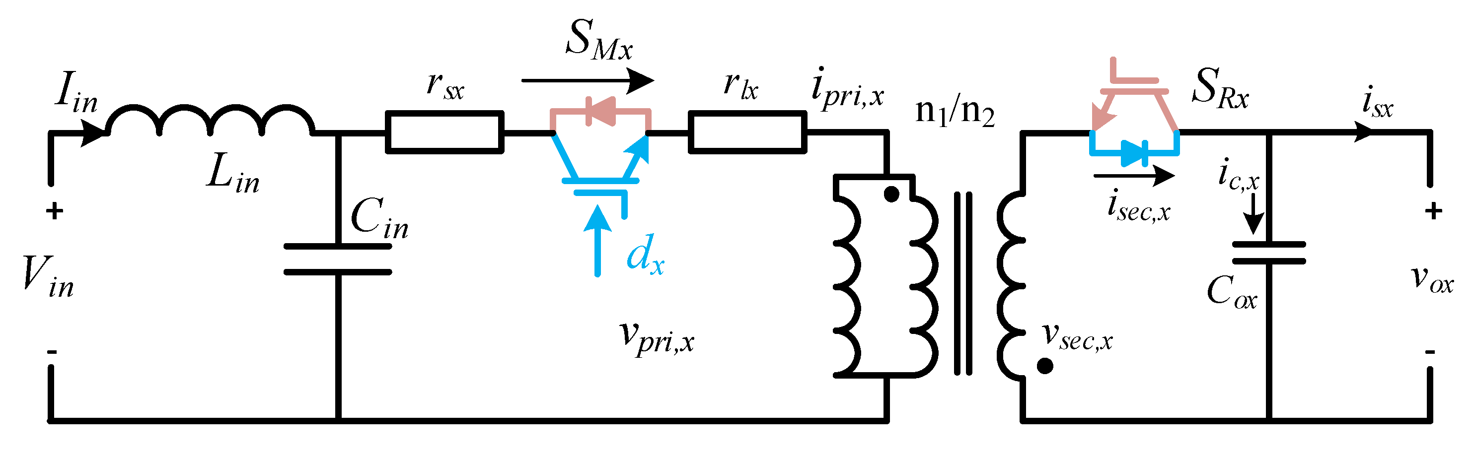
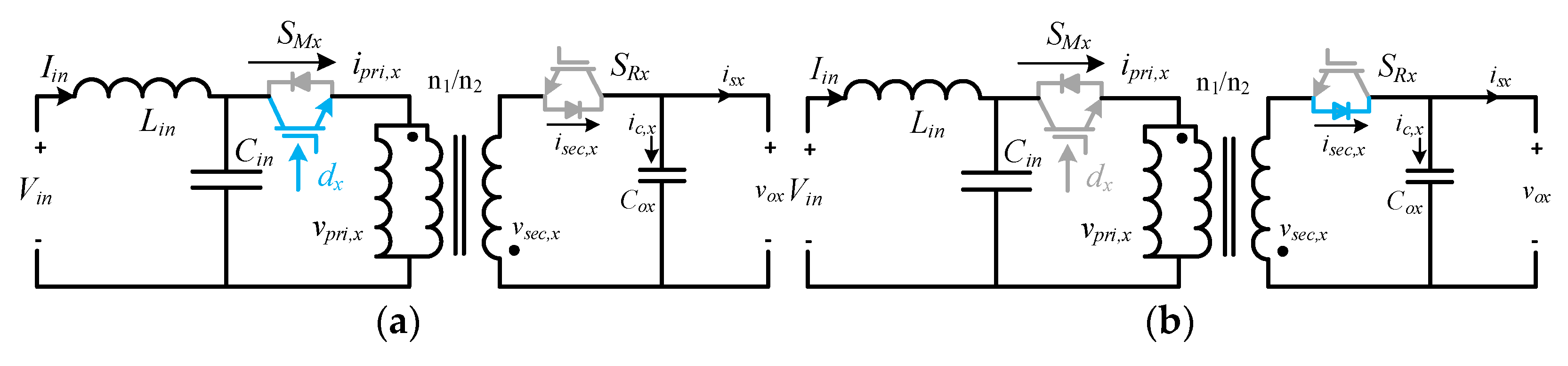
2.1. Single Flyback Module Operation

Figure 1 shows the power stage of the proposed MFBDI, where the power stage of one phase of the proposed MFBDI is portrayed in Figure 2. A one-phase of the proposed MFBDI is consists of three parallel modules to increase the system power rating to triple-level (N = 3). A single module is composed of; a single LC input low-pass filter (Lin, Cin), two SiC-MOSFET switches (SMx, and SRx), a flyback high-frequency transformer (FB-HFT), a robust designed snubber-circuit, and a single output capacitor (COx). The proposed inverter is controlled with a time-varying duty-cycle (dx). Thus, the generated output voltage at the inverter terminal is DC-voltage with a sinusoidal envelope as depicted in Figure 3. Obviously, the MFBDI terminal voltage contains a DC voltage offset due to the unipolar operation of the flyback modules, which is canceled at the grid side by a differential connection. Hence, a sinusoidal output voltage can be synthesized for sinusoidal grid injected current. In addition, the phase-shift between the flyback modules of the same phase is 0° and 120° between the DC-DC modules of different phases. In addition, a single-module operation can be divided into two operational modes [36]: a. Turing-ON of primary switch passes the current in the primary side of FB-HFT, which stores energy in the HFT magnetic inductance as a magnetic field. The grid-current is maintained by the inverter terminal capacitor during this mode. b. As the main switch turns-OFF, the stored energy releases through the body-diode of the synchronous switch to supply the grid-current and charge the output capacitor as a Current Source Inverter (CSI). The operational modes of a one-phase/single module of the proposed three-phase MFBDI with its bidirectional power flow are portrayed in Figure 4. Moreover, the flyback converter operates temporarily to transfer the power from input to output sides, as clearly portrayed in Figure 5a,b.
The input DC-voltage/PV voltage is assumed to be constant due to LC filter’s large capacitance at the input side. The proposed MFBDI is controlled via continuous conduction-mode (CCM), in which the transformer core incompletely demagnetizes in one switching cycle. The demagnetizing effect of the MFBDI transformer has a negligible effect on the inverter output power-factor as the magnetizing energy is very low compared with the transferred energy to the output side [36]. In addition, the voltage spikes are limited by a stringently designed snubber-circuit.

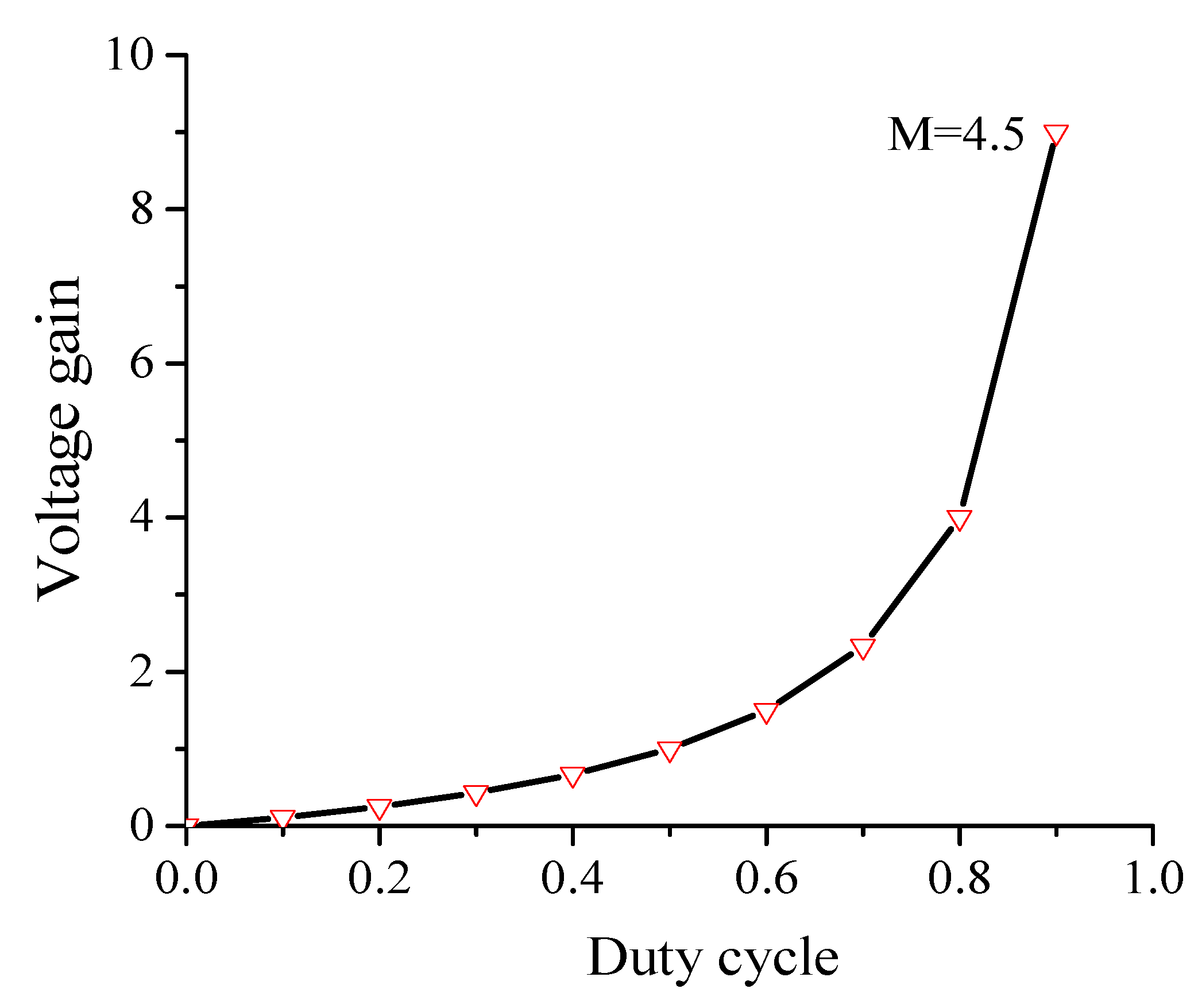
2.2. Mathematical Model of MFBDI

Generally; as the proposed MFBDI is supplied with DC-voltage at the input-side and controlled by time-varying duty-cycle, an output-voltage with sinusoidal envelope can be synthesized at the terminal of each module considering the converter conversion ratio as follows:
M ( d ) = n d x d x · ( 1 d x · V d n · d x · V i n ) × ( 1 1 + r l x d x n 2 R e q · d x 2 + r s x d x n 2 R e q · d x 2 + r d R e q · d x )
where,
M(d) is the input-to-output voltage conversion ratio,
Vin is the input DC voltage,
n is the transformer turns ratio, n = n2/n1,
dx is the main switch duty cycle,
Vd is the voltage drop over the diode,
rlx is the primary inductor resistance,
Req is the grid equivalent resistance,
rsx is the MOSFET semiconductor switch on-resistance,
rd is the diode on-resistance.
Based on Equation (1), the resistances of the inductor, switches, and diodes limit the MFBDI voltage gain. Thus, maintaining these resistances at a low level is an important aspect [37]. An important issue of the buck-boost-based inverter is the nonlinear relation between the converter input and output, which results in the low-order harmonics in the grid injected currents. In addition, it results in high voltage stress over power components that increases the inverter power loss and diminishes its efficiency. The voltage/current stress over the proposed MFBDI, related to its parameters, is listed in Table 2. Thus, the selection of the different elements rating can be decided to avoid components failure and unstable running operation due to the presence of the passive elements. The passive-elements values determine the system stability over the wide range of duty-cycle and frequency variations.
The switching waveforms of a single flyback module is depicted in Figure 6, which portrays the three-phase duty-cycles (dx), HFT primary switched voltage and current waveforms (vpri_x, ipri_x), switched voltage and current waveforms of HFT secondary side (vsec_x, isec_x), capacitor current icx, three-phase output voltages (vox), three-phase grid-voltages (vx), and three-phase grid-injected currents (isx). For ideal operation of the proposed three-phase inverter, the three-phase balanced voltages and grid currents can be formulated as follows:
[ v s u ( t ) v s v ( t ) v s w ( t ) ] = 2 · E · [ s i n ( ω t + α ) s i n ( ω t + α 2 π 3 ) s i n ( ω t + α + 2 π 3 ) ]
[ i s u ( t ) i s v ( t ) i s w ( t ) ] = 2 · I · [ s i n ( ω t + α ) s i n ( ω t + α 2 π 3 ) s i n ( ω t + α + 2 π 3 ) ]
where E and I are the RMS values of the grid voltage and current, respectively. In addition, ω is the grid angular-frequency, and α is the arbitrary angle.
Due to the parallel connection of flyback modules sharing identical amount of power, then the total grid current can be formulated as follows:
[ i s u ( t ) i s v ( t ) i s w ( t ) ] = 2 · I · N · [ s i n ( ω t + α ) s i n ( ω t + α 2 π 3 ) s i n ( ω t + α + 2 π 3 ) ]
where N is the number of parallel modules in each phase of MFBDI.
Based on Equation (1) for the output-to-input voltage transfer ratio of the buck-boost based inverters, the ideal voltage transfer ratio can be formulated as follows:
v o x v i n = i i n , N x i s x N = d x 1 d x
where iin,Nx, isxN are the input and grid currents of module N in phase x.
Therefore, the duty cycle can be expressed as follows:
d x = v o x v o x + v i n
Evidently, the buck-boost converter input-to-output nonlinear relation results in low-frequency odd harmonics; however, the low-order even harmonics result from the modules mismatch. Therefore, the proposed MFBDI is controlled in continuous conduction-mode (CCM), in CMS merged with static linearization-strategy (SLS) for low-order odd harmonics minimization. In addition, SOHC is created by the flyback modules mismatch: hence, a secondary loop is required for SOHC elimination. With the help of the properly controlled duty cycle and the DC-DC flyback converter-based operation, the inverter synthesized output voltage has two components; DC offset voltage and line-frequency AC voltage for grid integration. The DC offset voltage is approximately equal for all modules. Thus, the output voltage can be formulated as follows:
[ v o u ( t ) v o v ( t ) v o w ( t ) ] = V d c 0 + v s x ( t ) = V d c 0 + 2 · E · [ s i n ( ω t + α ) s i n ( ω t + α 2 π 3 ) s i n ( ω t + α + 2 π 3 ) ]
To decrease the voltage stress over the switches, the peak value of AC component is adjusted to be equal to DC component (Vdc0). Thus, the inverter terminal voltages can be formulated as follows:
v o x ( t ) = V d c 0 + V d c 0 · K x = M v i n + M v i n · K x = M v i n · ( 1 + K x )
where M is the flyback converter voltage-gain and K is the instantaneous unity of three-phase waveforms:
K x = [ s i n ( ω t + α ) s i n ( ω t + α 2 π 3 ) s i n ( ω t + α + 2 π 3 ) ]
From (6) and (8), the static-linearized duty-cycle can be synthesized as follows:
d x = M ( 1 + K x ) M ( 1 + K x ) + 1
The maximum voltage-gain of the flyback module, at K = 1, can be formulated as:
M = V o x 2 v i n
where Vox is the peak value of converter terminal voltage.
Therefore, each flyback module operates with variable duty-cycle to transfer its rated power based on the required voltage transfer ration, which inspire its modular operation by increasing the number of parallel operating modules in each phase of the proposed MFBDI. Hence, the total input current to one phase (u) is the sum of all currents to each individual module:
i i n , u = m = 1 N i i n , m
Thus, the total input DC current of the MFBDI can be expressed as follows:
i d c = i i n , u + i i n , v + i i n , w
Based on (5) and (10), the output current of one-phase (u) can be formulated as follows:
i i n , N x = 0.5 M i s x N + M K · i s x N 0.5 M K 1 · i s x N
where K1 is the second-order sinusoidal constant of the inverter input current, which illustrates the circulating power between the different flyback modules at double of the line-frequency as shown in Figure 3. It can be formulated as follows:
K 1 = [ C o s ( 2 ω t + α ) C o s ( 2 ω t + α 2 π 3 ) C o s ( 2 ω t + α + 2 π 3 ) ]
Therefore, the input power to a single flyback module can be expressed as follows:
p i n , N x = 0.5 M v i n i s x N + M K · v i n i s x N 0.5 M K 1 · v i n i s x N

3. Converter Parameters Design and Selection

In the parameter selection of the proposed converter, each DC-DC flyback module is designed with reduced switching components. In addition, the designed parameters for the flyback module are listed in Table 3. The plot of flyback converter voltage gain with different duty cycles (dx = 0~0.9), based on (5) and (11), is seen in Figure 7. The main and synchronous switches of each flyback module (SMa, SRa) are complementary controlled. In addition, continuous DC input current is an important aspect for renewable energy applications, such as photovoltaics and fuel cells. Therefore, the high-frequency switched differential structure of the proposed converter, together with a single LC input filter, provides the following features: (a) it provides DC input current considering single input filter, (b) it eradicates the large electrolytic capacitor over the input PV modules, (c) it provides galvanic isolation that minimizes the EMI and CMV, and (d) it minimizes the inverter size due to the single-stage operation [30,37]. The large-signal model is used to illustrate the low-frequency component of the current and voltage waveforms to illustrate the components voltage and current stresses. Figure 8 shows the duty cycle, primary current, main switch voltage, synchronous switch current, capacitor average current, and grid-injected current. The flyback module parameters design and selection are cleared in the following sections.
Based on the system parameters that are listed in Table 3, each three-phase module of the MFBDI processes 1.6 kW. Therefore, each flyback module processes one-third of the converter power as follows:
P M o d u l e = P F B D I 3 = 1600 3 = 533.3   W
Thus, each module processes 533.3 W from the DC side to the grid side.
In addition, based on (11) the maximum voltage gain of each flyback converter can be calculated as follows:
M = v o x 2 v i n = 2 × 163.3 2 × 100 = 1.633
Therefore, the minimum and optimal value for M is (1.633) for inverter differential operation.
Moreover, the required grid-injected current can be calculated as follows:
P M o d u l e = E · i x = 533.3   W i x = 4.6185   A
where ix refers to the RMS value of the grid injected current.
Considering the maximum operating duty cycle (dx = 0.8) during the converter parameters design, the peak value of input current to the converter can be calculated as follows:
I i n = [ d x 1 d x + 1 ] · I x = 32.66   A
Consequently, the grid equivalent resistance is 25 Ω and the voltage and current stresses can be calculated as follows:
V S M x = v i n + v o x = 100 + 2 × 200 2 3 = 426.5   V I S M x = 32.66   A

3.1. Passive Elements Design

Based on (6), the proposed inverter operating at a wide-range of duty cycle variation, which disturbs the converter dynamic and its stability. Therefore, a robust design of converter passive components is very important aspect. The acceptable limits of the capacitor voltage and inductor current ripples are less than 10% and 20%, respectively [37]. In addition, 50 kHz switching frequency is selected for ripples minimization and passive elements size reduction.
According to the former permissible limits for the output voltage and current ripples, the HFT required magnetizing inductance can be designed as follows [37,38]:
L M x = D x × V i n 2 × Δ I × F S W = 0.8 × 100 2 × 40 × 0.2 × 50000 = 100   μ H
Moreover, the converter output capacitor can be designed as follows:
C o x = ( d x 1 d x ) 2 × V i n 2 × R e q × Δ V × F S W = ( 0.8 1 0.8 ) 2 100 2 25 0.1 500 50000 = 12.8   μ F
Therefore, the HFT magnetizing inductance and output capacitor of each flyback converter module are selected as 100 µH and 12.8 µF, respectively.

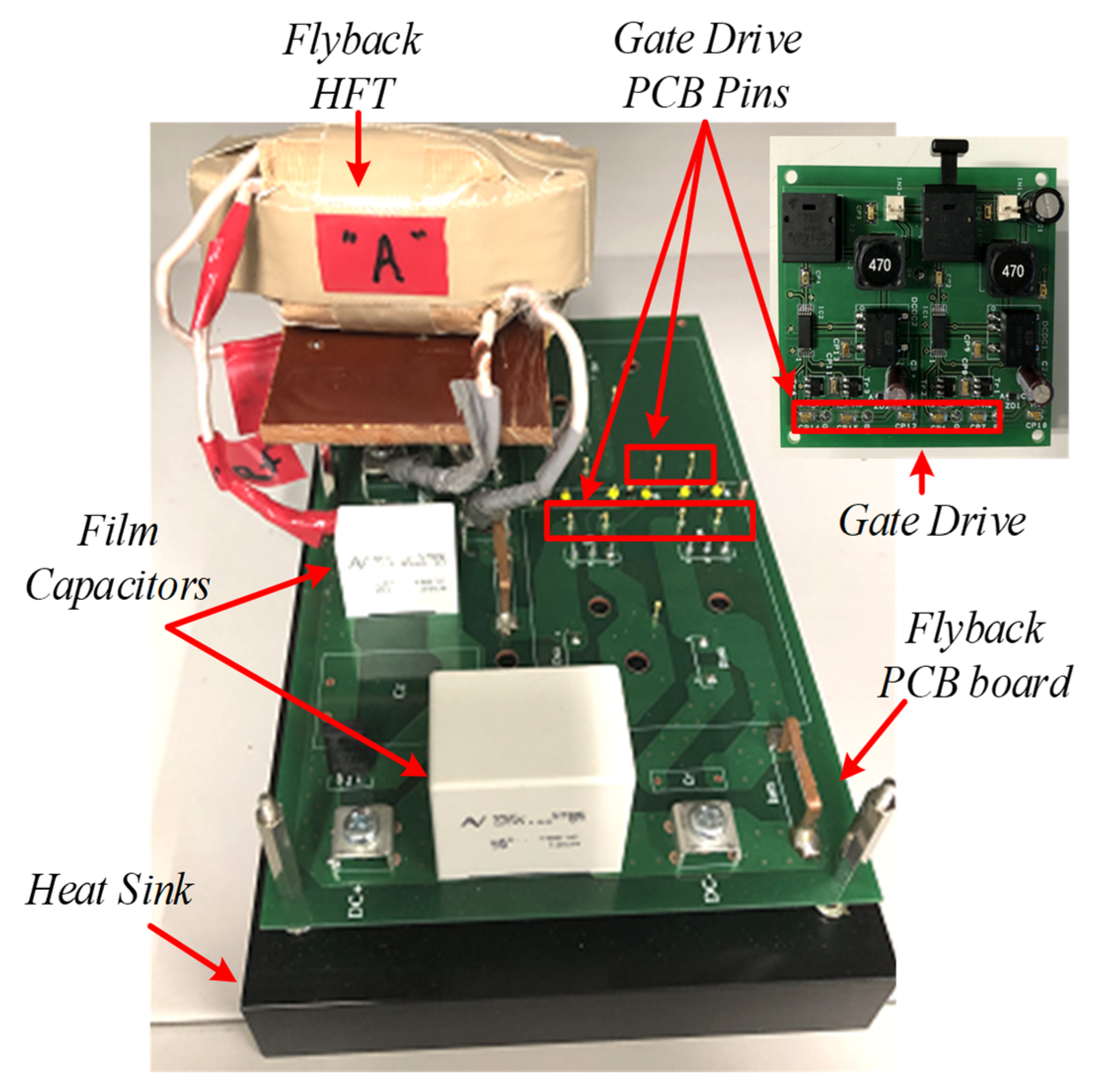
3.2. Hardware Implementation

Different outstanding magnetic materials are utilized for high frequency transformers/inductors design, such as monocrystalline, ferrite, nanocrystalline, amorphous, and powder magnetic materials. A comparison between these materials has been demonstrated in [38,39]. Soft ferrite materials are the common, low cost, and acceptable power loss in low power applications for micro-inverters power-level applications [39]. Thus, EER-94 soft ferrite core is used for the proposed converter module implementation. The core parameters are: Ae = 712 mm2 effective cross-section area, Ve = 158,000 mm3 effective volume, and permeability µ = 2500. In addition, LITZ wire has been used for HFT implementation for eddy current minimization to improve the system efficiency.
Recent isolated converters utilize a complicated magnetic structure that is composed of multiple heterogeneous elements (core material + air gap) and different winding layers. The terminal voltage of the proposed MFBDI is variable due to the variable duty cycle; therefore, the number of turns can be obtained as follows [38,39];
N = V p r i _ x ( m a x ) K v × B × A e × F S W
where,
Vpri_x(max)is the maximum primary voltage of the HFT,
Kv is waveform factor,
B is the flux density,
Ae the core cross section area.
Moreover, the length of the required air gap is set to 1.6 mm for rated power operation, which can be formulated as follows [39]:
l e = N 2 · μ o · A C o r e L m
where µo is the free space permeability and le is the air-gap length.
Based on (24), the required number of turns for EER soft-ferrite core is 10, which is increased to 15 to maintain the required inductance when the air gap is included. Figure 9 show the PCB board of a single flyback module with the designed elements and power switches.

3.3. Input LC Filter Design

A single second-order LC low pass filter is used at the inverter input side for continuous DC input current with input ripples alleviation for renewable energy applications. The input filter is designed at a resonating frequency of fo, which can be expressed as [37];
f o = 1 2 π · L i n C i n
where the resonating frequency must follow the following expression:
10 f g f o f s w 10
Therefore, fo is selected as 4 kHz in which the input filter inductance and capacitance are 150 µH and 10 µF, respectively.

4. MFBDI Control Scheme

As earlier discussed, the flyback modules are controlled over a wide-range of duty-cycle variation to shape the modulus of sinusoidal voltage waveform with 120° phase-shift between the modules of different phases. Based on (2) and (3), assuming lossless operation of the proposed inverter, and by applying power balance of each phase of MFBDI, the instantaneous grid-powers (pu, pv, and pw) can be expressed as follows:
p u = 2 E s u i s u s i n 2 ( ω t + α )
p v = 2 E s v i s v s i n 2 ( ω t + α 2 π 3 )
p w = 2 E s w i s w s i n 2 ( ω t + α + 2 π 3 )
Moreover, the input power to each module can be expressed as follows:
p x = v i n i i n , m x ( t )
where m = (1, …, N), x = (u, v, w)
By applying power balance, therefore, the input currents can be formulated as follows:
i m u ( t ) = 2 E s u i s u v i n s i n 2 ( ω t + α )
i m v ( t ) = 2 E s v i s v v i n s i n 2 ( ω t + α 2 π 3 )
i m w ( t ) = 2 E s w i s w v i n s i n 2 ( ω t + α + 2 π 3 )
where (Esu, Esv, Esw) and (isu, isv, isw) are the grid RMS voltages and currents, respectively.
Based on the former equations, the input current for each module has a squared sinusoidal waveform due to the virtual unfolding stage offered by the differential connection at the grid side. Thus, the reference input currents for the proposed MFBDI can be formulated as follows:
i m u ( t ) = 2 E s u v i n I s u s i n 2 ( ω t + α )
i m v = 2 E s v v i n I s v s i n 2 ( ω t + α 2 π 3 )
i m w = 2 E s w v i n I s w s i n 2 ( ω t + α + 2 π 3 )
where Isu, Isv, and Isw are peak values of grid-injected currents that can be decided by the PV MPPT technique in solar PV applications. In addition, the constant in these equations is used as
H x = 2 E s x v i n I s x
Based on the control-to-output transfer function of the flyback converter, the flyback module has a right half-plane zero (RHPZ) that affects the inverter stability during the inverter operation over a wide-range of duty-cycle variation [37]. Therefore, an accurate dynamic model is very important. Thus, the control-to-output transfer function of the flyback module can be expressed as follows [34,37];
G v d x ( s ) = v o x ( s ) d x ( s ) = G 0 · b 0 + b 1 S + b 2 S 2 + b 3 S 3 a 0 + a 1 S + a 2 S 2 + a 3 S 3
where G0 is the DC gain, (b0b3) are constants decides the zero locations, and (a1a3) are the constants of poles locations, which are formulated in Table 4 based on the system parameters.
Therefore, a robust designed compensator is required to maintain the inverter stability over a wide-range of duty-cycle and frequency variations. Considering the order of the proposed MFBDI transfer function, a Type-II compensator is used to stabilize the system, where its transfer function can be expressed as follows [40]:
G c x ( s ) = G c 0 · ( 1 + S ω z 1 ) ( 1 + S ω p 1 ) · ( 1 + S ω p 2 )
where G c 0 is compensator open-loop gain,
ω z 1 ,   ω p 1 ,   and   ω p 2 are frequency locations of converter zeros and poles, respectively.
The compensator static gain, Gc0, boosts the DC-gain of the converter open-loop transfer function, which enhances the controller steady state error. In addition, the compensator PID zero (ωz1) improves the flyback converter phase-margin (PM) that enhances the system stability and stretches its bandwidth. Moreover, the two poles of the PID compensator are located, one at low-frequency (ωp1), and the other at high-frequency close to switching frequency (ωp2). The low-frequency pole flattens the converter DC-gain that improves the controller accuracy; however, high-frequency pole eliminates the high-frequency oscillations and damps the converter switching harmonics.
In addition, the mismatch between the flyback modules flows circulating power between converter modules, which results in the SOHC in the grid-injected currents as illustrated in (15) and (16). Therefore, the proposed control strategy comprises two control loops; the main and secondary control loops. The main control loop regulates the grid currents by controlling the converter three-phase primary currents: however, the secondary control loop eliminates the negative sequence SOHC for sinusoidal grid injected currents. Low-pass filter (LPF), triggered at (−2ω), is used for SOHC mitigation in the secondary control-loop. The three-phase grid currents are sensed in which SOHCs are extracted using LPFs, and consequently eradicated from the grid currents. The LPF transfer function as be expressed as follows:
G s ( s ) = 1 ( 1 + S ω n )
The closed-loop control scheme of the proposed MFBDI for grid-integrated operation is portrayed in Figure 10. Moreover, the overall open-loop transfer function of the converter can be expressed as follows [37]:
T ( s ) = G v d x ( s ) · G l g x ( s ) · G c 1 x ( s ) · G p w m ( s ) · H s x ( s ) · G S L S ( s )
where T(s) is open-loop transfer function,
Gvdx(s) is control-to-output transfer function,
Glgx(s) is grid filter transfer function,
Gc1x(s) is compensator transfer function considering LPF,
Gpwm(s) is modulator transfer function,
Hsx(s) is sensor transfer function,
GSLS(s) is static linearization strategy of converter duty cycle.
In addition, the static linearized duty cycle of the proposed flyback module can be expressed, based on (10), as follows:
G S L S x ( s ) = m ( s ) · ( 1 + K x ) m ( s ) · ( 1 + K x ) + 1
where m(s) is the compensator’s output signals or static gain of the small-signal component of the differential converter.
Moreover, the bode plot of the inverter transfer function, considering the LPF, is depicted in Figure 11 using MATLAB/Simulink software. The proposed compensator stabilizes the MFBDI over the wide-range of duty cycle variations. Considering the proposed control strategy, the converter closed-loop transfer function DC-gain and bandwidth are 91 dB and 700 Hz, respectively. In addition, the converter phase margin is 36 degrees, which confirms converter stability over a wide-range of duty cycle and frequency variations.

5. System Verification

5.1. Simulation Results

The proposed MFBDI is verified by using PSIM simulation software of 5 kW modular flyback differential inverter architecture considering three paralleled flyback modules in each phase. The simulation parameters of the proposed MFBDI are listed in Table 5. Figure 12 shows the simulation results of the grid integrated MFBDI with and without the SOHC compensation strategy. In both cases, the waveforms of the proposed converter are depicted as follows: duty cycles (du, dv, dw), grid voltages (vsu, vsv, vsw), grid currents (isu, isv, isw), u-phase currents (isu, isu1, isu2, isu3), and d-q axis currents (id,ref, id,act.). The grid injected currents have a high SOHC, which increases the THD of the grid currents. With the proposed LPF-based compensation strategy, the MFBDI supplies the grid with sinusoidal current waveforms with low contained THD. It is worth mentioning that in both cases, the proposed control algorithm manages the power-sharing between the parallel modules for high power applications.
In addition, a 15% mismatch between the parameters of the flyback parallel modules of (u-phase) to investigate the proposed converter operation during parameters divergence. The u-phase parameters mismatch is considered according to Table 6. Figure 13 shows the system results considering the parameters mismatch. Figure 13a shows the waveforms of duty cycles, grid voltages, grid currents, primary currents, output voltages, and the input DC voltage and current to confirm the system stable operation during the circuit parameters mismatch. Moreover, the input current ripples are alleviated for continuous input current operation for renewable energy applications. In addition, Figure 13b depicts zoomed region of the system results to illustrate the parameters mismatch effects on the primary currents, grid currents, and output voltages of phase (u). Clearly, the converter has small deviations between the primary currents, grid supplied currents, and output voltages waveforms, which have a negligible effect on the converter overall operation.

5.2. Experimental Results

In order to validate the proposed three-phase MFBDI, a single module/phase experimental system prototype was carried out for the proposed DFBDI. Hence, the proposed system was validated via a single module/phase 1.6 W, 200 V, and 50 kHz switching frequency experimental prototype. The system prototype photograph is depicted in Figure 14. The system prototype considers three flyback modules utilizing a single module in each phase. SiC MOSFETs (C2M0040120D) are used for the converter switches in the experimental system, which decrease the system losses and improves the system overall efficiency. In addition, a simple robust designed RC snubber-circuit was designed according to [37] for voltage spikes mitigation due to the existence of the HFT leakage inductance. Moreover, the proposed MFBDI is controlled experimentally using a DSP (TMS320C6713A, TI) digital controller. The proposed system experimental parameters are listed in Table 7. The MFBDI experimental results were captured from the screen of a Yokogawa DL850E digital oscilloscope considering two operating conditions; without and with SOHC compensation. In both cases, the captured experimental waveforms are arranged as follows: three-phase grid voltages, grid currents, output voltages, input DC voltage, and input DC current, respectively. Without SOHC compensation, Figure 15 shows the input and output waveforms of the proposed MFBDI. Clearly, the grid currents are distorted by high SOHC of 51%, which matches the former simulation results, which increases the grid current THD to 36% that exceeds the IEEE and IEC harmonic standard limits. In addition, the SOHC in the grid currents distorts the converter input DC current with a third harmonic order as clearly portrayed in Figure 15, which is important for renewable energy applications such as solar PV and fuel cells. On the other hand, the converter experimental results after the harmonic elimination strategy are depicted Figure 16. With the help of the harmonic compensation strategy, the SOHC was eliminated from the grid-injected currents and the SOHC was reduced to 0.82%, as shown in Figure 16b. Thus, the grid-injected currents are almost sinusoidal waveforms with a THD of 4.6%, which matches IEEE and IEC harmonic standard limits. Moreover, the SOHC compensation strategy eliminates the third order harmonic component from the DC input current, as depicted in Figure 16a, which is important for solar PV applications. Moreover, the single LC input filter mitigates input current ripples, which offers an important feature for renewable energy applications. It worth mentioning that the voltage stress of the converter components is within the designed region due to the robust designed snubber circuit.
In addition, the harmonic orders of the grid injected currents are compared with the IEC 63000-3-2(Class-A) harmonic standard, as depicted in Figure 17. Obviously, the grid current harmonic orders are within the acceptable limit up to the 15th order, which confirms the operation of the SOHC compensation loop in the system control scheme. Finally, the proposed converter efficiency profile was analyzed considering a single flyback DC-DC module operation from the proposed MFBDI between (75 and 600 W) as depicted in Figure 18. Obviously, the converter efficiency is low for low-power operation due to the system conduction loss. However, the system efficiency enhances with increasing the power processed by the proposed converter to reach its optimal value and start to decrease again as depicted in the converter efficiency profile portrayed in Figure 18.

6. Conclusions

A modular single-stage three-phase differential inverter is presented in this paper based on the flyback DC-DC module. The proposed converter is verified via three-parallel flyback modules for 5 kW power rating for renewable energy applications. A detailed mathematical model of the proposed MFBDI confirming the SOHC is provided in this paper. Module parameters design strategy are illustrated for acceptable voltage and current ripples. In addition, a new control scheme based-on flyback primary current detection is used to control the grid integrated operation. Two control loops are used in the proposed control scheme for grid currents regulation (loop-1) and SOHC compensation (loop-2), respectively. To ensure the modular operation of the proposed converter architecture, 15% parameters mismatch is applied between the parallel flyback modules to confirm the modular operation of the MFBDI over flyback modules divergence. For experimental validation of the MFBDI, a laboratory prototype based 1.6 W/200 V was built and the experimental results of the proposed converter without and with the LPF-based harmonic elimination strategy are carried out. Clearly, the experimental results follow the simulation results that confirms the robust design of the converter. Moreover, the grid current harmonic orders are compared with the IEC61000-3-2 (Class-A), which are within the standard permissible limit. Furthermore, the converter efficiency profile is analyzed at different power levels.

Author Contributions

Conceptualization, A.I.M.A.; methodology, A.I.M.A. and T.T.; software, A.I.M.A., T.T. and M.A.S.; validation, A.I.M.A., T.T. and M.A.S.; formal analysis, A.I.M.A., and Z.M.A.; investigation, A.I.M.A.; resources A.I.M.A., T.T., M.A.S., Z.M.A. and C.A.T.; data curation, A.I.M.A.; writing—original draft preparation, A.I.M.A. All authors have read and agreed to the published version of the manuscript.

Funding

This research received no external funding.

Institutional Review Board Statement

Not applicable.

Informed Consent Statement

Not applicable.

Data Availability Statement

Not applicable.

Conflicts of Interest

The authors declare no conflict of interest.

References

  1. Carrasco, J.M.; Franquelo, L.G.; Bialasiewicz, J.T.; Galvan, E.; PortilloGuisado, R.; Prats, M.A.M.; Leon, J.I.; Moreno-Alfonso, N. Power-Electronic Systems for the Grid Integration of Renewable Energy Sources: A Survey. IEEE Trans. Ind. Electron. 2006, 53, 1002–1016. [Google Scholar] [CrossRef]
  2. Darwish, A.; Alotaibi, S.; Elgenedy, M.A. Current-Source Single-Phase Module Integrated Inverters for PV Grid-Connected Applications. IEEE Access 2020, 8, 53082–53096. [Google Scholar] [CrossRef]
  3. Ali, A.I.M.; Mohamed, H.R.A. Improved P&O MPPT algorithm with efficient open-circuit voltage estimation for two-stage grid-integrated PV system under realistic solar radiation. Int. J. Electr. Power Energy Syst. 2021, 137, 107805. [Google Scholar] [CrossRef]
  4. Lodh, T.; Pragallapati, N.; Agarwal, V. Novel Control Scheme for an Interleaved Flyback Converter Based Solar PV Microinverter to Achieve High Efficiency. IEEE Trans. Ind. Appl. 2018, 54, 3473–3482. [Google Scholar] [CrossRef]
  5. Bana, P.R.; Panda, K.P.; Naayagi, R.T.; Siano, P.; Panda, G. Recently Developed Reduced Switch Multilevel Inverter for Renewable Energy Integration and Drives Application: Topologies, Comprehensive Analysis and Comparative Evaluation. IEEE Access 2019, 7, 54888–54909. [Google Scholar] [CrossRef]
  6. Ali, A.I.M.; Sayed, M.A.; Takeshita, T. Isolated single-phase single-stage DC-AC cascaded transformer-based multilevel inverter for stand-alone and grid-tied applications. Int. J. Electr. Power Energy Syst. 2021, 125, 106534. [Google Scholar] [CrossRef]
  7. Taghvaie, A.; Haque, M.E.; Saha, S.; Mahmud, M.A. A new step-up switched-capacitor voltage balancing converter for NPC multilevel inverter-based solar PV system. IEEE Access 2020, 8, 83940–83952. [Google Scholar] [CrossRef]
  8. Ali, A.I.M.; Sayed, M.A.; Takeshita, T.; Hassan, A.M.M.; Azmy, A.M. A single-phase modular multilevel inverter based on controlled DC-cells under two SPWM techniques for renewable energy applications. Int. Trans. Electr. Energy Syst. 2020, 31, 12599. [Google Scholar] [CrossRef]
  9. Jain, S.; Agarwal, V. A Single-Stage Grid Connected Inverter Topology for Solar PV Systems with Maximum Power Point Tracking. IEEE Trans. Power Electron. 2007, 22, 1928–1940. [Google Scholar] [CrossRef] [Green Version]
  10. Liang, T.; Kuo, Y.; Chen, J. Single-stage photovoltaic energy conversion system. IEE Proc. Electr. Power Appl. 2001, 148, 339–344. [Google Scholar] [CrossRef]
  11. Gangavarapu, S.; Verma, M.; Rathore, A.K. A Novel Transformerless Single-Stage Grid-Connected Solar Inverter. IEEE J. Emerg. Sel. Top. Power Electron. 2020, 1. [Google Scholar] [CrossRef]
  12. Ali, A.; Sayed, M.; Mohamed, A. Seven-Level Inverter with Reduced Switches for PV System Supporting Home-Grid and EV Charger. Energies 2021, 14, 2718. [Google Scholar] [CrossRef]
  13. Guo, B.; Su, M.; Sun, Y.; Wang, H.; Liu, B.; Zhang, X.; Pou, J.; Yang, Y.; Davari, P. Optimization Design and Control of Single-Stage Single-Phase PV Inverters for MPPT Improvement. IEEE Trans. Power Electron. 2020, 35, 13000–13016. [Google Scholar] [CrossRef]
  14. Pomilio, J.A.; Spiazzi, G. High-precision current source using low-loss, single-switch, three-phase AC/DC converter. IEEE Trans. Power Electron. 1996, 11, 561–566. [Google Scholar] [CrossRef]
  15. Bhuvaneswari, G.; Singh, B.; Singh, S. Three-phase single stage medium power supply using Cuk converter. In Proceedings of the 2012 IEEE 5th India International Conference on Power Electronics (IICPE), Delhi, India, 6–8 December 2012; pp. 1–6. [Google Scholar]
  16. Davoodnezhad, R.; Holmes, D.G.; McGrath, B.P. A Novel Three-Level Hysteresis Current Regulation Strategy for Three-Phase Three-Level Inverters. IEEE Trans. Power Electron. 2013, 29, 6100–6109. [Google Scholar] [CrossRef]
  17. Ahmed, T.A.; Mohamed, E.E.; Youssef, A.-R.; Ibrahim, A.; Saeed, M.S.; Ali, A.I. Three phase modular multilevel inverter-based multi-terminal asymmetrical DC inputs for renewable energy applications. Eng. Sci. Technol. Int. J. 2020, 23, 831–839. [Google Scholar] [CrossRef]
  18. Saleem, M.W.; Choi, K.-Y.; Kim, R.-Y. Resonance damping for an LCL filter type grid-connected inverter with active disturbance rejection control under grid impedance uncertainty. Int. J. Electr. Power Energy Syst. 2019, 109, 444–454. [Google Scholar] [CrossRef]
  19. Saleem, M.; Ko, B.-S.; Kim, S.-I.; Chowdhry, B.S.; Kim, R.-Y. Active Disturbance Rejection Control Scheme for Reducing Mutual Current and Harmonics in Multi-Parallel Grid-Connected Inverters. Energies 2019, 12, 4363. [Google Scholar] [CrossRef] [Green Version]
  20. Zhang, Z.; He, X.-F.; Liu, Y.-F. An Optimal Control Method for Photovoltaic Grid-Tied-Interleaved Flyback Microinverters to Achieve High Efficiency in Wide Load Range. IEEE Trans. Power Electron. 2013, 28, 5074–5087. [Google Scholar] [CrossRef]
  21. Kouro, S.; Leon, J.I.; Vinnikov, D.; Franquelo, L.G. Grid-Connected Photovoltaic Systems: An Overview of Recent Research and Emerging PV Converter Technology. IEEE Ind. Electron. Mag. 2015, 9, 47–61. [Google Scholar] [CrossRef]
  22. Tamyurek, B.; Kirimer, B. An Interleaved High-Power Flyback Inverter for Photovoltaic Applications. IEEE Trans. Power Electron. 2015, 30, 3228–3241. [Google Scholar] [CrossRef]
  23. Zapata, J.W.; Kouro, S.; Carrasco, G.; Renaudineau, H.; Meynard, T. Analysis of Partial Power DC–DC Converters for Two-Stage Photovoltaic Systems. IEEE J. Emerg. Sel. Top. Power Electron. 2019, 7, 591–603. [Google Scholar] [CrossRef]
  24. Caceres, R.; Barbi, I. A boost DC-AC converter: Analysis, design, and experimentation. IEEE Trans. Power Electron. 1999, 14, 134–141. [Google Scholar] [CrossRef]
  25. Chen, D.; Wang, G. Differential Buck DC–DC Chopper Mode Inverters with High-Frequency Link. IEEE Trans. Power Electron. 2010, 26, 1444–1451. [Google Scholar] [CrossRef]
  26. Jang, M.; Ciobotaru, M.; Agelidis, V.G. A Single-Phase Grid-Connected Fuel Cell System Based on a Boost-Inverter. IEEE Trans. Power Electron. 2013, 28, 279–288. [Google Scholar] [CrossRef]
  27. Knight, J.; Shirsavar, S.; Holderbaum, W. An improved reliability cuk based solar inverter with sliding mode control. IEEE Trans. Power Electron. 2006, 21, 1107–1115. [Google Scholar] [CrossRef]
  28. Mazumder, S.K.; Mehrnami, S. A low-device-count single-stage direct-power-conversion solar microinverter for microgrid. In Proceedings of the 2012 3rd IEEE International Symposium on Power Electronics for Distributed Generation Systems (PEDG), Aalborg, Denmark, 25–28 June 2012; pp. 725–730. [Google Scholar]
  29. Kulkarni, A.; Gupta, A.; Mazumder, S.K. Resolving practical design issues in a single-phase grid-connected GaN-FET-based differential-mode inverter. IEEE Trans. Power Electron. 2017, 33, 3734–3751. [Google Scholar] [CrossRef]
  30. Darwish, A.; Holliday, D.; Ahmed, S.; Massoud, A.M.; Williams, B.W. A single-stage three-phase inverter based on Cuk converters for PV applications. IEEE J. Emerg. Sel. Top. Power Electron. 2014, 2, 797–807. [Google Scholar] [CrossRef]
  31. Darwish, A.; Elgenedy, M.A. Current-Source Modular Medium-Voltage Grid-Connected System with High-Frequency Isolation for Photovoltaic Applications. IEEE Trans. Energy Convers. 2018, 34, 255–266. [Google Scholar] [CrossRef] [Green Version]
  32. Diab, M.S.; Elserougi, A.; Massoud, A.M.; Abdel-Khalik, A.S.; Ahmed, S. A four-switch three-phase SEPIC-based inverter. IEEE Trans. Power Electron. 2014, 30, 4891–4905. [Google Scholar] [CrossRef]
  33. Mehrnami, S.; Mazumder, S.K.; Soni, H. Modulation Scheme for Three-Phase Differential-Mode Ćuk Inverter. IEEE Trans. Power Electron. 2016, 31, 2654–2668. [Google Scholar] [CrossRef]
  34. Darwish, A.; Massoud, A.; Holliday, D.; Ahmed, S.; Williams, B. Single-stage Three-phase Differential-mode Buck-Boost Inverters with Continuous Input Current for PV Applications. IEEE Trans. Power Electron. 2016, 31, 1. [Google Scholar] [CrossRef] [Green Version]
  35. Za’Im, R.; Jamaludin, J.; Rahim, N.A. Photovoltaic Flyback Microinverter with Tertiary Winding Current Sensing. IEEE Trans. Power Electron. 2019, 34, 7588–7602. [Google Scholar] [CrossRef]
  36. Li, Y.; Oruganti, R. A Low Cost Flyback CCM Inverter for AC Module Application. IEEE Trans. Power Electron. 2011, 27, 1295–1303. [Google Scholar] [CrossRef]
  37. Erickson, R.W.; Maksimovic, D. Fundamentals of Power Electronics; Springer Science & Business Media: Berlin, Germany, 2007. [Google Scholar]
  38. Blackburn, J.L. Symmetrical Components for Power Systems Engineering; CRC Press: Boca Raton, FL, USA, 2017. [Google Scholar]
  39. Aldosari, O.; Rodriguez, L.A.G.; Balda, J.C.; Mazumder, S.K. Design Trade-Offs for Medium- and High-Frequency Transformers for Isolated Power Converters in Distribution System Applications. In Proceedings of the 2018 9th IEEE International Symposium on Power Electronics for Distributed Generation Systems (PEDG), Charlotte, NC, USA, 25–28 June 2018; pp. 1–7. [Google Scholar]
  40. Demystifying Type II and Type III Compensators Using Opamp and OTA for DC/DC Converters. Available online: https://pdf4pro.com/view/demystifying-type-ii-and-type-iii-compensators-1507f1.html (accessed on 8 February 2014).
Figure 1. Circuit configuration of the single-stage three-phase MFBDI.
Sensors 22 02064 g001
Figure 2. One phase of the proposed MFBDI, N = 3.
Sensors 22 02064 g002
Figure 3. Control waveforms and current/voltage components.
Sensors 22 02064 g003
Figure 4. Single module bi-directional power flow of the proposed MFBDI.
Sensors 22 02064 g004
Figure 5. Temporarily power transfer of the MFBDI: (a) Energy storage in the HFT magnetizing inductance, (b) Energy release to supply the load and charging the output capacitor.
Sensors 22 02064 g005
Figure 6. Switching waveforms of single flyback module of the proposed MFBDI.
Sensors 22 02064 g006
Figure 7. Flyback converter voltage gain.
Sensors 22 02064 g007
Figure 8. Averaged one-cycle of the proposed MFBDI.
Sensors 22 02064 g008
Figure 9. PCB board of a flyback converter module.
Sensors 22 02064 g009
Figure 10. Control block diagram of the proposed MFBDI.
Sensors 22 02064 g010
Figure 11. Bode plot of the proposed control scheme of MFBDI.
Sensors 22 02064 g011
Figure 12. Simulation results of the proposed MFBDI at 5 kW; (a) with SOHC, (b) without SOHC.
Sensors 22 02064 g012
Figure 13. Simulation results of the proposed MFBDI at 5 kW considering 15% parameter mismatch. (a) Power frequency waveforms; (b) switching frequency waveforms.
Sensors 22 02064 g013
Figure 14. Experimental system prototype photograph.
Sensors 22 02064 g014
Figure 15. Experimental system results without SOHC compensation. (a) Converter results without SOHC compensation. (b) Grid current FFT harmonic spectrum without SOHC compensation.
Sensors 22 02064 g015
Figure 16. Experimental system results with SOHC compensation. (a) Converter results with SOHC compensation. (b) Grid current FFT harmonic spectrum with SOHC compensation.
Sensors 22 02064 g016
Figure 17. Grid current harmonic orders vs. IEC61000-3-2 (Class-A).
Sensors 22 02064 g017
Figure 18. Efficiency profile of a single flyback module of the proposed MFBDI.
Sensors 22 02064 g018
Table 1. Comparison study for MFBDI with its counterpart topologies.
Control/Ref.[29][33][34][35]Proposed
Switch No.46656
Diodes No.46640
Inductor No.79641
Capacitor No.69034
Modulation schemeDMSDMSCMSCMSCMS
No. of loops53322
ControllerPRNAPRHysteresisPI
FSW (kHz)1001252512050
THD (%)441.21.94.5
No. of sensors77745
Power rating, W500
(Single-phase)
500
(Three-phase)
2500
(Three-phase)
210
(Single-phase)
1600
(Three-phase)
Switch rating(GS66508P)
650 V, 30 A
NA(IRG7PH50K10D)
1200 V, 90 A
FDP51N25
IPAW60R190CE
(C2M0040120D)
1200 V, 60 A
NA: Not Available.
Table 2. Voltage and current stresses.
ComponentVoltageCurrentRipple Component
Cinvin (VPV) C i n · d v i n d t n · d x · i x C o x · f s w
LMx (HFT) v o x n n·ix d x · v i n L m x · f s w
Coxvox i x · ( 1 ( 1 d x ) 1 ) d x · i x C i n · f s w
Primary switch
(S1or S2)
v i n + v o x n n · i x ( 1 d x ) d x · v i n L m x · f s w
Secondary switch
(S3or S4)
vox i x ( 1 d x ) d x · v i n L m x · f s w
where x = u, v, or w.
Table 3. Flyback converter parameters.
Input DC voltage, Vdc100 V
Input filter, Lin, Cin150 µH, 10 µF
Grid voltage (L.L), Vg200 V, 60 Hz
Grid filter, Lg4 mH
HFT magnetizing inductance, LMx115 µH
HFT leakage inductance, LLeakage2.25 µH
Output capacitor, COx12.8 µF
HFT turns ratio, n1:1
Switching Frequency, FSW50 kHz
Table 4. Transfer Function Parameters.
b 3 = C i n D L i n 2 L M V i n a 3 = C i n L i n ( 1 D ) 2 [ L i n L M + C o R e q ( L i n r L + L M R i n ) ]
b 2 = C i n D V i n [ ( L i n r L ) + ( L M R i n ) + L i n R e q ( 2 D ) ] a 2 = L i n ( 1 D ) 2 [ C i n L i n R e q ( 1 D ) 2 + C i n ( L i n r L + L M R i n ) + C o ( L M R e q + D 2 + C i n R e q R i n r L ) ]
b 1 = V i n [ D L i n ( D L i n + C i n R i n r L + L M )     C i n L M R e q r L ( 1 D ) 2 ] a 1 = L i n ( 1 D ) 2 [ L M + D 2 L i n + C i n R e q R i n ( 1 D ) 2 + C o R e q ( R i n D 2 + r L ) ]
b 0 = V i n [ R e q ( 1 D ) 2 D ( D R i n + r L ) ] a 0 = ( 1 D ) 2 [ R e q ( 1 D ) 2 + r L + R i n D 2 ) ]
where LM is the HFT magnetizing inductance, Co or Cout is the flyback module output inductance, Req is the grid equivalent resistance, Rin is the resistance of the input inductor, rL is the resistance of the HFT magnetizing inductor.
Table 5. Simulation parameters of the MFBDI.
Rated inverter power, P5 kW
Input DC voltage, Vdc100 V
Input filter, Lin, Cin150 µH, 10 µF
Input filter resistance, rin2 Ω
Grid voltage (L.L), E, ω200 V, 2 × π × 60 rad/s
HFT magnetizing inductance, LMx115 µH
HFT primary resistance, rM50 mΩ
Output capacitor, COx12.8 µF
HFT leakage inductance, LLeakage2.25 µH
HFT turns ratio, n1:1
Grid filter, Lg4 mH
Grid inductor resistance, rg,25 mΩ
Switching Frequency, FSW50 kHz
PI controller gains, KP, KI0.097 A/V, 280 rad/s
Table 6. Parameter mismatch of the proposed MFBDI.
ElementDivergence
Values
Average
Current/Voltage
Mismatch
Percentage
HFT Magnetizing inductanceLM(u1) = 115 µH21 A3.57% (0.75 A)
LM(u2) = 132.25 µH21.75 A
LM(u3) = 97.75 µH20.25 A
HFT Leakage inductanceLLK(u1) = 2 µH21 A3.57% (0.75 A)
LLK(u2) = 2.3 µH21.75 A
LLK(u3) = 1.7 µH20.25 A
Output capacitorCo(u1) = 12.8 µH163.3 V0.6124% (1 V)
Co(u2) = 14.72 µH164.3 V
Co(u3) = 10.88 µH162.3 V
Table 7. Experimental parameters of the MFBDI.
Rated inverter power, P1650 kW
Input DC voltage, Vdc100 V
Input filter, Lin, Cin152.3 µH, 10 µF
Input filter resistance, rin1.5 Ω
Grid voltage (L.L), E, ω200 V, 2 × π × 60 rad/s
HFT magnetizing inductance, LMx115.52 µH
HFT primary resistance, rm50 mΩ
Output capacitor, COx12 µF
HFT leakage inductance, LLeakage2.56 µH
HFT turns ratio, n1:1
Grid filter, Lg4 mH
Grid inductor resistance, rg,25 mΩ
Switching Frequency, FSW50 kHz
PI controller gains, KP, KI0.097 A/V, 280 rad/s
Publisher’s Note: MDPI stays neutral with regard to jurisdictional claims in published maps and institutional affiliations.

