

Design of Precision-Aware Subthreshold-Based MOSFET Voltage Reference


Abstract
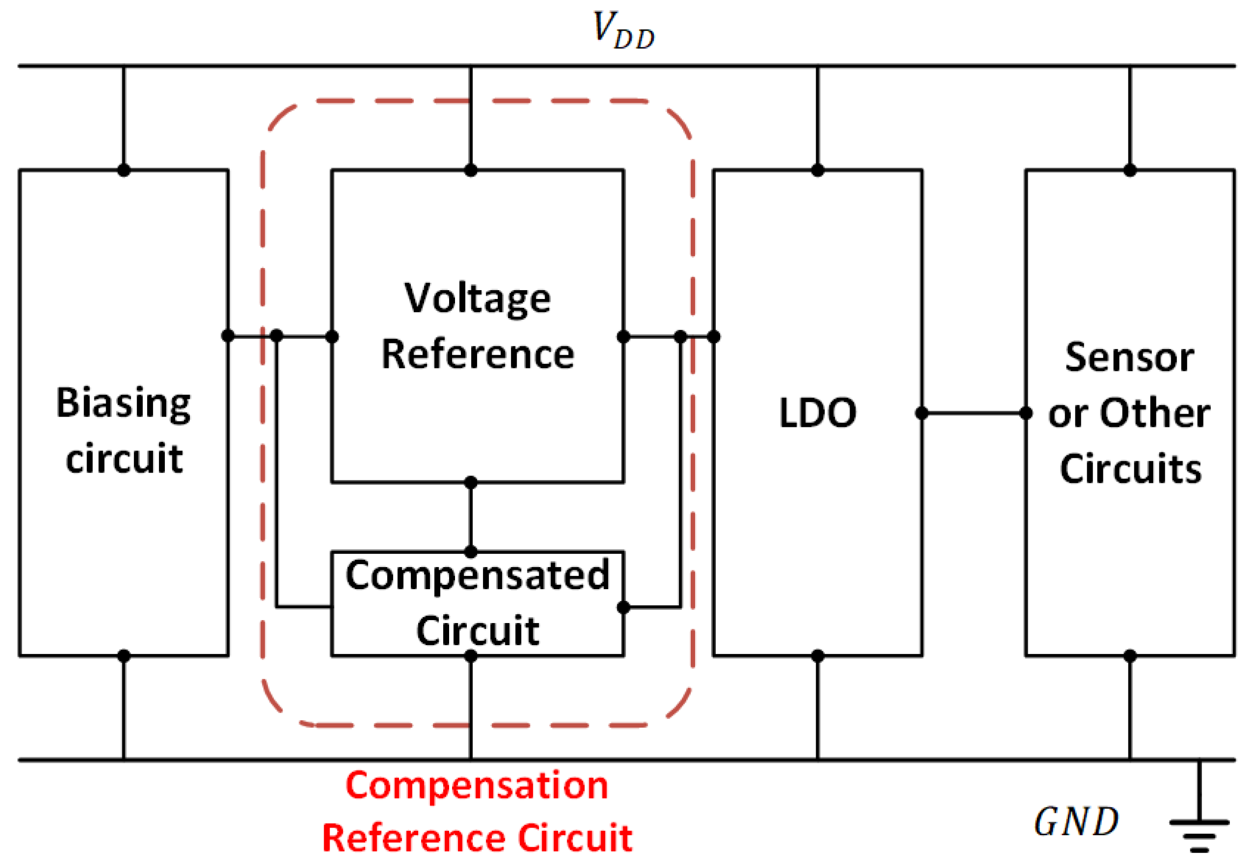
:1. Introduction
2. Representative Voltage References
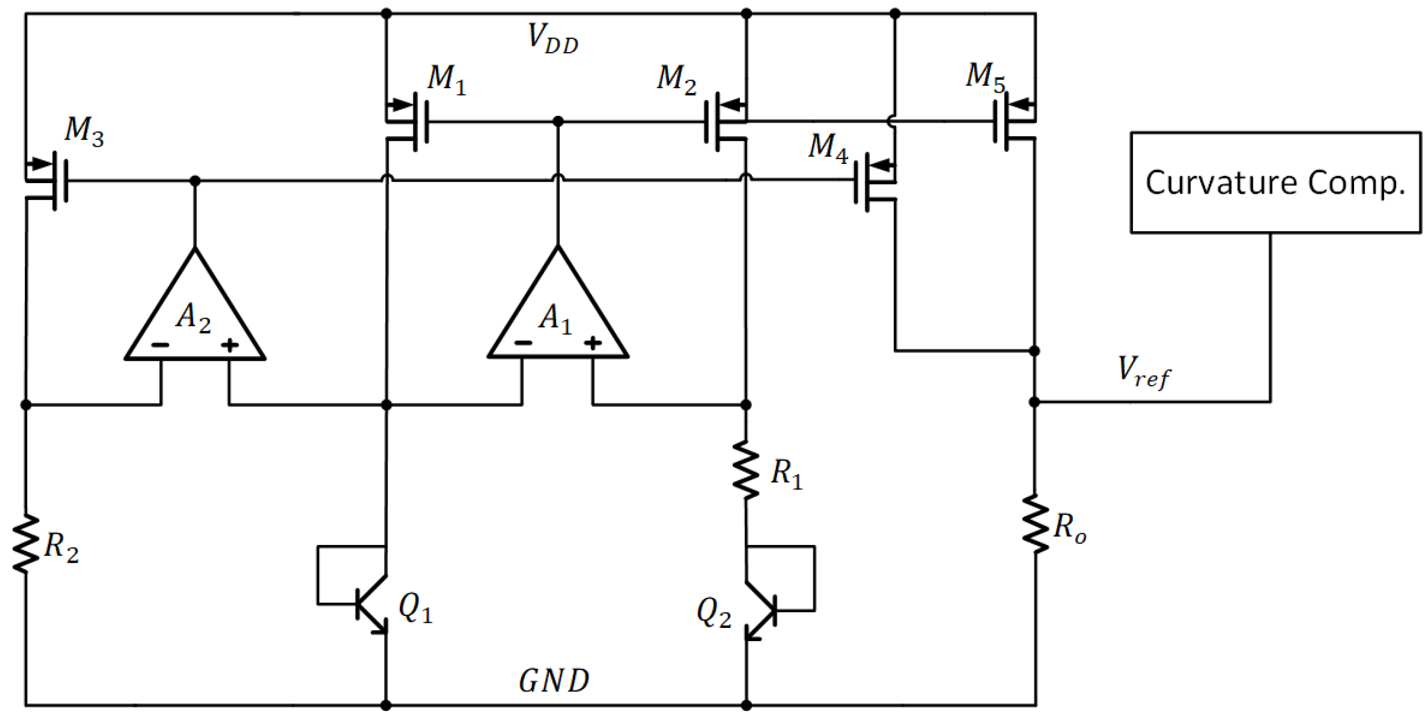
3. Proposed Second-Order Temperature Compensated Voltage Reference
3.1. Temperature Compensation of Proposed Voltage Reference

3.2. Analysis of Proposed Voltage Reference
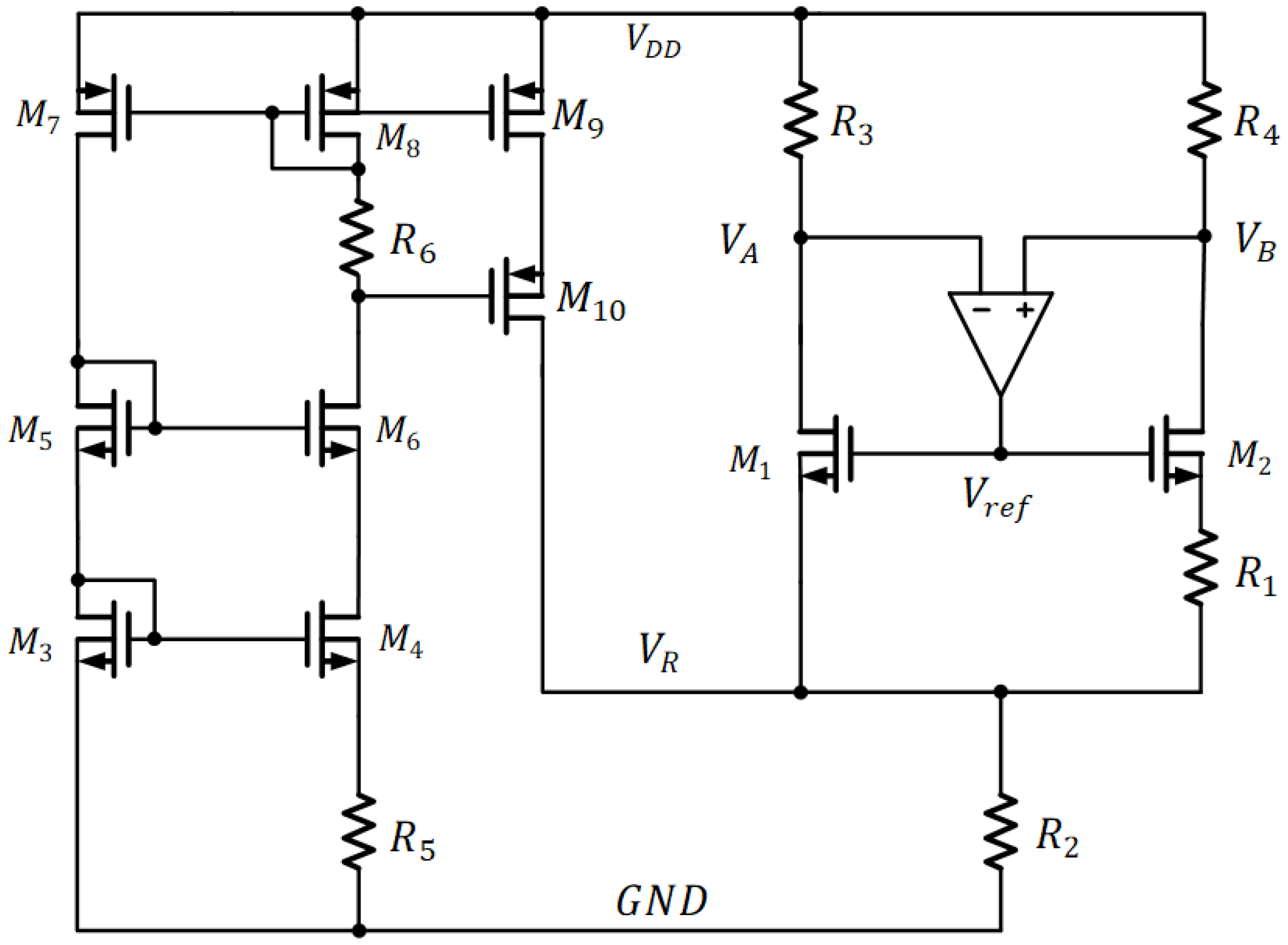
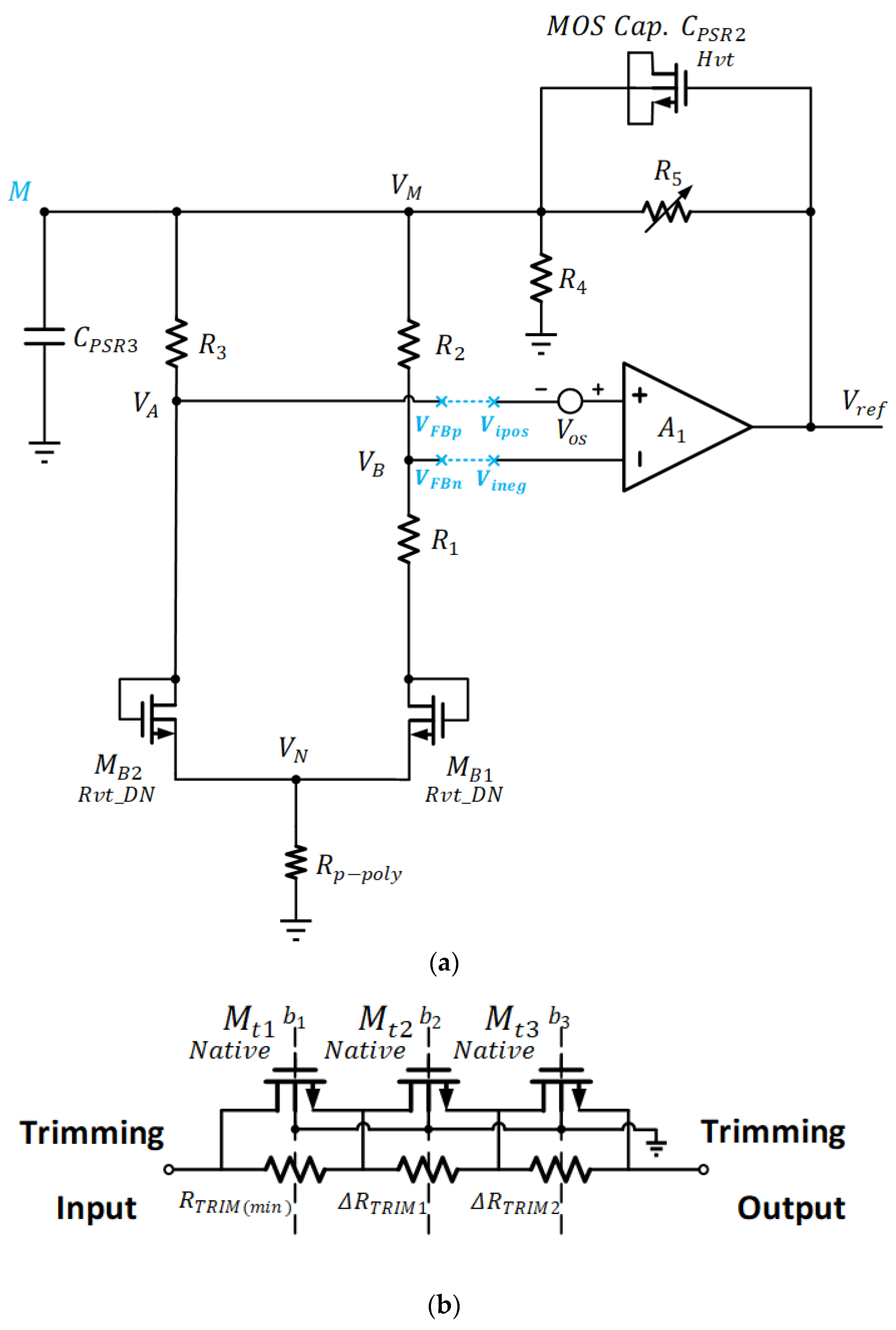
3.2.1. Core Circuit of Operational Amplifier
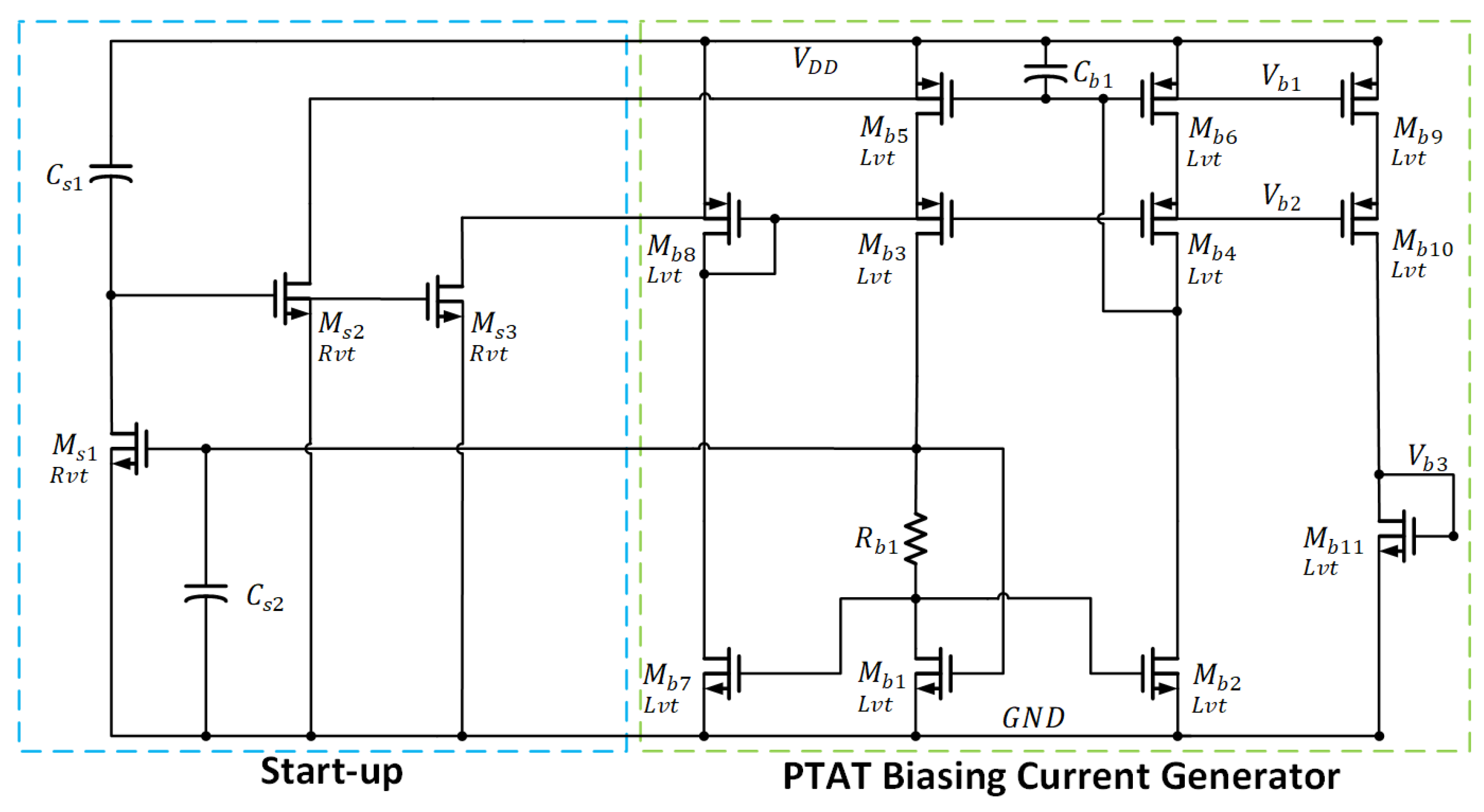
3.2.2. Basing Circuit of Operational Amplifier
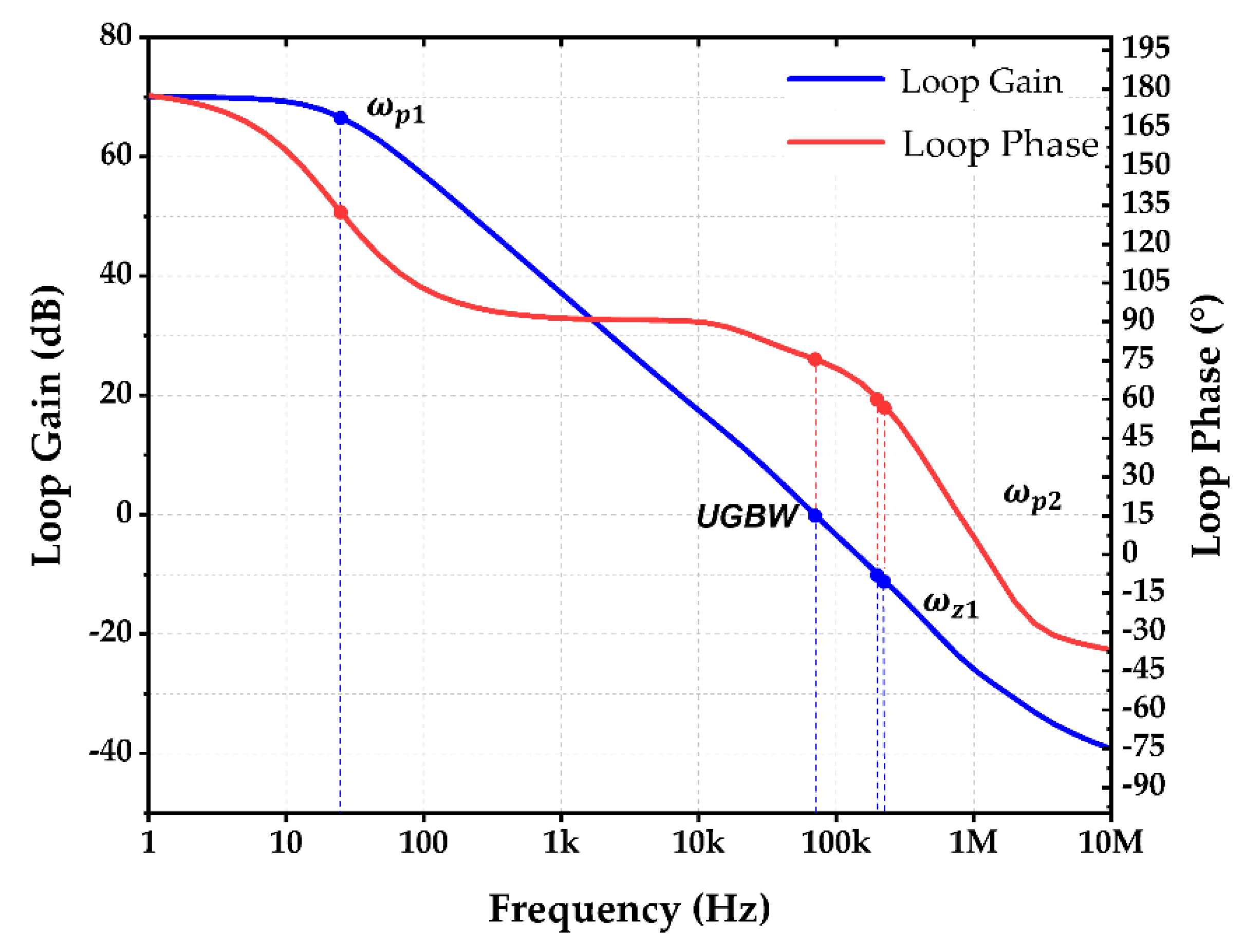
3.2.3. Frequency-Dependent Loop Gain Analysis of Voltage Reference
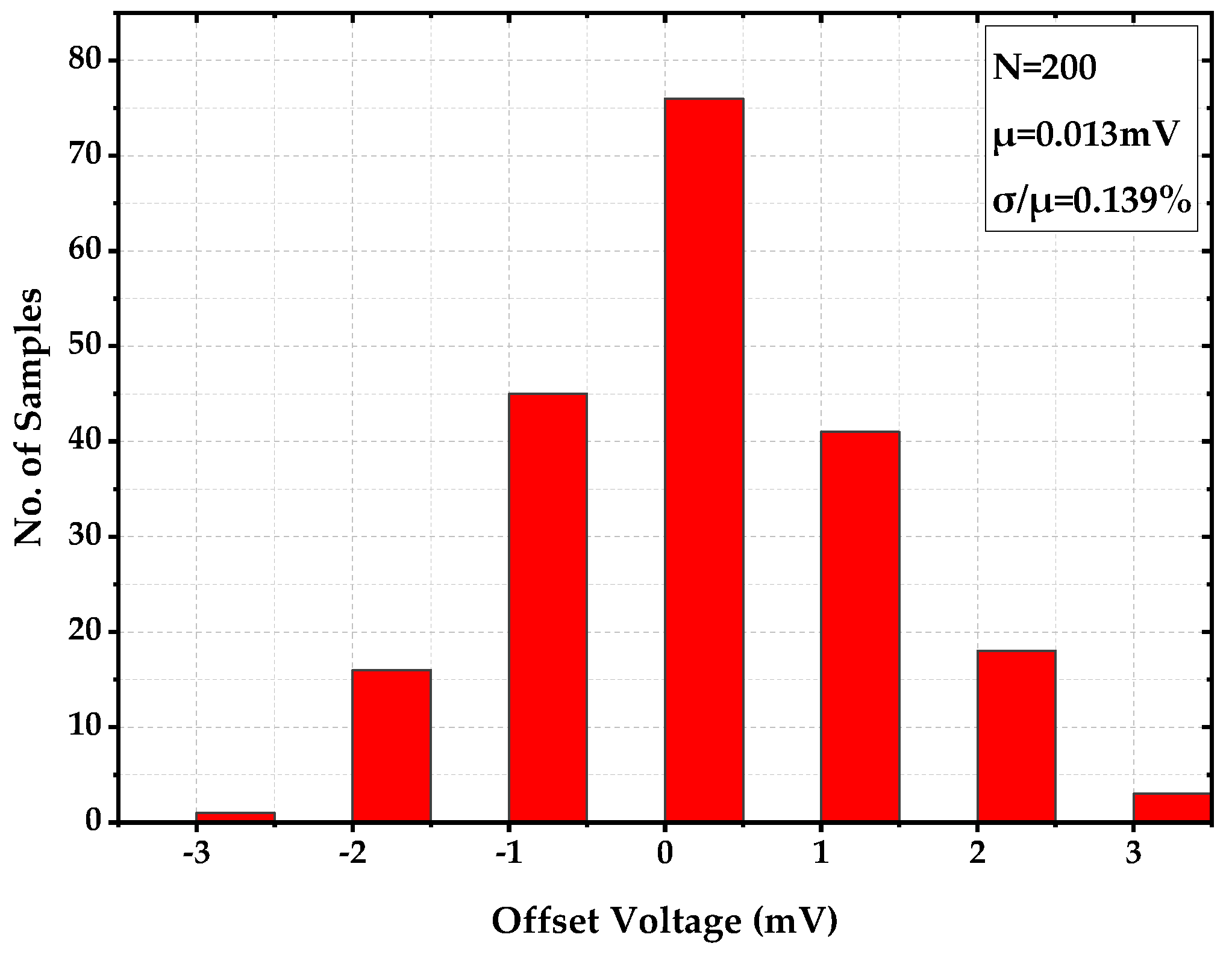
3.3. Offset Effect in Voltage Reference
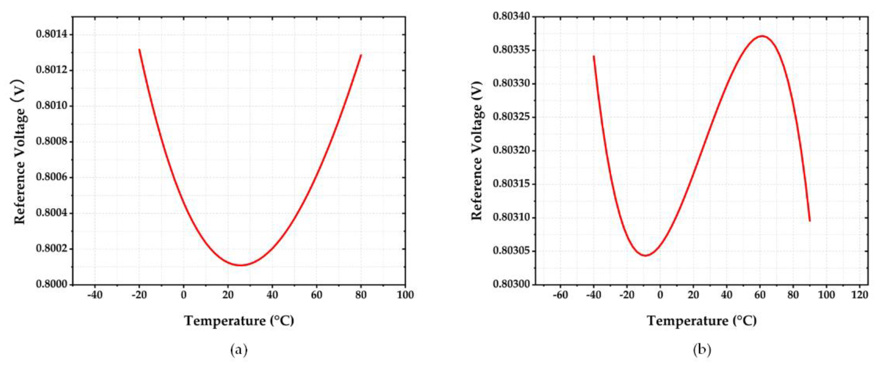
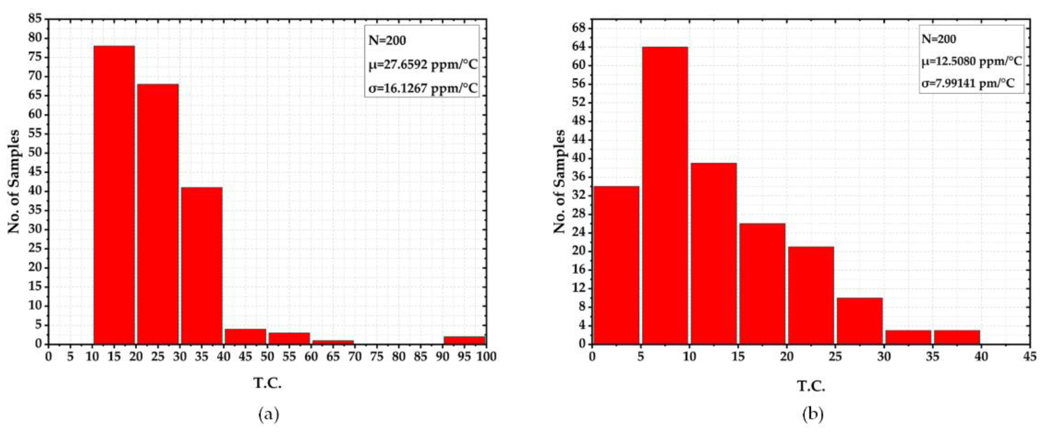
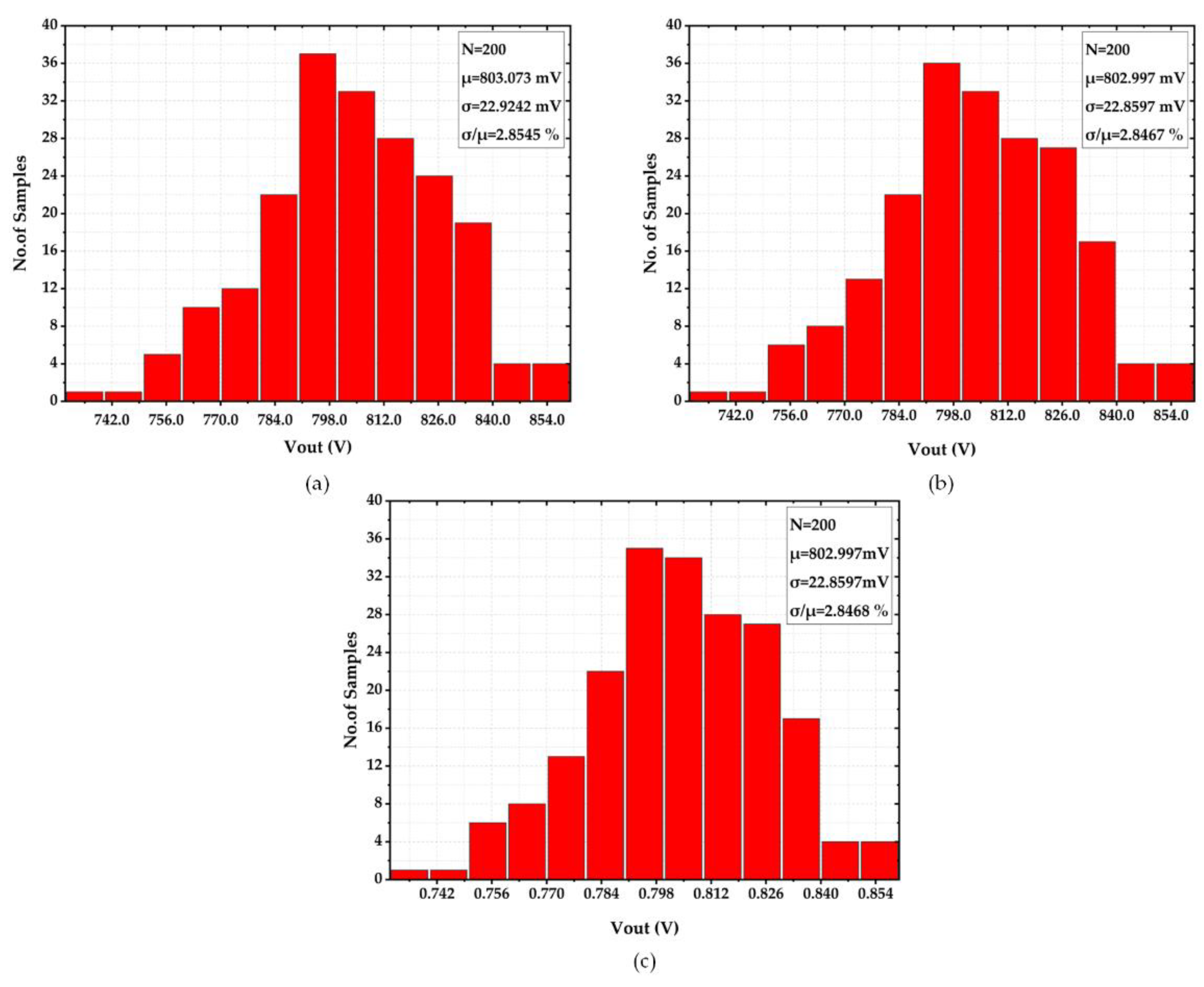
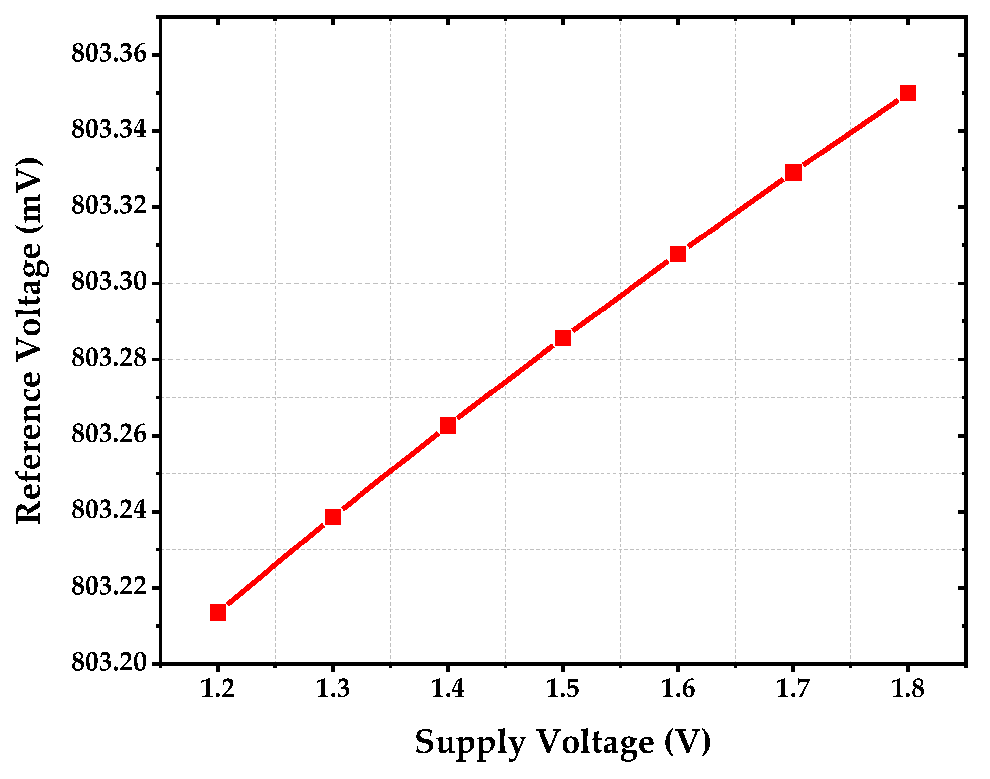
4. Results and Discussions
- Table 5 and Table 6 compare the performance of the proposed work with other representative reported works that include both types of parasitic BJT and sub-threshold MOSFET voltage references. Besides, a Figure-of-Merit (FOM) [26] performance metric was also utilized for evaluating the total PVT sensitivity of each voltage reference output. It is defined as follows:
- The process sensitivity pertains to the % output change due to process variation, the line sensitivity pertains to the % output change due to supply variation, and the T.C. of pertains to the % output change due to temperature variation. The lower value of FOM indicates low sensitivity of the reference circuit output.
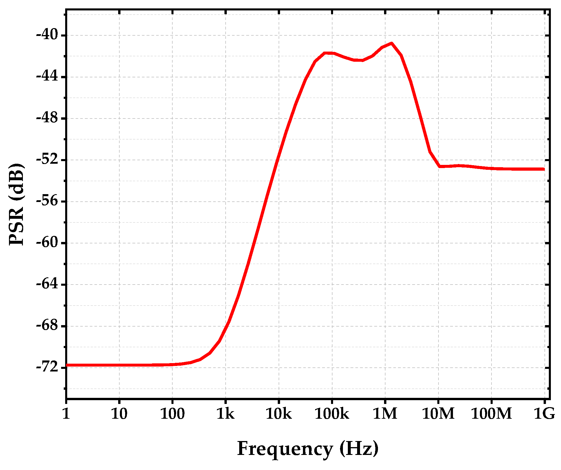
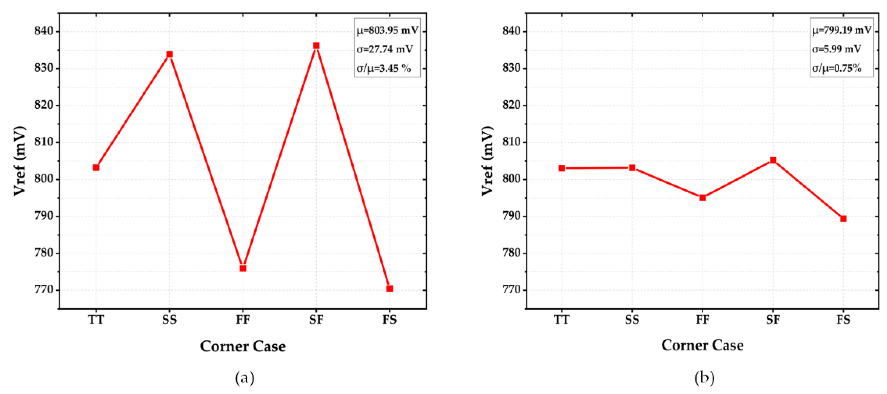
- When referring to the performance comparison of the BJT-based voltage references in Table 5, it can be seen that the proposed work offers slightly higher process sensitivity with respect to [6,21] but lower than [20] under no trimming condition. When trimmed, the proposed work offers comparable accuracy. Except for [6], it consumes lower power when compared with the majority of designs. However, the T.C. sensitivity obtained from the Monte-Carlo simulation is smaller than that of [6,20]. Regarding line sensitivity and low-frequency PSR, the obtained values are reasonably good. It is worth noting that the high-frequency PSR is very good in this work.
5. Conclusions
Author Contributions
Funding
Institutional Review Board Statement
Informed Consent Statement
Data Availability Statement
Conflicts of Interest
References
- Duan, Q.; Roh, J. A 1.2-V 4.2- ppm/°C High-Order Curvature-Compensated CMOS Bandgap Reference. IEEE Trans. Circuits Syst. I Regul. Pap. 2015, 62, 662–670. [Google Scholar] [CrossRef]
- Kamath, U.; Cullen, E.; Jennings, J.; Cical, I.; Walsh, D.; Lim, P.; Farley, B.; Staszewski, R. A 1-V Bandgap Reference in 7-nm FinFET with a Programmable Temperature Coefficient and Inaccuracy of ±0.2% From −45 °C to 125 °C. IEEE J. Solid-State Circuits 2019, 54, 1830–1840. [Google Scholar] [CrossRef]
- Liu, L.; Liao, X.; Mu, J. A 3.6 μVrms Noise, 3 ppm/°C TC Bandgap Reference with Offset/Noise Suppression and Five-Piece Linear Compensation. IEEE Trans. Circuits Syst. I Regul. Pap. 2019, 66, 3786–3796. [Google Scholar] [CrossRef]
- Lee, C.C.; Chen, H.M.; Lu, C.C.; Lee, B.Y.; Huang, H.C.; Fu, H.S.; Lin, Y.X. A High-Precision Bandgap Reference with a V-Curve Correction Circuit. IEEE Access 2020, 8, 62632–62638. [Google Scholar] [CrossRef]
- Ming, X.; Ma, Y.-Q.; Zhou, Z.-K.; Zhang, B. A High-Precision Compensated CMOS Bandgap Voltage Reference Without Resistors. IEEE Trans. Circuits Syst. II: Express Briefs 2020, 57, 767–771. [Google Scholar] [CrossRef]
- Lee, K.K.; Lande, T.S.; Häfliger, P.D. A Sub-μW Bandgap Reference Circuit with an Inherent Curvature-Compensation Property. IEEE Trans. Circuits Syst. I: Regul. Pap. 2015, 62, 1–9. [Google Scholar] [CrossRef]
- Barteselli, E.; Sant, L.; Gaggl, R.; Baschirotto, A. A First Order-Curvature Compensation 5ppm/°C Low-Voltage & High PSR 65nm-CMOS Bandgap Reference with one-point 4-bits Trimming Resistor. In Proceedings of the International Conference on SMACD and 16th Conference on PRIME, Virtual, 19–22 July 2021; pp. 1–4. [Google Scholar]
- Leung, K.N.; Mok, P.K.T. A sub-1-V 15-ppm/°C CMOS bandgap voltage reference without requiring low threshold voltage device. IEEE J. Solid-State Circuits 2002, 37, 526–530. [Google Scholar] [CrossRef]
- Michejda, J.; Kim, S.K. A precision CMOS bandgap reference. IEEE J. Solid-State Circuits 1984, 19, 1014–1021. [Google Scholar] [CrossRef]
- Song, B.S.; Gray, P.R. A precision curvature-compensated CMOS bandgap reference. IEEE J. Solid-State Circuits 1983, 18, 634–643. [Google Scholar] [CrossRef]
- Verma, D.; Shehzad, K.; Kim, S.J.; Pu, Y.G.; Yoo, S.S.; Hwang, K.C.; Yang, Y.; Lee, K.Y. A Design of 10-Bit Asynchronous SAR ADC with an On-Chip Bandgap Reference Voltage Generator. Sensors 2022, 22, 5393. [Google Scholar] [CrossRef] [PubMed]
- Tesch, B.J.; Pratt, P.M.; Bacrania, K.; Sanchez, M. A 14-b, 125 MSPS digital-to-analog converter and bandgap voltage reference in 0.5/spl mu/m CMOS. In Proceedings of the 1999 IEEE International Symposium on Circuits and Systems (ISCAS), Orlando, FL, USA, 30 May–2 June 1999; Volume 2, pp. 452–455. [Google Scholar]
- Basyurt, P.B.; Bonizzoni, E.; Maloberti, F.; Aksin, D.Y. A low-power low-noise CMOS voltage reference with improved PSR for wearable sensor systems. In Proceedings of the 2017 IEEE International Symposium on Circuits and Systems (ISCAS), Baltimore, MD, USA, 28–31 May 2017; pp. 1–4. [Google Scholar]
- Liu, C.P.; Huang, H.P. A CMOS voltage reference with temperature sensor using self-PTAT current compensation. In Proceedings of the 2005 IEEE International SOC Conference, Herndon, VA, USA, 25–28 September 2005; pp. 37–42. [Google Scholar]
- Rossi, C.; Aguirre, P. Ultra-low power CMOS cells for temperature sensors. In Proceedings of the 18th Symposium on Integrated Circuits and Systems Design, Florianopolis, Brazil, 4–7 September 2005; pp. 202–206. [Google Scholar]
- Killi, M.; Samanta, S. Voltage-sensor-based MPPT for stand-alone PVT systems through voltage reference control. IEEE J. Emerg. Sel. Top. Power Electron. 2018, 7, 1399–1407. [Google Scholar] [CrossRef]
- Crupi, F.; De Rose, R.; Paliy, M.; Lanuzza, M.; Perna, M.; Iannaccone, G. A portable class of 3-transistor current references with low-power sub-0.5 V operation. Int. J. Circuit Theory Appl. 2018, 46, 779–795. [Google Scholar] [CrossRef]
- Wang, D.; Tan, X.L.; Chan, P.K. A Performance-Aware MOSFET Threshold Voltage Measurement Circuit in a 65-nm CMOS. IEEE Trans. Very Large Scale Integr. (VLSI) Syst. 2016, 24, 1430–1440. [Google Scholar] [CrossRef]
- Shao, C.-Z.; Kuo, S.-C.; Liao, Y.-T. A 1.8-nW, −73.5-dB PSRR, 0.2-ms Startup Time, CMOS Voltage Reference with Self-Biased Feedback and Capacitively Coupled Schemes. IEEE J. Solid-State Circuits 2021, 56, 1795–1804. [Google Scholar] [CrossRef]
- Ming, X.; Hu, L.; Xin, Y.-L.; Zhang, X.; Gao, D.; Zhang, B. A High-Precision Resistor-Less CMOS Compensated Bandgap Reference Based on Successive Voltage-Step Compensation. IEEE Trans. Circuits Syst. I: Regul. Pap. 2018, 65, 4086–4096. [Google Scholar] [CrossRef]
- Chen, K.; Petruzzi, L.; Hulfachor, R.; Onabajo, M. A 1.16-V 5.8-to-13.5-ppm/°C Curvature-Compensated CMOS Bandgap Reference Circuit with a Shared Offset-Cancellation Method for Internal Amplifiers. IEEE J. Solid-state Circuits 2021, 56, 267–276. [Google Scholar] [CrossRef]
- Seok, M.; Kim, G.; Blaauw, D.; Sylvester, D. A Portable 2-Transistor Picowatt Temperature-Compensated Voltage Reference Operating at 0.5 V. IEEE J. Solid-state Circuits 2012, 47, 2534–2545. [Google Scholar] [CrossRef]
- Ueno, K. CMOS voltage and current reference circuits consisting of subthreshold MOSFETs–micropower circuit components for power-aware LSI applications. Solid State Circuits Technologies; IntechOpen: London, UK, 2010. [Google Scholar]
- Tan, X.L.; Chan, P.K.; Dasgupta, U. A Sub-1-V 65-nm MOS Threshold Monitoring-Based Voltage Reference. IEEE Trans. Very Large Scale Integr. (VLSI) Syst. 2015, 23, 2317–2321. [Google Scholar] [CrossRef]
- Razavi, B. Design of analog CMOS Integrated Circuits; McGraw-Hill: New York, NY, USA, 2001. [Google Scholar]
- Wang, D.; Tan, X.L.; Chan, P.K. A 65-nm CMOS Constant Current Source with Reduced PVT Variation. IEEE Trans. Very Large-Scale Integr. (VLSI) Syst. 2017, 25, 1373–1385. [Google Scholar] [CrossRef]
- Lee, J.; Cho, S. A 210 nW 29.3 ppm/°C 0.7 V voltage reference with a temperature range of −50 to 130 °C in 0.13 µm CMOS. In 2011 Symposium on VLSI Circuits—Digest of Technical Papers; IEEE: Piscataway, NJ, USA, 2011; pp. 278–279. [Google Scholar]


| Component | Size | Component | Size |
|---|---|---|---|
| 80/8 () | 120 | ||
| 10/8 () | 39 | ||
| 100/0.2 () | 20 pF | ||
| 100/0.2 () | 20 pF | ||
| 100/0.2 () | 108 | ||
| 300 | 12 | ||
| 644 | 8 | ||
| 260 |
| Component | Size | Component | Size |
|---|---|---|---|
| 60/3 () | 40/6.7 () | ||
| 8/2 () | 100/2 () | ||
| 7/2 () | 1/3.5 () | ||
| 20/2 () | 2.4/0.5 () | ||
| 50/1 () | 210 | ||
| 4/1 () | 15pF | ||
| 10/2 () | 5pF |
| Component | Size | Component | Size |
|---|---|---|---|
| 12.8/2 () | 2.4/0.5 () | ||
| 10/2 () | 1/1 () | ||
| 4.8/0.5 () | 5/1 () | ||
| 1.2/0.5 () | 5/1 () | ||
| 2/3.5 () | 68.3 | ||
| 0.5/3.5 () | 1pF | ||
| 15/2 () | 1.2pF | ||
| 2/20 () | 6pF | ||
| 1/3.5 () |
| Calculation (Hz) | 23.08 | 70.53 k | 304.87 k | 317.46 k |
| Simulation (Hz) | 22.30 | 85.40 k | 316 k | 331 k |
| [1] | [6] | [20] | [21] | This Work | |
|---|---|---|---|---|---|
| Year | 2015 | 2015 | 2018 | 2021 | 2022 |
| Technology (nm) | 130 | 90 | 500 | 130 | 40 |
| Temp. Range (°C) | −40–120 | 0–70 | −5–125 | −40–150 | −40–90 |
| (V) | 1.2 | 1.15 | 2.1 | 3.3 | 1.2 |
| (V) | 0.735 | 0.72 | 1.196 | 1.160 | 0.80 |
| MC (V) | NA | 0.73 | 1.194 | 1.169 | 0.80 |
| Power () | 120 | 0.58 | 38 | 120 | 9.6 |
| TT corner T.C. (ppm/°C) | 4.2 | 5.5 | 4.81 | 5.78 | 3.00 |
| MC T.C. (ppm/°C) | NA | 25 | 13.19 | NA | 12.51 |
| Line Sens. (%/V) | NA | 0.3 | 0.018 | 0.03 | 0.028 |
| PSR (dB) (100 Hz) | −30 | −51 | −84 | −82 | −71.69 |
| PSR (dB) (10 MHz) | NA | NA | NA | −20 | −52.54 |
| Trimming Bits | NA | NA | 7 | NA | 3 |
| Process Sens. ()w/o Trimming (%) | NA | 0.86 | 3.66 | 0.54 | 2.85 |
| Process Sens. ()with Trimming (%) | NA | NA | 0.62 | NA | 0.75 |
| FOM w/o Trimming (%) | NA | 0.95 | 3.71 | 0.61 | 2.88 |
| FOM with Trimming (%) | NA | NA | 0.67 | NA | 0.78 |
| [27] | [24] | [18] | [19] | This Work | |
|---|---|---|---|---|---|
| Year | 2011 | 2014 | 2016 | 2021 | 2022 |
| Technology (nm) | 130 | 65 | 65 | 180 | 40 |
| Temp. Range (°C) | −50–130 | −40–90 | −30–80 | −40–130 | −40–90 |
| (V) | 0.7 | 0.75 | 1.1 | 0.9 | 1.2 |
| (V) | 0.501 | 0.477 | 0.47 | 0.261 | 0.80 |
| MC(V) | NA | 0.474 | 0.47 | 0.261 | 0.80 |
| Power () | 0.21 | 0.29 | 2.64 | 1.8(nW) | 9.6 |
| TT corner T.C. (ppm/°C) | 23.8 | 24 | 18.8 | 62 | 3 |
| Monte-Carlo T.C. (ppm/°C) | NA | NA | 21.7 | NA | 12.51 |
| Line Sens. (%/V) | 0.034 | 0.242 | 0.0071 | 0.013 | 0.028 |
| PSR (dB) (100 Hz) | NA | −40 | −54 | −73.50 | −71.69 |
| PSR (dB) (10 MHz) | NA | −31 | −43.5 | NA | −52.54 |
| Trimming Bits | NA | NA | NA | NA | 3 |
| Process Sens. () w/o Trimming (%) | NA | 3.30 | 3.21 | 6.74 | 2.85 |
| Process Sens. () with Trimming (%) | NA | NA | NA | NA | 0.75 |
| FOM w/o Trimming (%) | NA | 3.56 | 3.40 | 7.36 | 2.88 |
| FOM with Trimming (%) | NA | NA | NA | NA | 0.78 |
Publisher’s Note: MDPI stays neutral with regard to jurisdictional claims in published maps and institutional affiliations. |
© 2022 by the authors. Licensee MDPI, Basel, Switzerland. This article is an open access article distributed under the terms and conditions of the Creative Commons Attribution (CC BY) license (https://creativecommons.org/licenses/by/4.0/).
Share and Cite
Mu, S.; Chan, P.K. Design of Precision-Aware Subthreshold-Based MOSFET Voltage Reference. Sensors 2022, 22, 9466. https://doi.org/10.3390/s22239466
Mu S, Chan PK. Design of Precision-Aware Subthreshold-Based MOSFET Voltage Reference. Sensors. 2022; 22(23):9466. https://doi.org/10.3390/s22239466
Chicago/Turabian StyleMu, Shuzheng, and Pak Kwong Chan. 2022. "Design of Precision-Aware Subthreshold-Based MOSFET Voltage Reference" Sensors 22, no. 23: 9466. https://doi.org/10.3390/s22239466