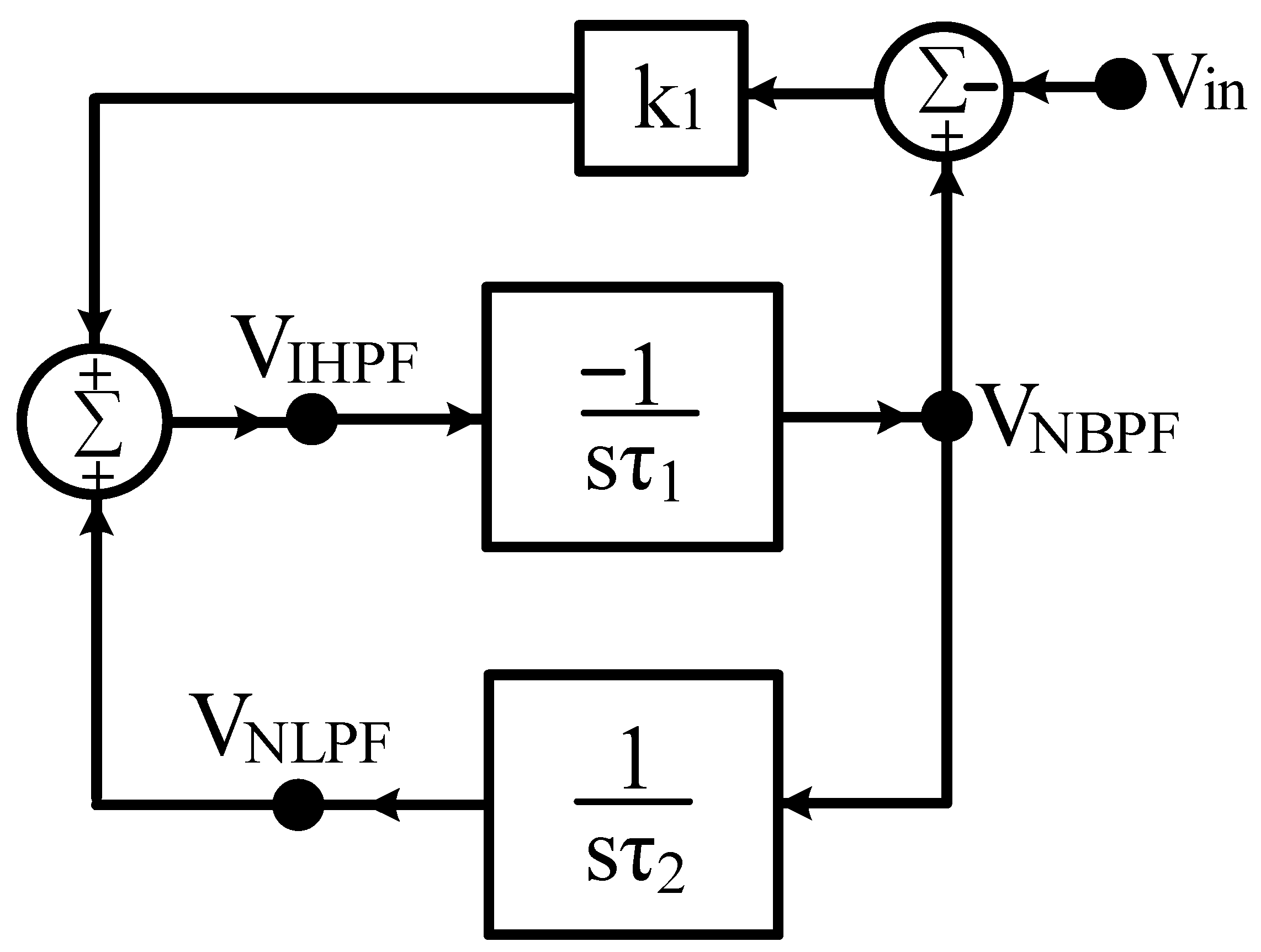
Figure 1.
Synthesis of the first proposed VM LT1228-based filter system module with two integrator loops and a voltage gain building block.
Figure 1.
Synthesis of the first proposed VM LT1228-based filter system module with two integrator loops and a voltage gain building block.
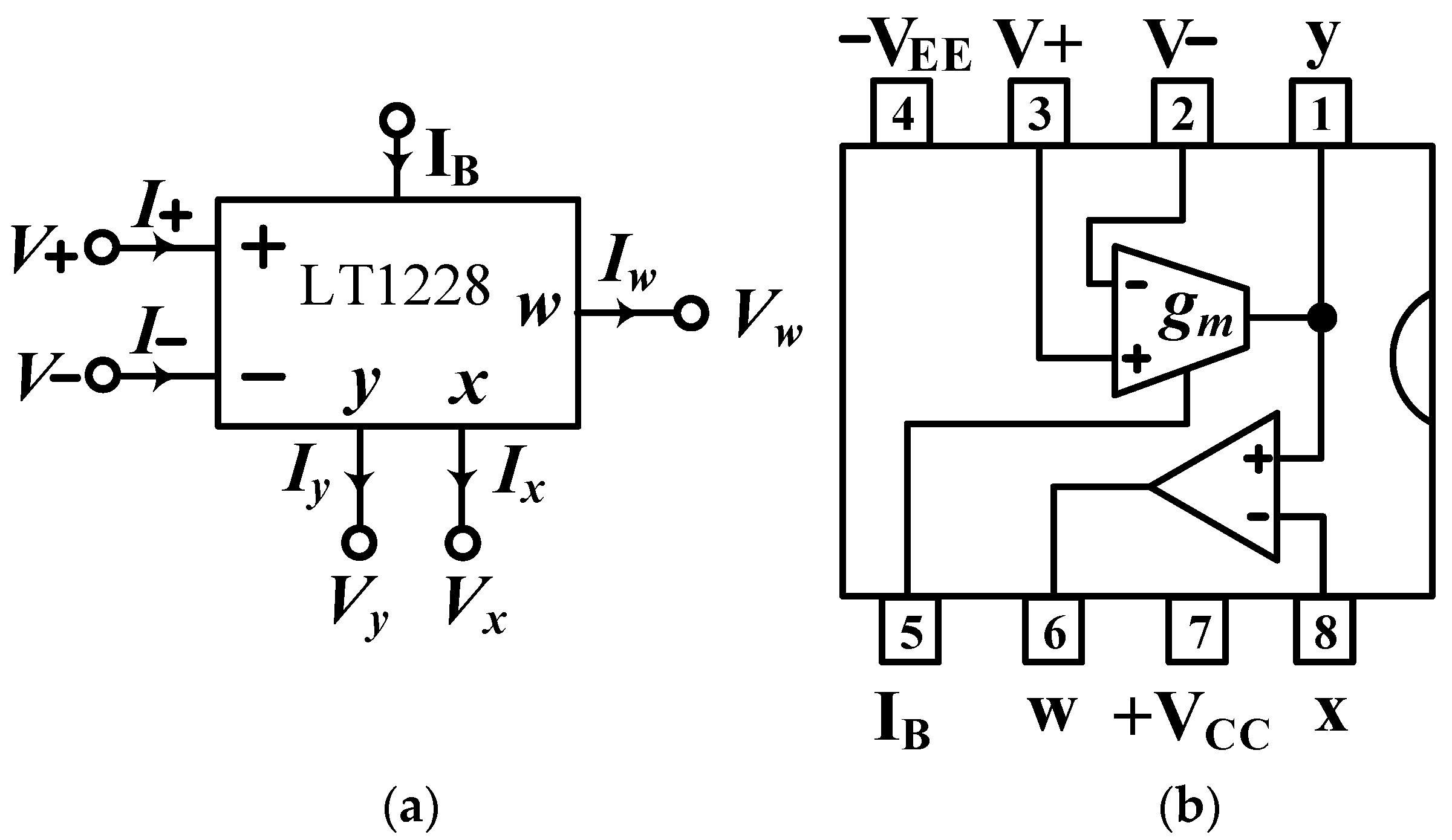
Figure 2.
LT1228 (a) circuit symbol, and (b) IC package in an 8-pin configuration.
Figure 2.
LT1228 (a) circuit symbol, and (b) IC package in an 8-pin configuration.
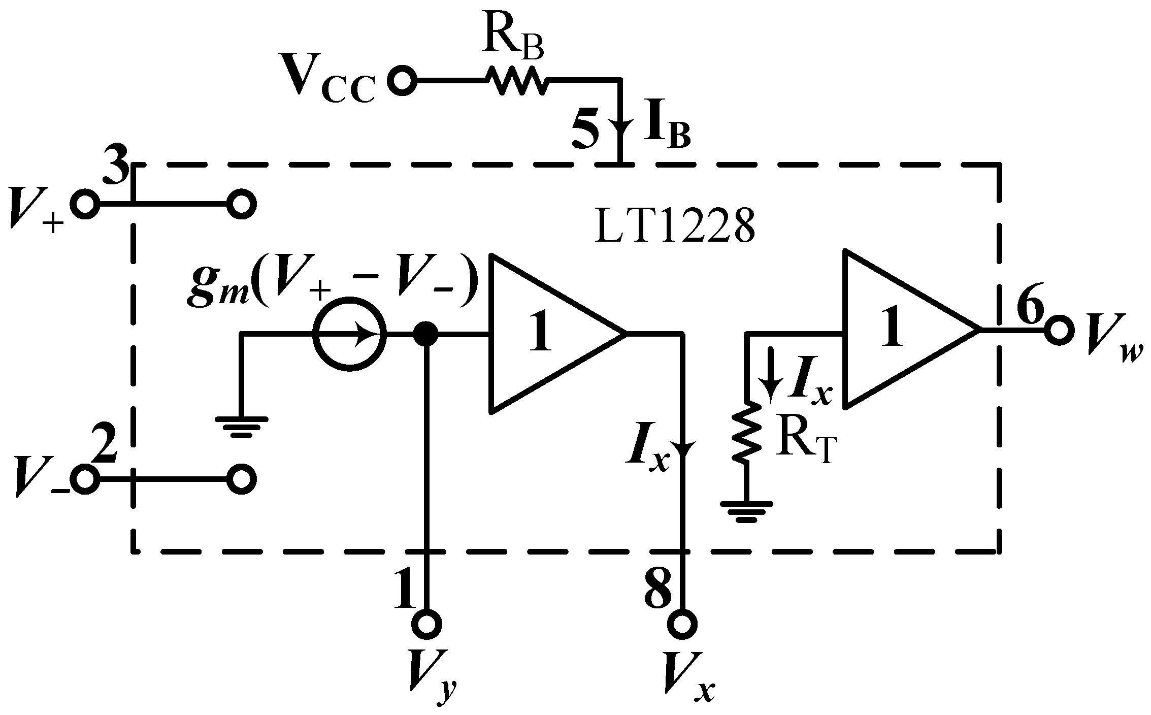
Figure 3.
Equivalent circuit of LT1228.
Figure 3.
Equivalent circuit of LT1228.
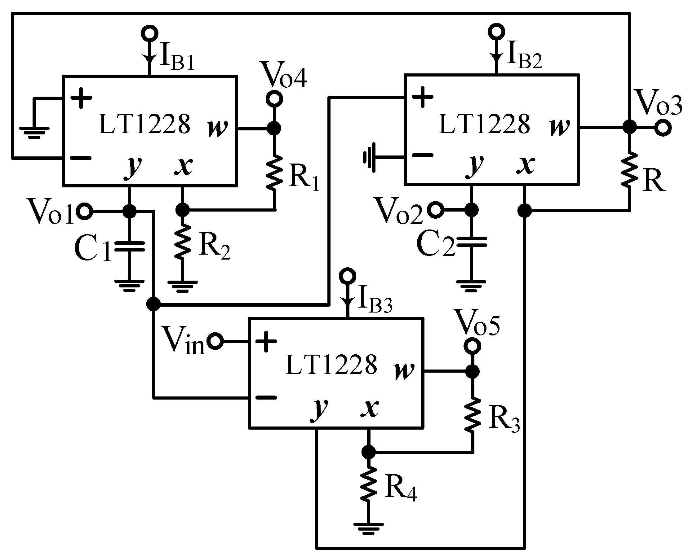
Figure 4.
First proposed VM LT1228-based second-order multifunction filter configuration.
Figure 4.
First proposed VM LT1228-based second-order multifunction filter configuration.
Figure 5.
Synthesis of the second proposed VM LT1228-based filter system module with two integrator loops and a voltage gain building block.
Figure 5.
Synthesis of the second proposed VM LT1228-based filter system module with two integrator loops and a voltage gain building block.
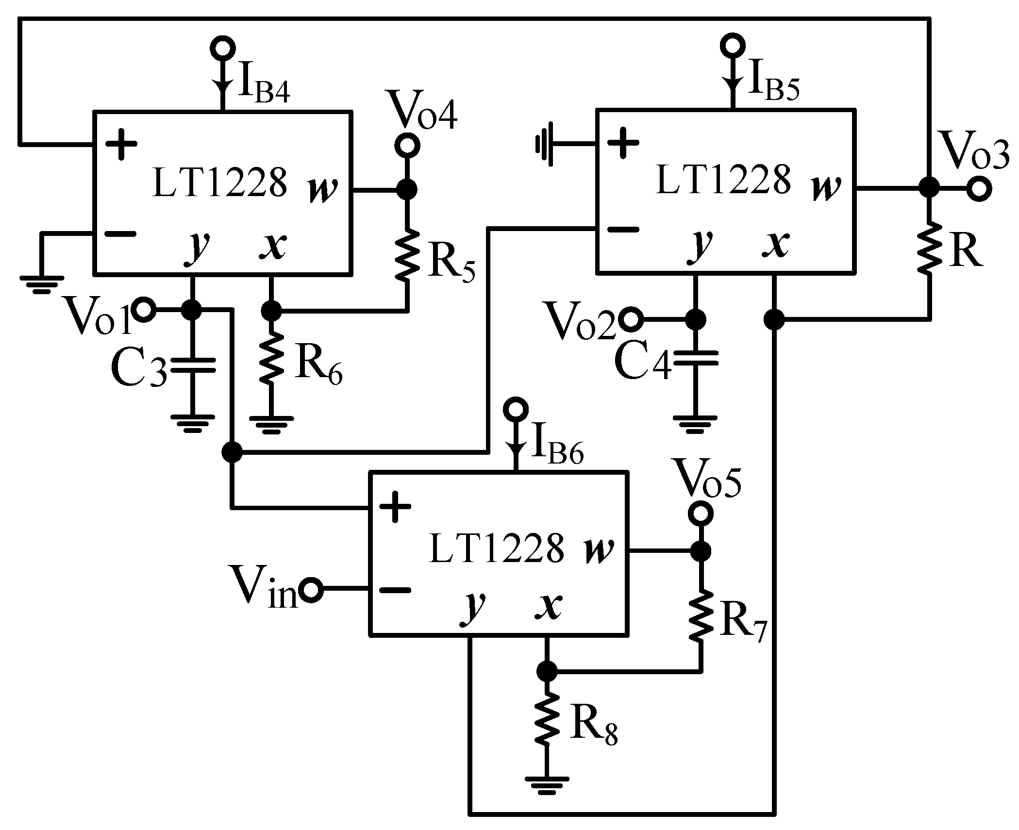
Figure 6.
Second proposed VM LT1228-based second-order multifunction filter configuration.
Figure 6.
Second proposed VM LT1228-based second-order multifunction filter configuration.
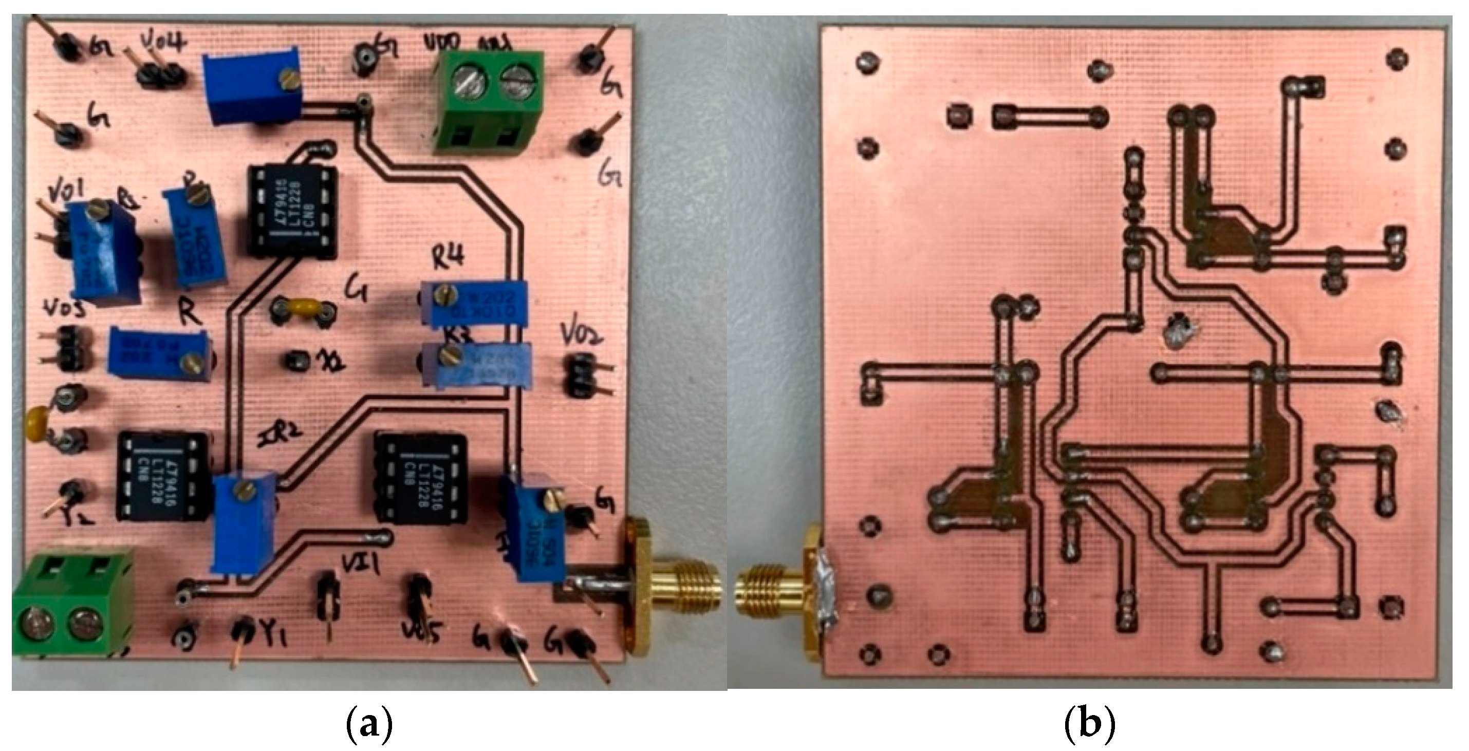
Figure 7.
(
a) Top and (
b) bottom photos of the first proposed VM LT1228-based multifunction filter PCB hardware implementation in
Figure 4.
Figure 7.
(
a) Top and (
b) bottom photos of the first proposed VM LT1228-based multifunction filter PCB hardware implementation in
Figure 4.
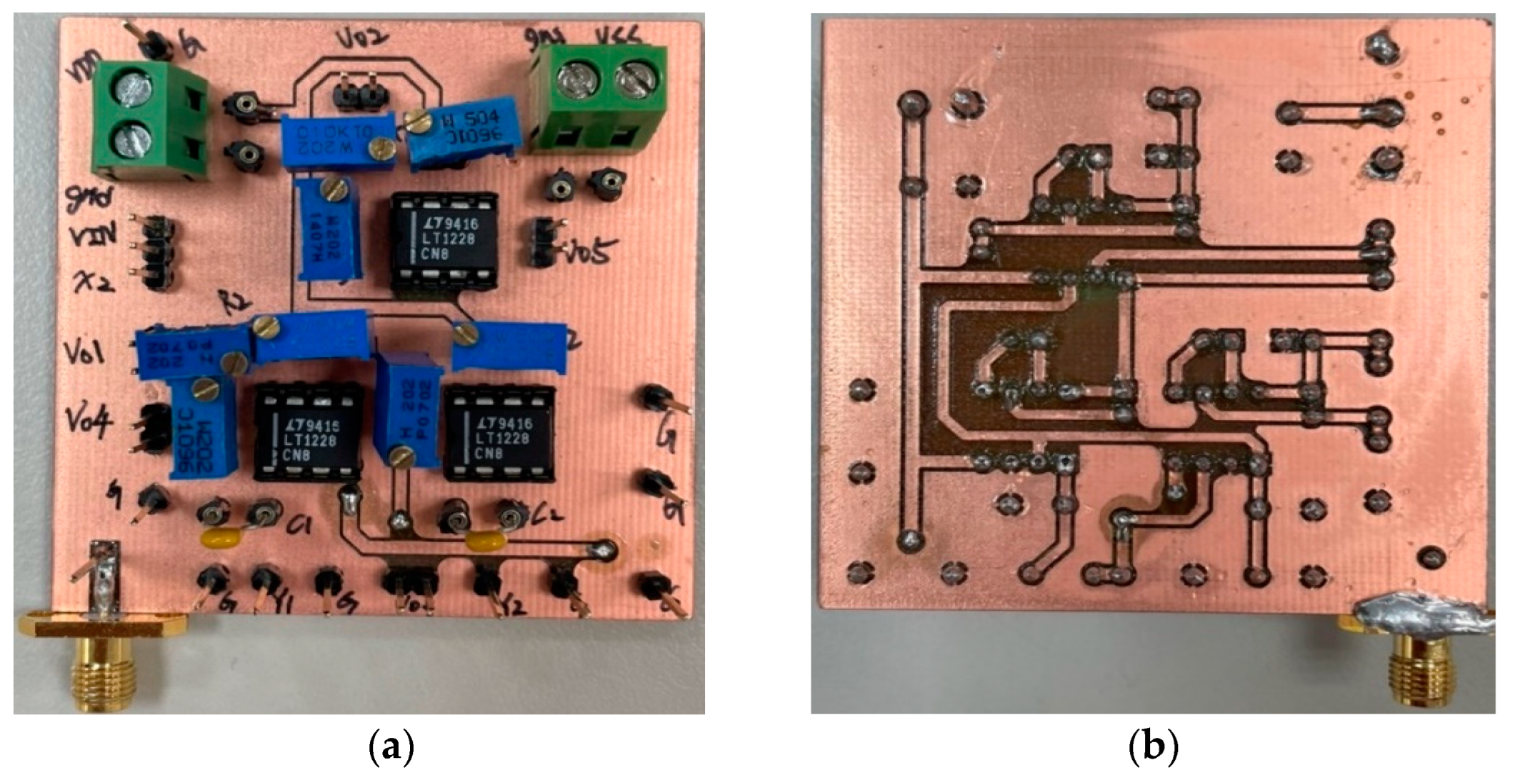
Figure 8.
(
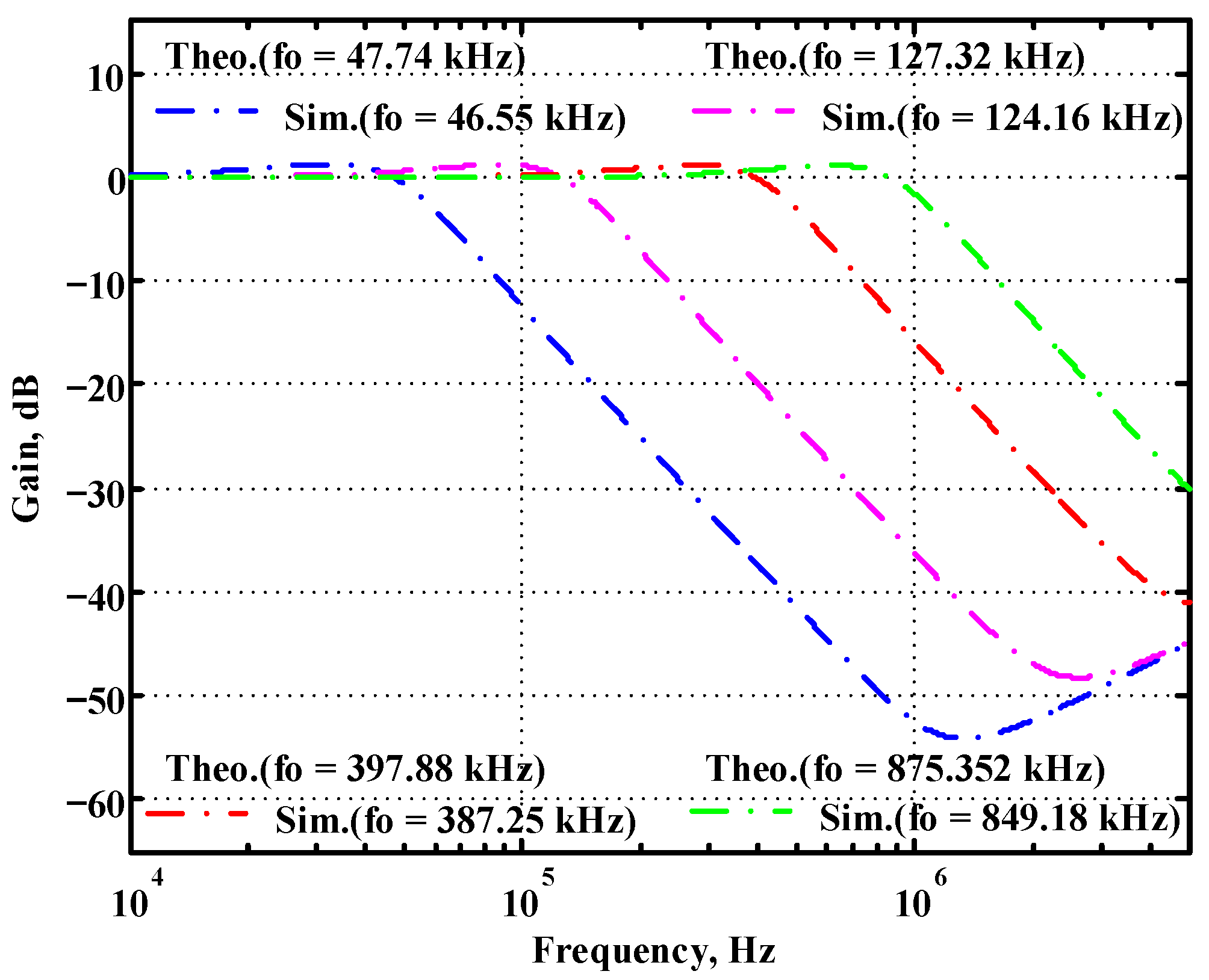
a) Top and (
b) bottom photos of the second proposed VM LT1228-based multifunction filter PCB hardware implementation in
Figure 6.
Figure 8.
(
a) Top and (
b) bottom photos of the second proposed VM LT1228-based multifunction filter PCB hardware implementation in
Figure 6.
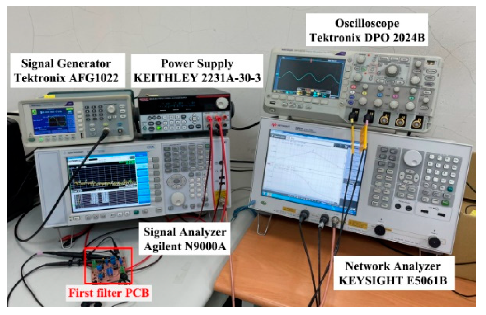
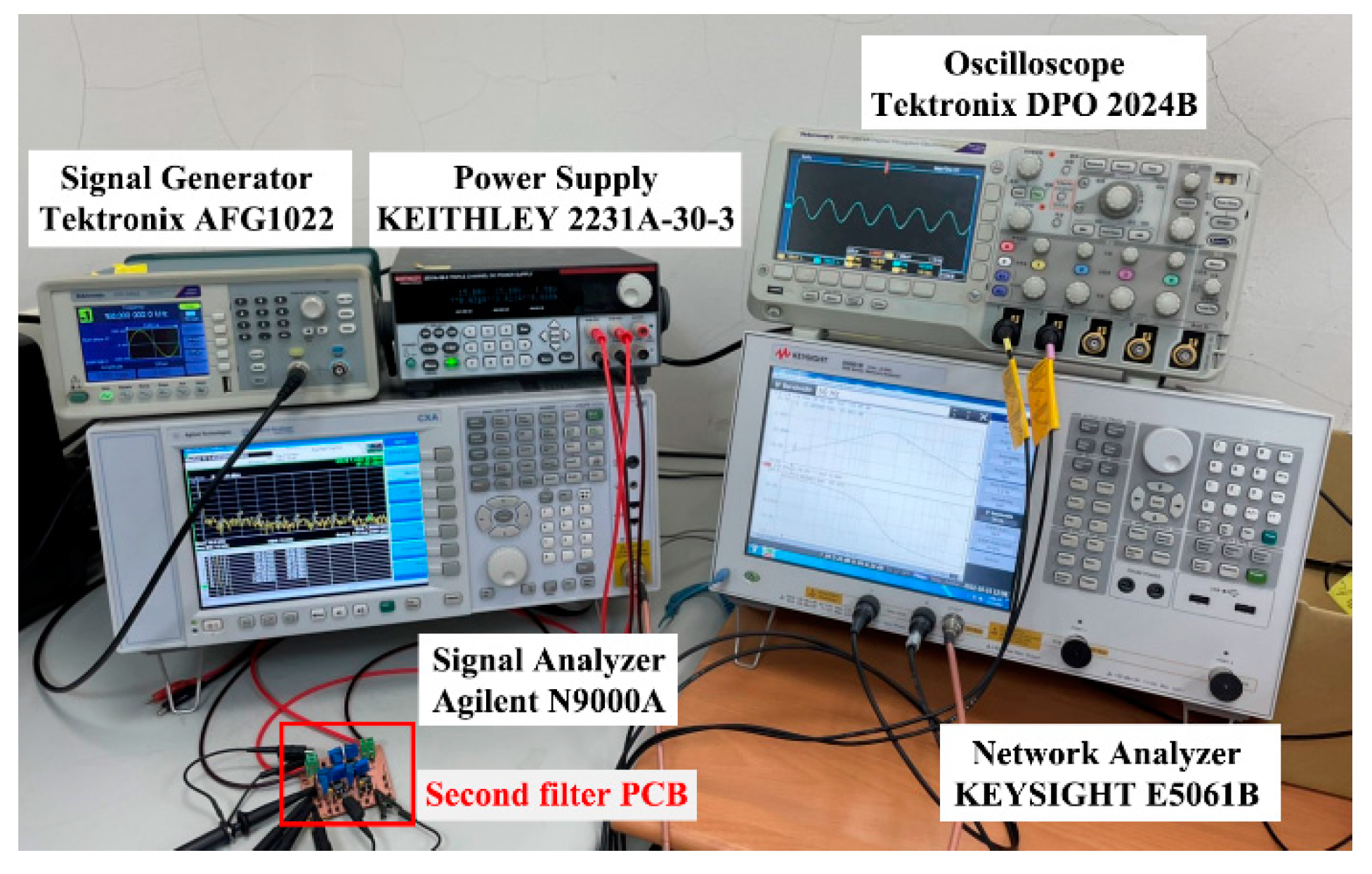
Figure 9.
Experimental hardware setup of the first proposed VM LT1228-based multifunction filter in
Figure 4.
Figure 9.
Experimental hardware setup of the first proposed VM LT1228-based multifunction filter in
Figure 4.
Figure 10.
Experimental hardware setup of the second proposed VM LT1228-based multifunction filter in
Figure 6.
Figure 10.
Experimental hardware setup of the second proposed VM LT1228-based multifunction filter in
Figure 6.
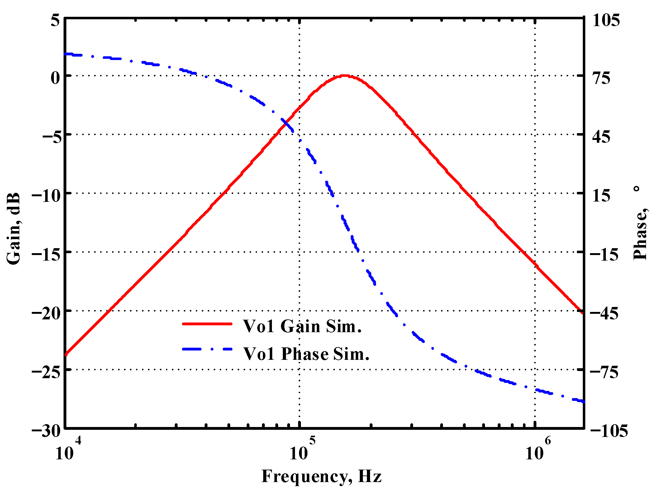
Figure 11.
Simulated gain and phase frequency response of the first proposed circuit at Vo1.
Figure 11.
Simulated gain and phase frequency response of the first proposed circuit at Vo1.
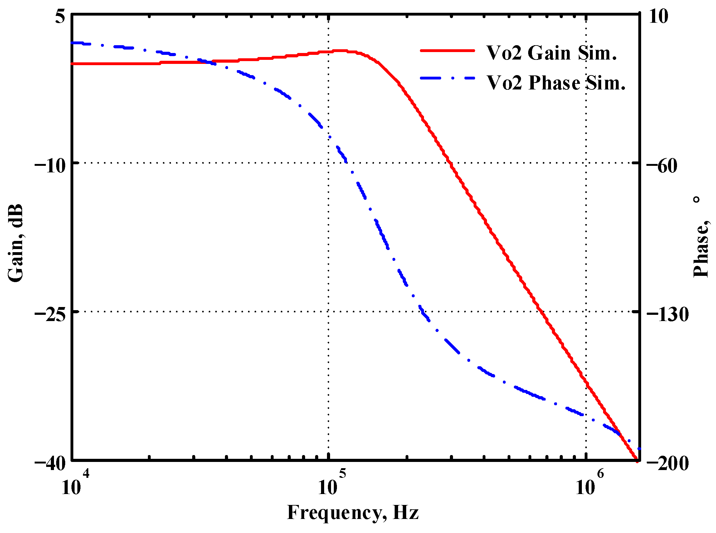
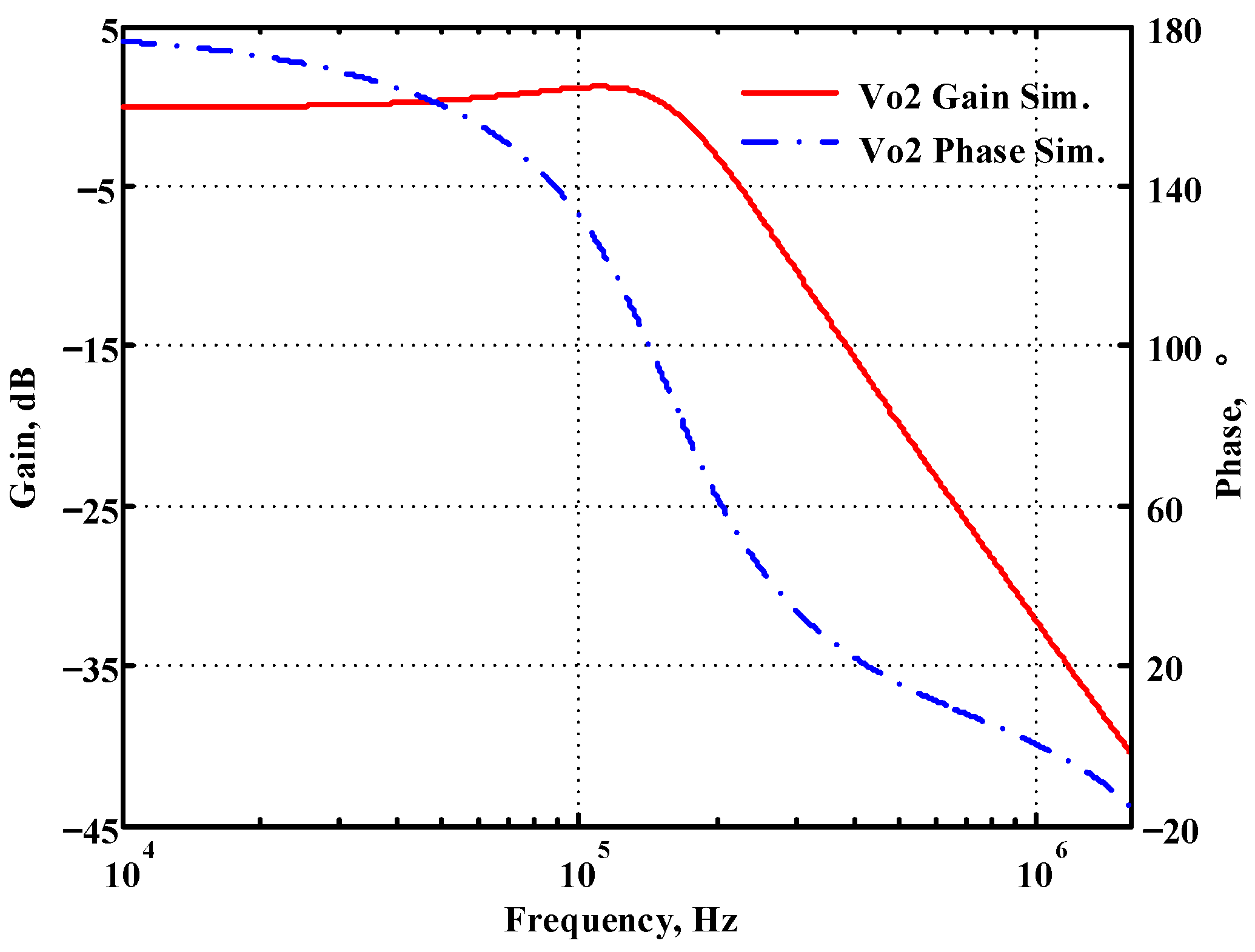
Figure 12.
Simulated gain and phase frequency response of the first proposed circuit at Vo2.
Figure 12.
Simulated gain and phase frequency response of the first proposed circuit at Vo2.
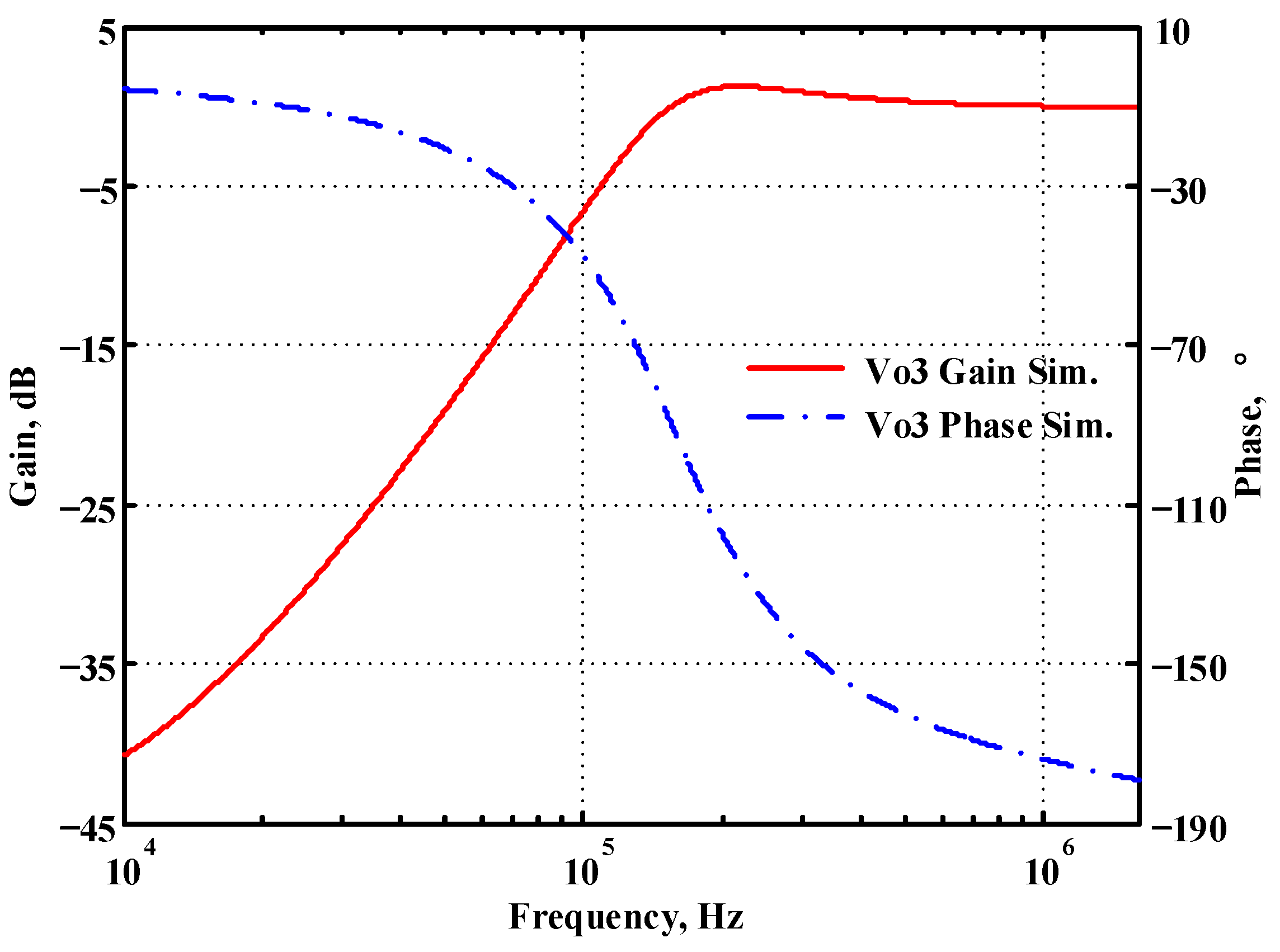
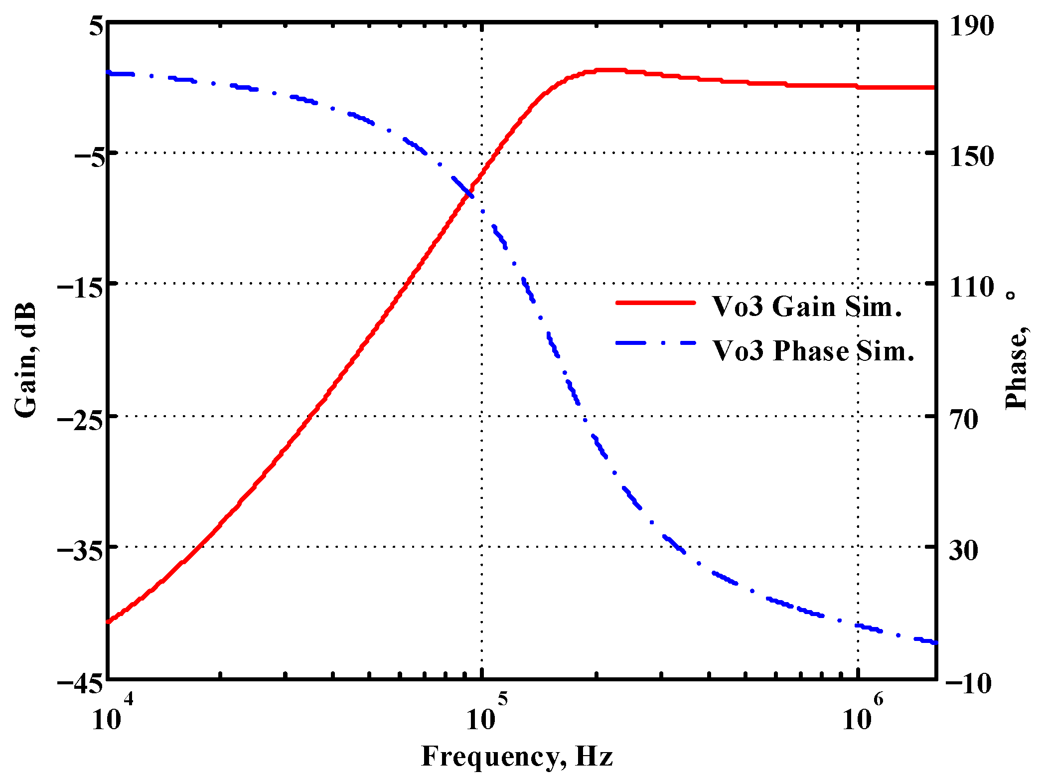
Figure 13.
Simulated gain and phase frequency response of the first proposed circuit at Vo3.
Figure 13.
Simulated gain and phase frequency response of the first proposed circuit at Vo3.
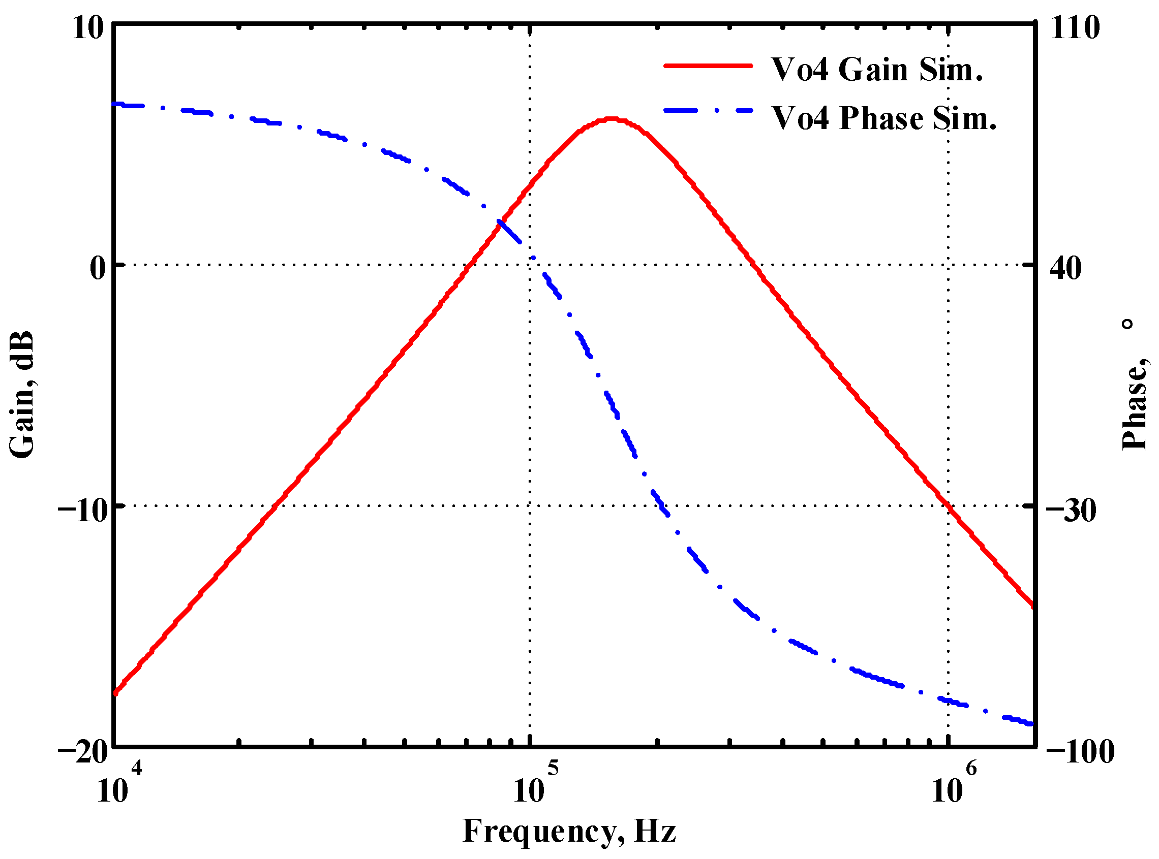
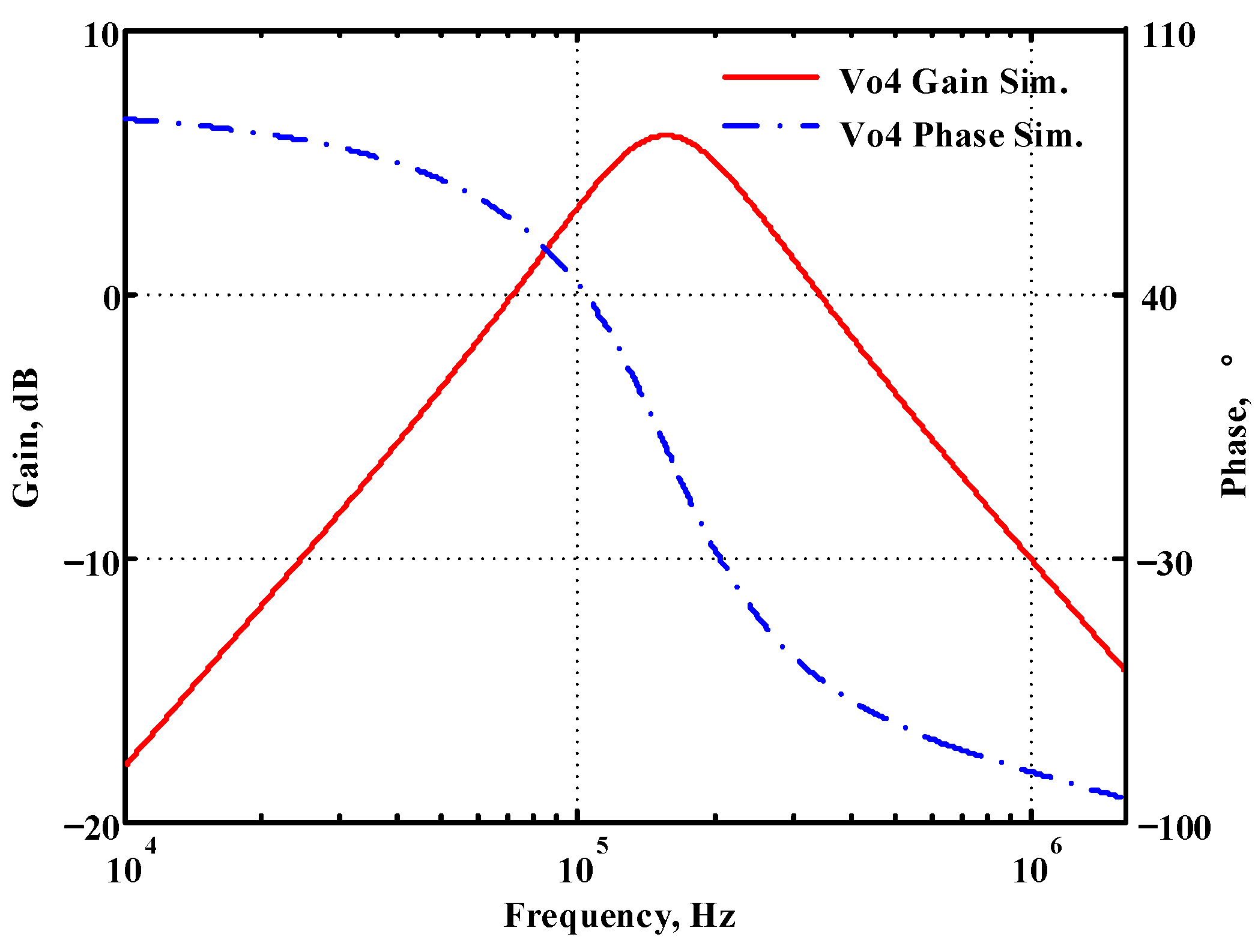
Figure 14.
Simulated gain and phase frequency response of the first proposed circuit at Vo4.
Figure 14.
Simulated gain and phase frequency response of the first proposed circuit at Vo4.
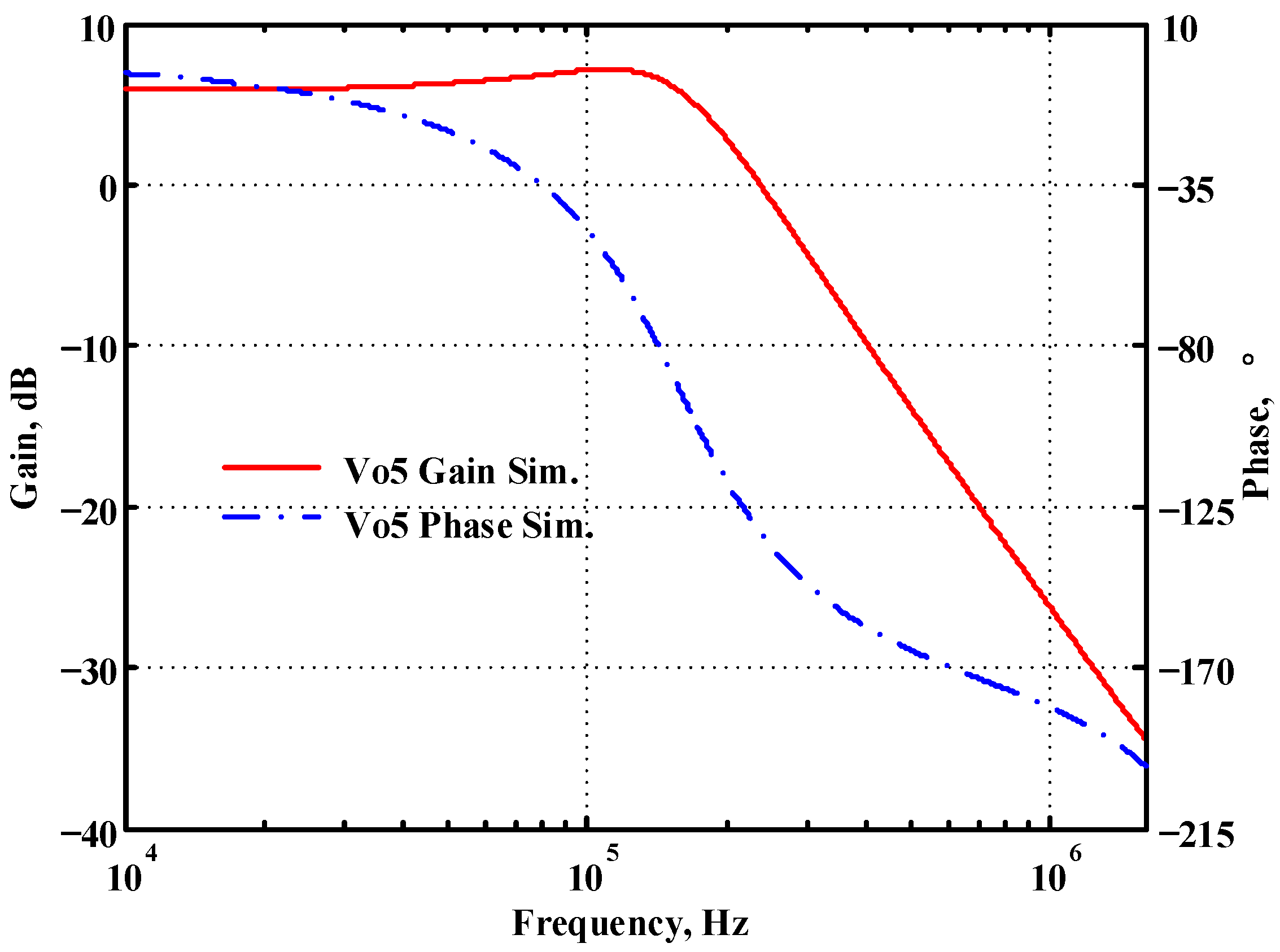
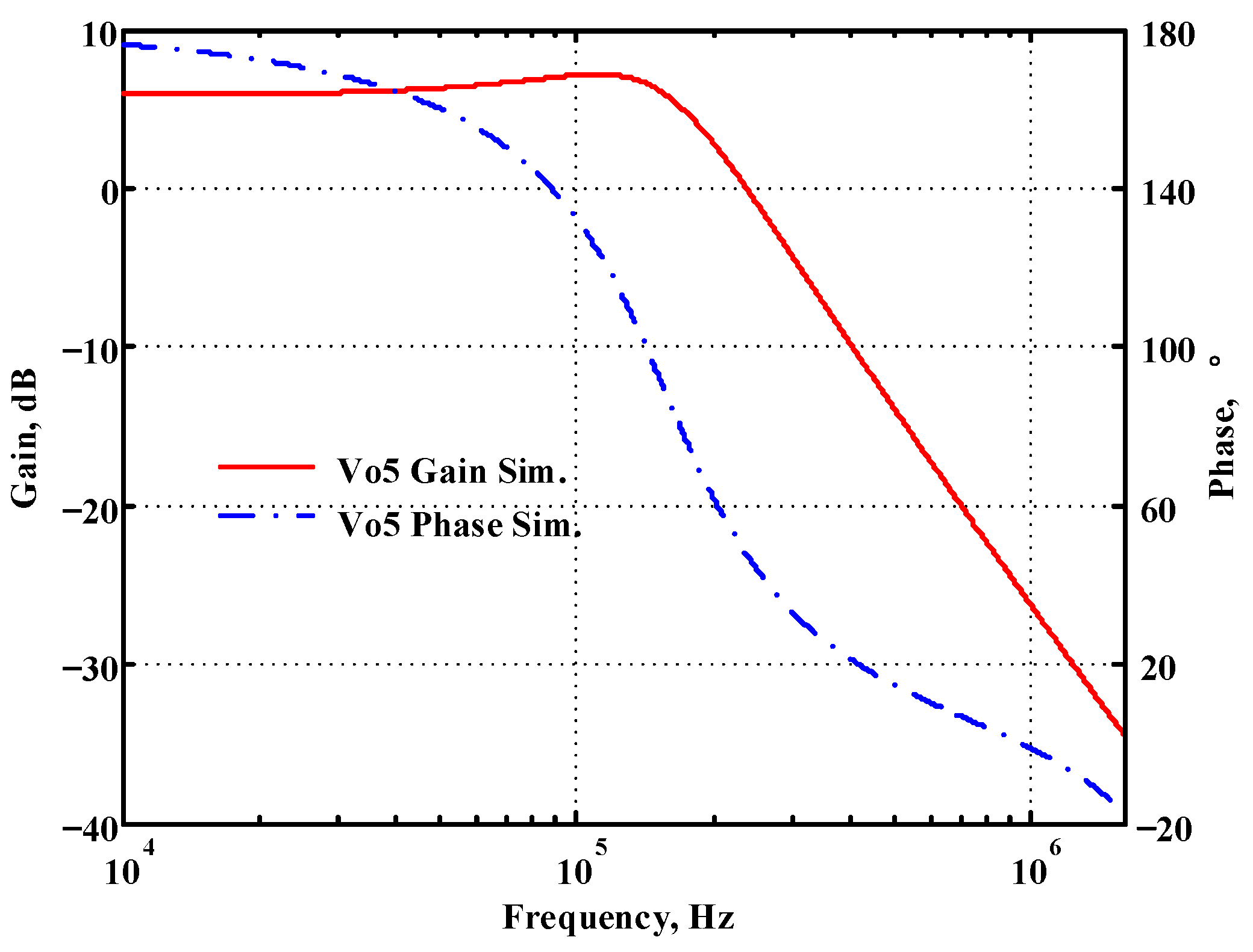
Figure 15.
Simulated gain and phase frequency response of the first proposed circuit at Vo5.
Figure 15.
Simulated gain and phase frequency response of the first proposed circuit at Vo5.
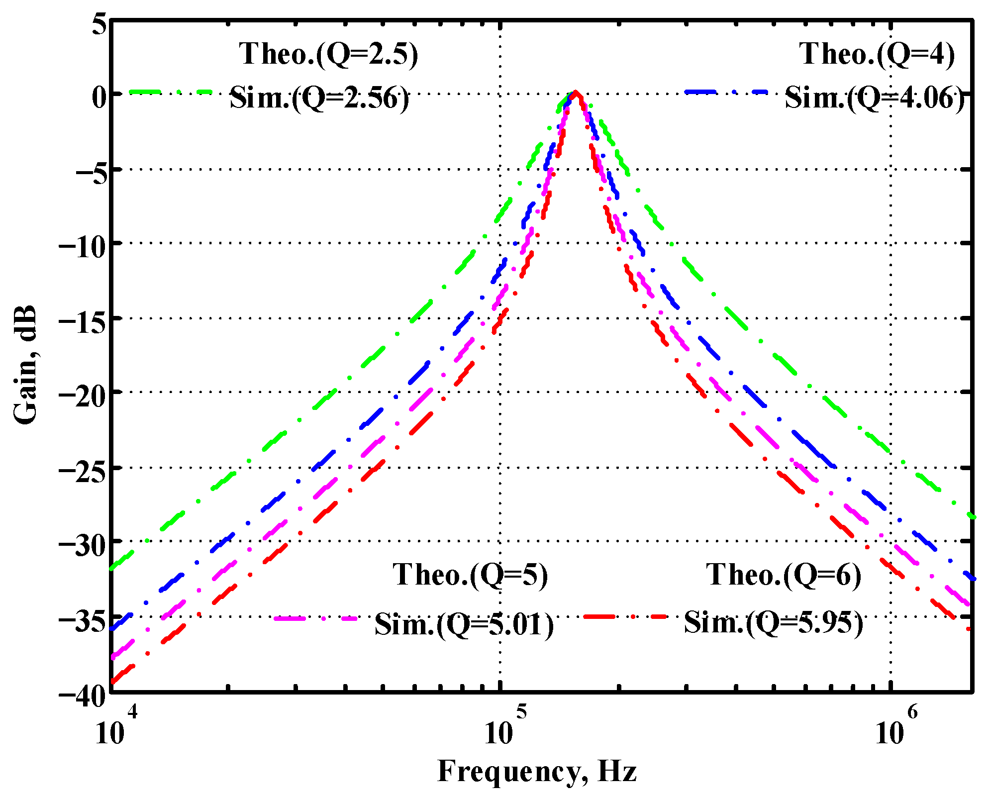
Figure 16.
Simulated gain response of the first proposed circuit at Vo1 by changing Q and keeping fo constant.
Figure 16.
Simulated gain response of the first proposed circuit at Vo1 by changing Q and keeping fo constant.
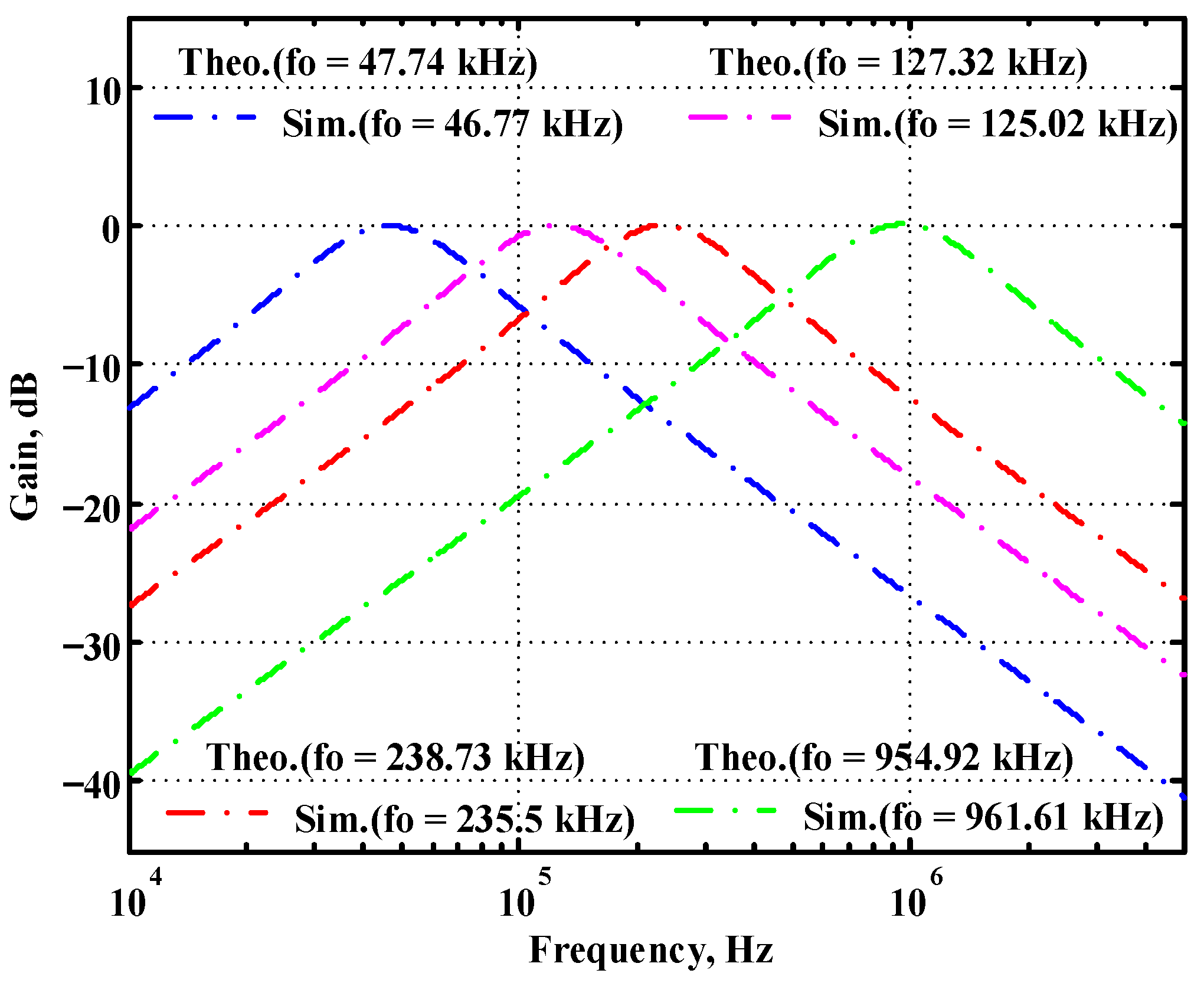
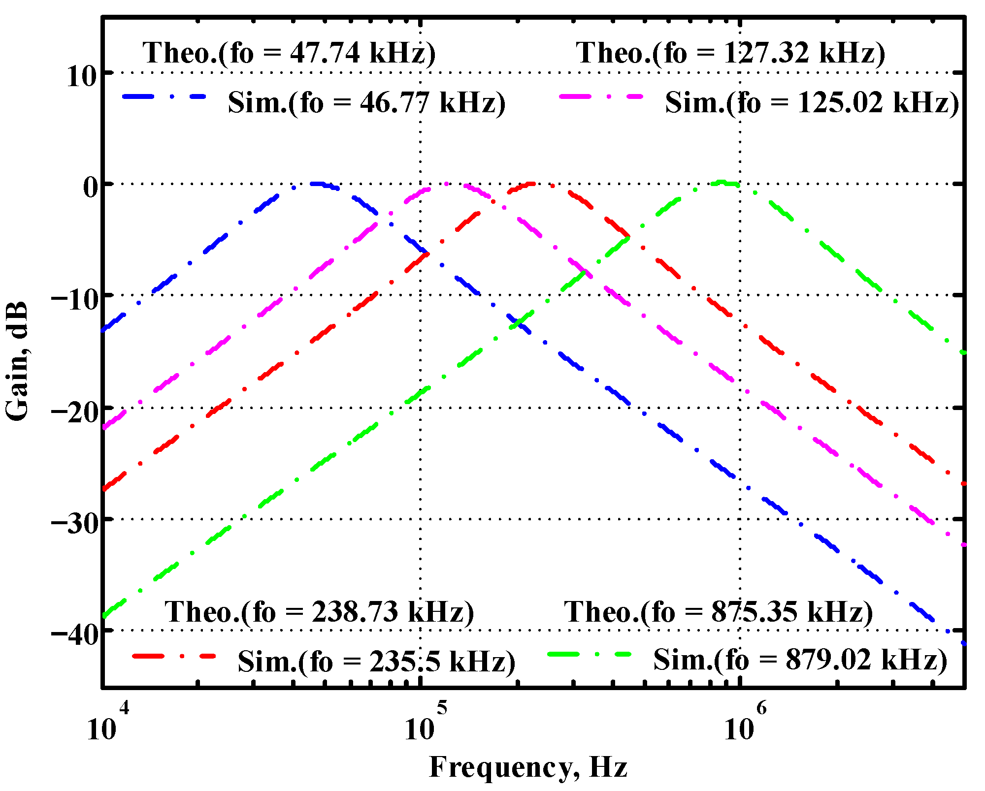
Figure 17.
Simulated gain response of the first proposed circuit at Vo1 by changing fo and keeping Q constant.
Figure 17.
Simulated gain response of the first proposed circuit at Vo1 by changing fo and keeping Q constant.
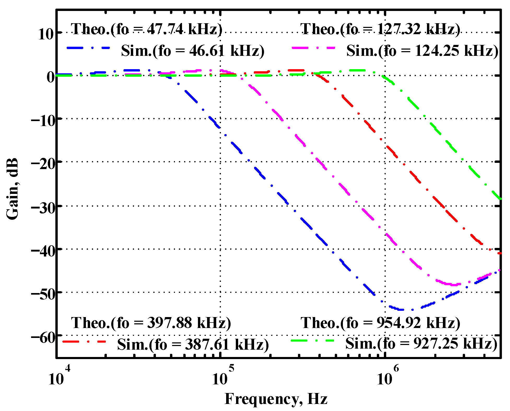
Figure 18.
Simulated gain response of the first proposed circuit at Vo2 by changing fo and keeping Q constant.
Figure 18.
Simulated gain response of the first proposed circuit at Vo2 by changing fo and keeping Q constant.
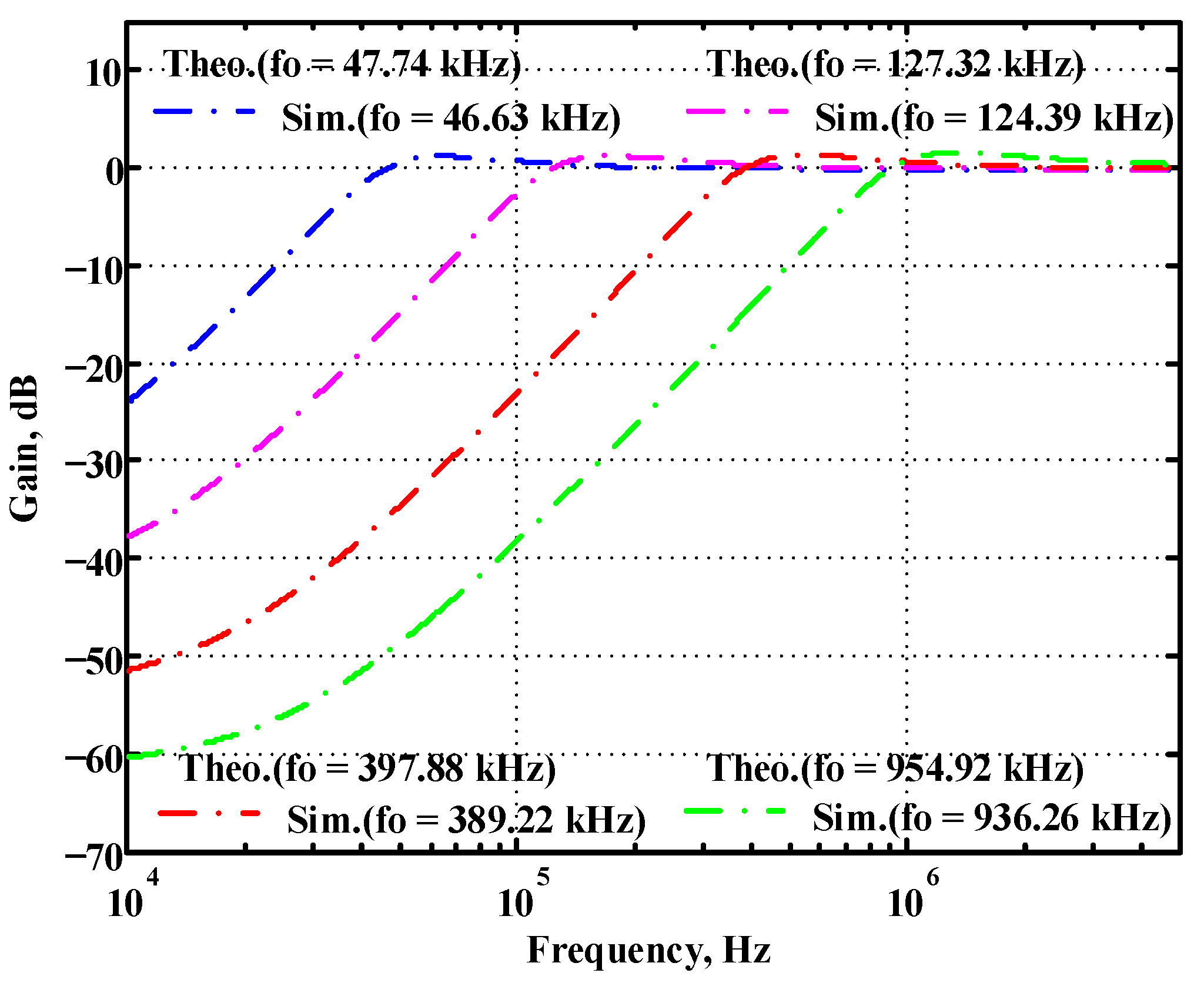
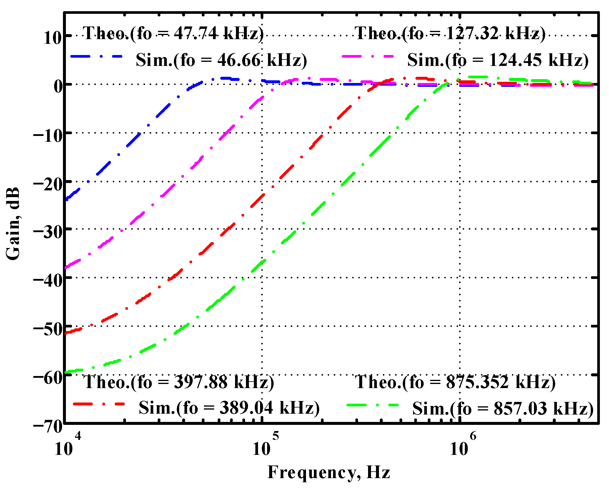
Figure 19.
Simulated gain response of the first proposed circuit at Vo3 by changing fo and keeping Q constant.
Figure 19.
Simulated gain response of the first proposed circuit at Vo3 by changing fo and keeping Q constant.
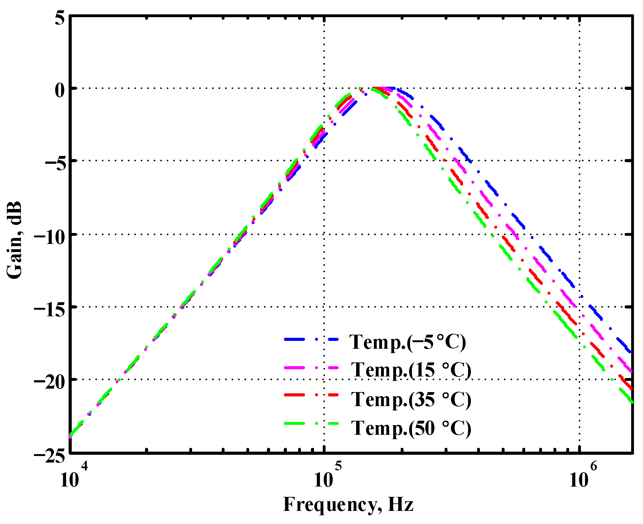
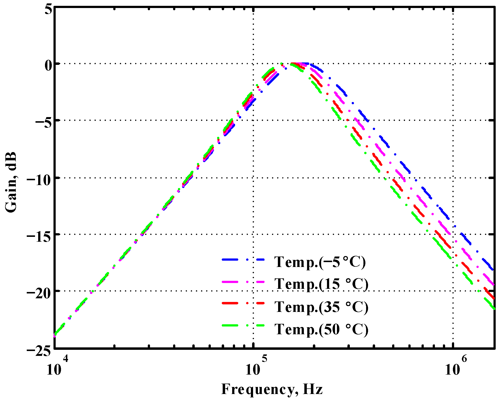
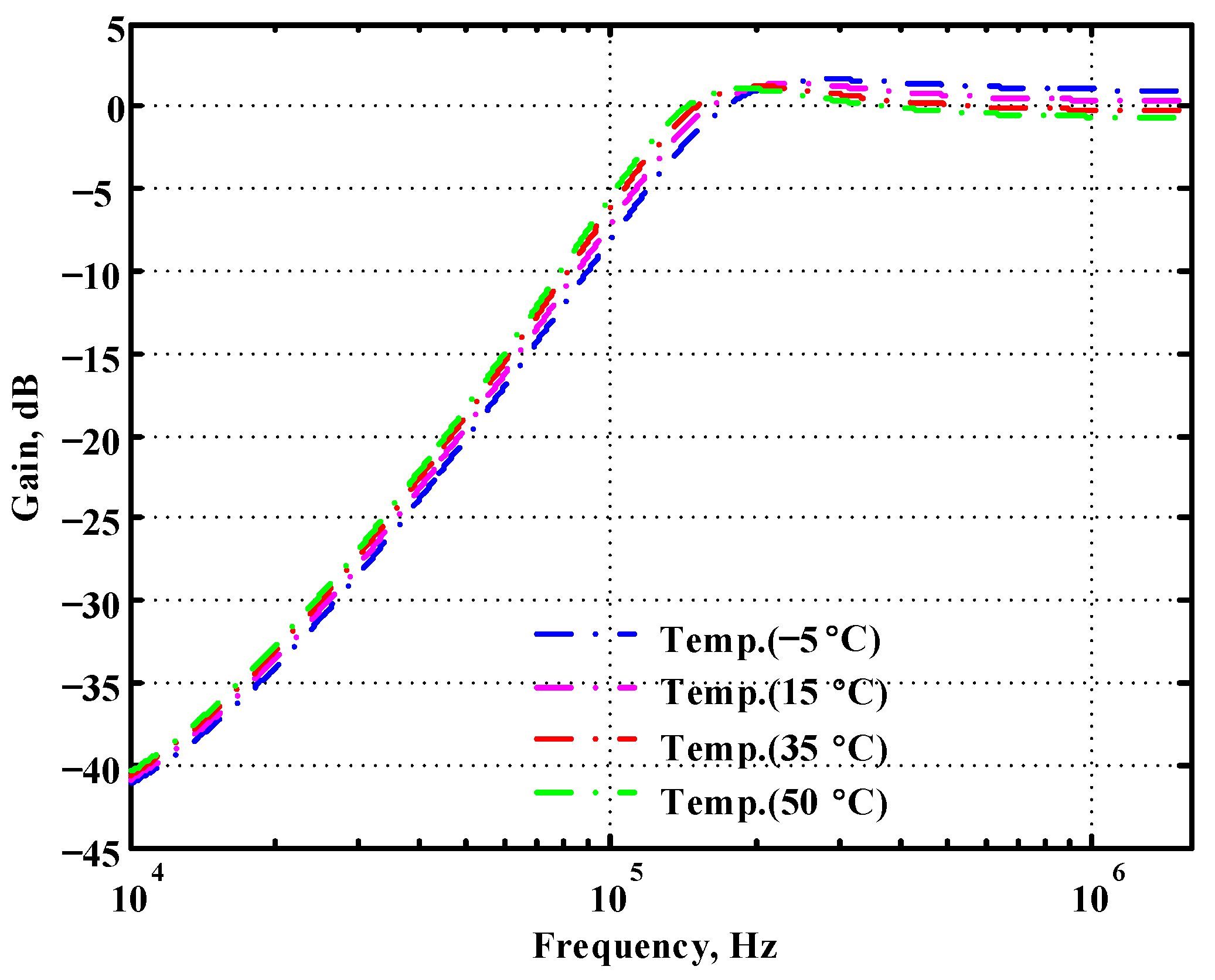
Figure 20.
Simulated temperature variation at Vo1 for the first proposed circuit.
Figure 20.
Simulated temperature variation at Vo1 for the first proposed circuit.
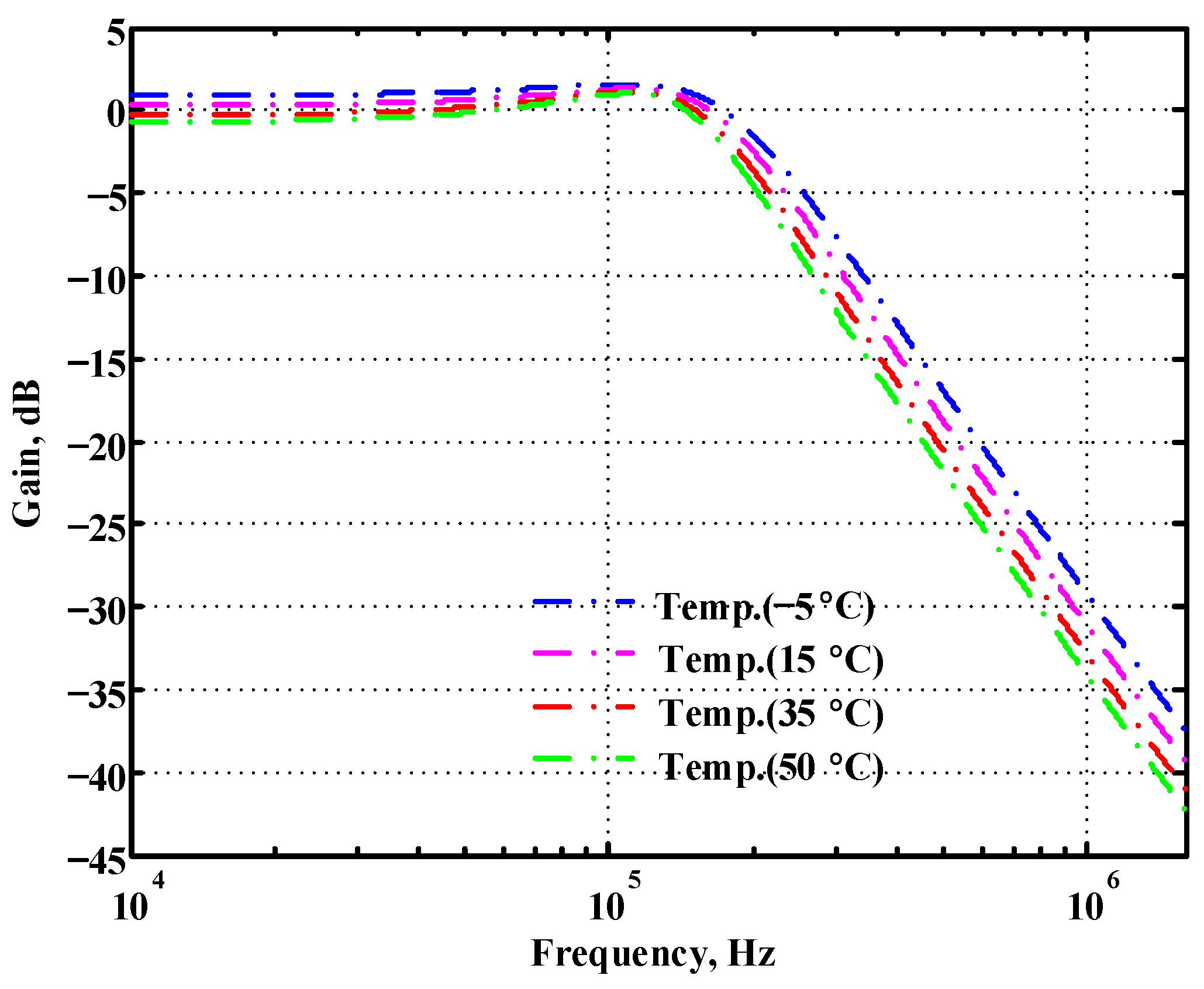
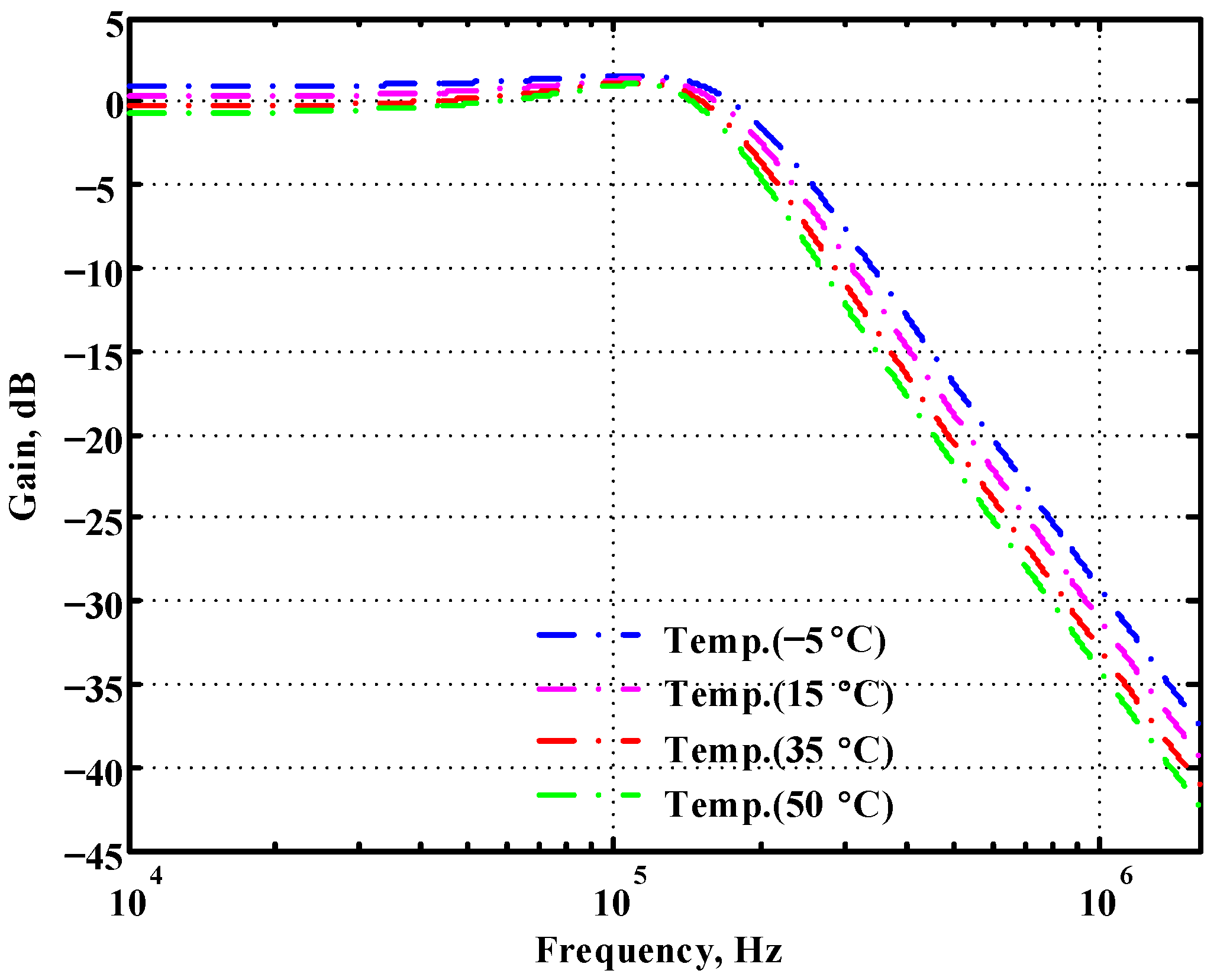
Figure 21.
Simulated temperature variation at Vo2 for the first proposed circuit.
Figure 21.
Simulated temperature variation at Vo2 for the first proposed circuit.
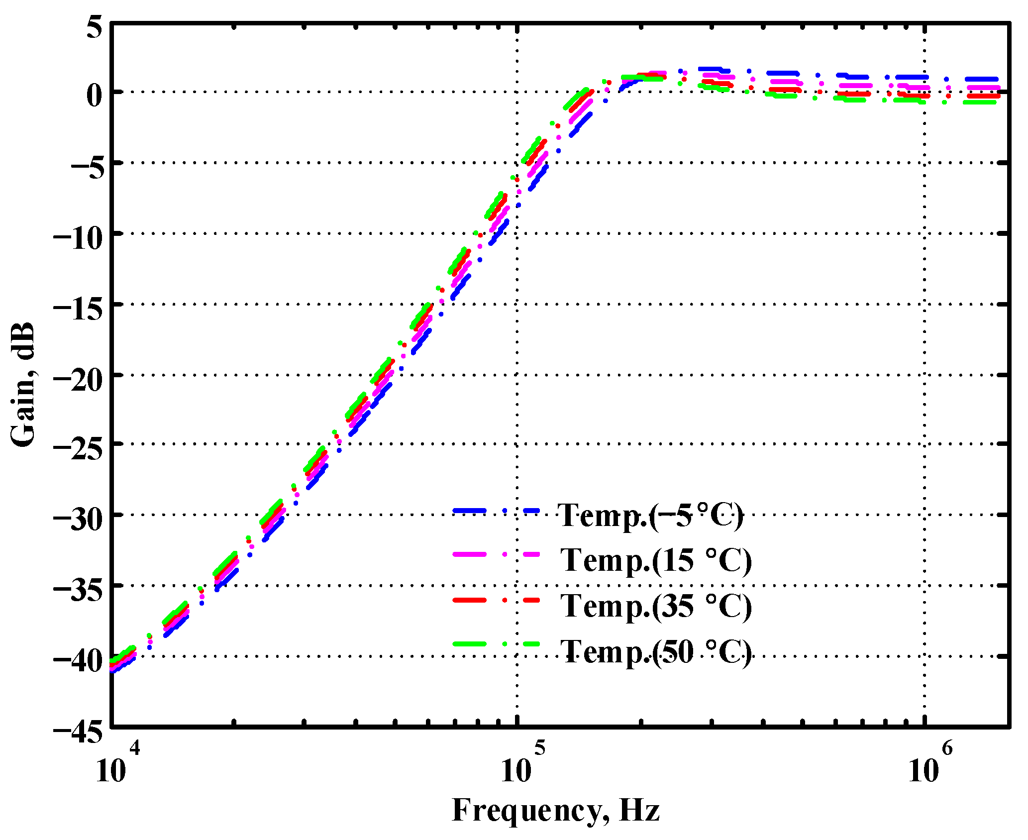
Figure 22.
Simulated temperature variation at Vo3 for the first proposed circuit.
Figure 22.
Simulated temperature variation at Vo3 for the first proposed circuit.
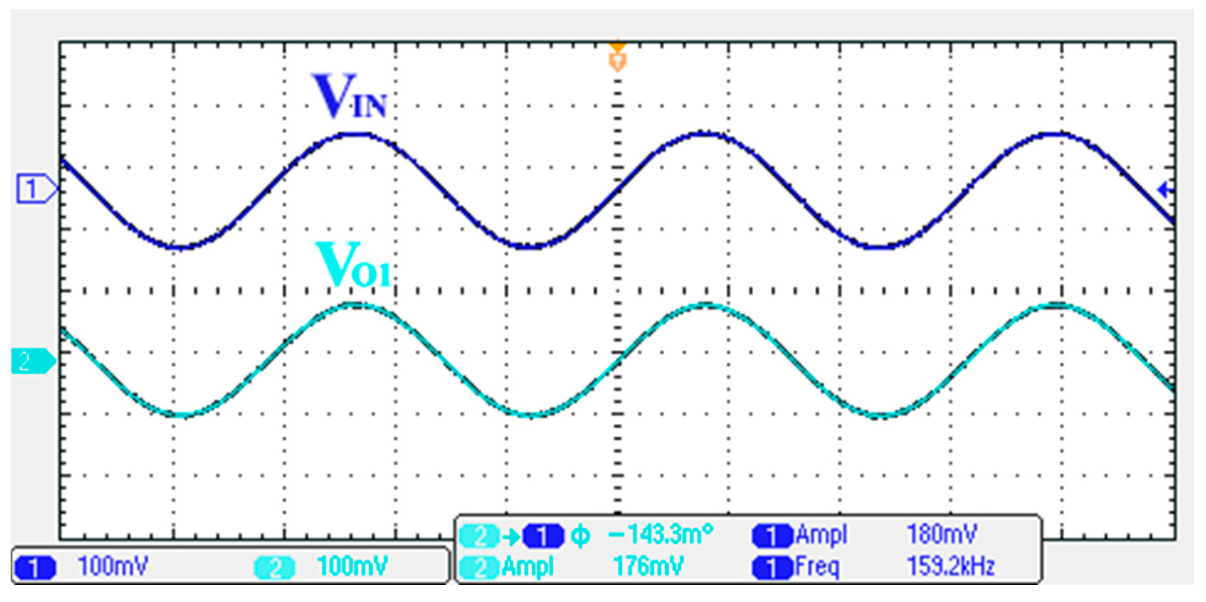
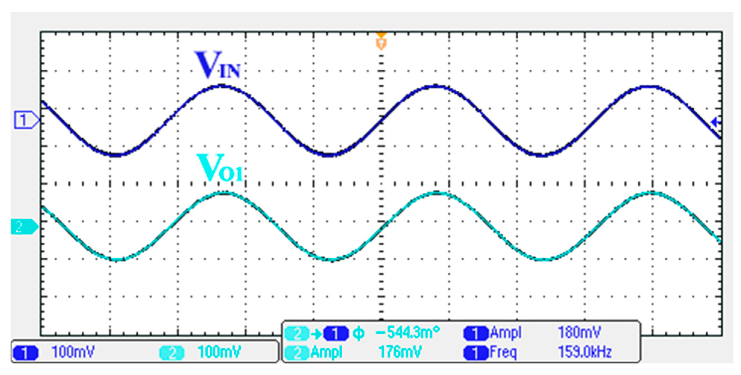
Figure 23.
Measured output and input characteristics of the first proposed circuit at Vo1.
Figure 23.
Measured output and input characteristics of the first proposed circuit at Vo1.
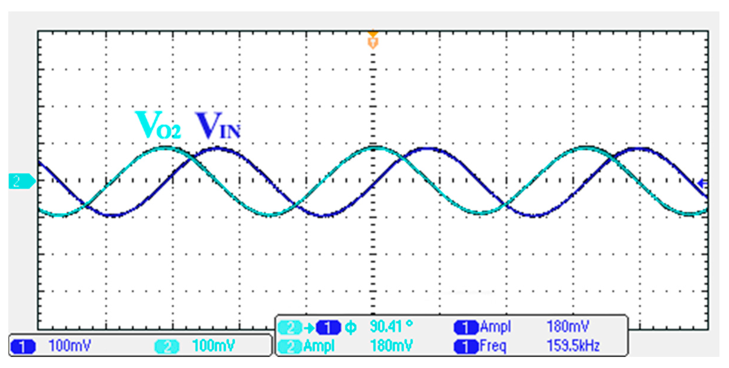
Figure 24.
Measured output and input characteristics of the first proposed circuit at Vo2.
Figure 24.
Measured output and input characteristics of the first proposed circuit at Vo2.
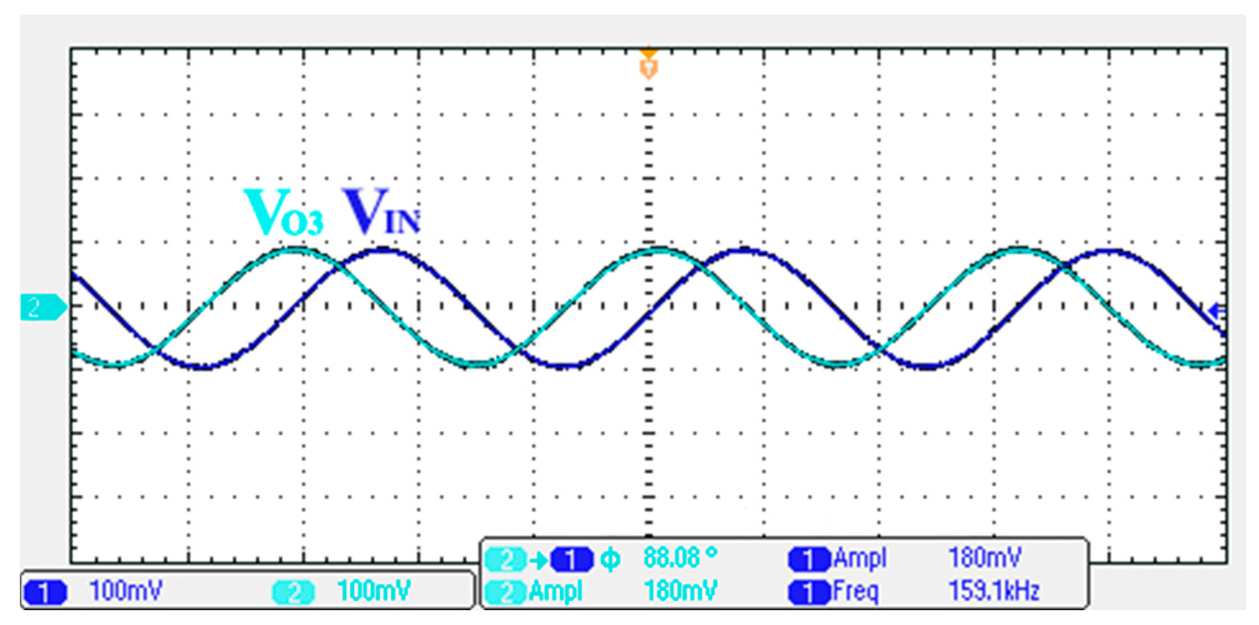
Figure 25.
Measured output and input characteristics of the first proposed circuit at Vo3.
Figure 25.
Measured output and input characteristics of the first proposed circuit at Vo3.
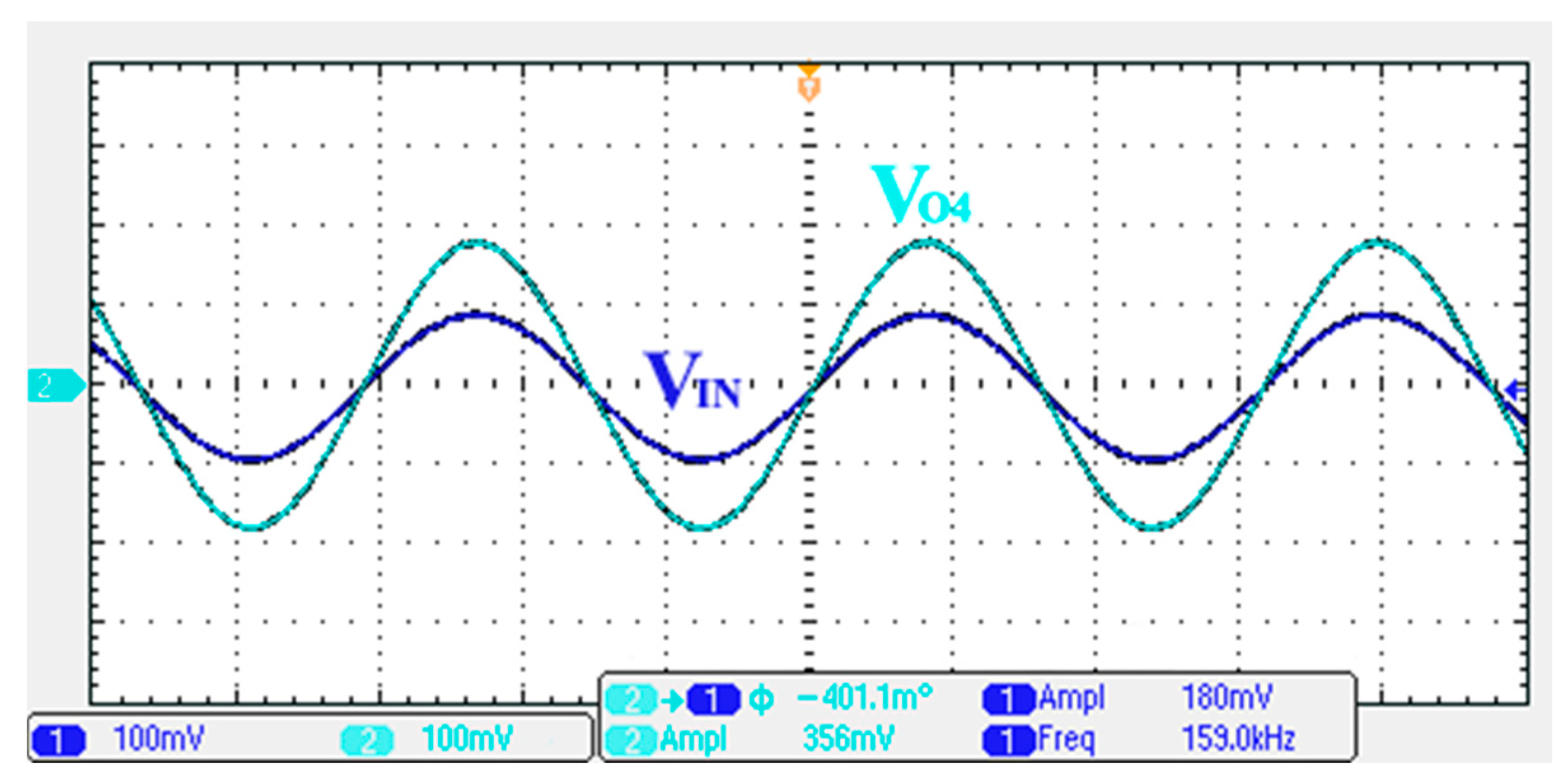
Figure 26.
Measured output and input characteristics of the first proposed circuit at Vo4.
Figure 26.
Measured output and input characteristics of the first proposed circuit at Vo4.
Figure 27.
Measured output and input characteristics of the first proposed circuit at Vo5.
Figure 27.
Measured output and input characteristics of the first proposed circuit at Vo5.
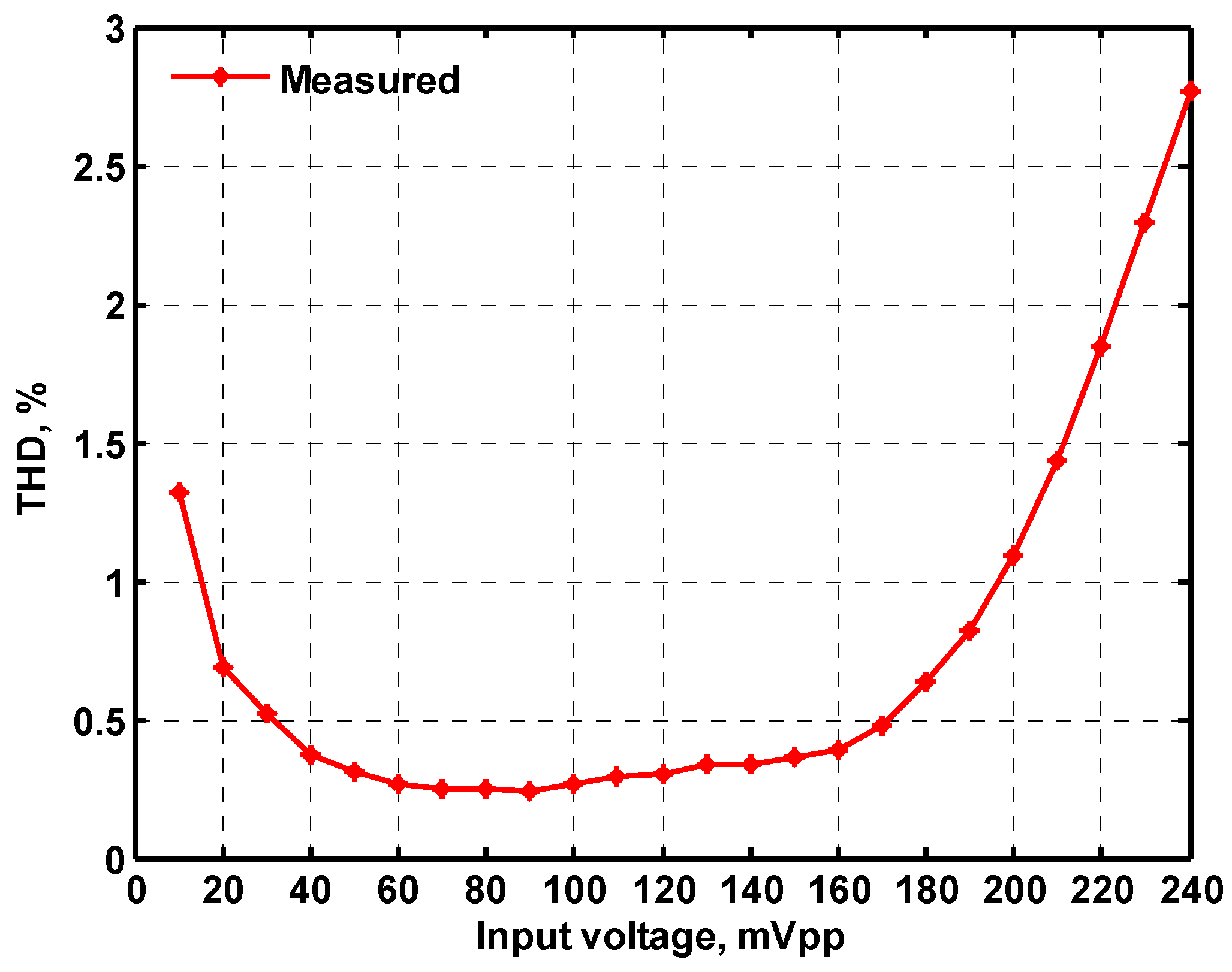
Figure 28.
Measured THD of the first proposed circuit at V
o1 in
Figure 4 versus peak-to-peak input voltage signal at 159.15 kHz.
Figure 28.
Measured THD of the first proposed circuit at V
o1 in
Figure 4 versus peak-to-peak input voltage signal at 159.15 kHz.
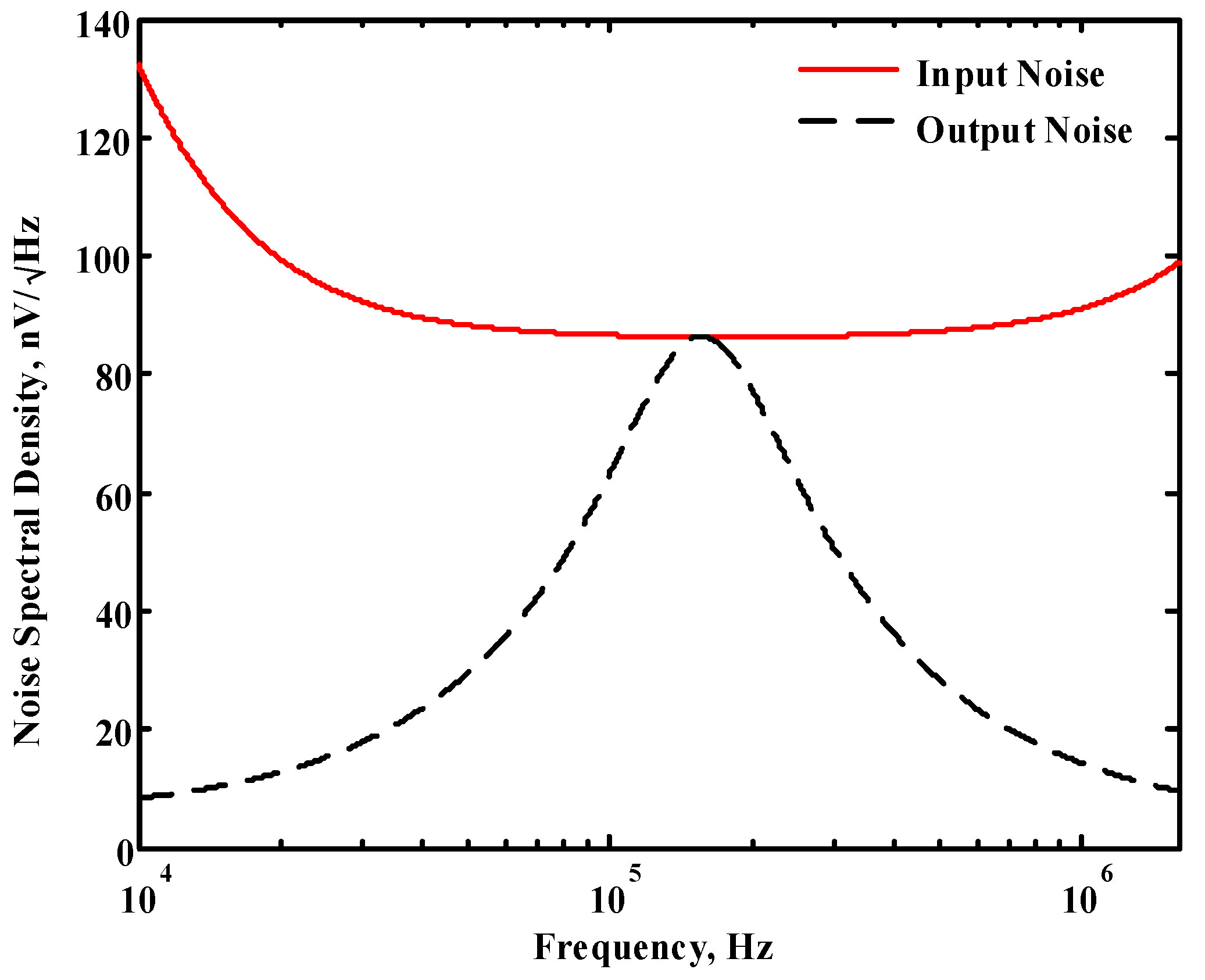
Figure 29.
Simulated noise performance of the first proposed circuit at Vo1.
Figure 29.
Simulated noise performance of the first proposed circuit at Vo1.
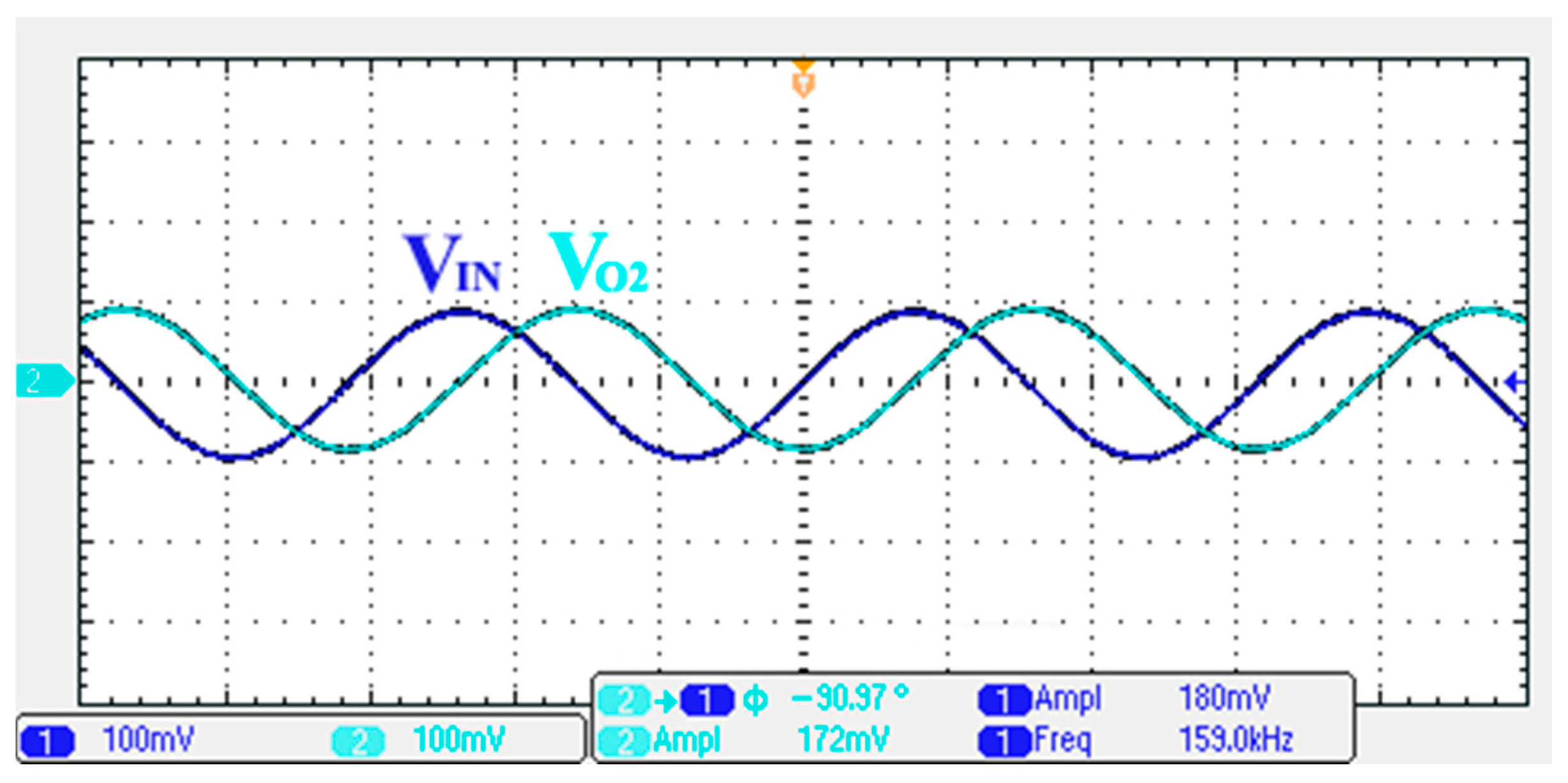
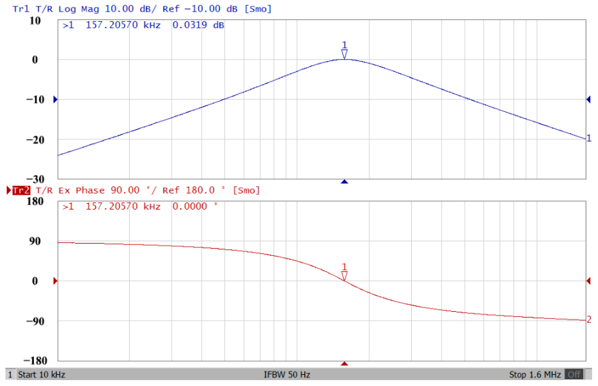
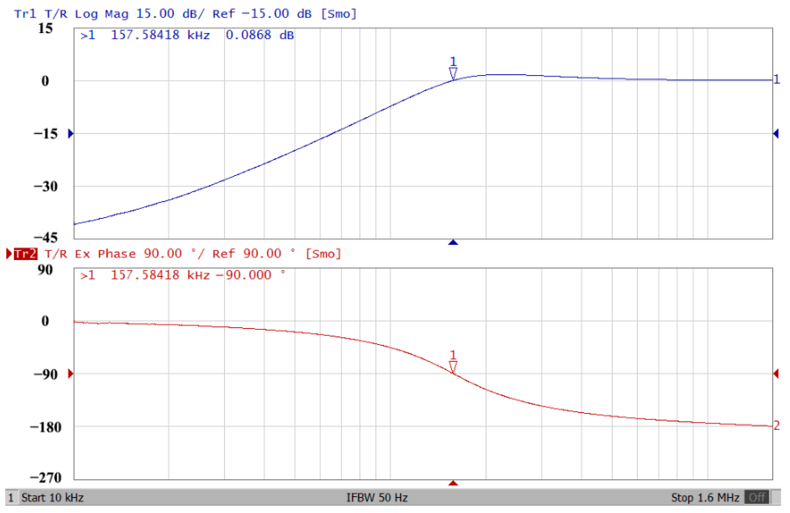
Figure 30.
Frequency-domain characteristics of the measured amplitude and phase responses of the first proposed circuit at Vo1.
Figure 30.
Frequency-domain characteristics of the measured amplitude and phase responses of the first proposed circuit at Vo1.
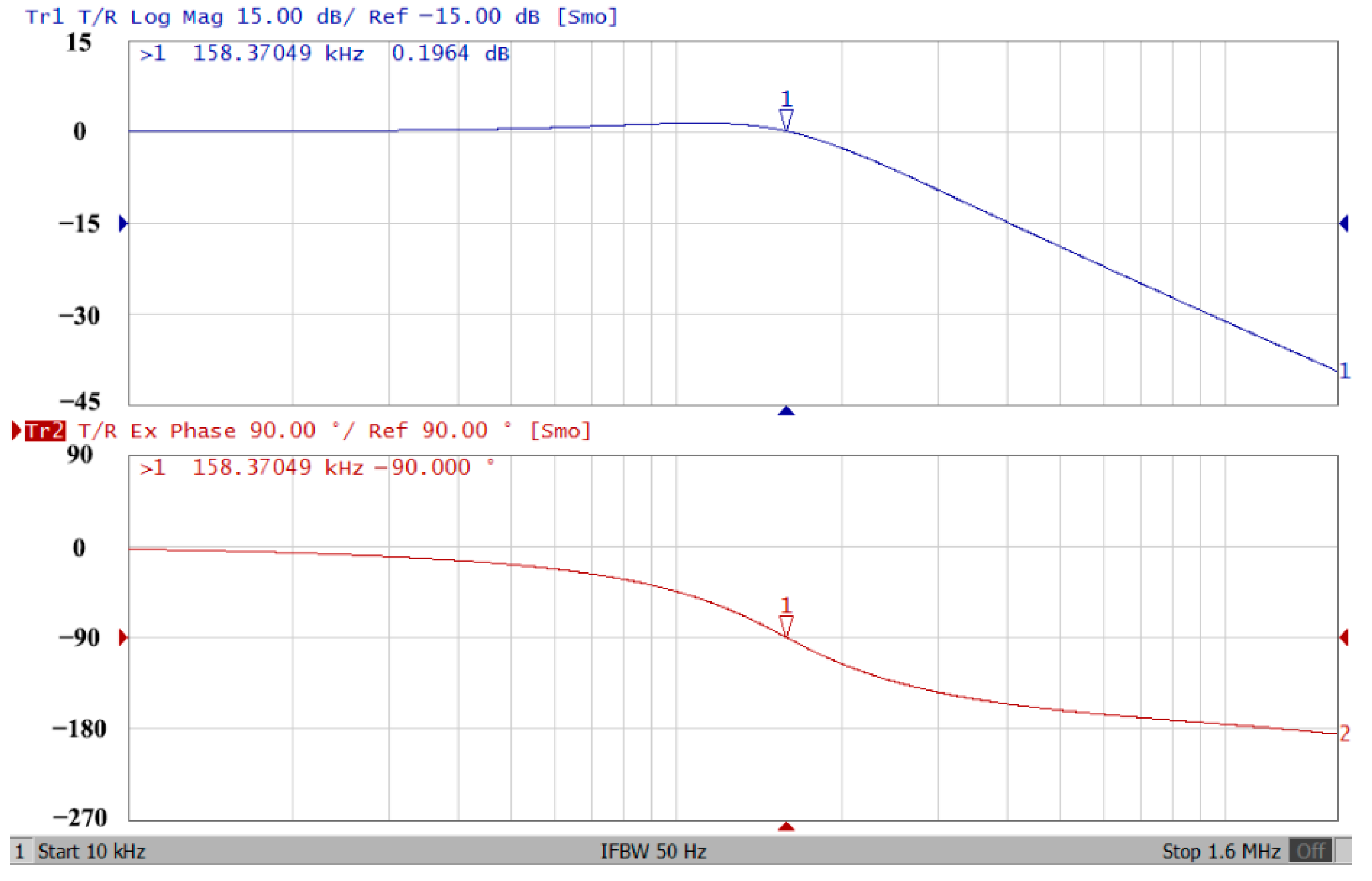
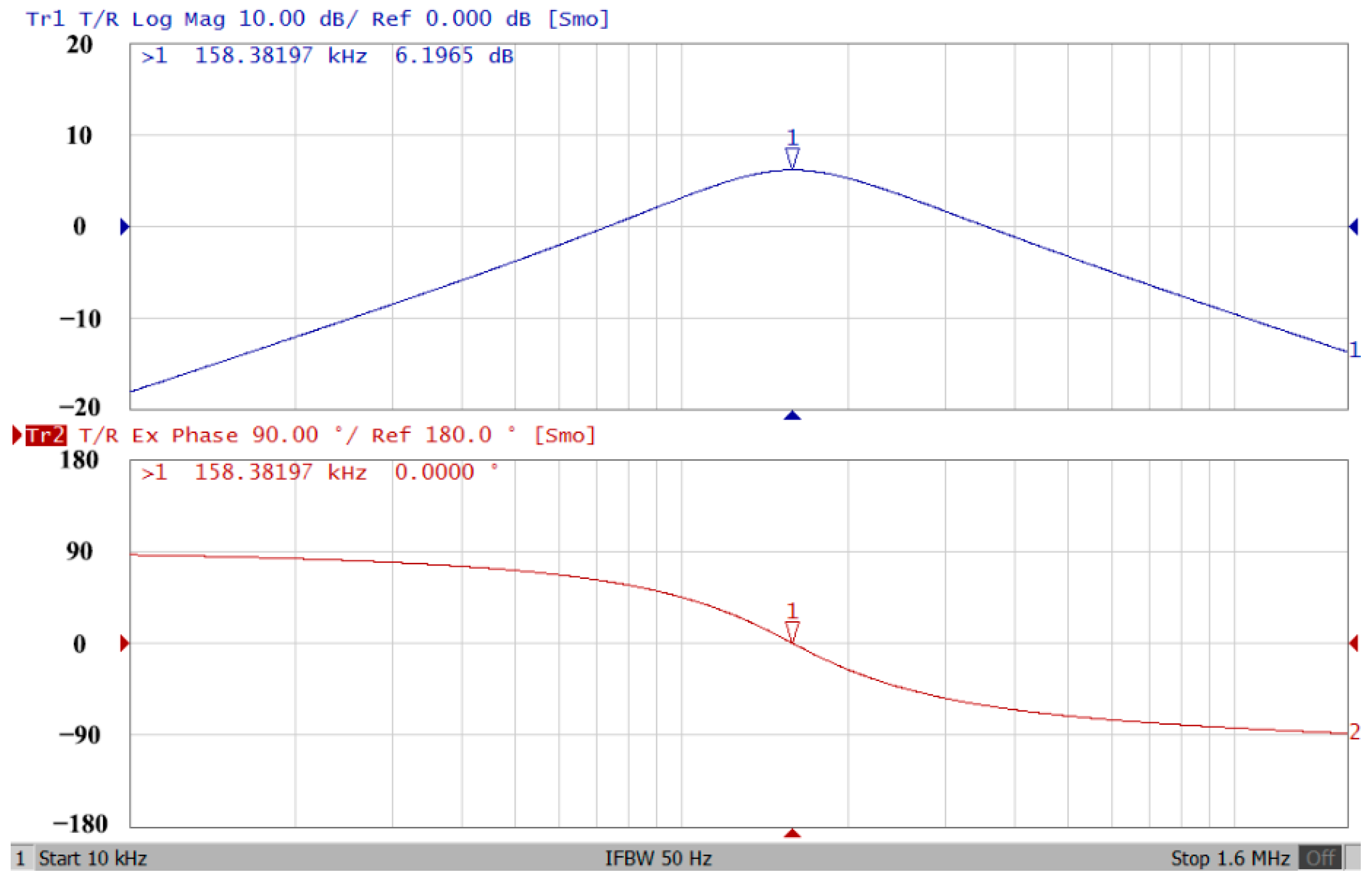
Figure 31.
Frequency-domain characteristics of the measured amplitude and phase responses of the first proposed circuit at Vo2.
Figure 31.
Frequency-domain characteristics of the measured amplitude and phase responses of the first proposed circuit at Vo2.
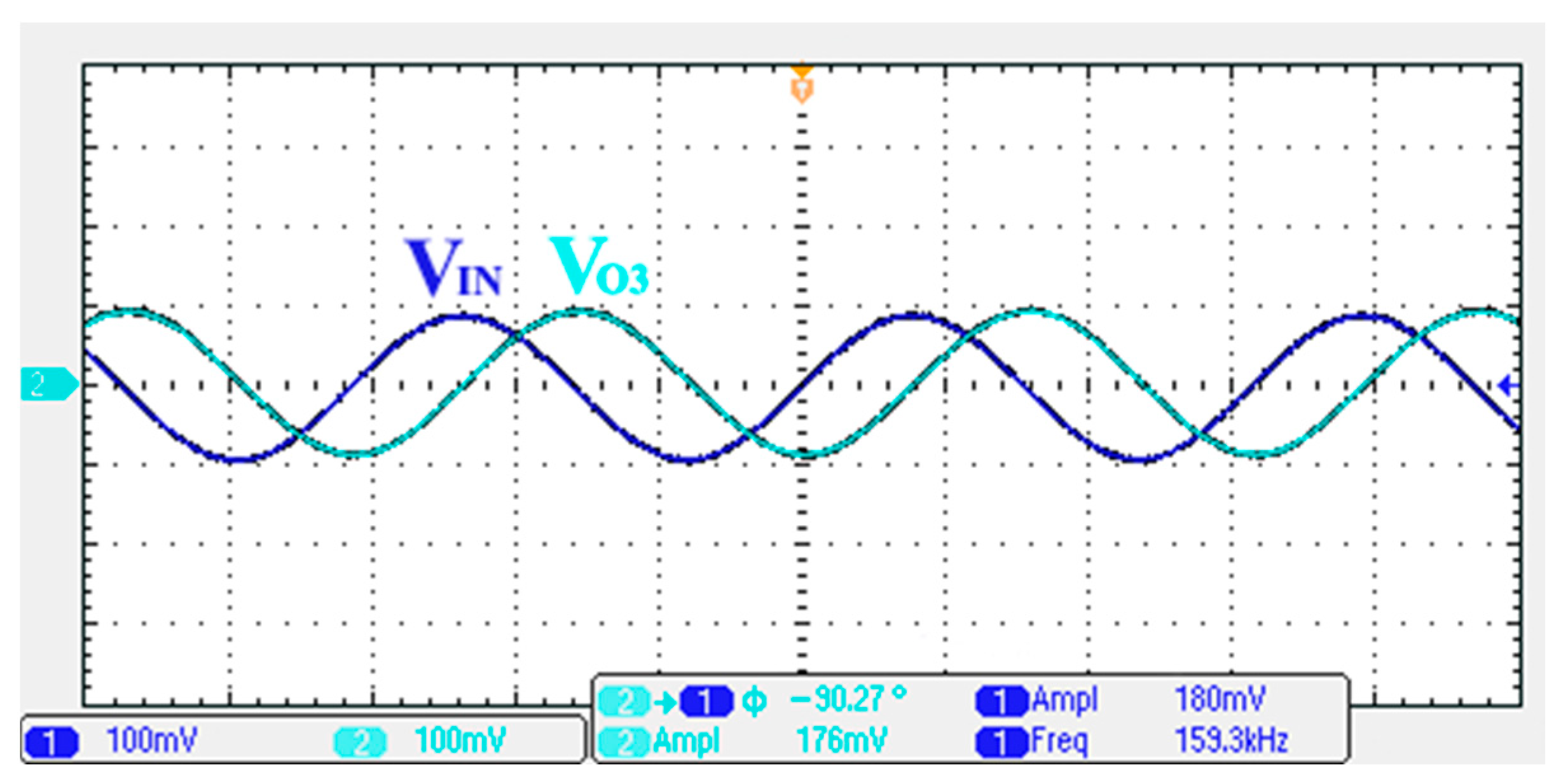
Figure 32.
Frequency-domain characteristics of the measured amplitude and phase responses of the first proposed circuit at Vo3.
Figure 32.
Frequency-domain characteristics of the measured amplitude and phase responses of the first proposed circuit at Vo3.
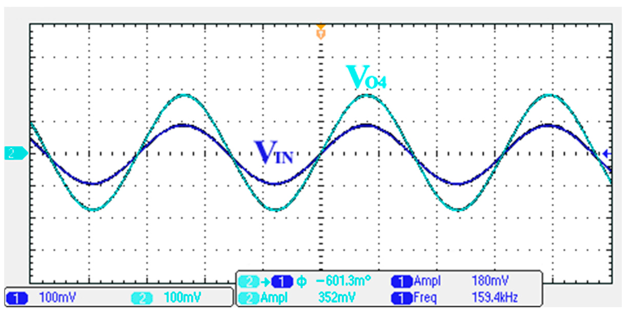
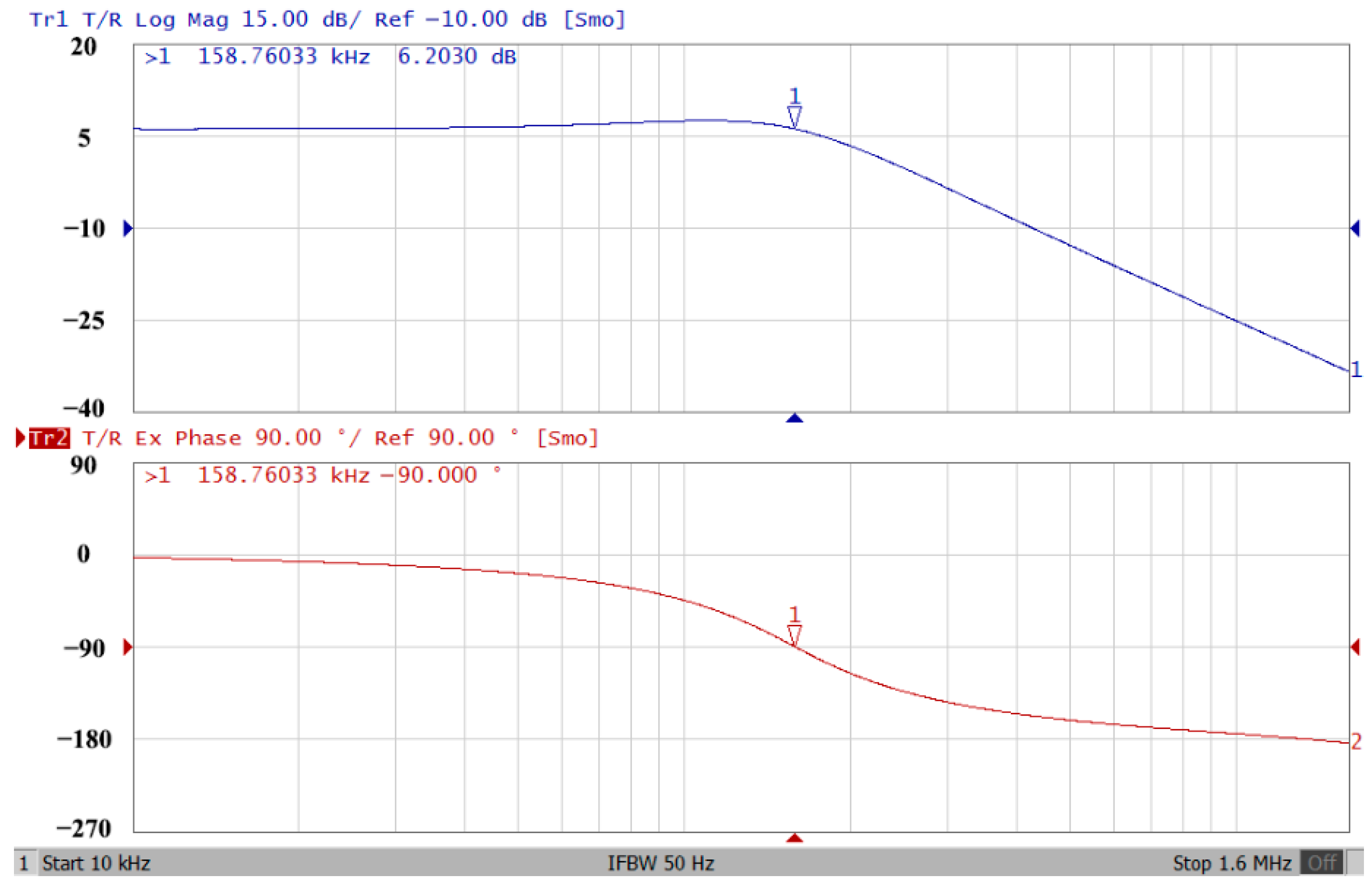
Figure 33.
Frequency-domain characteristics of the measured amplitude and phase responses of the first proposed circuit at Vo4.
Figure 33.
Frequency-domain characteristics of the measured amplitude and phase responses of the first proposed circuit at Vo4.
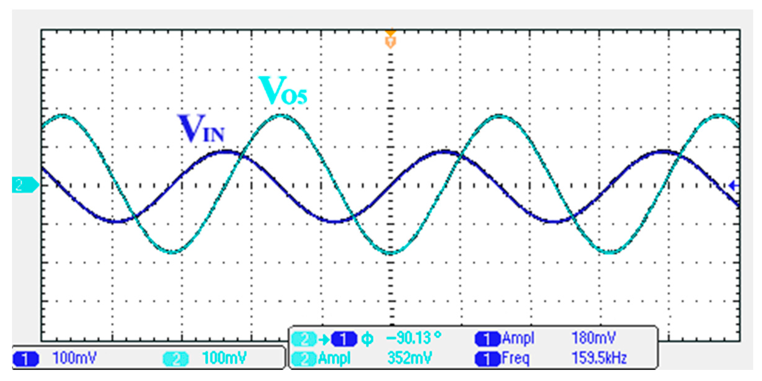
Figure 34.
Frequency-domain characteristics of the measured amplitude and phase responses of the first proposed circuit at Vo5.
Figure 34.
Frequency-domain characteristics of the measured amplitude and phase responses of the first proposed circuit at Vo5.
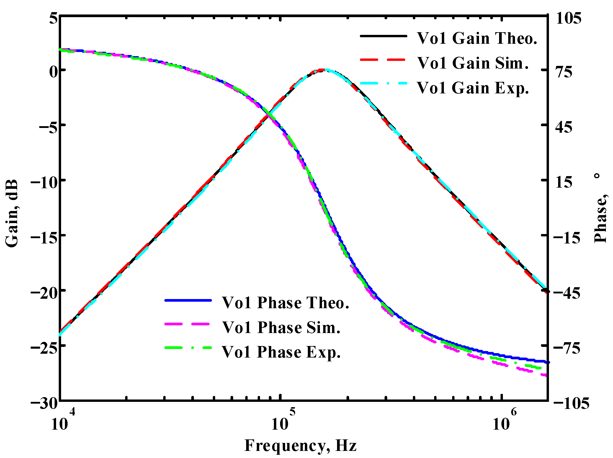
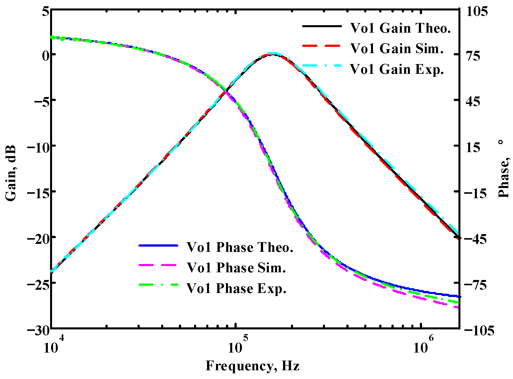
Figure 35.
Simulated, measured, and theoretical comparison results of the first proposed circuit at Vo1.
Figure 35.
Simulated, measured, and theoretical comparison results of the first proposed circuit at Vo1.
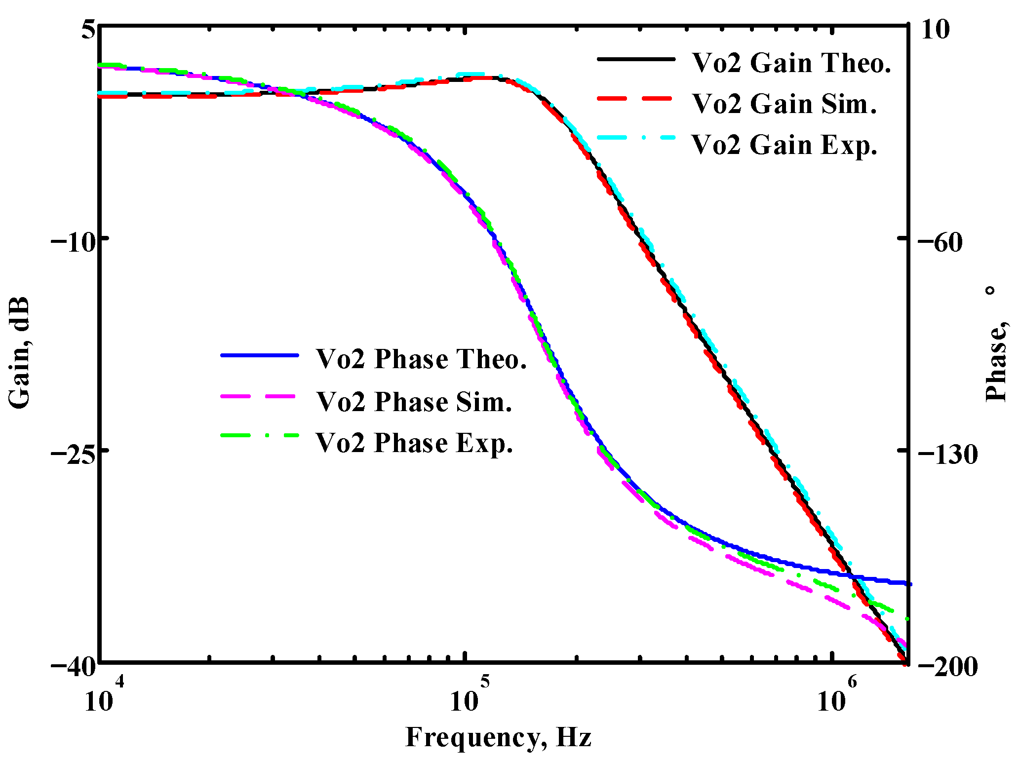
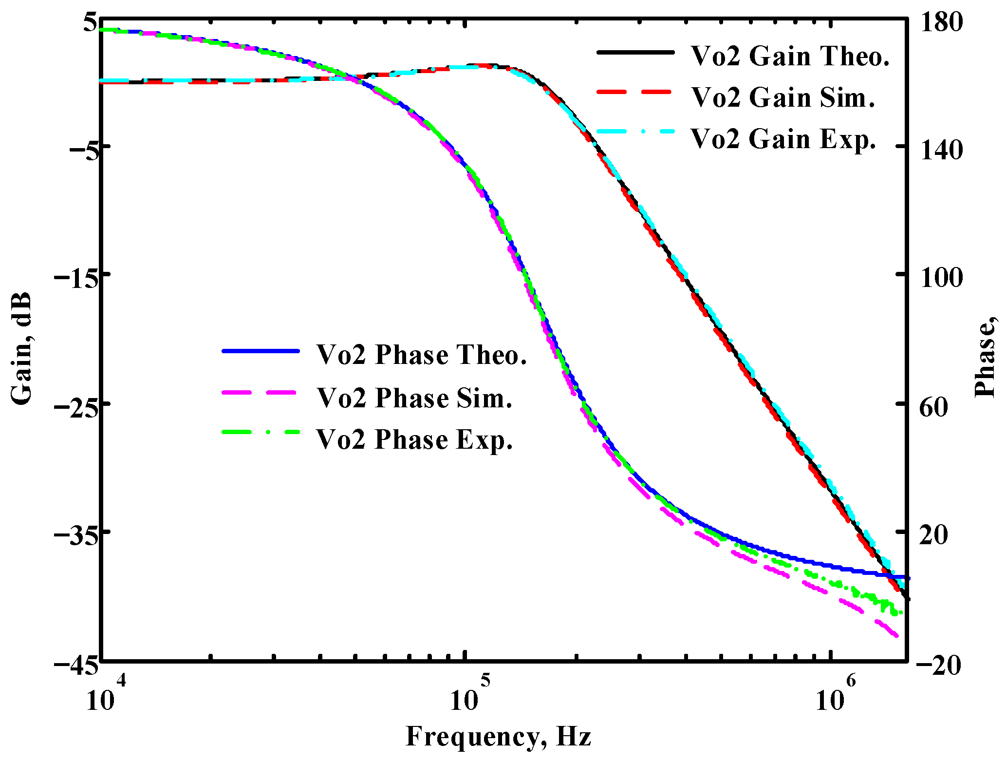
Figure 36.
Simulated, measured, and theoretical comparison results of the first proposed circuit at Vo2.
Figure 36.
Simulated, measured, and theoretical comparison results of the first proposed circuit at Vo2.
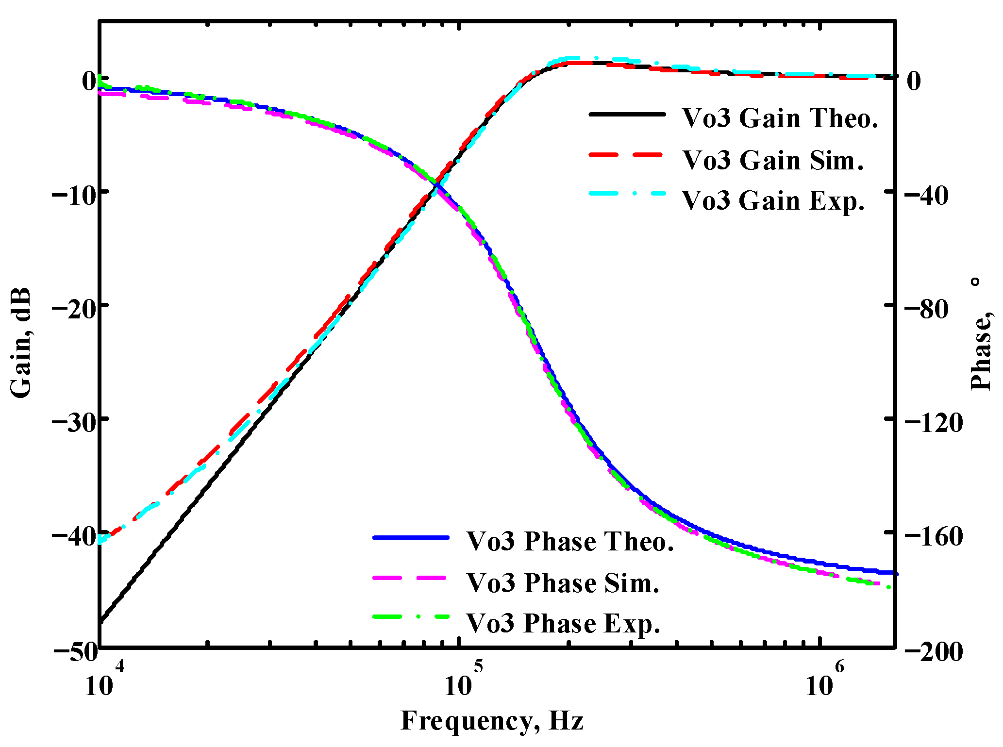
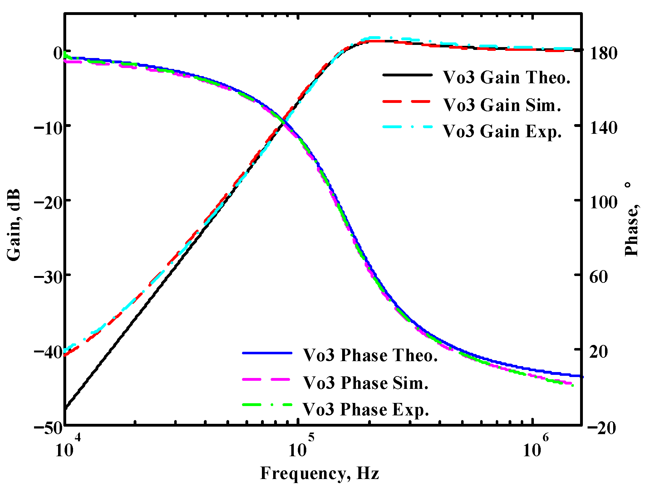
Figure 37.
Simulated, measured, and theoretical comparison results of the first proposed circuit at Vo3.
Figure 37.
Simulated, measured, and theoretical comparison results of the first proposed circuit at Vo3.
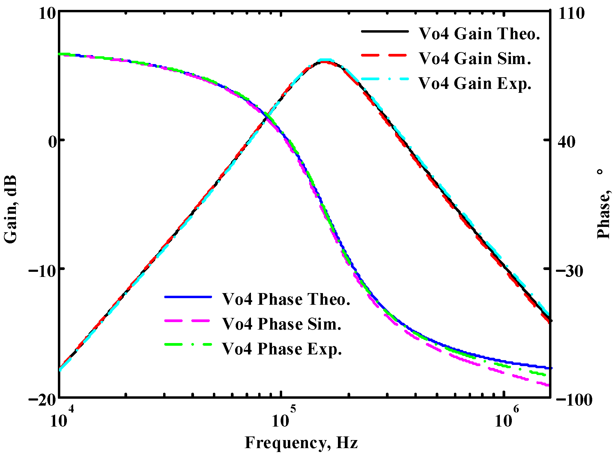
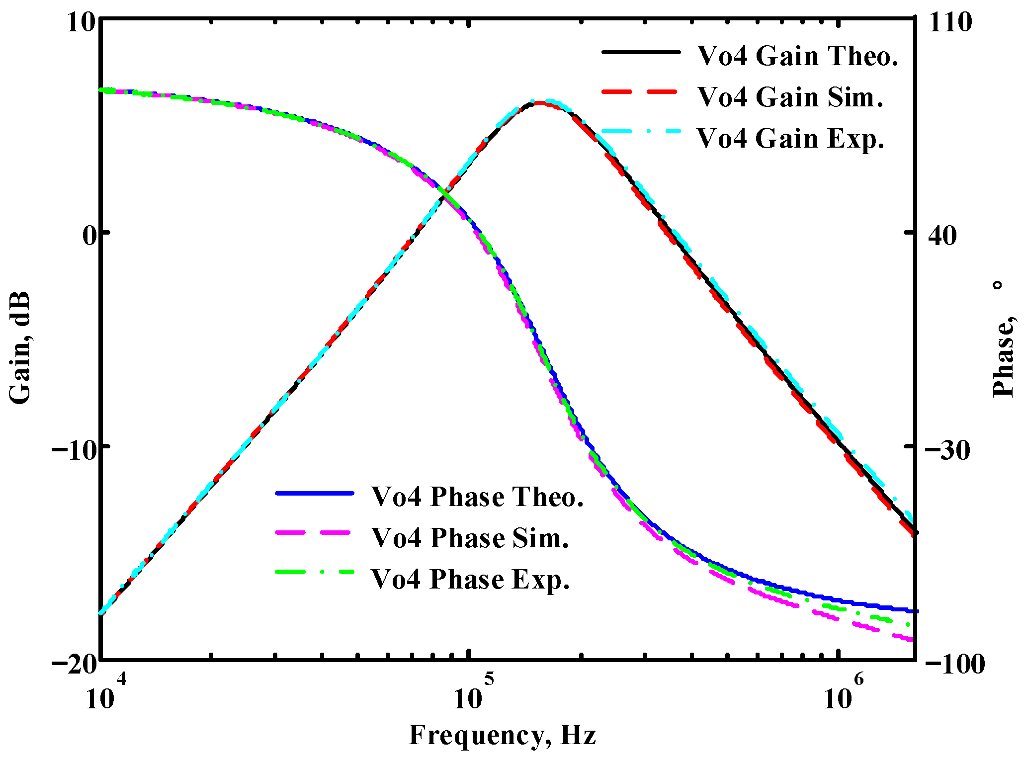
Figure 38.
Simulated, measured, and theoretical comparison results of the first proposed circuit at Vo4.
Figure 38.
Simulated, measured, and theoretical comparison results of the first proposed circuit at Vo4.
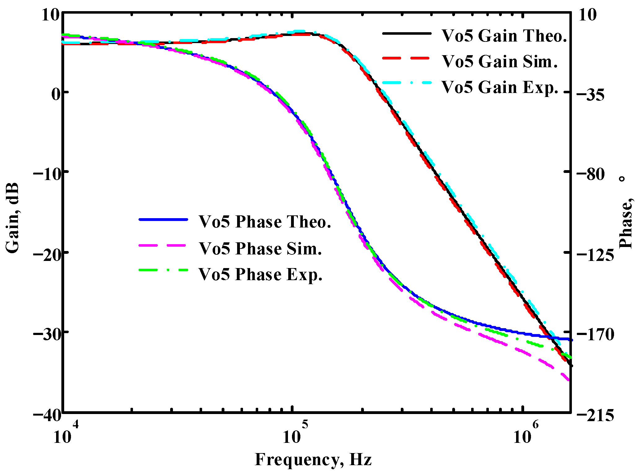
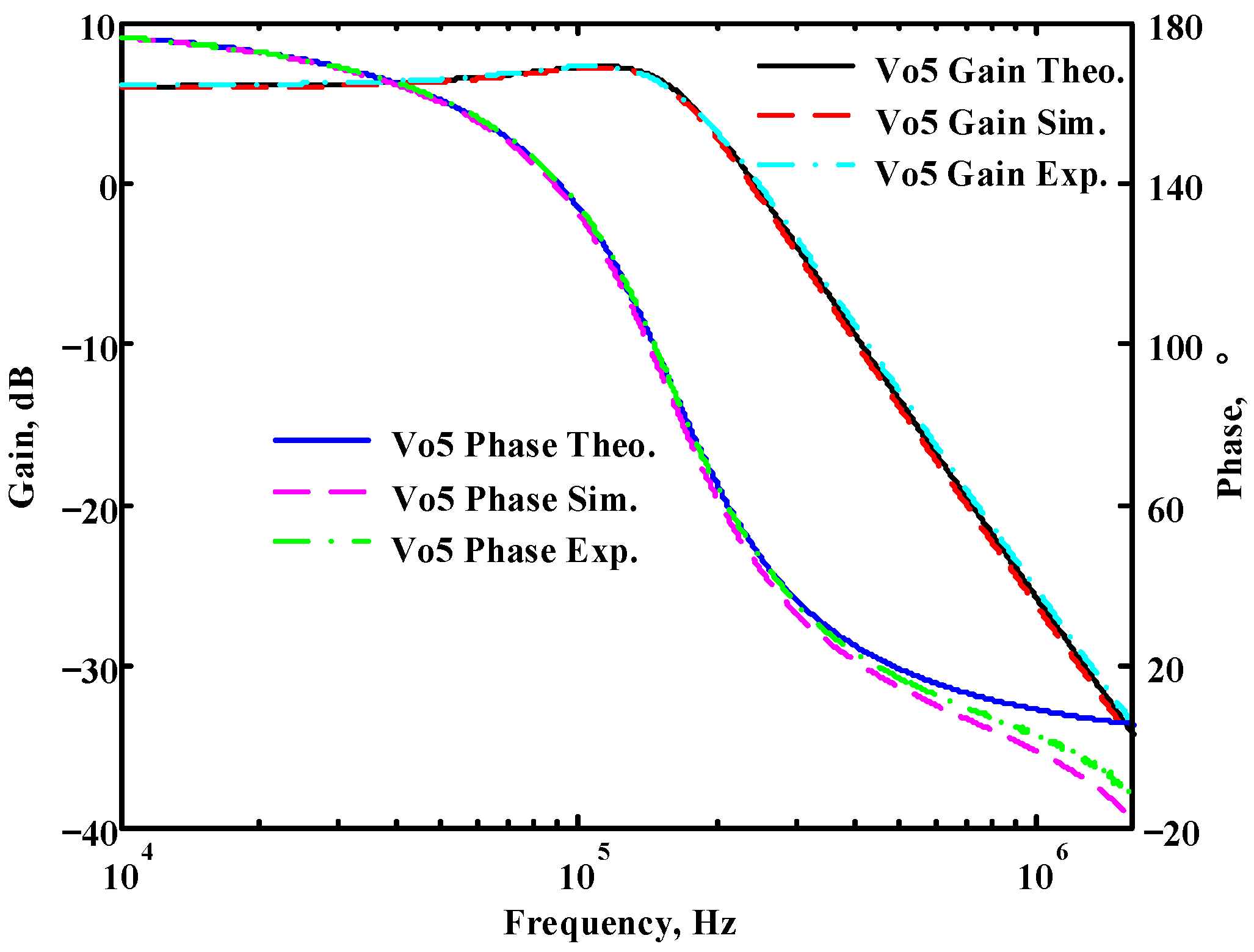
Figure 39.
Simulated, measured, and theoretical comparison results of the first proposed circuit at Vo5.
Figure 39.
Simulated, measured, and theoretical comparison results of the first proposed circuit at Vo5.
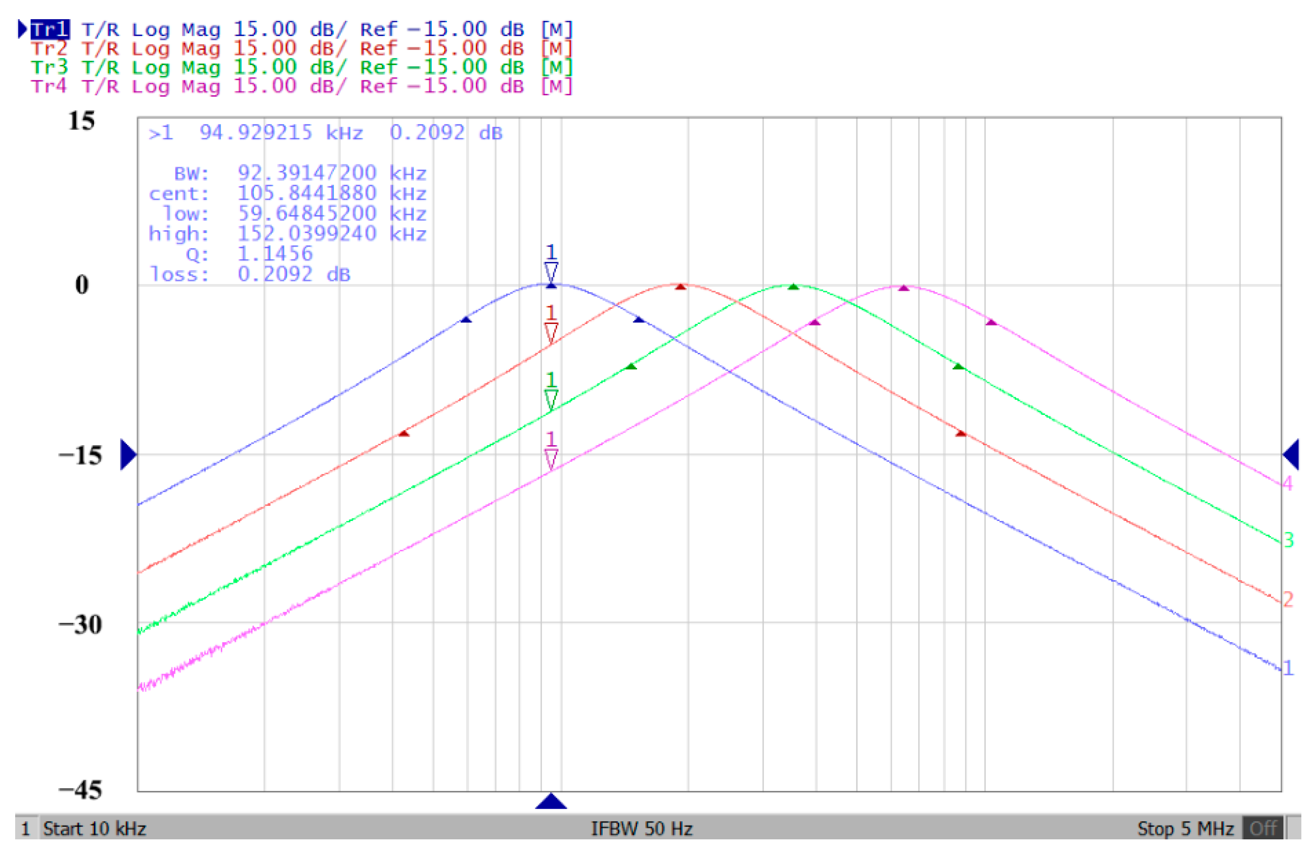
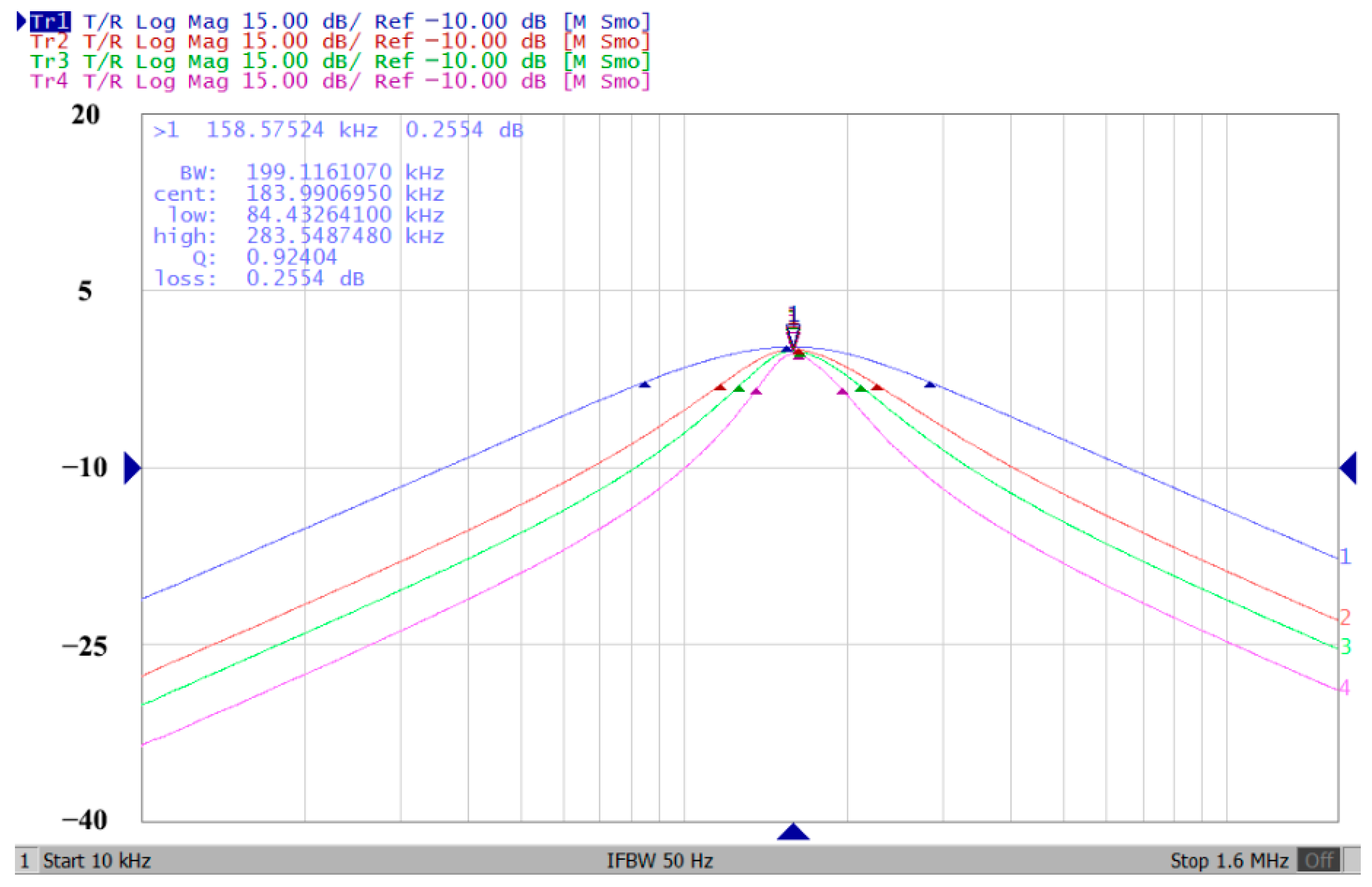
Figure 40.
Electronic tunability fo measured at Vo1 from 94.92 to 635.39 kHz for the first proposed circuit without affecting the Q value.
Figure 40.
Electronic tunability fo measured at Vo1 from 94.92 to 635.39 kHz for the first proposed circuit without affecting the Q value.
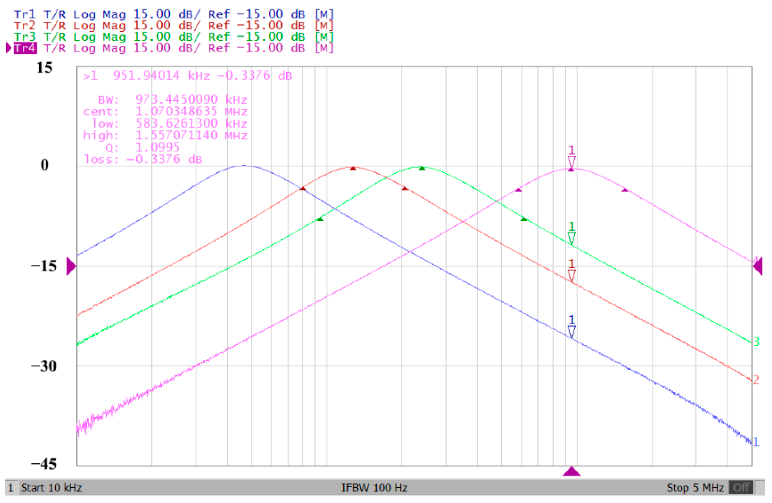
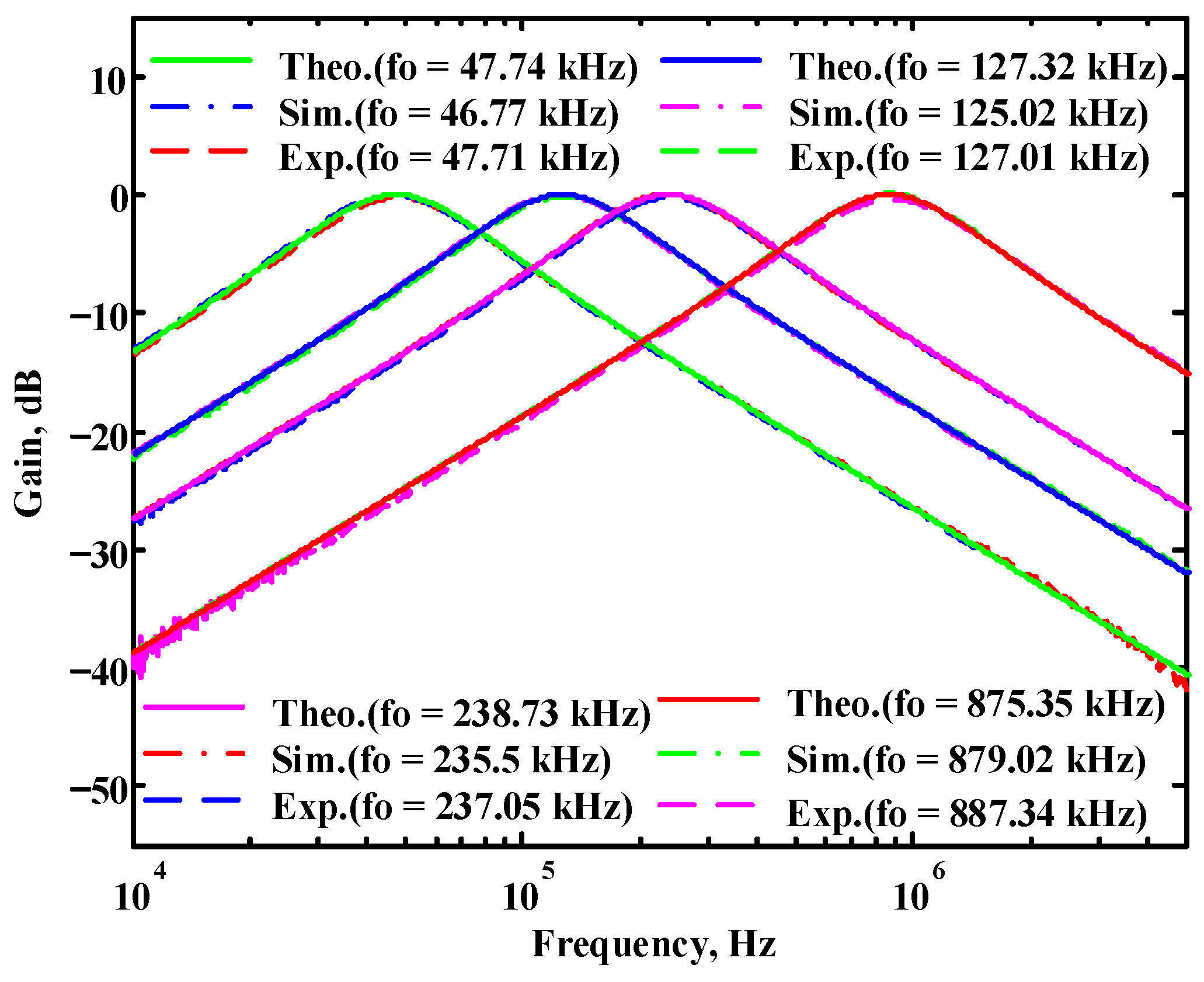
Figure 41.
Electronic tunability fo measured at Vo1 from 47.2 to 951.94 kHz for the first proposed circuit without affecting the Q value.
Figure 41.
Electronic tunability fo measured at Vo1 from 47.2 to 951.94 kHz for the first proposed circuit without affecting the Q value.
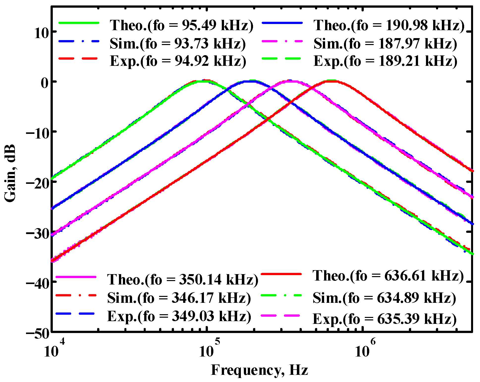
Figure 42.
Simulated, measured, and theoretical comparison results of the electronic tunability f
o at V
o1 in
Figure 40 without affecting the Q value.
Figure 42.
Simulated, measured, and theoretical comparison results of the electronic tunability f
o at V
o1 in
Figure 40 without affecting the Q value.
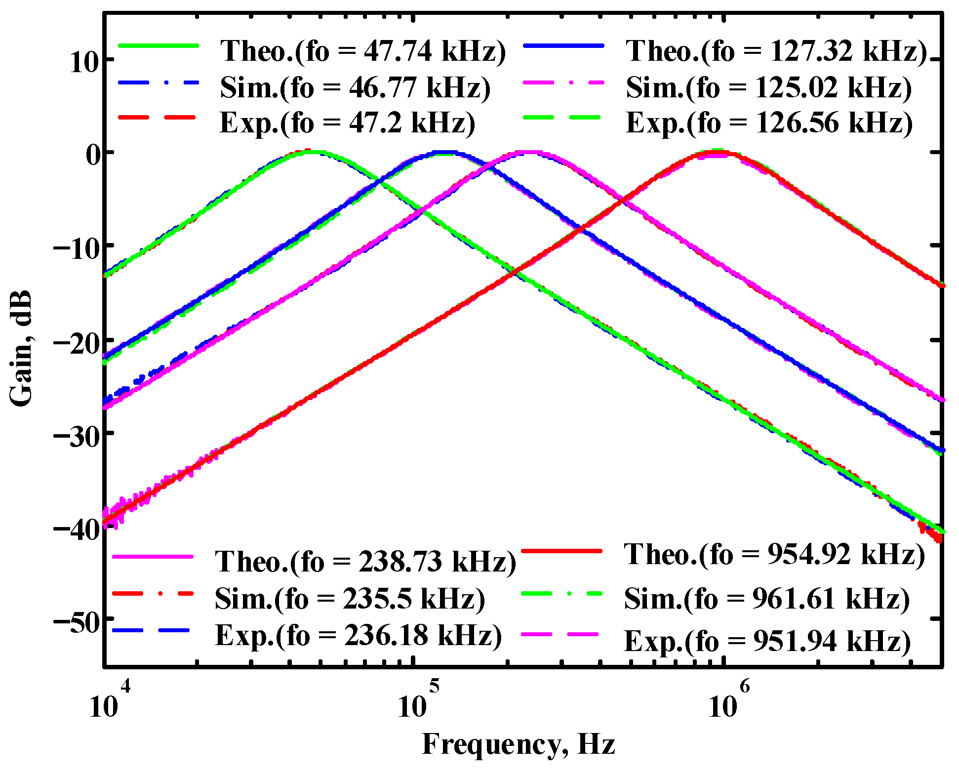
Figure 43.
Simulated, measured, and theoretical comparison results of the electronic tenability f
o at V
o1 in
Figure 41 without affecting the Q value.
Figure 43.
Simulated, measured, and theoretical comparison results of the electronic tenability f
o at V
o1 in
Figure 41 without affecting the Q value.
Figure 44.
Measured electronic tunability Q of the first proposed circuit at Vo1 without affecting the fo value.
Figure 44.
Measured electronic tunability Q of the first proposed circuit at Vo1 without affecting the fo value.
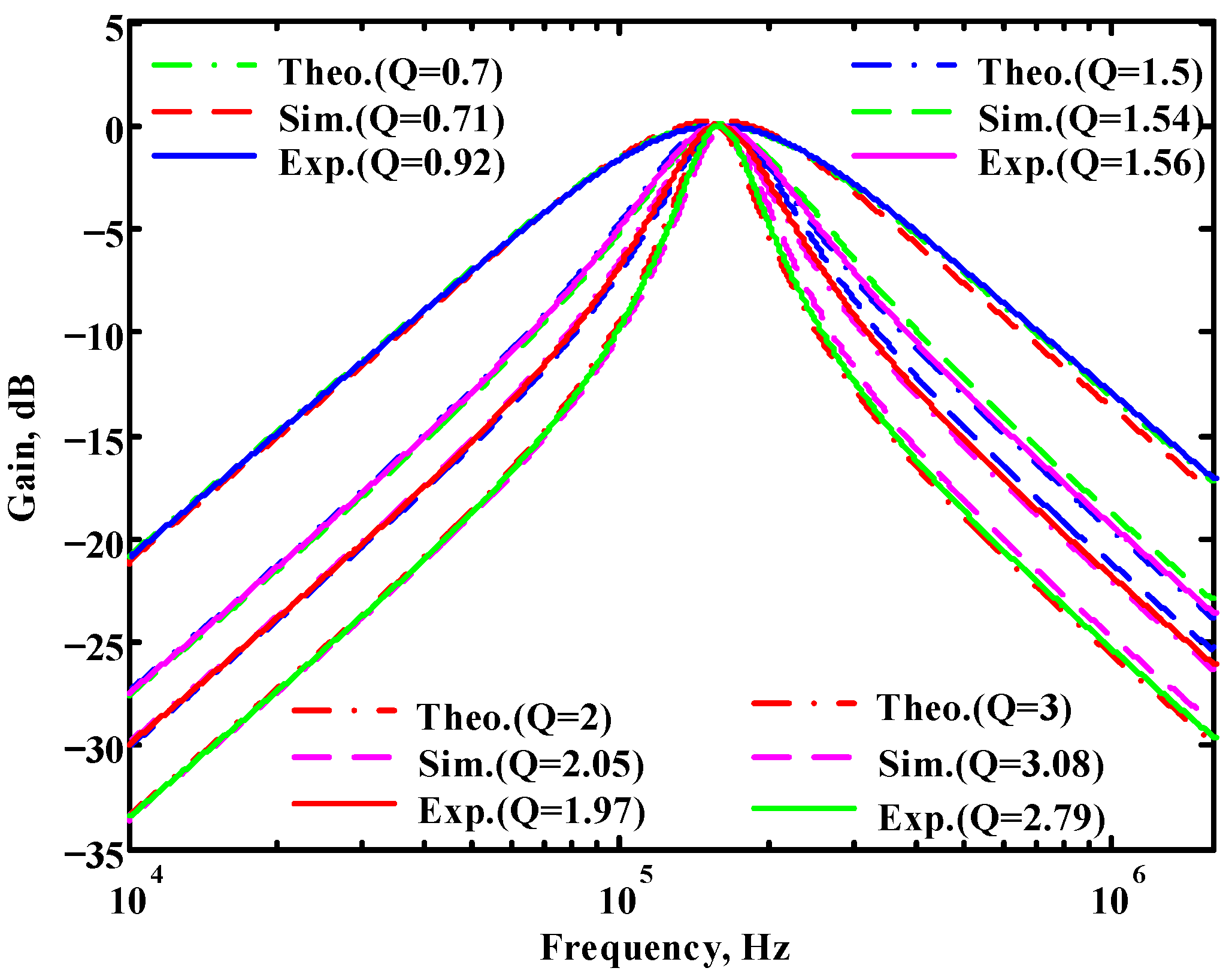
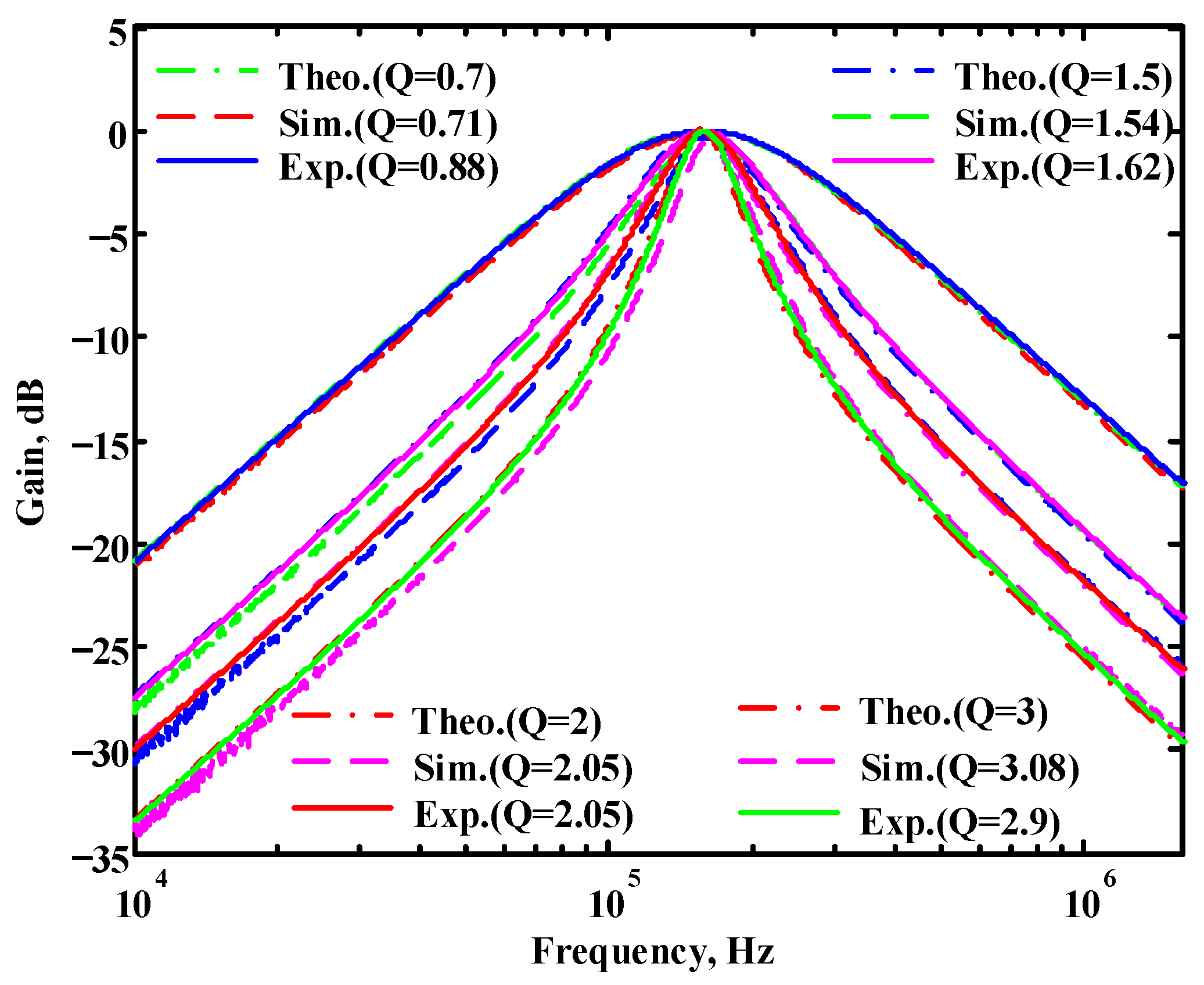
Figure 45.
Simulated, measured, and theoretical comparison results of the electronic tunability Q for the first proposed circuit at Vo1 without affecting the fo value.
Figure 45.
Simulated, measured, and theoretical comparison results of the electronic tunability Q for the first proposed circuit at Vo1 without affecting the fo value.
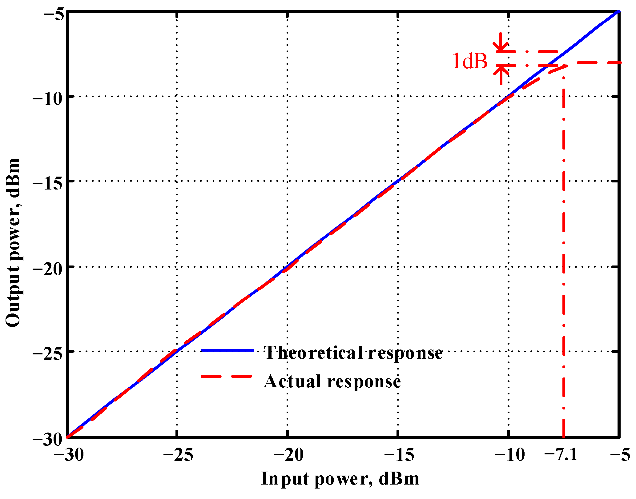
Figure 46.
Measured results of the P1dB point of the first proposed circuit at Vo1.
Figure 46.
Measured results of the P1dB point of the first proposed circuit at Vo1.
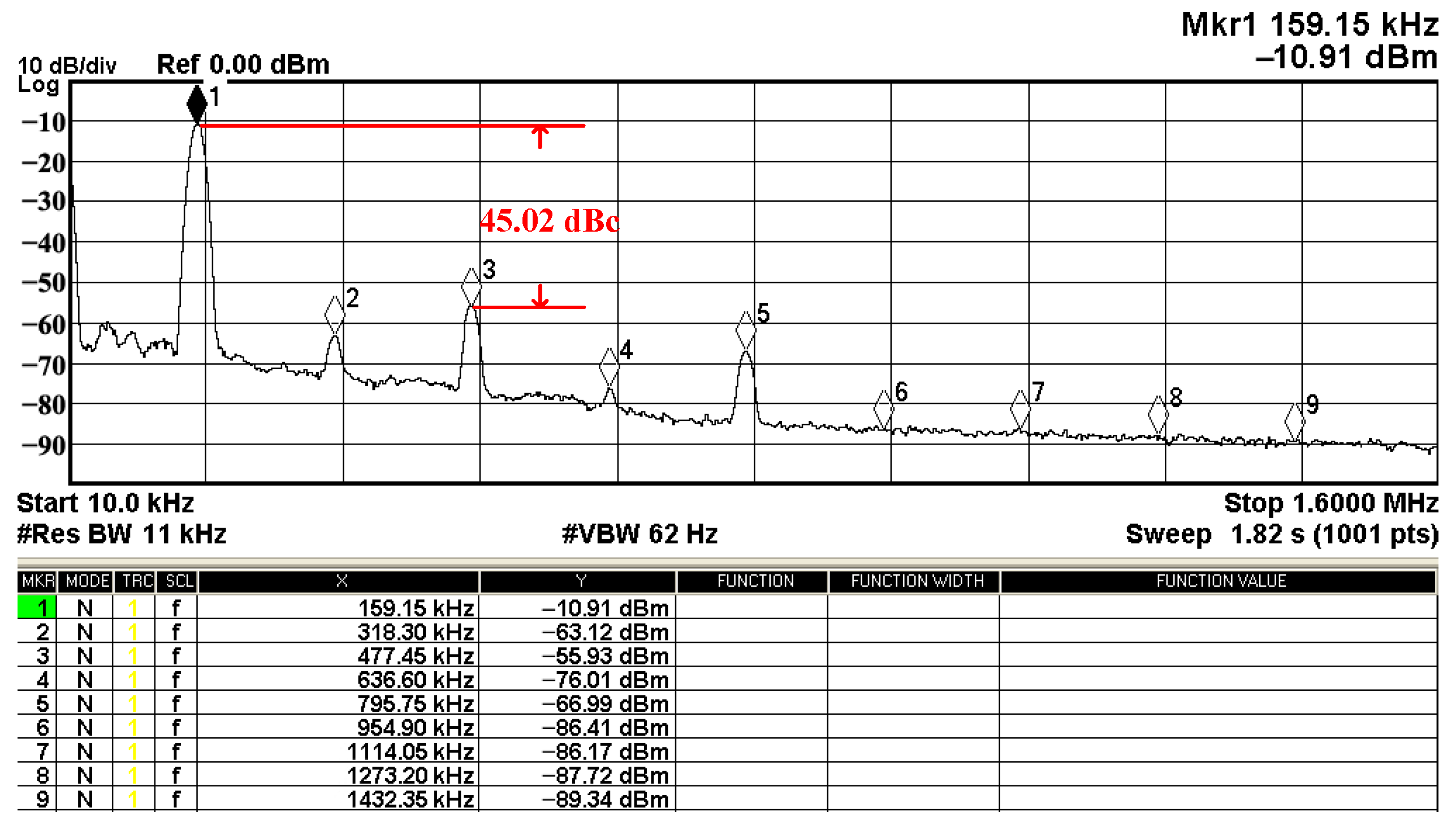
Figure 47.
Measured results of the SFDR of the first proposed circuit at Vo1.
Figure 47.
Measured results of the SFDR of the first proposed circuit at Vo1.
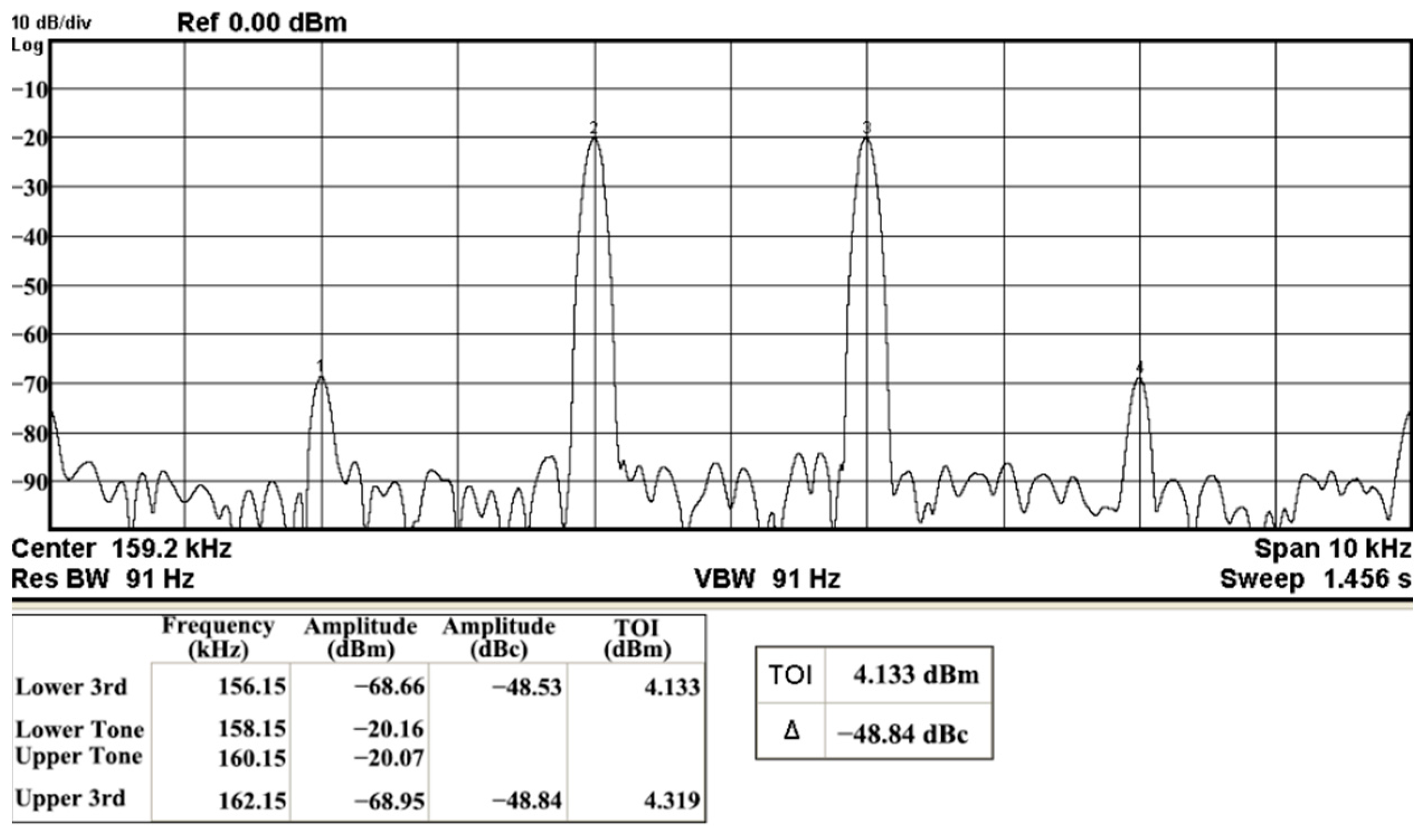
Figure 48.
Measured results of the IMD of the first proposed circuit at Vo1.
Figure 48.
Measured results of the IMD of the first proposed circuit at Vo1.
Figure 49.
Simulated gain and phase frequency response of the second proposed circuit at Vo1.
Figure 49.
Simulated gain and phase frequency response of the second proposed circuit at Vo1.
Figure 50.
Simulated gain and phase frequency response of the second proposed circuit at Vo2.
Figure 50.
Simulated gain and phase frequency response of the second proposed circuit at Vo2.
Figure 51.
Simulated gain and phase frequency response of the second proposed circuit at Vo3.
Figure 51.
Simulated gain and phase frequency response of the second proposed circuit at Vo3.
Figure 52.
Simulated gain and phase frequency response of the second proposed circuit at Vo4.
Figure 52.
Simulated gain and phase frequency response of the second proposed circuit at Vo4.
Figure 53.
Simulated gain and phase frequency response of the second proposed circuit at Vo5.
Figure 53.
Simulated gain and phase frequency response of the second proposed circuit at Vo5.
Figure 54.
Simulated gain response of the second proposed circuit at Vo1 by changing Q and keeping fo constant.
Figure 54.
Simulated gain response of the second proposed circuit at Vo1 by changing Q and keeping fo constant.
Figure 55.
Simulated gain response of the second proposed circuit at Vo1 by changing fo and keeping Q constant.
Figure 55.
Simulated gain response of the second proposed circuit at Vo1 by changing fo and keeping Q constant.
Figure 56.
Simulated gain response of the second proposed circuit at Vo2 by changing fo and keeping Q constant.
Figure 56.
Simulated gain response of the second proposed circuit at Vo2 by changing fo and keeping Q constant.
Figure 57.
Simulated gain response of the second proposed circuit at Vo3 by changing fo and keeping Q constant.
Figure 57.
Simulated gain response of the second proposed circuit at Vo3 by changing fo and keeping Q constant.
Figure 58.
Simulated temperature variation at Vo1 for the second proposed circuit.
Figure 58.
Simulated temperature variation at Vo1 for the second proposed circuit.
Figure 59.
Simulated temperature variation at Vo2 for the second proposed circuit.
Figure 59.
Simulated temperature variation at Vo2 for the second proposed circuit.
Figure 60.
Simulated temperature variation at Vo3 for the second proposed circuit.
Figure 60.
Simulated temperature variation at Vo3 for the second proposed circuit.
Figure 61.
Simulated, measured, and theoretical comparison results of the second proposed circuit at Vo1.
Figure 61.
Simulated, measured, and theoretical comparison results of the second proposed circuit at Vo1.
Figure 62.
Simulated, measured, and theoretical comparison results of the second proposed circuit at Vo2.
Figure 62.
Simulated, measured, and theoretical comparison results of the second proposed circuit at Vo2.
Figure 63.
Simulated, measured, and theoretical comparison results of the second proposed circuit at Vo3.
Figure 63.
Simulated, measured, and theoretical comparison results of the second proposed circuit at Vo3.
Figure 64.
Simulated, measured, and theoretical comparison results of the second proposed circuit at Vo4.
Figure 64.
Simulated, measured, and theoretical comparison results of the second proposed circuit at Vo4.
Figure 65.
Simulated, measured, and theoretical comparison results of the second proposed circuit at Vo5.
Figure 65.
Simulated, measured, and theoretical comparison results of the second proposed circuit at Vo5.
Figure 66.
Simulated, measured, and theoretical comparison results of the electronic tunability fo for the second proposed circuit at Vo1 without affecting the Q value.
Figure 66.
Simulated, measured, and theoretical comparison results of the electronic tunability fo for the second proposed circuit at Vo1 without affecting the Q value.
Figure 67.
Simulated, measured, and theoretical comparison results of the electronic tunability Q for the second proposed circuit at Vo1 without affecting the fo value.
Figure 67.
Simulated, measured, and theoretical comparison results of the electronic tunability Q for the second proposed circuit at Vo1 without affecting the fo value.
Figure 68.
Measured output and input characteristics of the second proposed circuit at Vo1.
Figure 68.
Measured output and input characteristics of the second proposed circuit at Vo1.
Figure 69.
Measured output and input characteristics of the second proposed circuit at Vo2.
Figure 69.
Measured output and input characteristics of the second proposed circuit at Vo2.
Figure 70.
Measured output and input characteristics of the second proposed circuit at Vo3.
Figure 70.
Measured output and input characteristics of the second proposed circuit at Vo3.
Figure 71.
Measured output and input characteristics of the second proposed circuit at Vo4.
Figure 71.
Measured output and input characteristics of the second proposed circuit at Vo4.
Figure 72.
Measured output and input characteristics of the second proposed circuit at Vo5.
Figure 72.
Measured output and input characteristics of the second proposed circuit at Vo5.
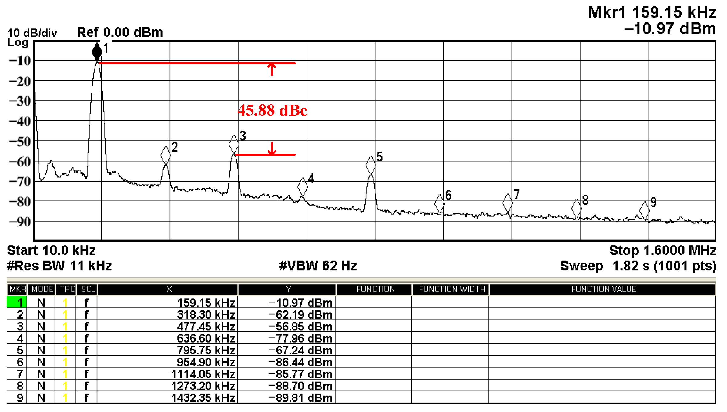
Figure 73.
Measured output spectrum of
Figure 68.
Figure 73.
Measured output spectrum of
Figure 68.
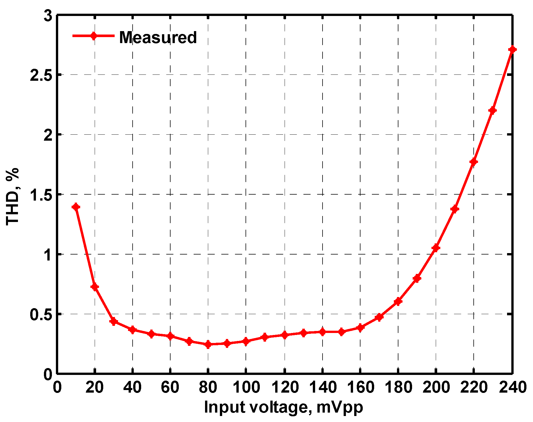
Figure 74.
Measured THD of the second proposed circuit at V
o1 in
Figure 6 versus peak-to-peak input voltage signal at 159.15 kHz.
Figure 74.
Measured THD of the second proposed circuit at V
o1 in
Figure 6 versus peak-to-peak input voltage signal at 159.15 kHz.
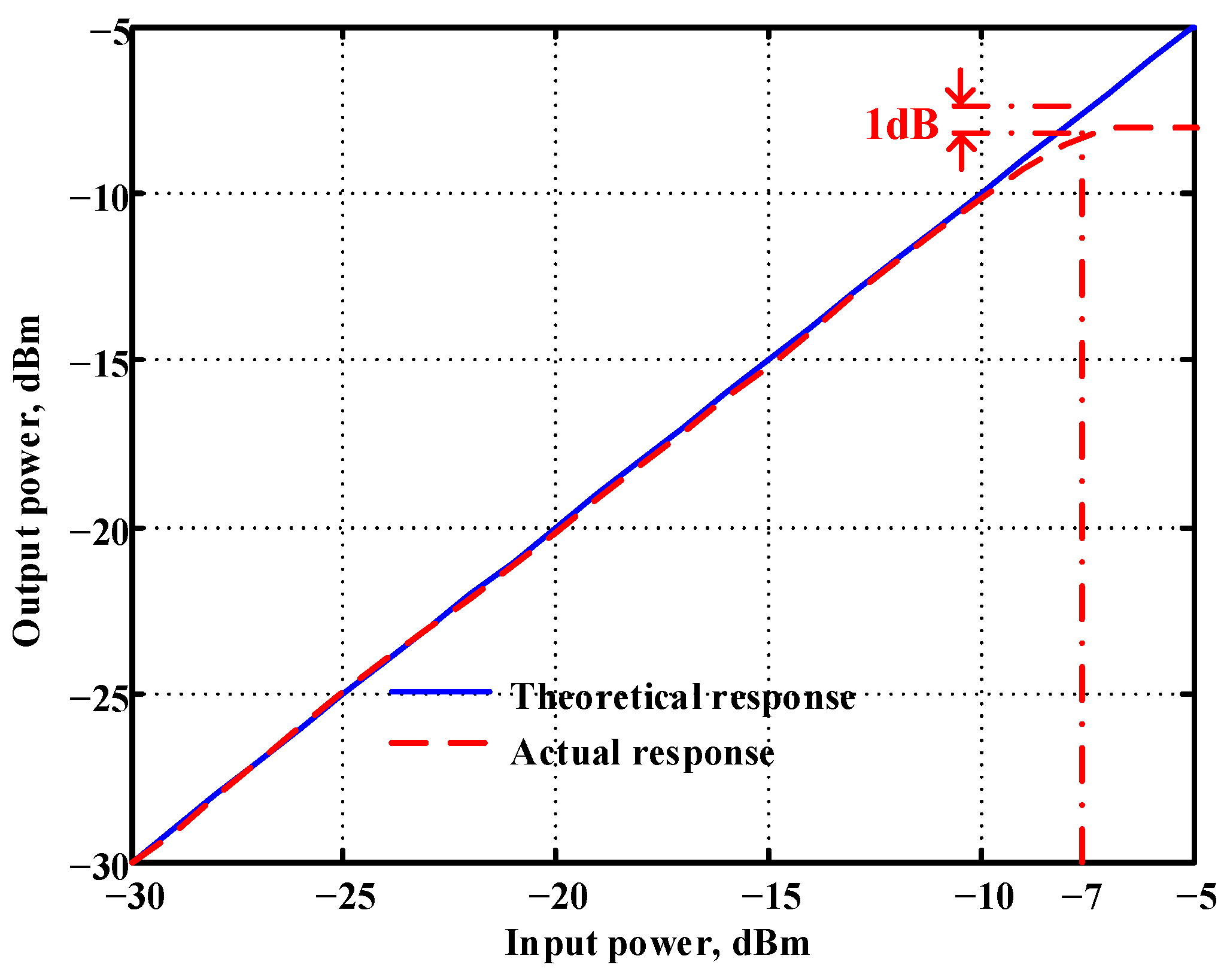
Figure 75.
Measured results of the P1dB point of the second proposed circuit at Vo1.
Figure 75.
Measured results of the P1dB point of the second proposed circuit at Vo1.
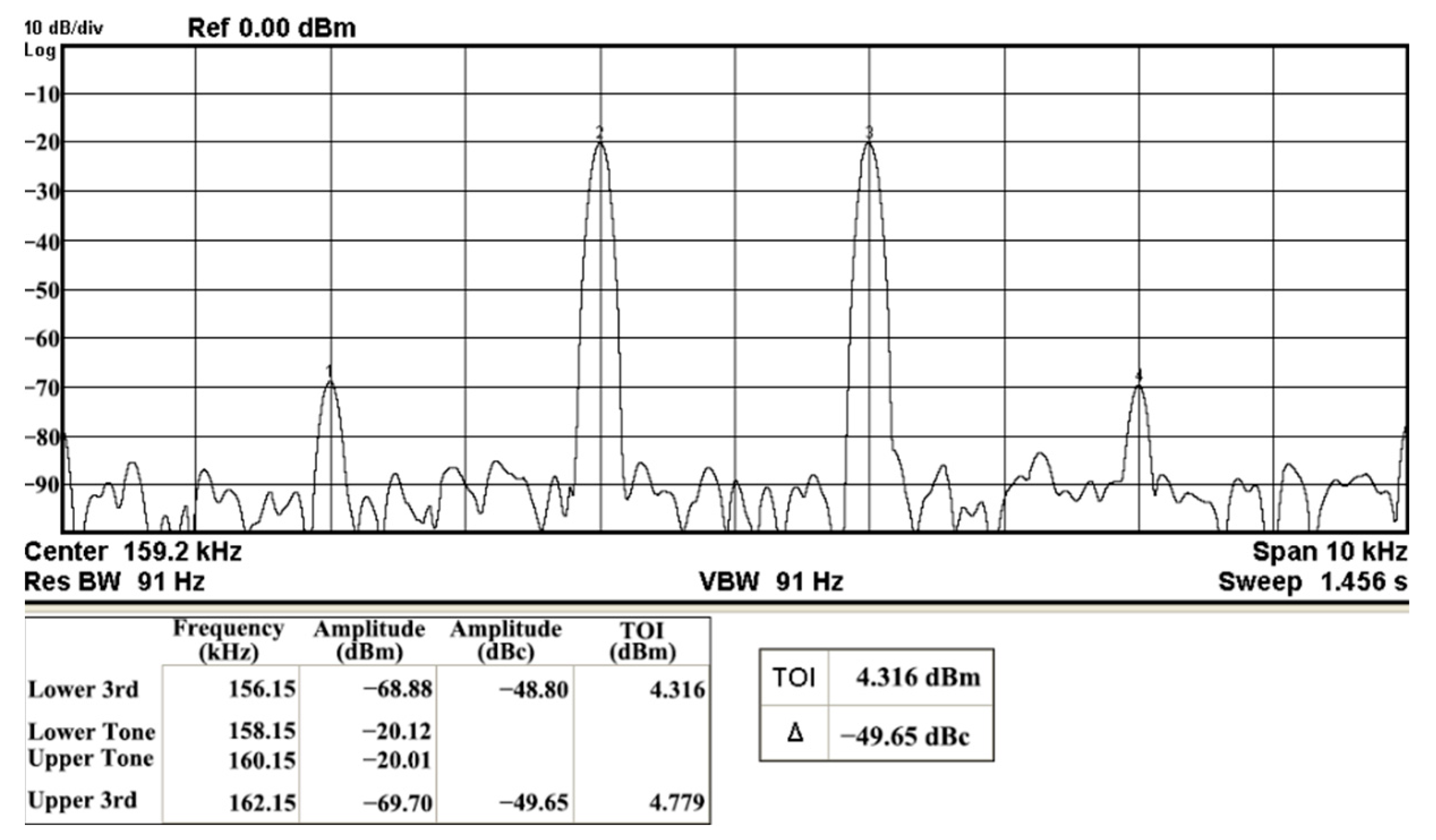
Figure 76.
Measured results of the IMD3 of the second proposed circuit at Vo1.
Figure 76.
Measured results of the IMD3 of the second proposed circuit at Vo1.
Table 1.
Comparison of recent electronically tunable VM second-order multifunction filter specifications.
Table 1.
Comparison of recent electronically tunable VM second-order multifunction filter specifications.
| Ref. | ABB and Passive Elements Used | No. of Commercial ICs Realized | No. of Filtering Functions at the Same Time | No. of Low Output Impedance Filtering Functions Used | Only High-Input Impedance Used | Only Two Grounded Capacitors Used | Simultaneous Realization of Filtering Functions | Independent Gain-Controlled Filtering Functions | Orthogonal Electronic Control of Q and fo | Independent Electronic Control Q without Affecting fo | Q-Value or Q Tuning Range | Pole Frequency fo or fo Tuning Range (kHz) |
|---|
| ABB | Passive |
|---|
| [22] | 4 CCII | 2C + 4R | 4 | 5 | 0 | yes | yes | LPF, BPF, HPF, BRF, APF a | no | no | no | <5 | 15 |
| [23] | 3 CFA | 2C + 4R | 3 | 3 | 3 | yes | yes | LPF, BPF, BRF | no | no | no | 1.1–4 | 49–197 |
| [24] | 3 CFA | 2C + 4R | 3 | 3 | 3 | yes | yes | LPF, BPF, HPF | no | no | no | 0.6–1.6 | 86–170 |
| [25] | 4 CFA in filter 1a | 2C + 5R + 2SW | 4 | 4 | 4 | yes | yes | LPF, BPF, BRF, HPF/APF | no | no | no | 0.3–3.2 | 150 |
| [25] | 4 CFA in filter 1b | 2C + 6R + 2SW | 4 | 4 | 4 | yes | yes | LPF, BPF, BRF, HPF/APF | no | no | no | <0.7 | 22–210 |
| [25] | 4 CFA in filter 1c | 2C + 6R + 1SW | 4 | 4 | 4 | yes | yes | LPF, BPF, BRF, HPF/APF | no | no | no | 0.3–3.3 | 22–210 |
| [26] | 3 VDDDA | 2C + 1R | 5 | 6 | 3 | yes | yes | LPF, 2 BPF, HPF, BRF, APF | no | yes | yes | 0.3–26.6 | 1047 |
| [27] | 3 VDDDA | 2C + 1R | 5 | 5 | 2 | yes | yes | LPF, BPF, HPF, BRF, APF | no | yes | yes | 1–4.5 | 625–1500 |
| [28] | 2 VD-DIBA | 2C + 2R | 4 | 4 | 2 | yes | yes | LPF, BPF, HPF, BRF | no | no | no | 2–5 | 66–144 |
| [29] | 5 OTA | 2C | 5 | 3 | 0 | yes | yes | LPF, BPF, BRF | no | yes | yes | 1–3 | 156–472 |
| [30] | 5 OTA | 2C | 5 | 3 | 0 | yes | yes | LPF, BPF, BRF | no | yes | yes | 1–2.9 | 107–284 |
| [31] | 4 OTA | 2C | 5 | 3 | 0 | yes | yes | LPF, BPF, BRF | no | yes | yes | 1–1.7 | 106–213 |
| [32] | 3 LT1228 in filter 2a | 2C + 3R | 3 | 3 | 2 | yes | yes | 3 BPF | 1 BPF | no | no | 1–2.9 | 161 |
| [32] | 3 LT1228 in filter 3a | 2C + 3R | 3 | 3 | 2 | yes | yes | 3 BPF | 1 BPF | no | no | 1–2.9 | 165 |
| [33] | 3 LT1228 | 2C + 4R | 3 | 3 | 2 | no | yes | HPF, BPF, LPF | no | yes | yes | 0.4–1.7 | 100–373 |
| [34] | 2 LT1228 in filter 1 | 2C + 3R | 2 | 3 | 2 | no | yes | HPF a, BPF a, LPF a | no | no | no | <1.6 | 135–826 |
| [34] | 2 LT1228 in filter 2 | 2C + 3R | 2 | 3 | 2 | no | yes | HPF a, BPF a, LPF a | no | no | no | <1.6 | 44.3–275 |
| [35] | 2 LT1228 in filter 2a | 2C + 5R | 2 | 3 | 2 | no | yes | HPF a, BPF a, LPF a | no | no | no | 0.9–4.5 | 57–205 |
| [35] | 2 LT1228 in filter 2b | 2C + 5R | 2 | 3 | 2 | no | yes | HPF a, BPF a, LPF a | no | no | no | 0.9–4.5 | 99 |
| Circuit 1 | 3 LT1228 | 2C + 5R | 3 | 5 | 3 | yes | yes | HPF, 2 BPF, 2 LPF | 1 LPF, 1 BPF | yes | yes | 0.7–6 | 46–961 |
| Circuit 2 | 3 LT1228 | 2C + 5R | 3 | 5 | 3 | yes | yes | 1 HPF, 2 BPF, 2 LPF | 1 LPF, 1 BPF | yes | yes | 0.7–6 | 46–879 |
Table 2.
Time domain characteristics of the output phase errors of the first proposed filter measured at 159.15 kHz.
Table 2.
Time domain characteristics of the output phase errors of the first proposed filter measured at 159.15 kHz.
| Output Terminal | Operating Pole Phase | Output Phase Error |
|---|
| Theoretical | Measured |
|---|
| Vo1 | 0° | −0.143° | −0.143° |
| Vo2 | −90° | −90.97° | −0.97° |
| Vo3 | −90° | −90.27° | −0.27° |
| Vo4 | 0° | −0.601° | −0.601° |
| Vo5 | −90° | −90.13° | −0.13° |
Table 3.
Frequency-domain characteristics of the pole frequency error measured at ideal pole phase for the first proposed circuit.
Table 3.
Frequency-domain characteristics of the pole frequency error measured at ideal pole phase for the first proposed circuit.
| Output Terminal | Filter Pole Frequency | Percentage Error of the Pole Frequency |
|---|
| Theoretical | Simulated | Measured | Simulated | Measured |
|---|
| Vo1 | 159.15 kHz | 155.59 kHz | 157.2 kHz | −2.23% | −1.22% |
| Vo2 | 159.15 kHz | 155.23 kHz | 158.37 kHz | −2.46% | −0.49% |
| Vo3 | 159.15 kHz | 155.59 kHz | 157.58 kHz | −2.23% | −0.98% |
| Vo4 | 159.15 kHz | 155.23 kHz | 158.38 kHz | −2.46% | −0.48% |
| Vo5 | 159.15 kHz | 154.88 kHz | 158.76 kHz | −2.68% | −0.24% |
Table 4.
Summary of the measured performance of the first proposed VM LT1228-based second-order multifunction filter.
Table 4.
Summary of the measured performance of the first proposed VM LT1228-based second-order multifunction filter.
| Factor |
|---|
| Power Supply (V) | PD (W) | Pole Frequency (kHz) | Pole Frequency Tuning Range (kHz) | P1dB (dBm) | IMD3 (dBc) | TOI (dBm) | SFDR (dBc) |
|---|
| ±15 | 0.69 | 157.2 | 47.2–951.94 | −7.1 | −48.84 | 4.133 | 45.02 |
Table 5.
Frequency-domain characteristics of the pole frequency error measured at ideal pole phase for the second proposed circuit.
Table 5.
Frequency-domain characteristics of the pole frequency error measured at ideal pole phase for the second proposed circuit.
| Output Terminal | Filter Pole Frequency | Percentage Error of the Pole Frequency |
|---|
| Theoretical | Simulated | Measured | Simulated | Measured |
|---|
| Vo1 | 159.15 kHz | 155.59 kHz | 157.55 kHz | −2.23% | −1% |
| Vo2 | 159.15 kHz | 155.23 kHz | 158.22 kHz | −2.46% | −0.58% |
| Vo3 | 159.15 kHz | 155.59 kHz | 156.67 kHz | −2.23% | −1.55% |
| Vo4 | 159.15 kHz | 155.23 kHz | 157.71 kHz | −2.46% | −0.9% |
| Vo5 | 159.15 kHz | 154.88 kHz | 158.98 kHz | −2.68% | −0.1% |
Table 6.
Time-domain characteristics of the output phase error measured for the second proposed circuit at an operating pole frequency of 159.15 kHz.
Table 6.
Time-domain characteristics of the output phase error measured for the second proposed circuit at an operating pole frequency of 159.15 kHz.
| Output Terminal | Operating Pole Phase | Output Phase Error |
|---|
| Theoretical | Measured |
|---|
| Vo1 | 0° | −0.544° | −0.544° |
| Vo2 | 90° | 90.41° | 0.41° |
| Vo3 | 90° | 88.08° | −1.92° |
| Vo4 | 0° | −0.401° | −0.401° |
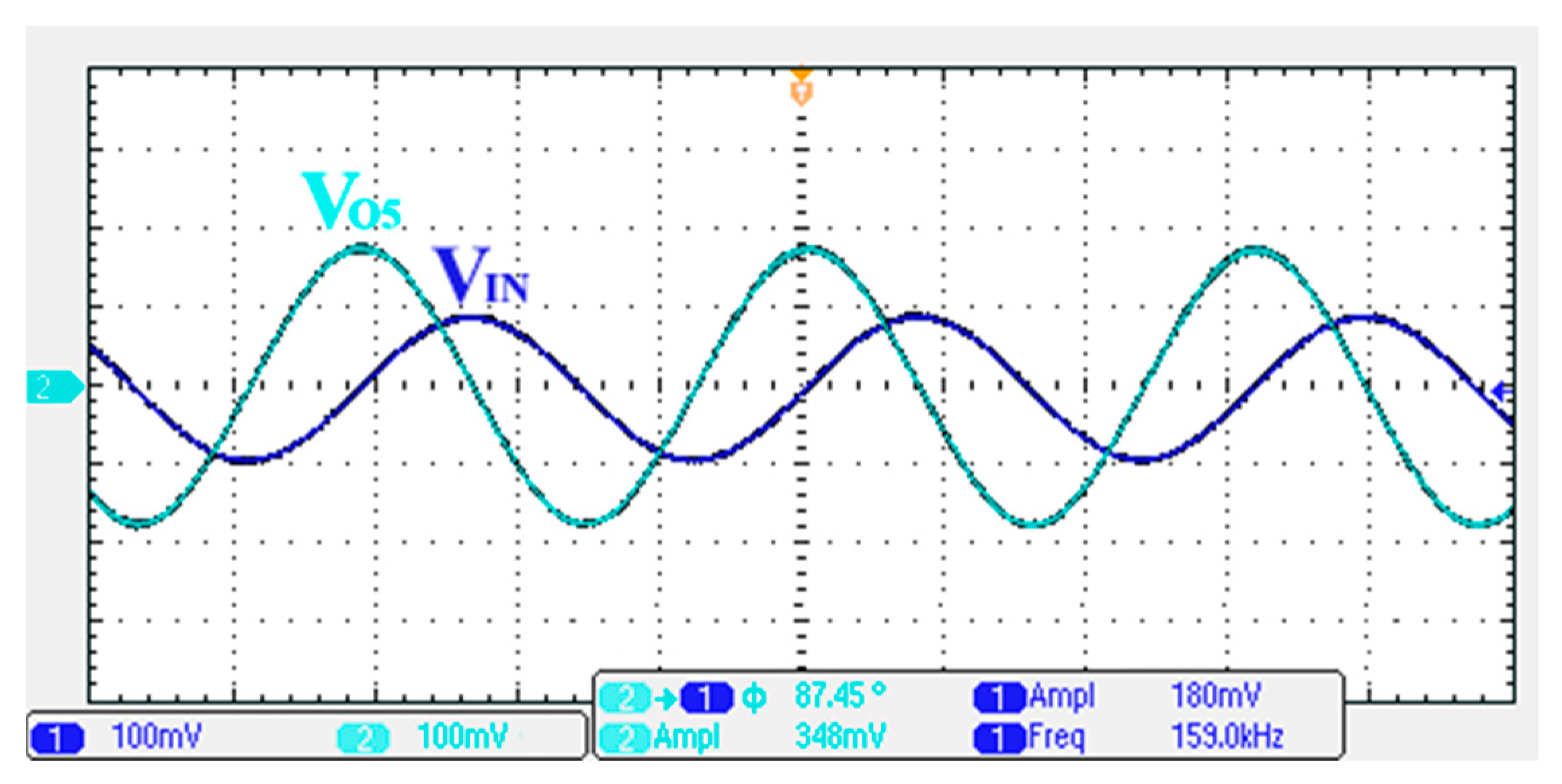
| Vo5 | 90° | 87.45° | −2.55° |
Table 7.
Summary of the measured performance of the second proposed VM LT1228-based second-order multifunction filter.
Table 7.
Summary of the measured performance of the second proposed VM LT1228-based second-order multifunction filter.
| Factor |
|---|
| Power Supply (V) | PD (W) | Pole Frequency (kHz) | Pole Frequency Tuning Range (kHz) | P1dB (dBm) | IMD3 (dBc) | TOI (dBm) | SFDR (dBc) |
|---|
| ±15 | 0.69 | 157.55 | 47.71–887.34 | −7 | −49.65 | 4.316 | 45.88 |


