

Anti-Blooming Clocking for Time-Delay Integration CCDs
 , ,
, ,
Abstract
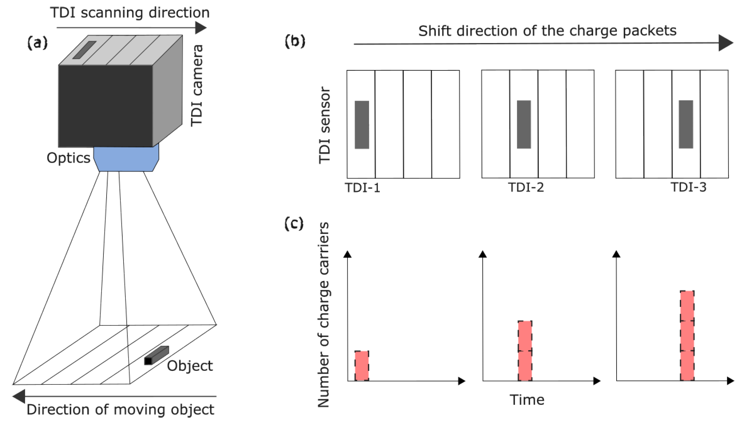
:1. Introduction
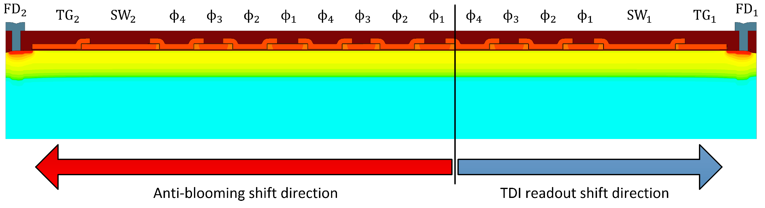
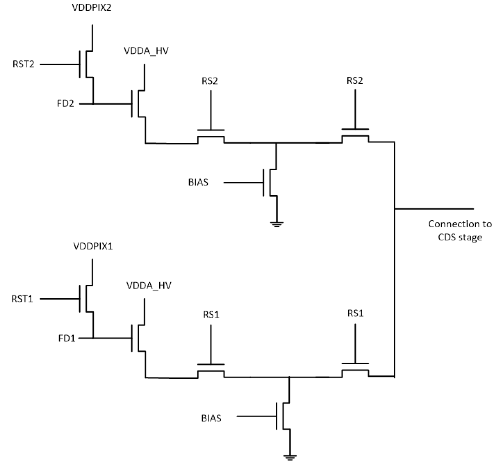
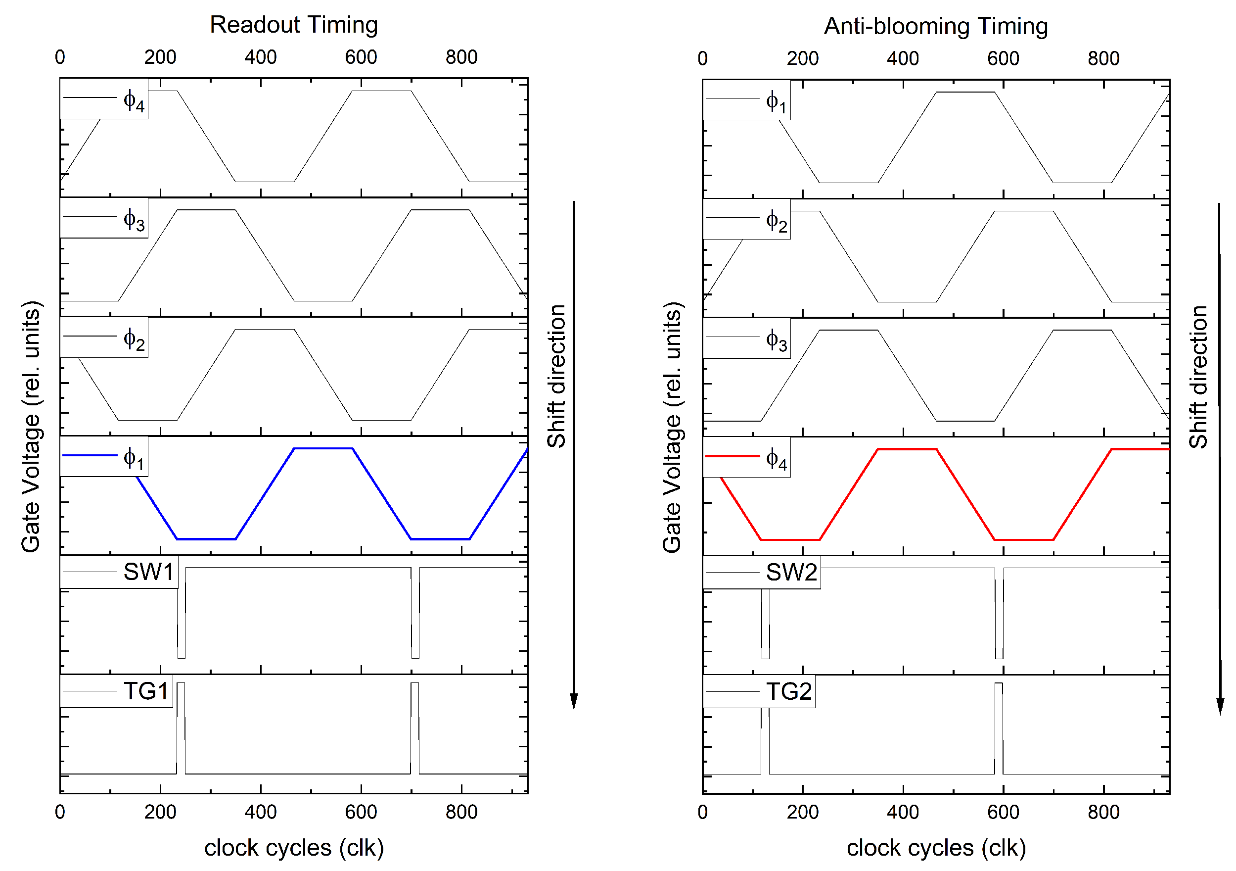
2. Design of the TDI CCD Chip
3. Experimental Results
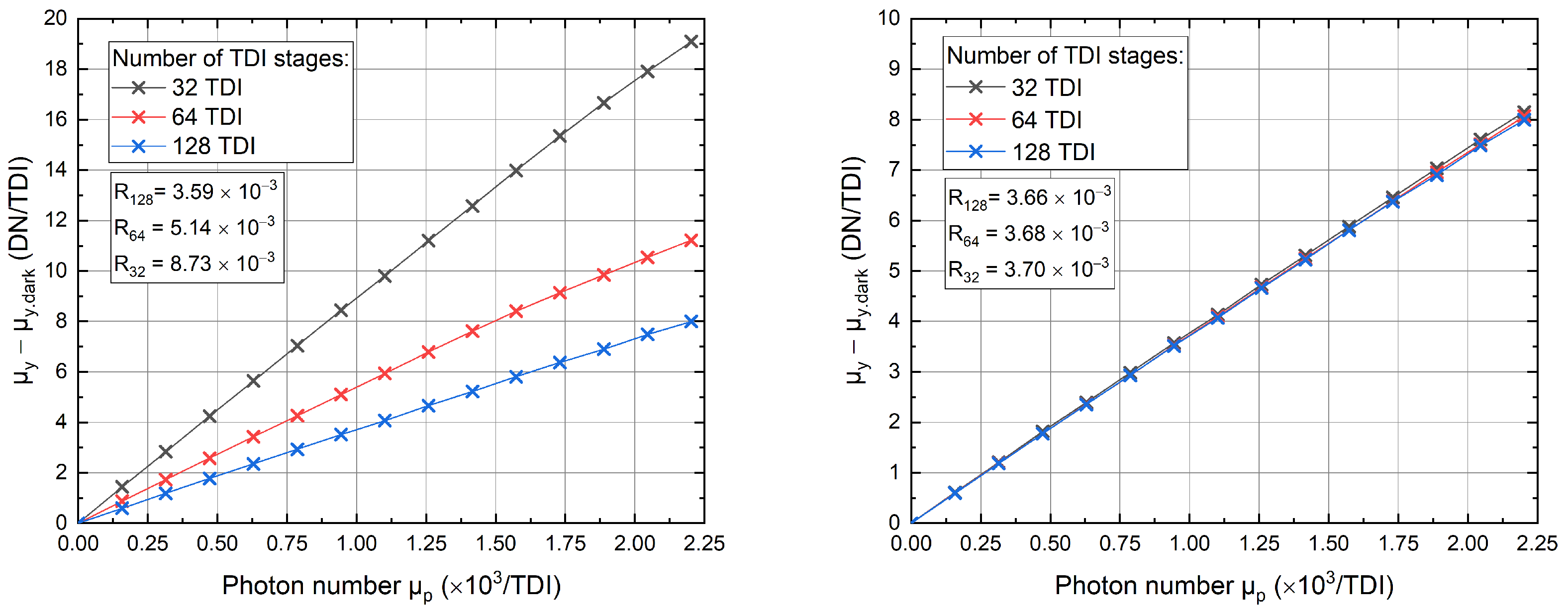
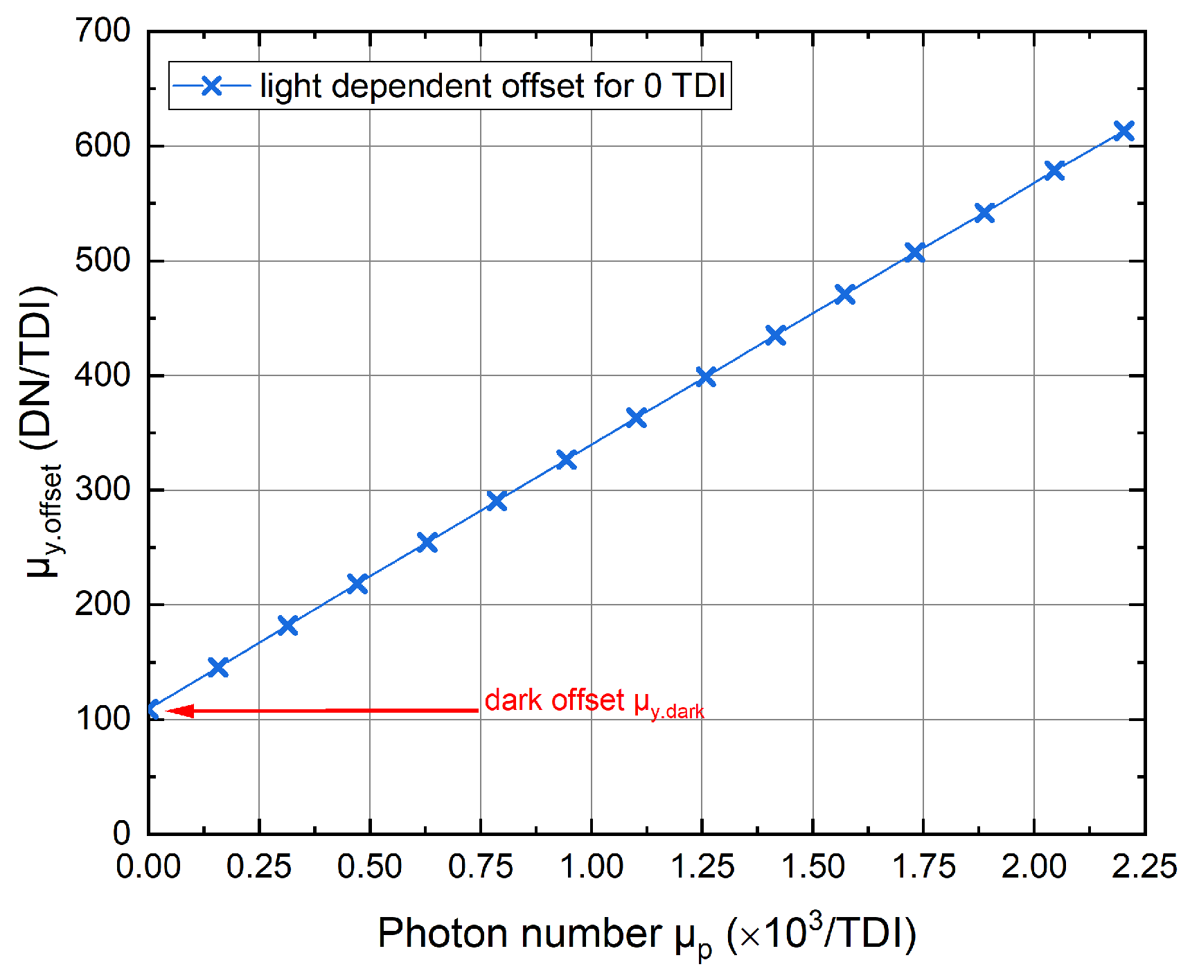
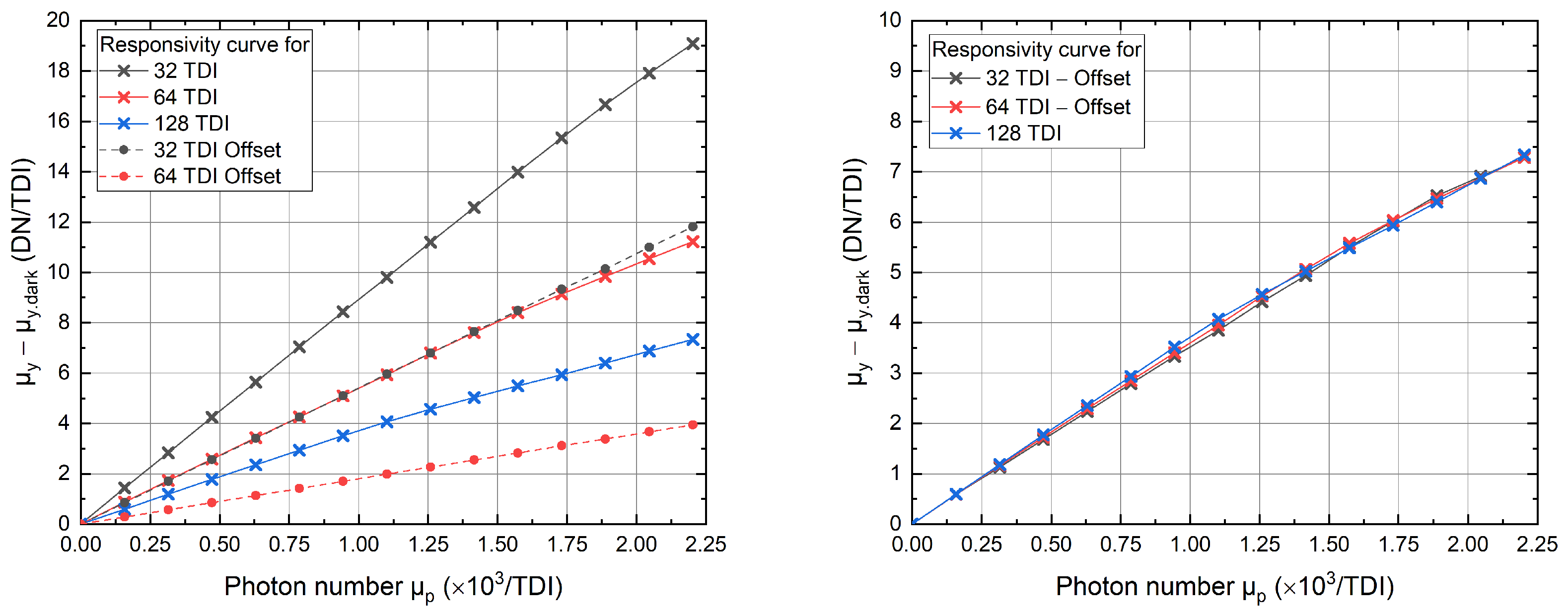
3.1. Responsivity
3.2. Photon Transfer Method and Signal-to-Noise Ratio
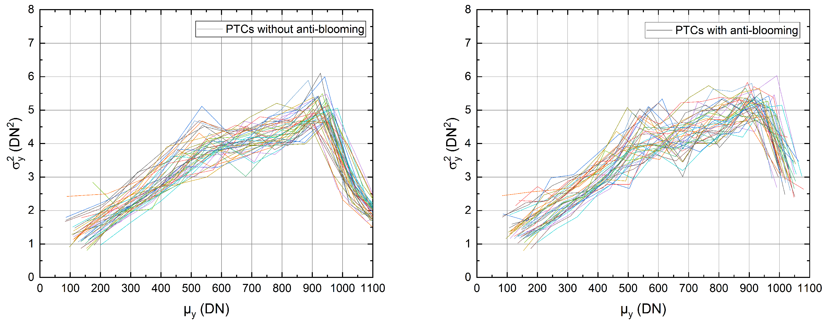
3.2.1. Photon Transfer Curve
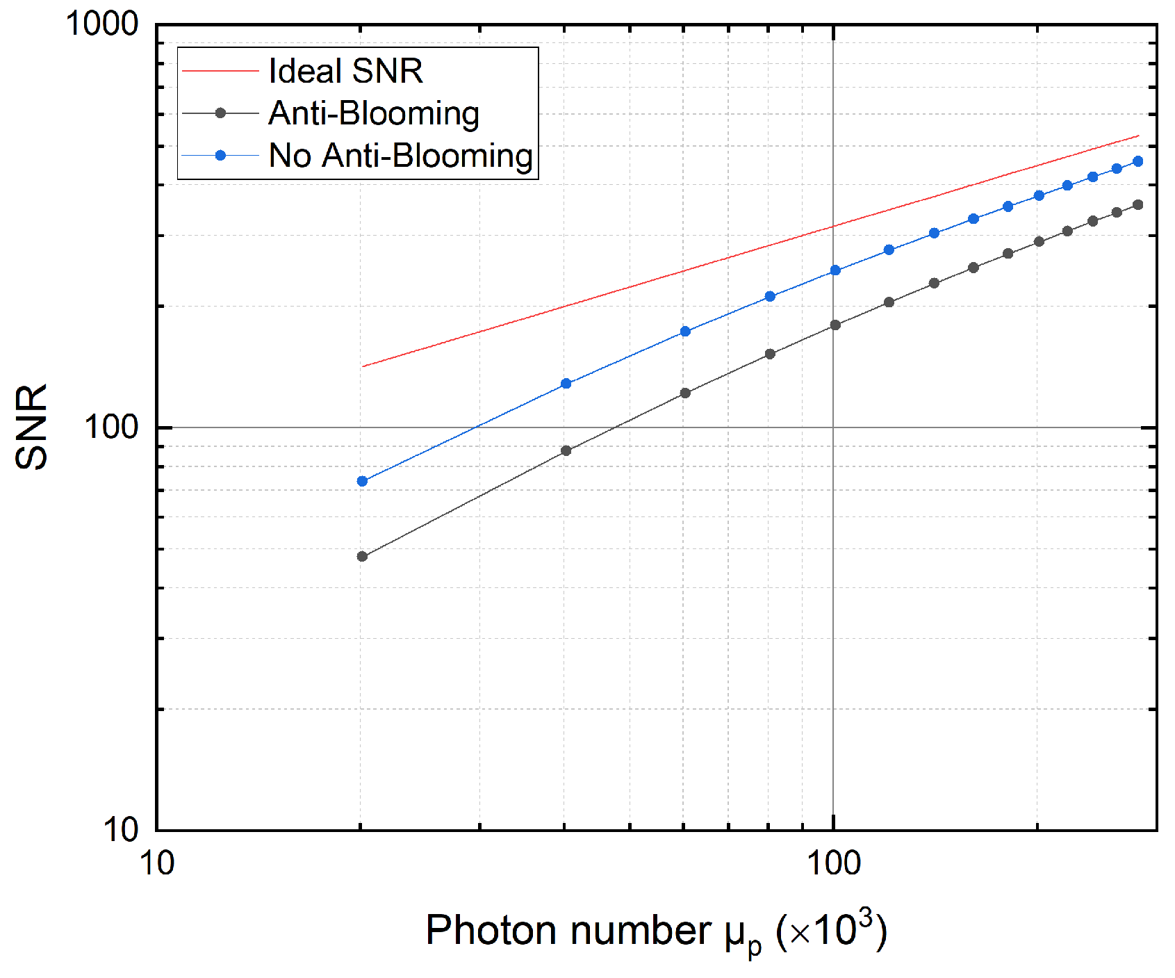
3.2.2. Signal-to-Noise Ratio
4. Discussion and Conclusions
Author Contributions
Funding
Institutional Review Board Statement
Informed Consent Statement
Data Availability Statement
Conflicts of Interest
References
- Rushton, J.E.; Stefanov, K.D.; Holland, A.D.; Endicott, J.; Mayer, F.; Barbier, F. A CMOS TDI image sensor for Earth observation. Nanophotonics and Macrophotonics for Space Environments IX. Proc. SPIE 2015, 9616, 217–227. [Google Scholar]
- Netten, H.; van Vliet, L.J.; Boddeke, F.R.; de Jong, P.; Young, I.T. A fast scanner for fluorescence microscopy using a 2-D CCD and time delayed integration. Bioimaging 1994, 2, 184–192. [Google Scholar] [CrossRef]
- Boulenc, P.; Robbelein, J.; Wu, L.; Haspeslagh, L.; De Moor, P.; Borremans, J.; Rosmeulen, M. High speed TDI embedded CCD in CMOS sensor. In Proceedings of the International Conference on Space Optics—ICSO 2016, Biarritz, France, 18–21 October 2016; Volume 10562, p. 105622P. [Google Scholar]
- Materne, A.; Bardoux, A.; Geoffray, H.; Tournier, T.; Kubik, P.; Morris, D.; Wallace, I.; Renard, C. Backthinned TDI CCD image sensor design and performance for the Pleiades high resolution earth observation satellites. In Proceedings of the International Conference on Space Optics—ICSO 2006, Noordwijk, The Netherlands, 27–30 June 2006; Volume 10567, p. 105671N. [Google Scholar]
- Kamasz, S.R.; Singh, S.P.; Ingram, S.G.; Kiik, M.J.; Tang, Q.; Benwell, B. Enhanced Full Well for Vertical Antiblooming, High Sensitivity Time-Delay and Integration (TDI) CCDs with GHz Data Rates. In Proceedings of the IEEE Workshop on Charge-Coupled Devices and Advanced Image Sensors, Lake Tahoe, NV, USA, 7–9 June 2001; Available online: https://www.imagesensors.org/Past%20Workshops/2001%20Workshop/2001%20Papers/pg%20209%20Kamasz.pdf (accessed on 27 September 2022).
- Farrier, M.; Dyck, R. A large area TDI image sensor for low light level imaging. IEEE J. Solid-State Circ. 1980, 15, 753–758. [Google Scholar] [CrossRef]
- Ercan, A.; Haspeslagh, L.; De Munck, K.; Minoglou, K.; Lauwers, A.; De Moor, P. Prototype TDI sensors in embedded CCD in CMOS technology. In Proceedings of the International Image Sensor Workshop, Snowbird, UT, USA, 12–16 June 2013. [Google Scholar]
- Eckardt, A.; Glaesener, S.; Reulke, R.; Sengebusch, K.; Zender, B. Status of the next generation CMOS-TDI detector for high-resolution imaging. Earth Obs. Syst. XXIV Int. Soc. Opt. Phot. 2019, 11127, 111270J. [Google Scholar]
- European Machine Vision Association. EMVA Standard 1288, standard for characterization of image sensors and cameras. Release 2010, 3, 29. [Google Scholar]
- Saks, N.S. Interface state trapping and dark current generation in buried-channel charge-coupled devices. J. Appl. Phys. 1982, 53, 1745–1753. [Google Scholar] [CrossRef]
- Ghannam, M.Y.; Kamal, H.A. Modeling surface recombination at the p-type Si/SiO2 interface via dangling bond amphoteric centers. Adv. Condens. Matter Phys. 2014, 2014, 857907. [Google Scholar] [CrossRef] [Green Version]
- Janesick, J.R. Photon Transfer; SPIE Press: Bellingham, WA, USA, 2007. [Google Scholar]
- Dierks, F. Sensitivity and Image Quality of Digital Cameras; Basler AG: Ahrensburg, Germany, 2004. [Google Scholar]
- Janesick, J.R.; Klaasen, K.P.; Elliott, T. Charge-coupled-device charge-collection efficiency and the photon-transfer technique. Opt. Eng. 1987, 26, 972–980. [Google Scholar] [CrossRef]
- Janesick, J.R. Scientific Charge-Coupled Devices; SPIE Press: Bellingham, WA, USA, 2001; Volume 83. [Google Scholar]


| Parameter | Anti-Blooming | No Anti-Blooming |
|---|---|---|
| Responsivity (DN) | ||
| Conversion Gain (DN/e) | ||
| Quantum Efficiency | 0.60 | 0.82 |
| SNR | 1–357 | 1–457 |
| Dynamic Range | 800 | 1270 |
Publisher’s Note: MDPI stays neutral with regard to jurisdictional claims in published maps and institutional affiliations. |
© 2022 by the authors. Licensee MDPI, Basel, Switzerland. This article is an open access article distributed under the terms and conditions of the Creative Commons Attribution (CC BY) license (https://creativecommons.org/licenses/by/4.0/).
Share and Cite
Piechaczek, D.S.; Schrey, O.; Ligges, M.; Hosticka, B.; Kokozinski, R. Anti-Blooming Clocking for Time-Delay Integration CCDs. Sensors 2022, 22, 7520. https://doi.org/10.3390/s22197520
Piechaczek DS, Schrey O, Ligges M, Hosticka B, Kokozinski R. Anti-Blooming Clocking for Time-Delay Integration CCDs. Sensors. 2022; 22(19):7520. https://doi.org/10.3390/s22197520
Chicago/Turabian StylePiechaczek, Denis Szymon, Olaf Schrey, Manuel Ligges, Bedrich Hosticka, and Rainer Kokozinski. 2022. "Anti-Blooming Clocking for Time-Delay Integration CCDs" Sensors 22, no. 19: 7520. https://doi.org/10.3390/s22197520