

Metasurfaces for Sensing Applications: Gas, Bio and Chemical
 and
and 
Abstract
:1. Introduction
2. Fundamentals of Metasurfaces
3. Application of Metasurfaces in Analyte Sensing
3.1. Bio Sensing
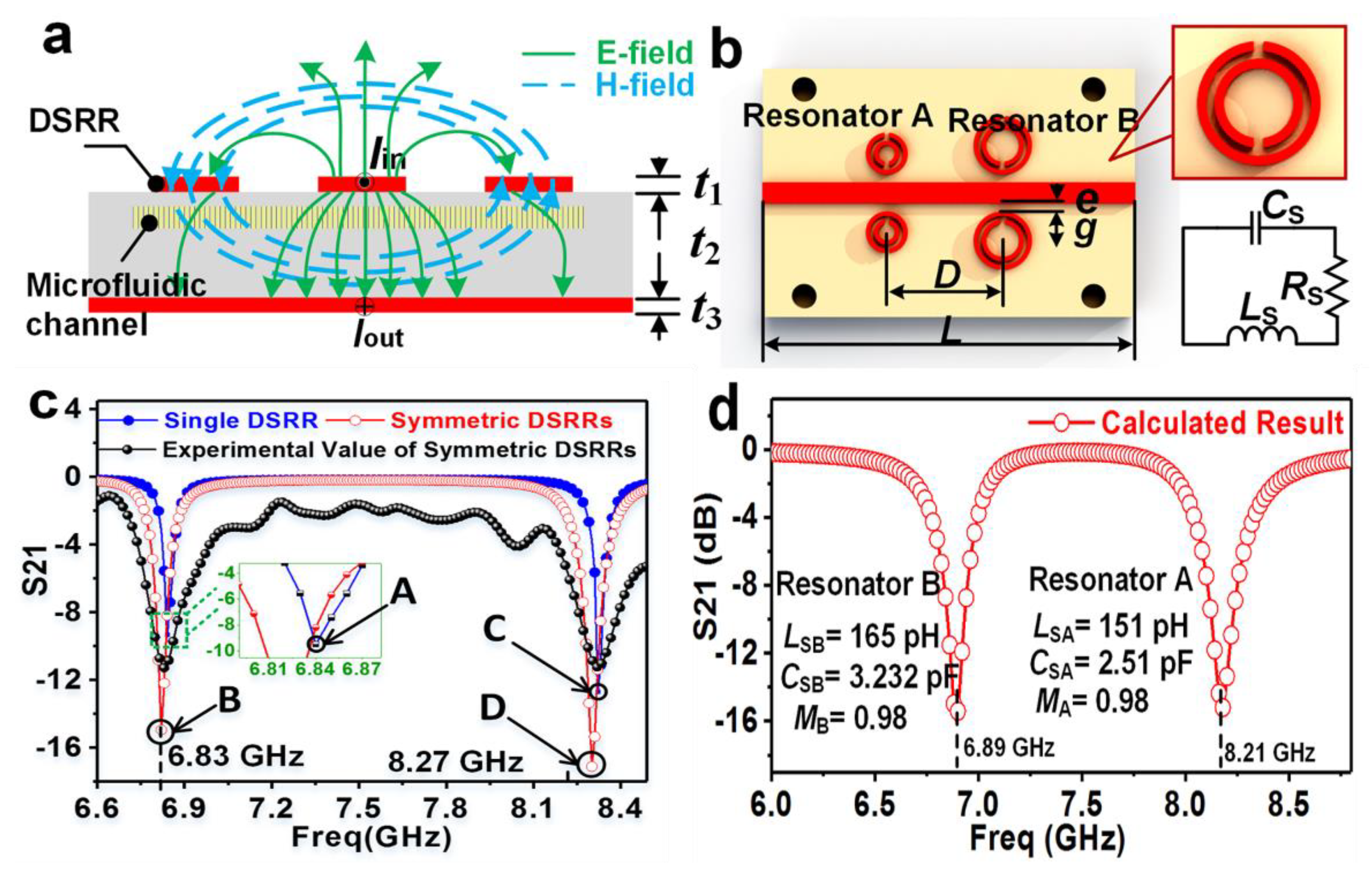
3.1.1. LC Resonator-Based Biosensors in THz/GHz Regime
3.1.2. Hyperbolic Metamaterials (HMMs)
3.2. Gas Sensing
3.2.1. Metamaterial Perfect Absorber/Emitter
3.2.2. Complementary Split-Ring Resonator
3.2.3. Metal-Insulator-Metal
3.3. Chemical Sensing
4. Future Trends in Metasurfaces for Sensing Applications
5. Conclusions
Author Contributions
Funding
Institutional Review Board Statement
Informed Consent Statement
Data Availability Statement
Conflicts of Interest
References
- Smith, D.R.; Pendry, J.B.; Wiltshire, M.C.K. Metamaterials and Negative Refractive Index. Science 2004, 305, 788–792. [Google Scholar] [CrossRef] [PubMed]
- Valentine, J.; Zhang, S.; Zentgraf, T.; Ulin-Avila, E.; Genov, D.A.; Bartal, G.; Zhang, X. Three-dimensional optical metamaterial with a negative refractive index. Nature 2008, 455, 376–379. [Google Scholar] [CrossRef] [PubMed]
- Hsu, L.; Ndao, A.; Kanté, B. Broadband and linear polarization metasurface carpet cloak in the visible. Opt. Lett. 2019, 44, 2978–2981. [Google Scholar] [CrossRef] [PubMed]
- Qian, C.; Zheng, B.; Shen, Y.C.; Jing, L.; Li, E.P.; Shen, L.; Chen, H.S. Deep-learning-enabled self-adaptive microwave cloak without human intervention. Nat. Photonics 2020, 14, 383–390. [Google Scholar] [CrossRef]
- Cheng, B.H.; Lan, Y.-C.; Tsai, D.P. Breaking optical diffraction limitation using optical Hybrid-Super-Hyperlens with radially polarized light. Opt. Express 2013, 21, 14898–14906. [Google Scholar] [CrossRef] [PubMed]
- Azad, S.; Mishra, S.K.; Rezaei, G.; Izquierdo, G.; Ung, B. Rapid and sensitive magnetic field sensor based on photonic crystal fiber with magnetic fluid infiltrated nanoholes. Sci. Rep. 2022, 12, 9676. [Google Scholar] [CrossRef]
- Mishra, S.K.; Mishra, A.K.; Misra, K.P.; Verma, R.K. Detection of alcohol content in food products by lossy mode resonance technique. J. Electrochem. Society 2022, 15, 32–38. [Google Scholar]
- Mishra, S.K.; Thiong, J.-M.-M.; Wagnac, E.; Petit, Y.; Ung, B. A sensitive and fast Bragg grating-based investigations of the biochemical dynamics of in vitro spinal cord injuries. Sensors 2021, 22, 1671. [Google Scholar] [CrossRef]
- Pathak, A.; Mishra, S.K.; Gupta, B.D. Fiber-optic ammonia sensor using Ag/SnO2 thin films: Optimization of thickness of SnO2 film using electric field distribution and reaction factor. Appl. Opt. 2011, 54, 8712–8721. [Google Scholar] [CrossRef]
- Azad, S.; Khosravi, M.; Nikzad, A.; Mishra, S.K. A novel contemporary molecular imprinting techniques for nan enzymatic selective glucose detection. Opt. Laser Technol. 2022, 148, 107786. [Google Scholar] [CrossRef]
- Shrivastav, A.M.; Mishra, S.K.; Gupta, B. Localized and propagating surface plasmon resonance-based fiber optic sensor for the detection of tetracycline using molecular imprinting. Mater. Res. Express 2015, 2, 035007. [Google Scholar] [CrossRef]
- Mishra, S.K.; Verma, R.K.; Mishra, A.K. Versatile sensing structure: GaP/Au/Graphene/Silicone. Photonics 2021, 8, 547. [Google Scholar] [CrossRef]
- Zhang, X.; Liu, Z. Superlenses to overcome the diffraction limit. Nat. Mater. 2008, 7, 435–441. [Google Scholar] [CrossRef] [PubMed]
- Cheng, B.H.; Ho, Y.Z.; Lan, Y.-C.; Tsai, D.P. Optical Hybrid-Superlens Hyperlens for Superresolution Imaging. IEEE J. Sel. Top. Quantum Electron. 2013, 19, 4601305. [Google Scholar] [CrossRef]
- Murray, W.A.; Barnes, W.L. Plasmonic materials. Adv. Mater. 2007, 19, 3771–3782. [Google Scholar] [CrossRef]
- Larouche, S.; Tsai, Y.-J.; Tyler, T.; Jokerst, N.M.; Smith, D.R. Infrared metamaterial phase holograms. Nat. Mater. 2012, 11, 450–454. [Google Scholar] [CrossRef] [PubMed]
- Güney, D.O.; Koschny, T.; Soukoulis, C.M. Reducing ohmic losses in metamaterials by geometric tailoring. Phys. Rev. B 2009, 80, 125129. [Google Scholar] [CrossRef]
- Liu, N.; Guo, H.C.; Fu, L.W.; Kaiser, S.; Schweizer, H.; Giessen, H. Three-dimensional photonic metamaterials at optical frequencies. Nat. Mater. 2008, 7, 31–37. [Google Scholar] [CrossRef]
- Wu, P.C.; Liao, C.Y.; Chen, J.-W.; Tsai, D.P. Isotropic Absorption and Sensor of Vertical Split-Ring Resonator. Adv. Opt. Mater. 2017, 5, 1600581. [Google Scholar] [CrossRef]
- Holloway, C.; Dienstfrey, A.; Kuester, E.F.; O’Hara, J.F.; Azad, A.K.; Taylor, A.J. A discussion on the interpretation and characterization of metafilms/metasurfaces: The two-dimensional equivalent of metamaterials. Metamaterials 2009, 3, 100–112. [Google Scholar] [CrossRef]
- Holloway, C.; Kuester, E.F.; Gordon, J.; O’Hara, J.; Booth, J.; Smith, D. An overview of the theory and applications of metasurfaces: The two-dimensional equivalents of metamaterials. IEEE Antennas Propag. Mag. 2012, 54, 10–35. [Google Scholar] [CrossRef]
- Minovich, A.E.; Miroshnichenko, A.E.; Bykov, A.Y.; Murzina, T.V.; Neshev, D.N.; Kivshar, Y.S. Functional and nonlinear optical metasurfaces. Laser Photon Rev. 2015, 9, 195–213. [Google Scholar] [CrossRef]
- Glybovski, S.B.; Tretyakov, S.A.; Belov, P.A.; Kivshar, Y.S.; Simovski, C.R. Metasurfaces: From microwaves to visible. Phys. Rep. 2016, 634, 1–72. [Google Scholar] [CrossRef]
- Kildishev, A.V.; Boltasseva, A.; Shalaev, V.M. Planar photonics with metasurfaces. Science 2013, 339, 1232009. [Google Scholar] [CrossRef] [PubMed]
- Lamb, H. On the reflection and transmission of electric waves by a metallic grating. Proc. Lond. Math. Soc. 1897, 1, 523–546. [Google Scholar] [CrossRef]
- Marconi, G.; Franklin, C. Reflector for Use in Wireless Telegraphy and Telephony. U.S. Patent 1,301,473, 22 April 1919. [Google Scholar]
- Buskirk, L.V.; Hendrix, C. The zone plate as a radio-frequency focusing element. IRE Trans. Antennas Propag. 1961, 9, 319–320. [Google Scholar] [CrossRef]
- Veselago, V.G. The electrodynamics of substances with simultaneously negative values of ε, and μ. Sov. Phys. Usp. 1968, 47, 509–514. [Google Scholar] [CrossRef]
- Pendry, J.B.; Holden, A.J.; Robbins, D.J.; Stewart, W.J. Low Frequency Plasmons for Thin-Wire Structure. J. Phys. Condens. Matter 1998, 10, 4785–4809. [Google Scholar] [CrossRef]
- Pendry, J.B.; Holden, A.J.; Robins, D.J.; Stewart, W.J. Magnetism from conductors and enhanced non-linear phenomena. IEEE Trans. Microw. Theory Tech. 1999, 47, 2075–2084. [Google Scholar] [CrossRef]
- Smith, D.R.; Padila, W.J.; Vier, D.C.; Nemat-Naseer, S.C.; Schultz, S. Composite medium with simultaneously Negative permeability and permittivity. Phys. Rev. Lett. 2000, 84, 4184–4187. [Google Scholar] [CrossRef]
- Lee, Y.; Kim, S.J.; Park, H.; Lee, B. Metamaterials and Metasurfaces for sensor applications. Sensors 2017, 17, 1726. [Google Scholar] [CrossRef] [PubMed] [Green Version]
- Karawdeniya, B.I.; Damry, A.M.; Murugappan, K.; Manjunath, S.; Nuwan, Y.M. Surface functionalization and texturing of optical Metasurfaces for sensing applications. Chem. Rev. 2022, 107, 2411–2502. [Google Scholar] [CrossRef] [PubMed]
- Decker, M.; Staude, I.; Falkner, M.; Dominguez, J.; Neshev, D.N.; Brener, I.; Pertsch, T.; Kivshar, Y.S. High-efficiency dielectric Huygens’ surfaces. Adv. Opt. Mater. 2015, 3, 813–820. [Google Scholar] [CrossRef]
- Modi, K.S.; Kaur, J.; Singh, S.P.; Sinha, R.K. Extremely high figure of merit in all-dielectric split asymmetric arc Metasurface for refractive index sensing. Opt. Commun. 2020, 462, 125327. [Google Scholar] [CrossRef]
- Zhang, J.; Liu, W.; Zhu, Z.; Yuan, X.; Qin, S. Strong field enhancement and light matter interactions with all-dielectric metamaterials based on split bar resonator. Opt. Express 2014, 22, 30889–30898. [Google Scholar] [CrossRef]
- Alipour, A.; Farmani, A.; Mir, A. High sensitivity and tunable nanoscale sensor based on plasmon-induced transparency in plasmonic metasurface. IEEE Sens. J. 2018, 18, 7047–7054. [Google Scholar] [CrossRef]
- Komar, A.; Fang, Z.; Bohn, J.; Sautter, J.; Decker, M.; Miroshnichenko, A.; Pertsch, T.; Brener, I.; Kivshar, Y.S.; Stude, I. Electrically tunable all-dielectric optical metasurfaces based on liquid crystal. Appl. Phys. 2017, 110, 071109. [Google Scholar] [CrossRef]
- Su, H.; Wang, H.; Zhao, H.; Xue, T.; Zhang, J. Liquid-crystal based electrically tuned electromagnetically induced transparency metasurface switch. Sci. Rep. 2017, 7, 17378. [Google Scholar] [CrossRef]
- Chen, H.T.; Taylor, A.J.; Yu, N. A review of metasurfaces: Physics and applications. Rep. Prog. Phys. 2016, 79, 076401. [Google Scholar] [CrossRef]
- Liu, T.; Wang, H.; Liu, Y.; Xiao, L.; Yi, Z.; Zhou, C.; Xiao, S. Active manipulation of electromagnetically induced transparency in a terahertz hybrid metamaterial. Opt. Commun. 2018, 426, 629–634. [Google Scholar] [CrossRef]
- Smith, D.; Vier, D.; Koschny, T.; Soukoulis, C. Electromagnetic parameter retrieval from inhomogeneous metamaterials. Phys. Rev. E 2005, 71, 036617. [Google Scholar] [CrossRef] [PubMed] [Green Version]
- Cai, W.; Shalaev, V. Optical Metamaterials: Fundamentals and Applications, 1st ed.; Springer: New York, NY, USA, 2010; pp. 1–8. [Google Scholar]
- Luk’yanchuk, B.; Zheludev, N.I.; Maier, S.A.; Halas, N.J.; Nordlander, P.; Giessen, H.; Chong, C.T. The Fano resonance in plasmonic nanostructures and metamaterials. Nat. Mat. 2010, 9, 707–715. [Google Scholar] [CrossRef]
- Jorgenson, R.C.; Yee, S.S. A fiber-optic chemical sensor based on surface plasmon resonance. Sens. Actuators B Chem. 1993, 12, 213–220. [Google Scholar] [CrossRef]
- Shankaran, D.R.; Gobi, K.V.; Miura, N. Recent advancements in surface plasmon resonance immunosensors for detection of small molecules of biomedical, food and environmental interest. Sens. Actuators B Chem. 2007, 121, 158–177. [Google Scholar] [CrossRef]
- Kretschmann, E.; Raether, H. Radiative decay of non-radiative surface plasmons excited by light. Nature 1968, 23, 2135–2136. [Google Scholar] [CrossRef]
- Helmerhorst, E.; Chandler, D.J.; Nussio, M.; Mamotte, C.D. Real-time and label-free bio-sensing of molecular interactions by surface plasmon resonance: A laboratory medicine perspective. Clin. Biochem. Rev. 2012, 33, 161–173. [Google Scholar]
- Lin, Z.; Xu, Z.; Liang, Z.; Lin, Y.S. Polarization-sensitive terahertz resonator using asymmetrical F-shaped metamaterial. Opt. Laser Technol. 2020, 121, 105826. [Google Scholar] [CrossRef]
- Hong, J.T.; Jun, S.W.; Cha, S.H.; Park, J.Y.; Lee, S.; Shin, G.A.; Ahn, Y.H. Enhanced sensitivity in THz plasmonic sensors with silver nanowires. Sci. Rep. 2018, 8, 15536. [Google Scholar] [CrossRef]
- Wang, X.; Li, Y.; Wang, H.; Fu, Q.; Peng, J.; Wang, Y.; Du, J.; Zhou, Y.; Zhan, L. Gold nanorod-based localized surface plasmon resonance biosensor for sensitive detection of hepatitis B virus in buffer, blood serum and plasma. Biosens. Bioelectron. 2010, 26, 404–410. [Google Scholar] [CrossRef]
- Ahmadivand, A.; Gerislioglu, B.; Tomitaka, A.; Manickam, P.; Kaushik, A.; Bhansali, S.; Nair, M.; Pala, N. Extreme sensitive metasensor for targeted biomarkers identification using colloidal nanoparticles-integrated plasmonic unit cells. Biomed. Opt. Express 2018, 9, 373–386. [Google Scholar] [CrossRef]
- Diao, W.; Tang, M.; Ding, S.; Li, X.; Cheng, W.; Mo, F.; Yan, X.; Ma, H.; Yan, Y. Highly sensitive surface plasmon resonance biosensor for the detection of HIV-related DNA based on dynamic and structural DNA nanodevices. Biosens. Bioelectron. 2018, 100, 228–234. [Google Scholar] [CrossRef] [PubMed]
- Lee, S.H.; Lee, Y.K.; Lee, S.H.; Kwak, J.; Song, H.S.; Seo, M. Detection and discrimination of SARS-CoV-2 spike protein-derived peptides using THz metamaterials. Biosens. Bioelectron. 2022, 202, 113981. [Google Scholar] [CrossRef] [PubMed]
- Minopoli, A.; Della Ventura, B.; Lenyk, B.; Gentile, F.; Tanner, J.A.; Offenhäusser, A.; Mayer, D.; Velotta, R. Ultrasensitive antibody-aptamer plasmonic biosensor for malaria biomarker detection in whole blood. Nat. Commun. 2020, 11, 6134. [Google Scholar] [CrossRef]
- Lee, H.J.; Yook, J.G. Biosensing using split-ring resonators at microwave regime. Appl. Phys. Lett. 2008, 92, 254103. [Google Scholar] [CrossRef]
- Kashiwagi, K.; Xie, L.; Li, X.; Kageyama, T.; Miura, M.; Miyashita, H.; Kono, J.; Lee, S.-S. Flexible and stackable terahertz metamaterials via silver-nanoparticle inkjet printing. AIP Adv. 2018, 8, 045104. [Google Scholar] [CrossRef]
- Tao, H.; Chieffo, L.R.; Brenckle, M.A.; Siebert, S.M.; Liu, M.; Strikwerda, A.C.; Fan, K.; Kaplan, D.L.; Zhang, X.; Averitt, R.D.; et al. Metamaterials on paper as a sensing platform. Adv. Mater. 2011, 23, 3197–3201. [Google Scholar] [CrossRef]
- Park, S.J.; Cha, S.H.; Shin, G.A.; Ahn, Y.H. Sensing viruses using terahertz nano-gap metamaterials. Biomed. Opt. Express 2017, 8, 3551–3558. [Google Scholar] [CrossRef]
- Park, S.J.; Hong, J.T.; Choi, S.J.; Kim, H.S.; Park, W.K.; Han, S.T.; Park, J.Y.; Lee, S.; Kim, D.S.; Ahn, Y.H. Detection of microorganisms using terahertz metamaterials. Sci. Rep. 2014, 4, 4988. [Google Scholar] [CrossRef]
- Marsland, B.J.; Gollwitzer, E.S. Host–microorganism interactions in lung diseases. Nat. Rev. Immunol. 2014, 14, 827–835. [Google Scholar] [CrossRef]
- Kim, K.S. Pathogenesis of bacterial meningitis: From bacteraemia to neuronal injury. Nat. Rev. Neurosci. 2003, 4, 376–385. [Google Scholar] [CrossRef]
- Chen, H.T.; Padilla, W.J.; Zide, J.M.O.; Gossard, A.C.; Taylor, A.J.; Averitt, R.D. Active terahertz metamaterial devices. Nature 2006, 444, 597–600. [Google Scholar] [CrossRef] [PubMed]
- Li, Y.; Chen, X.; Hu, F.; Li, D.; Teng, H.; Rong, Q.; Zhang, W.; Han, J.; Liang, H. Four resonators based high sensitive terahertz metamaterial biosensor used for measuring concentration of protein. J. Phys. D Appl. Phys. 2019, 52, 095105. [Google Scholar] [CrossRef]
- Liu, K.; Zhang, R.; Liu, Y.; Chen, X.; Li, K.; Pickwell-Macpherson, E. Gold nanoparticle enhanced detection of EGFR with a terahertz metamaterial biosensor. Biomed. Opt. Express 2021, 12, 1559–1567. [Google Scholar] [CrossRef] [PubMed]
- Bossi, P.; Resteghini, C.; Paielli, N.; Licitra, L.; Pilotti, S.; Perrone, F. Prognostic and predictive value of EGFR in head and neck squamous cell carcinoma. Oncotarget 2016, 7, 74362–74379. [Google Scholar] [CrossRef] [PubMed]
- Lee, C.K.; Man, J.; Lord, S.; Links, M.; Gebski, V.; Mok, T.; Yang, J.C. Checkpoint inhibitors in metastatic EGFR-mutated non–small cell lung cancer—a meta-analysis. J. Thorac. Oncol. 2017, 12, 403–407. [Google Scholar] [CrossRef]
- Tao, H.; Strikwerda, A.C.; Liu, M.; Mondia, J.P.; Ekmekci, E.; Fan, K.; Kaplan, D.L.; Padilla, W.J.; Zhang, X.; Averitt, R.D.; et al. Performance enhancement of terahertz metamaterials on ultrathin substrates for sensing applications. Appl. Phys. Lett. 2010, 97, 261909. [Google Scholar] [CrossRef]
- Yang, Y.; Singh, R.; Zhang, W. Anomalous terahertz transmission in bow-tie plasmonic antenna apertures. Opt. Lett. 2011, 36, 2901–2903. [Google Scholar] [CrossRef]
- Novelli, F.; Guchhait, B.; Havenith, M. Towards intense THz spectroscopy on water: Characterization of optical rectification by GaP, OH1, and DSTMS at OPA Wavelengths. Materials 2020, 13, 1311. [Google Scholar] [CrossRef]
- Geng, Z.; Zhang, X.; Fan, Z.; Lv, X.; Chen, H. A route to terahertz metamaterial biosensor integrated with microfluidics for liver cancer biomarker testing in early stage. Sci. Rep. 2017, 7, 16378. [Google Scholar] [CrossRef]
- Chen, H.; Kou, X.; Yang, Z.; Ni, W.; Wang, J. Shape- and size-dependent refractive index sensitivity of gold nanoparticles. Langmuir 2008, 24, 5233–5237. [Google Scholar] [CrossRef]
- Sannomiya, T.; Vörös, J. Single plasmonic nanoparticles for biosensing. Trends Biotechnol. 2011, 29, 343–351. [Google Scholar] [CrossRef] [PubMed]
- Kabashin, A.V.; Evans, P.; Pastkovsky, S.; Hendren, W.; Wurtz, G.A.; Atkinson, R.; Pollard, R.; Podolskiy, V.A.; Zayats, A.V. Plasmonic nanorod metamaterials for biosensing. Nat. Mater. 2009, 8, 867–871. [Google Scholar] [CrossRef] [PubMed]
- Sreekanth, K.V.; Alapan, Y.; ElKabbash, M.; Ilker, E.; Hinczewski, M.; Gurkan, U.A.; De Luca, A.; Strangi, G. Extreme sensitivity biosensing platform based on hyperbolic metamaterials. Nat. Mater. 2016, 15, 621–627. [Google Scholar] [CrossRef]
- Ihokura, K. The effects of crystallite size of sintered tin-dioxide on changes of electric conductivity in deoxidizable gases. J. Electrochem. Soc. Jpn. 1982, 50, 99–104. [Google Scholar]
- Saji, K.; Kondo, H.; Takahashi, H.; Takeuchi, T.; Igarashi, I. Influence of H2O, CO2 and various combustible gases on the characteristics of a limiting current-type oxygen sensor. J. Appl. Electrochem. 1988, 18, 757–762. [Google Scholar] [CrossRef]
- Nitta, T.; Terada, Z.; Hayakawa, S. Humidity-sensitive electrical conduction of MgCr2O4-TiO2 porous ceramics. J. Am. Ceram. Soc. 1980, 63, 295–300. [Google Scholar] [CrossRef]
- Bunte, G.; Hürttlen, J.; Pontius, H.; Hartlieb, K.; Krause, H. Gas phase detection of explosives Such as 2,4,6-trinitrotoluene by molecularly imprinted polymers. Anal. Chim. Acta 2007, 591, 49–56. [Google Scholar] [CrossRef]
- Kehe, K.; Szinicz, L. Medical aspects of sulphur mustard poisoning. Toxicology 2005, 214, 198–209. [Google Scholar] [CrossRef]
- Blumenthal, I. Carbon Monoxide Poisoning. J. R. Soc. Med. 2001, 94, 270–272. [Google Scholar] [CrossRef]
- Kumar, R.; Jaiswal, M.; Kushwaha, N.; Bansal, S.; Mazumder, N.; Mittal, J. Nanomaterial-based gas sensors for agriculture sector. In Biosensors in Agriculture: Recent Trends and Future Perspectives—Concepts and Strategies in Plant Sciences; Pudake, R.N., Jain, U., Kole, C., Eds.; Springer: Cham, Switzerland, 2021. [Google Scholar] [CrossRef]
- Nazemi, H.; Joseph, A.; Park, J.; Emadi, A. Advanced micro- and nano-gas sensor technology: A review. Sensors 2019, 19, 1285. [Google Scholar] [CrossRef]
- Mishra, S.K.; Gupta, B.D. Surface plasmon resonance-based fiber optic chlorine gas sensor utilizing indium-oxide-doped tin oxide film. J. Lightwave Technol. 2015, 33, 2770–2776. [Google Scholar] [CrossRef]
- Liu, J.; Zhang, L.; Fan, J.; Yu, J. Semiconductor gas sensor for triethylamine detection. Small 2022, 18, 2104984. [Google Scholar] [CrossRef] [PubMed]
- Zhu, H.; Li, Q.; Ren, Y.; Gao, Q.; Chen, J.; Wang, N.; Deng, J.; Xing, X. A new insight into cross-sensitivity to humidity of SnO2 sensor. Small 2018, 14, 1703974. [Google Scholar] [CrossRef] [PubMed]
- Zhang, Y.; Yi, Z.; Wang, X.; Chu, P.; Yao, W.; Zhou, Z.; Cheng, S.; Liu, Z.; Wu, P.; Pan, M.; et al. Dual band visible metamaterial absorbers based on four identical ring patches. Phys. E Low-Dimens. Syst. Nanostructures 2021, 127, 114526. [Google Scholar] [CrossRef]
- Park, J.-H.; Kodigala, A.; Ndao, A.; Kanté, B. Hybridized metamaterial platform for nano-scale sensing. Opt. Express 2017, 25, 15590–15598. [Google Scholar] [CrossRef]
- Jeong, T.-Y.; Gu, J.-H.; Choi, W.-Y.; No, Y.-S. Characteristics of a vertical metal-insulator-metal microring cavity. J. Korean Phys. Soc. 2018, 73, 580–585. [Google Scholar] [CrossRef]
- Su, D.-S.; Tsai, D.P.; Yen, T.-J.; Tanaka, T. Ultrasensitive and selective gas sensor based on a channel plasmonic structure with an enormous hot spot region. ACS Sens. 2019, 4, 2900–2907. [Google Scholar] [CrossRef]
- Bozhevolnyi, S.I. Effective-index modeling of channel plasmon polaritons. Opt. Express 2006, 14, 9467–9476. [Google Scholar] [CrossRef]
- Occupational Safety and Health Guideline for n-Butane; U.S. Department of Health and Human Services: Washington, DC, USA, 1992; pp. 1–5.
- Lochbaum, A.; Dorodnyy, A.; Koch, U.; Koepfli, S.M.; Volk, S.; Fedoryshyn, Y.; Wood, V.; Leuthold, J. Compact mid-infrared gas sensing enabled by an all-metamaterial design. Nano Lett. 2020, 20, 4169–4176. [Google Scholar] [CrossRef]
- Lashof, D.A.; Ahuja, D.R. Relative contributions of greenhouse gas emissions to global warming. Nature 1990, 344, 529–531. [Google Scholar] [CrossRef]
- Anderson, T.R.; Hawkins, E.; Jones, P.D. CO2 the greenhouse effect and global warming: From the pioneering work of Arrhenius and Callendar to today’s earth system models. Endeavour 2016, 40, 178–187. [Google Scholar] [CrossRef] [PubMed]
- Hansen, J.; Sato, M.; Kharecha, P.; Beerling, D.; Berner, R.; Masson-Delmotte, V.; Pagani, M.; Raymo, M.; Royer, D.L.; Zachos, J.C. Target atmospheric CO2: Where should humanity aim? Open Atmos. Sci. J. 2008, 2, 217–231. [Google Scholar] [CrossRef] [Green Version]
- Kazanskiy, N.L.; Butt, M.A.; Khonina, S.N. Carbon dioxide gas sensor based on polyhexamethylene biguanide polymer deposited on silicon nano-cylinders metasurface. Sensors 2021, 21, 378. [Google Scholar] [CrossRef]
- Lochbaum, A.; Fedoryshyn, Y.; Dorodnyy, A.; Koch, U.; Hafner, C.; Leuthold, J. On-chip narrowband thermal emitter for mid-IR optical gas sensing. ACS Photonics 2017, 4, 1371–1380. [Google Scholar] [CrossRef]
- Pusch, A.; De Luca, A.; Oh, S.S.; Wuestner, S.; Roschuk, T.; Chen, Y.; Boual, S.; Ali, Z.; Phillips, C.C.; Hong, M.; et al. A highly efficient CMOS nanoplasmonic crystal enhanced slow-wave thermal emitter improves infrared gas-sensing devices. Sci. Rep. 2015, 5, 17451. [Google Scholar] [CrossRef] [PubMed]
- Hasan, D.; Lee, C. Hybrid metamaterial absorber platform for sensing of CO2 gas at mid-IR. Adv. Sci. 2018, 5, 1700581. [Google Scholar] [CrossRef]
- Oertel, C.; Matschullat, J.; Zurba, K.; Zimmermann, F.; Erasmi, S. Greenhouse gas emissions from soils—A review. Geochemistry 2016, 76, 327–352. [Google Scholar] [CrossRef]
- Schliesser, A.; Picqué, N.; Hänsch, T.W. Mid-infrared frequency combs. Nat. Photonics 2012, 6, 440–449. [Google Scholar] [CrossRef]
- Tan, X.; Zhang, H.; Li, J.; Wan, H.; Guo, Q.; Zhu, H.; Liu, H.; Yi, F. Non-dispersive infrared multi-gas sensing via nanoantenna integrated narrowband detectors. Nat. Commun. 2020, 11, 5245. [Google Scholar] [CrossRef]
- Restrepo, C.E. Nitrogen dioxide, greenhouse gas emissions and transportation in urban areas: Lessons from the COVID-19 pandemic. Front. Environ. Sci. 2021, 9, 689985. [Google Scholar] [CrossRef]
- Gregg, J.W.; Jones, C.G.; Dawson, T.E. Urbanization effects on tree growth in the vicinity of New York City. Nature 2003, 424, 183–187. [Google Scholar] [CrossRef] [PubMed]
- Yu, S.H.; Girma, H.G.; Sim, K.M.; Yoon, S.; Park, J.M.; Kong, H.; Chung, D.S. Polymer-based flexible NOx sensors with ppb-level detection at room temperature using breath-figure molding. Nanoscale 2019, 11, 17709–17717. [Google Scholar] [CrossRef] [PubMed]
- Kale, V.; Chavan, C.; Sable, D.; Girija, K.G.; Banerjee, S.; Kale, S.N. Fe3O4-mediated dielectric sensor using metamaterial-inspired resonators for the NO2 sensing. Appl. Phys. A 2020, 126, 702. [Google Scholar] [CrossRef]
- Tamaki, J.; Shimanoe, K.; Yamada, Y.; Yamamoto, Y.; Miura, N.; Yamazoe, N. Dilute hydrogen sulfide sensing properties of CuO-SnO2 thin film prepared by low-pressure evaporation method. Sens. Actuators B Chem. 1998, 49, 121–125. [Google Scholar] [CrossRef]
- Fong, N.R.; Berini, P.; Tait, R.N. Hydrogen sensing with Pd-coated long-range surface plasmon membrane waveguides. Nanoscale 2016, 8, 4284–4290. [Google Scholar] [CrossRef]
- Nasir, M.E.; Dickson, W.; Wurtz, G.A.; Wardley, W.P.; Zayats, A.V. Hydrogen detected by the naked eye: Optical hydrogen gas sensors based on core/shell plasmonic nanorod metamaterials. Adv. Mater. 2014, 26, 3532–3537. [Google Scholar] [CrossRef]
- Sun, M.; Taha, M.; Walia, S.; Bhaskaran, M.; Sriram, S.; Shieh, W.; Unnithan, R.R. A photonic switch based on a hybrid combination of metallic nanoholes and phase-change vanadium dioxide. Sci. Rep. 2018, 8, 11106. [Google Scholar] [CrossRef]
- Beni, T.; Yamasaku, N.; Kurotsu, T.; To, N.; Okazaki, S.; Arakawa, T.; Balčytis, A.; Seniutinas, G.; Juodkazis, S.; Nishijima, Y. Metamaterial for hydrogen sensing. ACS Sens. 2019, 4, 2389–2394. [Google Scholar] [CrossRef]
- Huiberts, J.N.; Griessen, R.; Rector, J.H.; Wijngaarden, R.J.; Dekker, J.P.; De Groot, D.G.; Koeman, N.J. Yttrium and lanthanum hydride films with switchable optical properties. Nature 1996, 380, 231–234. [Google Scholar] [CrossRef]
- Chatterjee, S.; Shkondin, E.; Takayama, O.; Fisher, A.; Fraiwan, A.; Gurkan, U.A.; Lavrinenko, A.V.; Strangi, G. Hydrogen gas sensing using aluminum doped ZnO metasurfaces. Nanoscale Adv. 2020, 2, 3452–3459. [Google Scholar] [CrossRef]
- Withayachumnankul, W.; Jaruwongrungsee, K.; Tuantranont, A.; Fumeaux, C.; Abbott, D. Metamaterial-based microfluidic sensor for dielectric characterization. Sens. Actuators A Phys. 2013, 189, 233–237. [Google Scholar] [CrossRef]
- Kim, H.K.; Yoo, M.; Lim, S. Novel ethanol chemical sensor using microfluidic metamaterial. In Proceedings of the IEEE International Symposium on Antennas and Propagation & USNC/URSI National Radio Science Meeting, Vancouver, BC, Canada, 19–24 July 2015; pp. 1358–1359. [Google Scholar]
- Byford, J.A.; Park, K.Y.; Chahal, P. Metamaterial inspired periodic structure used for microfluidic sensing. In Proceedings of the IEEE Electronic Components and Technology Conference, San Diego, CA, USA, 26–29 May 2015; pp. 1997–2002. [Google Scholar]
- Nguyen, T.T.; Lim, S. Wide incidence angle-insensitive metamaterial absorber for both TE and TM polarization using eight-circular-sector. Sci. Rep. 2017, 7, 3204. [Google Scholar] [CrossRef] [PubMed] [Green Version]
- Lee, D.; Jeong, H.; Lim, S. Electronically switchable broadband metamaterial absorber. Sci. Rep. 2017, 7, 4891. [Google Scholar] [CrossRef]
- Kim, H.K.; Lee, D.; Lim, S. A fluidically tunable metasurface absorber for flexible large-scale wireless ethanol sensor applications. Sensors 2016, 16, 1246. [Google Scholar] [CrossRef]
- Bakir, M.; Karaaslan, M.; Akgol, O.; Altintas, O.; Unal, E.; Sabah, C. Sensory applications of resonator based metamaterial absorber. Optik 2018, 168, 741–746. [Google Scholar] [CrossRef]
- Sadeqi, A.; Nejad, H.R.; Sonkusale, S. Low-cost metamaterial-on-paper chemical sensor. Opt. Express 2017, 25, 16092–16100. [Google Scholar] [CrossRef] [PubMed]
- Wang, W.; Zheng, L.; Xiong, L.; Qi, J.; Li, B. High Q-factor multiple Fano resonances for high-sensitivity sensing in all-dielectric metamaterials. OSA Contin. 2019, 2, 2818–2825. [Google Scholar] [CrossRef]
- Xie, Q.; Dong, G.X.; Wang, B.X.; Huang, W.Q. High-Q Fano resonance in terahertz frequency based on an asymmetric metamaterial resonator. Nanoscale Res. Lett. 2018, 13, 294. [Google Scholar] [CrossRef] [PubMed]
- Abdulkarim, Y.I.; Deng, L.; Karaaslan, M.; Unal, E. Determination of the liquid chemicals depending on the electrical characteristics by using metamaterial absorber based sensor. Chem. Phys. Lett. 2019, 732, 136655. [Google Scholar] [CrossRef]
- Altıntaş, O.; Aksoy, M.; Emin, Ü. Design of a metamaterial inspired omega shaped resonator based sensor for industrial implementations. Phys. E Low-Dimens. Syst. Nanostructures 2020, 116, 113734. [Google Scholar] [CrossRef]
- Abdulkarim, Y.I.; Deng, L.; Luo, H.; Huang, S.; Karaaslan, M.; Altıntaş, O.; Bakır, M.; Muhammadsharif, F.F.; Awl, H.N.; Sabah, C.; et al. Design and study of a metamaterial based sensor for the application of liquid chemicals detection. J. Mater. Res. Technol. 2020, 9, 10291–10304. [Google Scholar] [CrossRef]
- Wang, Y.; Cui, Z.; Zhang, X.; Zhang, X.; Zhu, Y.; Chen, S.; Hu, H. Excitation of surface plasmon resonance on multiwalled carbon nanotube metasurfaces for pesticide sensors. ACS Appl. Mater. Interfaces 2020, 12, 52082–52088. [Google Scholar] [CrossRef] [PubMed]
- Mosbah, S.; Zebiri, C.; Sayad, D.; Elfergani, I.; Bouknia, M.L.; Mekki, S.; Zegadi, R.; Palandoken, M.; Rodriguez, J.; Abd-Alhameed, R.A. Compact and highly sensitive bended microwave liquid sensor based on a metamaterial complementary split-ring resonator. Appl. Sci. 2022, 12, 2144. [Google Scholar] [CrossRef]
- Tamer, A.; Karadag, F.; Ünal, E.; Abdulkarim, Y.I.; Deng, L.; Altintas, O.; Bakir, M.; Karaaslan, M. Metamaterial based sensor integrating transmission line for detection of branded and unbranded diesel fuel. Chem. Phys. Lett. 2020, 742, 137169. [Google Scholar] [CrossRef]
- Dalgac, S.; Akdogan, V.; Kiris, S.; Incesu, A.; Akgol, O.; Unal, E.; Basar, M.T.; Karaaslan, M. Investigation of methanol contaminated local spirit using metamaterial based transmission line sensor. Measurement 2021, 178, 109360. [Google Scholar] [CrossRef]
- Govind, G.; Akhtar, M.J. Metamaterial-inspired microwave microfluidic sensor for glucose monitoring in aqueous solutions. IEEE Sens. J. 2019, 19, 11900–11907. [Google Scholar] [CrossRef]
- Zhou, H.; Hu, D.; Yang, C.; Chen, C.; Ji, J.; Chen, M.; Chen, Y.; Yang, Y.; Mu, X. Multi-Band Sensing for Dielectric Property of Chemicals Using Metamaterial Integrated Microfluidic Sensor. Sci. Rep. 2018, 8, 14801. [Google Scholar] [CrossRef]
- Patel, S.K.; Parmar, J.; Sorathiya, V.; Nguyen, T.K.; Dhasarathan, V. Tunable infrared metamaterial-based biosensor for detection of hemoglobin and urine using phase change material. Sci. Rep. 2021, 11, 7101. [Google Scholar] [CrossRef]
- Leitis, A.; Tittl, A.; Liu, M.; Lee, B.H.; Gu, M.B.; Kivshar, Y.S.; Altug, H. Angle-Multiplexed All-Dielectric Metasurfaces for Broadband Molecular Fingerprint Retrieval. Sci. Adv. 2019, 5, eaaw2871. [Google Scholar] [CrossRef]
- Cao, Y.; Ruan, C.; Chen, K.; Zhang, X. Research on a high-sensitivity asymmetric metamaterial structure and its application as microwave sensor. Sci. Rep. 2022, 12, 1255. [Google Scholar] [CrossRef]
- Chuma, E.L.; Iano, Y.; Fontgalland, G.; Roger, L.L.B.; Loschi, H. PCB-integrated non-destructive microwave sensor for liquid dielectric spectroscopy based on planar metamaterial resonator. Sens. Actuators A Phys. 2020, 312, 112112. [Google Scholar] [CrossRef]
- Omer, A.E.; Shaker, G.; Safavi-Naeini, S. PCA-assisted blood glucose monitoring using metamaterial-inspired sensor. IEEE Sens. Lett. 2021, 5, 3501104. [Google Scholar] [CrossRef]
- Jiao, F.; Li, F.; Shen, J.; Guan, C.; Khan, S.A.; Wang, J.; Yang, Z.; Zhu, J. Wafer-scale flexible plasmonic metasurface with passivated aluminum nanopillars for high-Sensitivity immunosensors. Sens. Actuators B Chem. 2021, 344, 130170. [Google Scholar] [CrossRef]
- Di Meo, V.; Crescitelli, A.; Moccia, M.; Sandomenico, A.; Cusano, A.M.; Portaccio, M.; Lepore, M.; Galdi, V.; Esposito, E. Pixeled metasurface for multiwavelength detection of vitamin D. Nanophotonics 2020, 9, 3921–3930. [Google Scholar] [CrossRef]
- Wei, Q.; Huang, L.; Zentgraf, T.; Wang, Y. Optical wavefront shaping based on functional metasurfaces. Nanophotonics 2020, 9, 987–1002. [Google Scholar] [CrossRef]
- Intaravanne, Y.; Chen, X. Recent advances in optical metasurfaces for polarization detection and engineered polarization profiles. Nanophotonics 2020, 9, 1003–1014. [Google Scholar] [CrossRef]
- Jiang, J.; Fan, J.A. Simulator-based training of generative neural networks for the inverse design of metasurfaces. Nanophotonics 2020, 9, 1059–1069. [Google Scholar] [CrossRef]
- Amin, R.; Knowlton, S.; Hart, A.; Yenilmez, B.; Ghaderinezhad, F.; Katebifar, S.; Messina, M.; Khademhosseini, A.; Tasoglu, S. 3D-printed microfluidic devices. Biofabrication 2016, 8, 022001. [Google Scholar] [CrossRef]
- Ghaderinezhad, F.; Koydemir, H.C.; Tseng, D.; Karinca, D.; Liang, K.; Ozcan, A.; Tasoglu, S. Sensing of electrolytes in urine using a miniaturized paper-based device. Sci. Rep. 2020, 10, 13620. [Google Scholar] [CrossRef]
- Quan, H.; Zhang, T.; Xu, H.; Luo, S.; Nie, J.; Zhu, X. Photo-curing 3D printing technique and its challenges. Bioact. Mater. 2020, 5, 110–115. [Google Scholar] [CrossRef]
- Yenilmez, B.; Knowlton, S.; Yu, C.H.; Heeney, M.M.; Tasoglu, S. Label-free sickle cell disease diagnosis using a low-cost, handheld platform. Adv. Mater. Technol. 2016, 1, 1600100. [Google Scholar] [CrossRef]
- Zhang, J.; Hu, Q.; Wang, S.; Tao, J.; Gou, M. Digital light processing based three-dimensional printing for medical applications. Int. J. Bioprint. 2020, 6, 242. [Google Scholar] [CrossRef] [PubMed]
- Geng, Q.; Wang, D.; Chen, P.; Chen, S.-C. Ultrafast multi-focus 3-D nano-fabrication based on two-photon polymerization. Nat. Commun. 2019, 10, 2179. [Google Scholar] [CrossRef] [PubMed]
- Knowlton, S.; Sencan, I.; Aytar, Y.; Khoory, J.; Heeney, M.; Ghiran, I.; Tasoglu, S. Sickle cell detection using a smartphone. Sci. Rep. 2015, 5, 15022. [Google Scholar] [CrossRef]
- Knowlton, S.; Joshi, A.; Syrrist, P.; Coskun, A.F.; Tasoglu, S. 3D-printed smartphone-based point of care tool for fluorescence-and magnetophoresis-based cytometry. Lab Chip 2017, 17, 2839–2851. [Google Scholar] [CrossRef]
- Liu, W.; Zhong, Z.; Hu, N.; Zhou, Y.; Maggio, L.; Miri, A.K.; Fragasso, A.; Jin, X.; Khademhosseini, A.; Zhang, S. Coaxial extrusion bioprinting of 3D microfibrous constructs with cell-favorable gelatin methacryloyl microenvironments. Biofabrication 2018, 10, 024102. [Google Scholar] [CrossRef]
- Abdollahramezani, S.; Hemmatyar, O.; Taghinejad, H.; Krasnok, A.; Kiarashinejad, Y.; Zandehshahvar, M.; Alu, A.; Adibi, A. Tunable nanophotonics enabled by chancogenide phase-change materials. Nanophotonics 2020, 9, 1189–1241. [Google Scholar] [CrossRef]
- Meinders, E.R.; Mijiritskii, A.V.; Van Pieterson, L.; Wuttig, M. Optical Data Storage: Phase-Change Media and Recording; Springer Science & Business Media: Berlin, Germany, 2006; Volume 4. [Google Scholar]
- Yamada, N.; Ohno, E.; Akahira, N.; Nishiuchi, K.; Nagata, K.; Takao, M. High speed overwritable phase change optical disk material. Jap. J. Appl. Phys. 1987, 26, 61. [Google Scholar] [CrossRef]
- Owen, A.E.; Robertson, J.M. Electronic conduction and switching in chalcogenide glasses. IEEE Trans. Electron Dev. 1973, 20, 105–122. [Google Scholar] [CrossRef]
- Neale, R.; Aseltine, J.A. The application of amorphous materials to computer memories. IEEE Trans. Electron Dev. 1973, 20, 195–205. [Google Scholar] [CrossRef]
- Singh, R.; Agarwal, A.; Anthony, B.W. Design of optical meta-structures with applications to beam engineering using deep learning. Sci. Rep. 2020, 10, 19923. [Google Scholar] [CrossRef] [PubMed]
- Noushin, T.; Hossain, N.I.; Tabassum, S. Kirigami-patterned highly stable and strain insensitive sweat pH and temperature sensors for long-term wearable applications. In Proceedings of the IEEE Healthcare Innovations and Point of Care Technologies, Houston, TX, USA, 10–11 March 2022. [Google Scholar]
- Noushin, T.; Hossain, N.I.; Tabassum, S. IoT-enabled integrated smart wound sensor for multiplexed monitoring of inflammatory biomarkers at the wound site. Front. Nanotech. 2022, 4, 851041. [Google Scholar] [CrossRef]
- Ghirmire, I.; Yang, J.; Gurung, S.; Mishra, S.K.; Lee, H.-W.-W. Polarization-dependent photonic crystal fiber color filters enabled by asymmetric metasurfaces. Nanophotonics 2022, 132, 1–7. [Google Scholar]


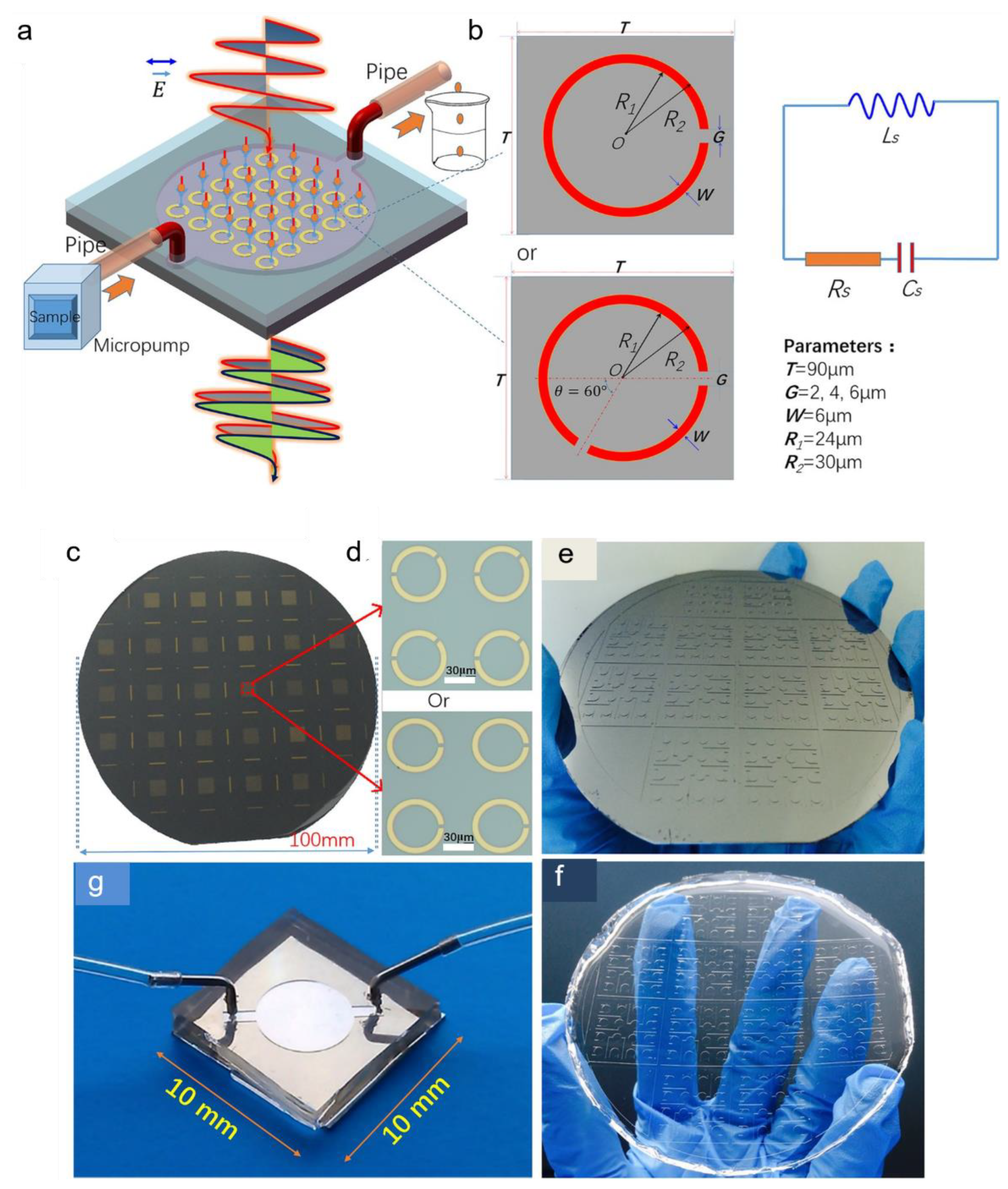
| References | Advantages/Disadvantages | Target Analyte | Sensor Configuration | Sensitivity | Frequency (f)/Analyte Concentration Range/Limit of Detection (LOD) |
|---|---|---|---|---|---|
| [21] | (+) Easy to fabricate at low cost. | biotin and streptavidin | Copper (Cu), Nickel (Ni), and gold (Au) printed on PCB | - | f range: 10.64 GHz to 10.84 GHz |
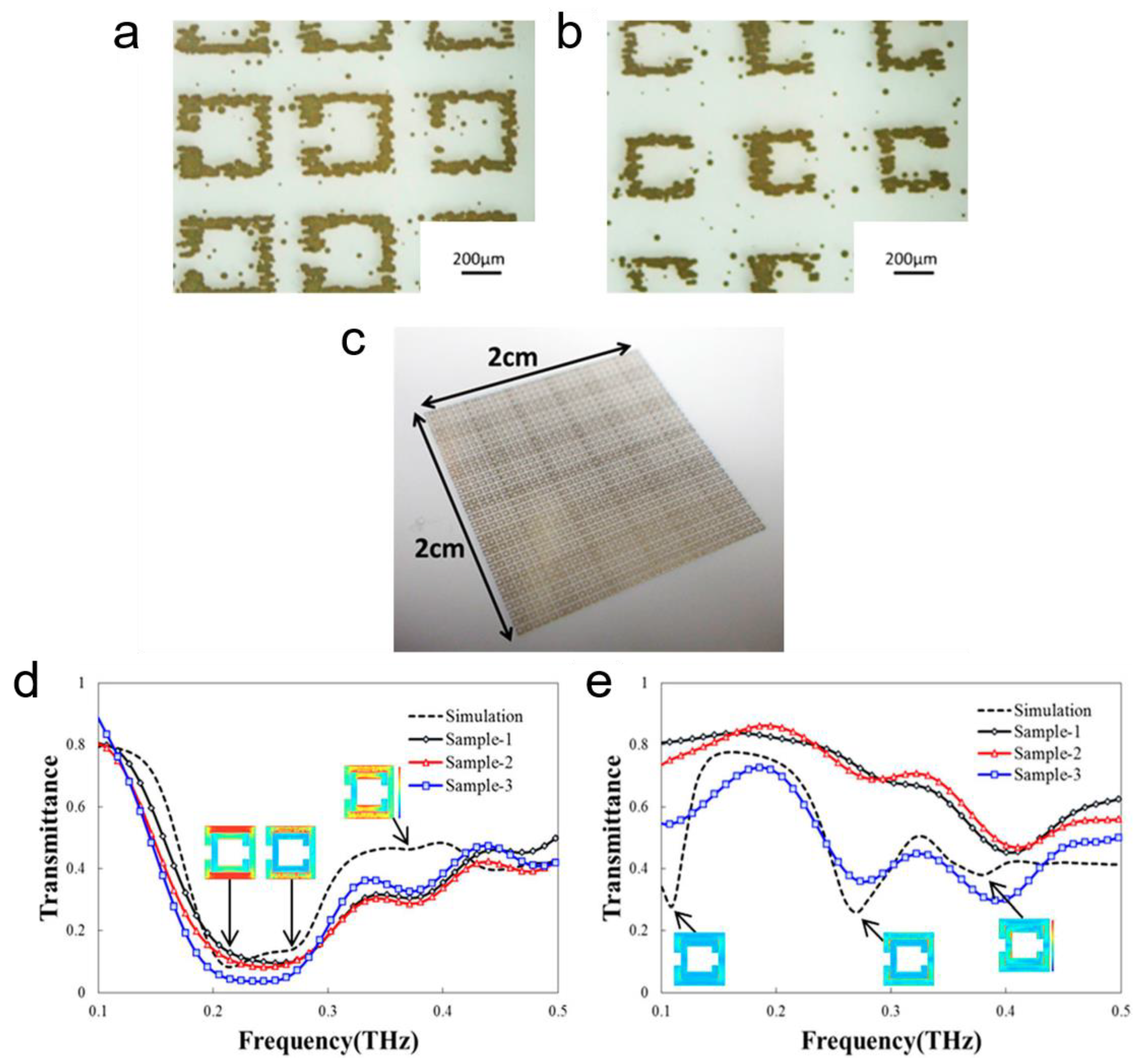
| [22] | (+) Low cost and easy inject printing-based fabrication | No specific analyte stated | Ag nanoparticles on paper and plastic substrate. | - | f range: 0.1 THz to 0.5 THz |
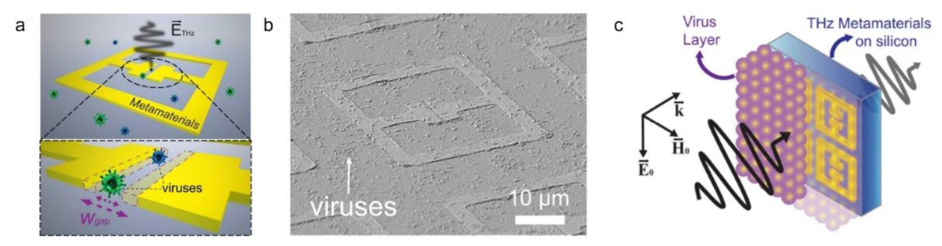
| [24] | (+) Minimal number of virus particles can be detected efficiently (-) Sophisticated e-beam lithography was used to fabricate the structure | 60 nm of PRD1 virus and 30 nm of MS2 virus | Metamaterial structure formed by 3 nm-thick Cr followed by 97 nm-thick gold | 6 GHz⋅μm2/particle to 80 GHz⋅μm2/particle | f range: 0.5 THz to 1.5 THz |
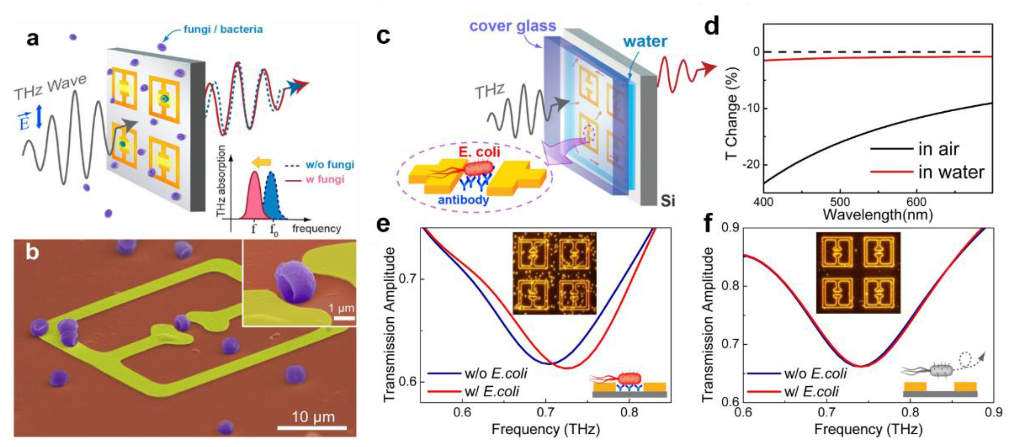
| [25] | (+) Faster detection in both air and aqueous environments (+) Can detect small number of microorganisms (-) Sophisticated e-beam evaporation-based metal deposition and photolithography | Yeasts and Escherichia coli BL21 (DE3), Neurospora sitophila (neurospora) and Aspergillus niger (niger) | Cr (2 nm) and Au (98 nm) metal films deposited on Si substrate | ~11.6 GHz/number density | f range: 0.5 THz to 3 THz LOD: 107 units/mL |
| [29] | (+) Higher sensitivity for four LC resonator-based SRRs as compared to a single LC resonator | Bovine Serum Albumin | Aluminium layer deposition by metal evaporation method | 85 GHz/RIU | f range: 0.2 THz to 1.2 THz LOD: 1.5 μmol/L |
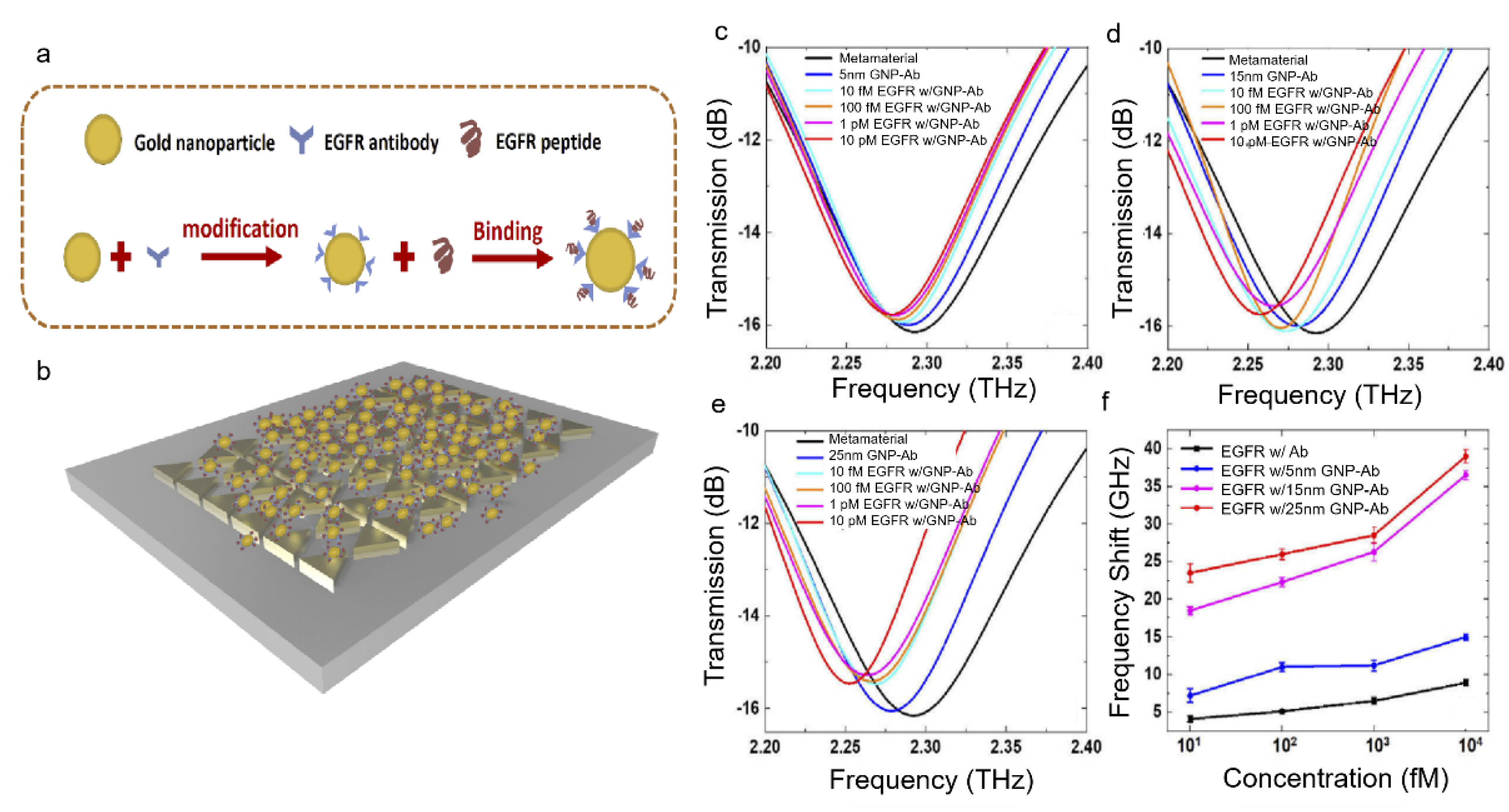
| [30] | (+) Enhanced sensitivity by adding AuNPs | The epidermal growth factor receptor (EGFR) antibody | Cr (20 nm) and Au (100 nm) bilayer film coated with AuNPs and arranged in a bow-tie configuration | 1.5 to 3.9 GHz/pM | f range: 2.2 THz to 2.4 THz Conc. Range: 10 fM to 10 pM |
| [33] | (+) Better performance because of the SiNx Film as compared to the bare Si substrate | Doped and undoped protein thin films (silk fibroin) | 200 nm gold patterned on 400 nm thick SiNx film deposited on Si wafer | 4.05 × 10⁻² GHz/nm. | f range: 0.1 THz to 1.2 THz |
| [34] | (+) High Q factor | Alpha-fetoprotein (AFP) and Glutamine transferase isozymes II (GGT-II) | The 200-nm thickness of gold on the Si wafer | 3.8 GHz/(mu/mL) for GGT-II and 562.6 GHz/(μg /mL) for AFP | f range: 0.4 THz to 1.2 THz |
| [39] | (+) FOM > 330 (+) Sensitivity several folds higher than the conventional plasmonic sensor | Streptavidin-biotin | Au nanorod on alumina matrix | >30,000 nm/RIU | f range: 200 THz to 749 THz LOD: 300 nM |
| [40] | (+) high FOM of 590 (+) capable of detecting lower molecular-weight (<500 Da) biomolecules | Biotin, BSA | gold–Al2O3 and grating-coupled hyperbolic metamaterial structure | 30,000 nm/RIU | f range: 150 THz to 600 THz Conc. Range: 10 pM to 1 µM |
| References | Advantages/Disadvantages | Target Analyte | Sensor Configuration | Sensitivity | Frequency (f)/Analyte Concentration Range/Limit of Detection (LOD) |
|---|---|---|---|---|---|
| [56] | (+) Hot spot region to enhance the plasmonic molecular coupling and improve sensitivity | CO2 and C4H10 | A gap between two gold electrodes | 2.92 × 10⁻⁴ ppm−1. | f range: 60 THz to 150 THz Conc. range: 20 to 388 ppm LOD: 20 ppm |
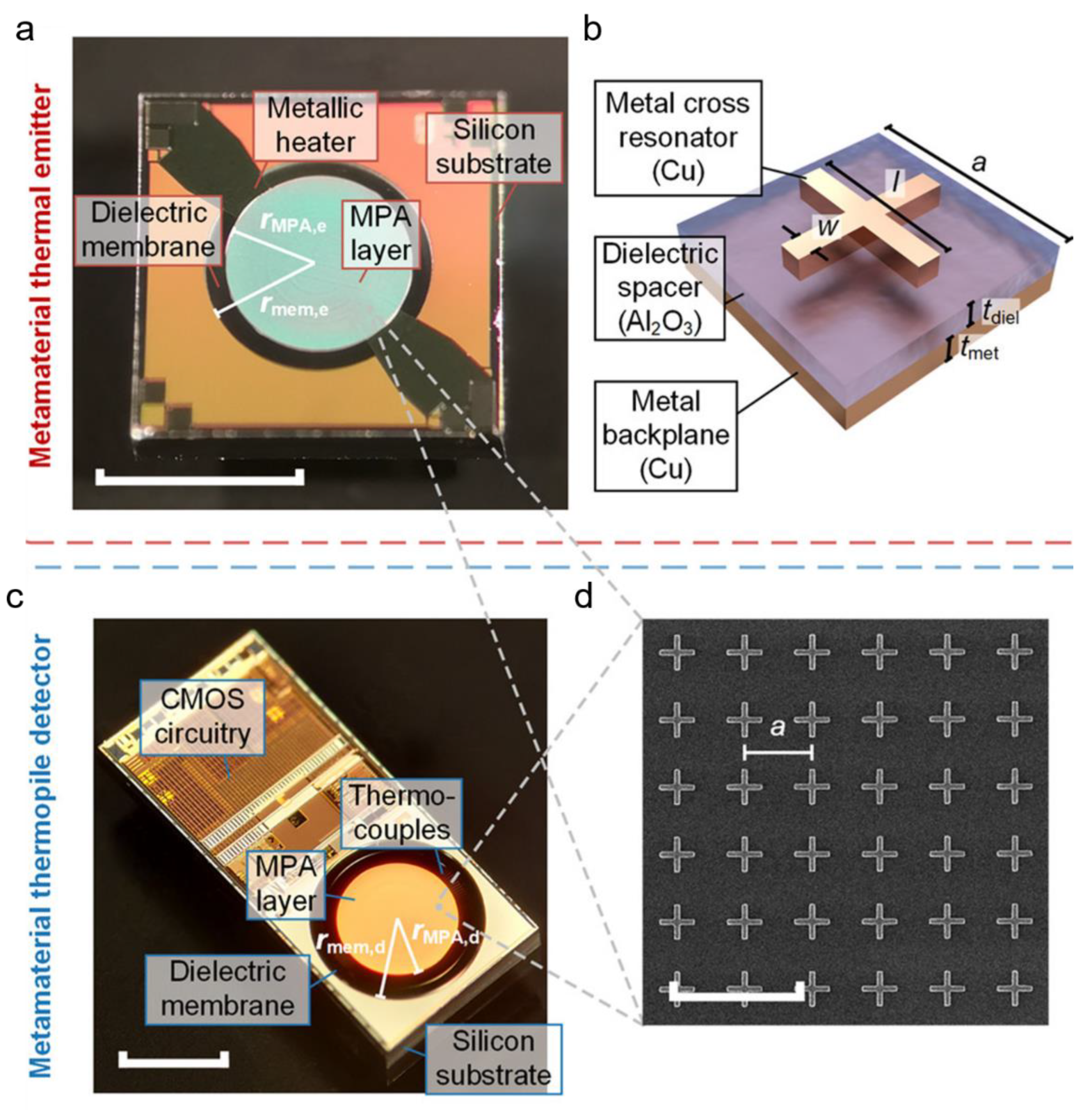
| [58] | (+) compact (+) sensitive (+) Energy-efficient gas detection (+) cascading the spectral responses of MPAs on the emitter and the detector to match the narrow absorption band of the target gas (+) highly scalable due to monolithic integration of MPAs into CMOS devices | CO2 | Gold-coated Si spacer on a PCB board | 22.4 ± 0.5 ppm·Hz−0.5 | Conc. range: 0 to 5000 ppm |
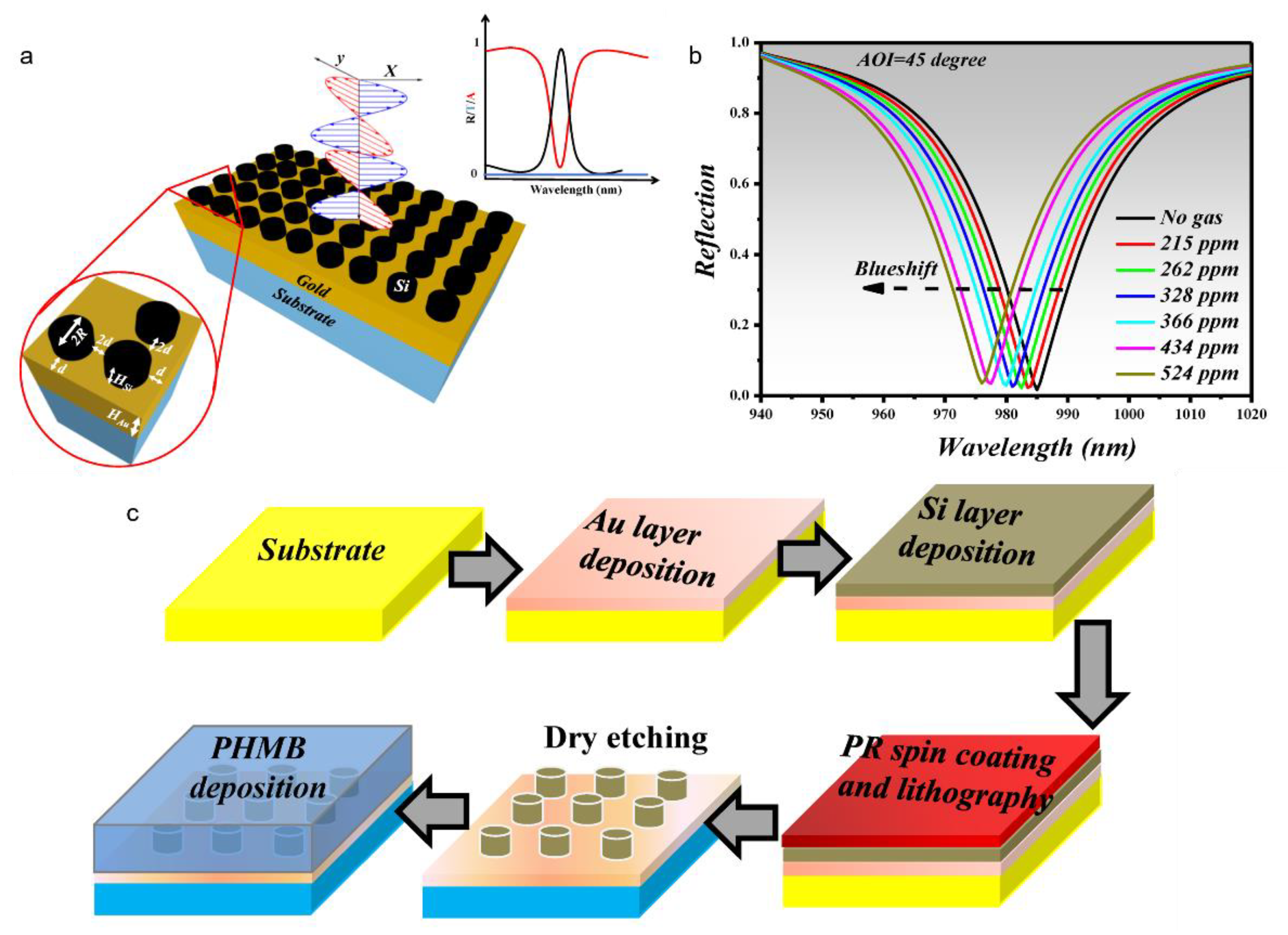
| [62] | (+) Wide detection range (-) Limited to numerical analysis and lacks physical implementation | CO2 | Nano-cylindrical meta-atoms on a gold layer deposited on a quartz substrate | 17.3 pm/ppm | f range: 294 THz to 319 THz Conc. range: 0 to 524 ppm |
| [63] | (+) Fabricated by a low-cost CMOS MEMS technology (+) A high-quality factor of 15.7 (+) features temperature-stable and angular-independent emission characteristics (+) a 5-fold increase in relative sensitivity compared to the conventional blackbody emitter | CO2 | a cross-shaped top Cu resonator was separated from a Cu backplane by means of a dielectric spacer layer (Al2O3) | 1.7 × 10⁻⁴ %/ppm | Conc. range: 0 to 50,000 ppm |
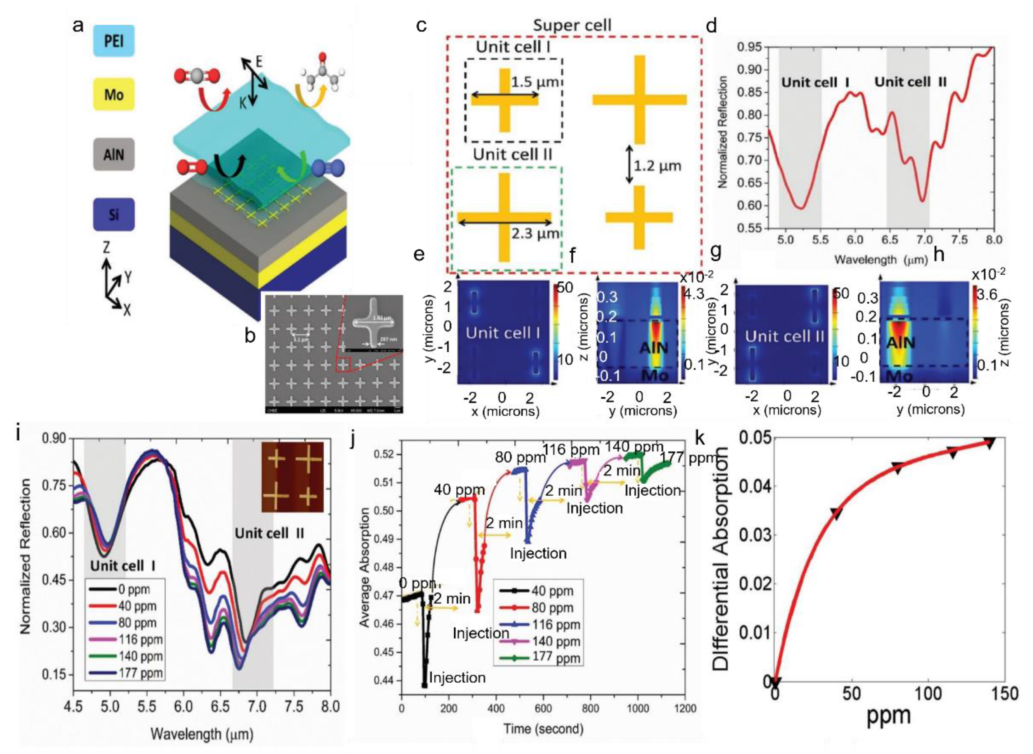
| [65] | (+) Two wavelength-based dual-mode multiplexed gas sensing (+) fast response time (≈2 min) | CO2 | polyethylenimine (PEI) polymer spun coated on AlN-Mo-Si | 500 nm/RIU | Conc. range: 0 to 177 ppm LOD: 40 ppm |
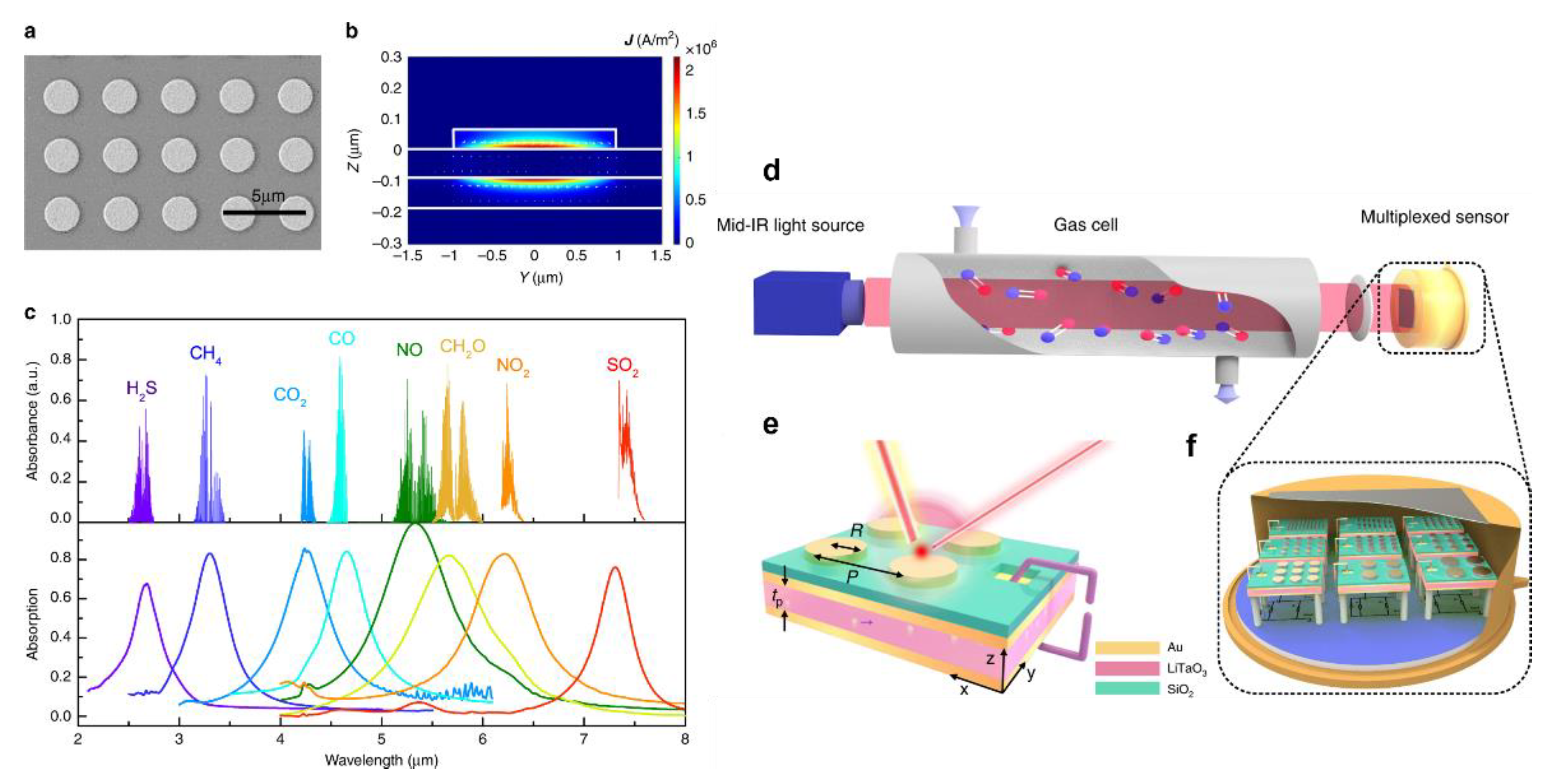
| [68] | (+) Multiplexed sensing of gases in a mixture | H2S, CH4, CO2, CO, NO, CH2O, NO2, SO2 | From the top to the bottom are: Au nanodisk antenna, the 80 nm silicon dioxide spacer, the Au backplate, the 75 µm lithium tantalate (LT) substrate and the 100 nm Au bottom electrode | Not stated | Conc. range: 0 to 20,000 ppm LOD: 489, 63, 2, 11, 17, 27, 54 and 104 ppm for H2S, CH4, CO2, CO, NO, CH2O, NO2 and SO2 |
| [72] | (+) Highly reliable, re-usable and selective (+) a new signature evolving at 300 MHz | NO2 | Fe3O4 nanoparticles on two square ring-shaped slots | 0.2 MHz/ppm | f range: 200 MHz to 800 MHz Conc. range: 0 to 110 ppm |
| [75] | (+) the presence or absence of H2 can be monitored by direct visual inspection (+) response time of only 10 s (+) low-cost fabrication using a simple electrochemical technique | H2 and N2 | Bimetallic Au/Pd nanorod on a glass substrate | - | f range: 333 THz to 750 THz LOD: 1% H2 |
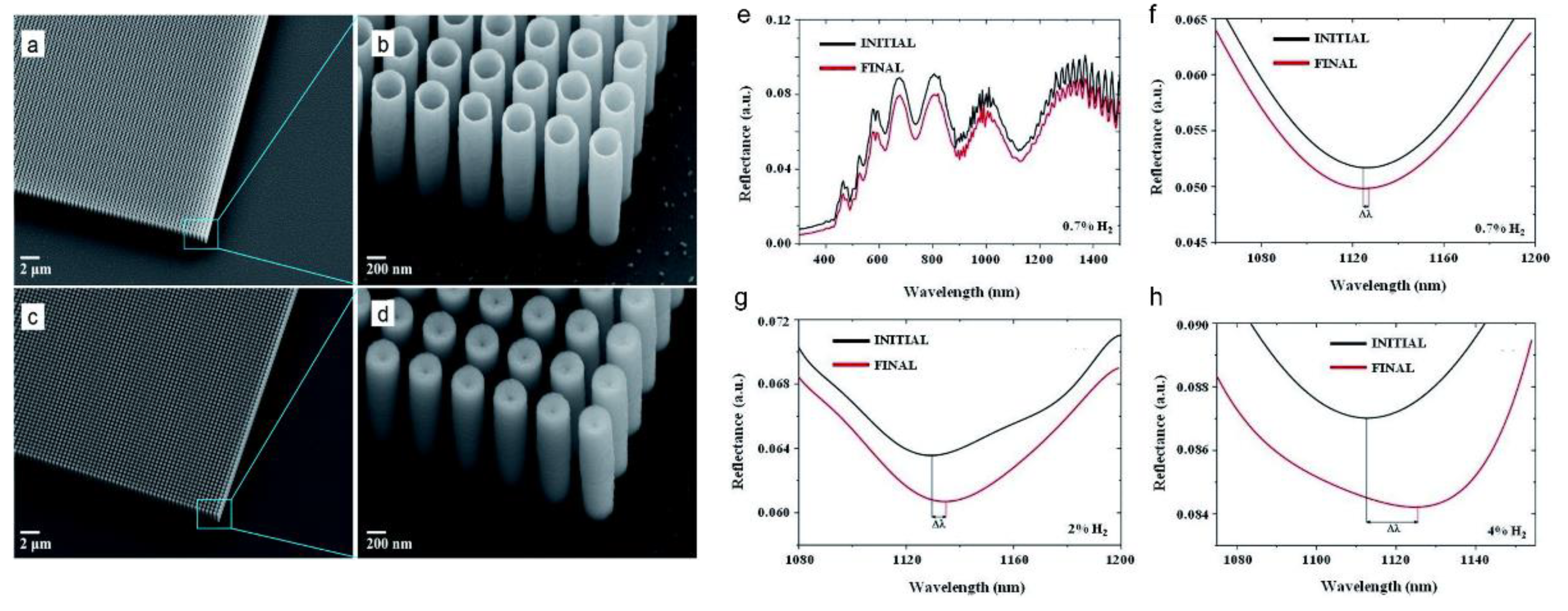
| [79] | (+) large sensing area (+) high sensitivity at room temperature (+) fast response in 10 min (-) sophisticated ion reactive etching and atomic deposition layer | H2 | Aluminium-doped Zinc oxide (AZO nanotubes) on SiO2/Si substrate | 0.0006 a.u./% | f range: 250 THz to 333 THz Conc. range: 0.7 to 4% LOD: 0.7% |
| References | Advantages/Disadvantages | Target Analyte | Sensor Configuration | Sensitivity | Frequency (f)/Analyte Concentration Range/Limit of Detection (LOD) |
|---|---|---|---|---|---|
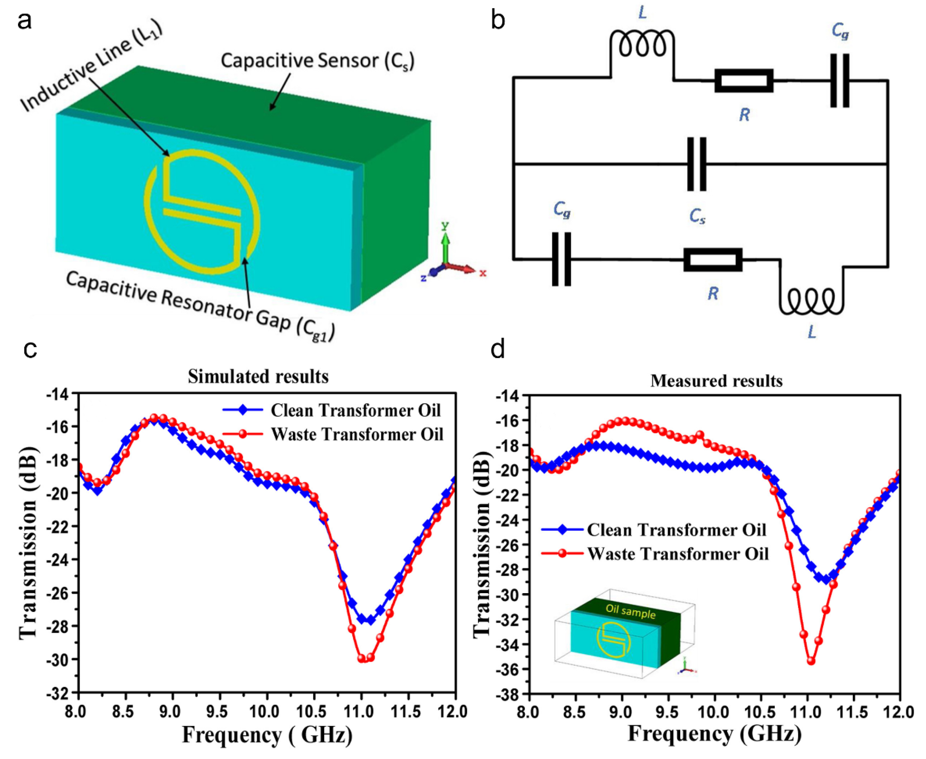
| [91] | (+) real-time (+) fast (+) low cost (+) durable (+) accurate detection | Clean and waste transformer oil, Corn, olive and cotton oils, branded and unbranded diesels, aniline-doped ethyl-alcohol and benzene-doped carbon tetrachloride | Copper pad on both front and backside of FR-4 substrate | 250 MHz/ 0.11 εr | f range: 8 GHz to 12 GHz LOD: Not stated (detection was based on separation of resonance peaks) |
| [93] | (+) Linear relationship between pesticide concentrations and transmission amplitudes | 2,4-dichlorophenoxy acetic and chlorpyrifos solutions | multiwalled CNT arrays on a silicon substrate | 1.38 × 10⁻²/ppm from 1–10 ppm and 3.0 × 10⁻³/ppm over 10 ppm | Conc. range: 1–10 ppm and 10–80 ppm |
| [97] | (+) improved sensitivity due to the integration of inter-digital capacitor (IDC) topology (+) better frequency resolution compared to existing SRRs (+) simple design (+) easy fabrication (+) economical | Glucose | Copper SRR made on Rogers RT6006 substrate and integrated with PDMS microfluidic channel | 0.026 MHz/(mg/dL) | f range: 3 GHz to 5 GHz Conc. range: 0–5000 mg/dL |
| [98] | (+) miniaturised (24*15*0.6 mm3) (+) reusable (+) label-free (+) non-destructive (+) smaller sample volume (4 µL) (+) multi-band sensing (+) better linearity in ethanol sensing (−2.80%) | Ethanol-water mixture | Copper coated with 3.5 µm thick Ni/Au layer on Rogers 4003c substrate (0.203 mm thick) | 2.1 × 10⁶ Hz/% | Conc. range: 0–100% of ethanol in water-ethanol mixture |
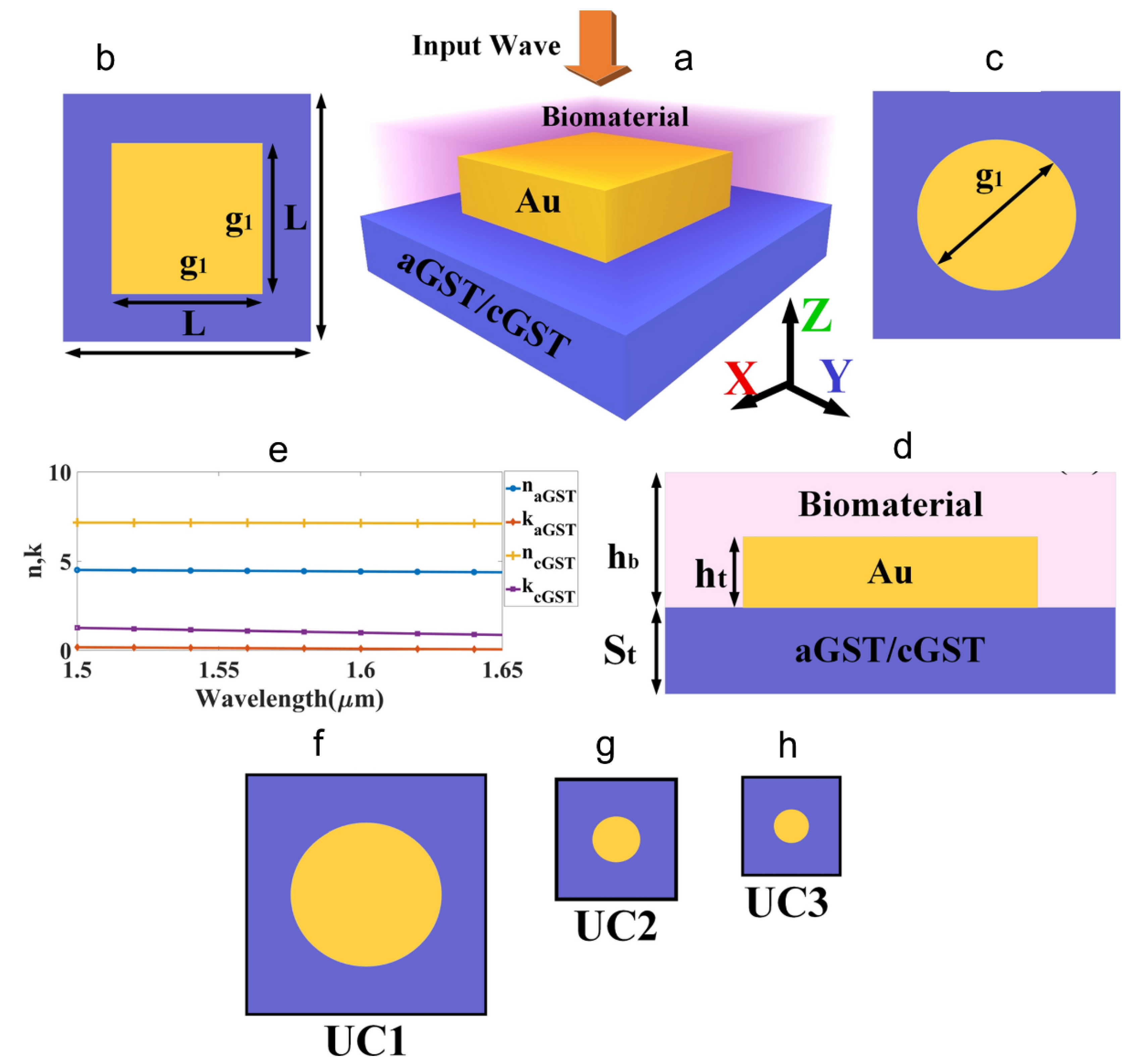
| [99] | (+) Tunable response | Haemoglobin, urine | amorphous GST (aGST) and crystalline GST (cGST) in different design structures | 825–1795 nm/RIU when tested on haemoglobin, and 1000–2333 nm/RIU when tested on urine | f range: 181 THz to 200 THz Conc. range: 10–40 g/L for haemoglobin, and 0–10 mg/dL for urine |
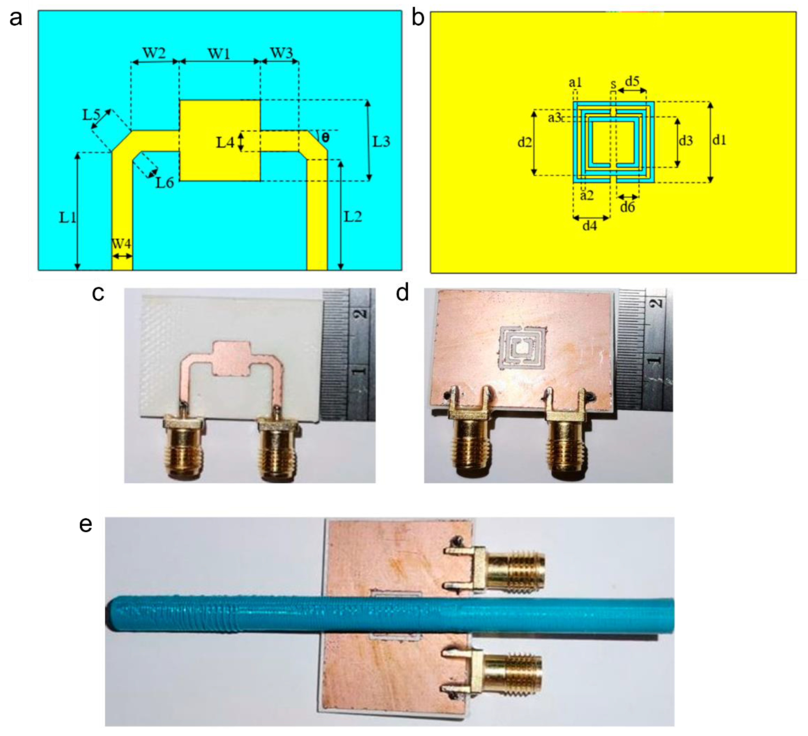
| [101] | (+) Optimised asymmetric electric split-ring resonator (AESRR) topology (+) distinguish liquids and solid dielectric materials with bigger frequency shift and higher sensitivity. (+) low-cost (+) real-time (+) high sensitivity (+) high robustness | Peanut oil, Corn oil, Sunflower seed oil, Soybean oil, Isopropyl alcohol, ethyl acetate, ethanol | Copper pad on FR-4 substrate | 0.612 | LOD: Not stated (detection was based on separation of resonance peaks) |
| [102] | (+) compact design on a single PCB (+) low cost (+) contactless (+) reusable (+) easy to fabricate | Ethanol–water mixture | Copper pad on FR-4 substrate | 0.57 | Conc. range: 0–100% of ethanol in water-ethanol mixture |
| [103] | (+) high sensitivity detection of scattered data (+) adequate penetration depth | Glucose | Copper pad on FR-4 substrate | 0.0125 dB/(mg/dL) | f range: 2.2 GHz to 3.8 GHz Conc. range: 100–300 mg/dl |
| [104] | (+) Ultralow limit of detection | anti-BSA | Al coated periodic nanopillar arrays | 0.14 ng/mL | f range: 333 THz to 1000 THz Conc. range: 0.001–1000 ng/mL LOD: 1 pg/mL |
| [105] | (+) No pretreatment required | Vitamin D | Au coated cross and star shaped nanostructures on silicon substrate | 500–800 nm/RIU | LOD: 86 pM |
Publisher’s Note: MDPI stays neutral with regard to jurisdictional claims in published maps and institutional affiliations. |
© 2022 by the authors. Licensee MDPI, Basel, Switzerland. This article is an open access article distributed under the terms and conditions of the Creative Commons Attribution (CC BY) license (https://creativecommons.org/licenses/by/4.0/).
Share and Cite
Tabassum, S.; Nayemuzzaman, S.; Kala, M.; Kumar Mishra, A.; Mishra, S.K. Metasurfaces for Sensing Applications: Gas, Bio and Chemical. Sensors 2022, 22, 6896. https://doi.org/10.3390/s22186896
Tabassum S, Nayemuzzaman S, Kala M, Kumar Mishra A, Mishra SK. Metasurfaces for Sensing Applications: Gas, Bio and Chemical. Sensors. 2022; 22(18):6896. https://doi.org/10.3390/s22186896
Chicago/Turabian StyleTabassum, Shawana, SK Nayemuzzaman, Manish Kala, Akhilesh Kumar Mishra, and Satyendra Kumar Mishra. 2022. "Metasurfaces for Sensing Applications: Gas, Bio and Chemical" Sensors 22, no. 18: 6896. https://doi.org/10.3390/s22186896