Modeling and Analysis of Capacitive Relaxation Quenching in a Single Photon Avalanche Diode (SPAD) Applied to a CMOS Image Sensor

Abstract
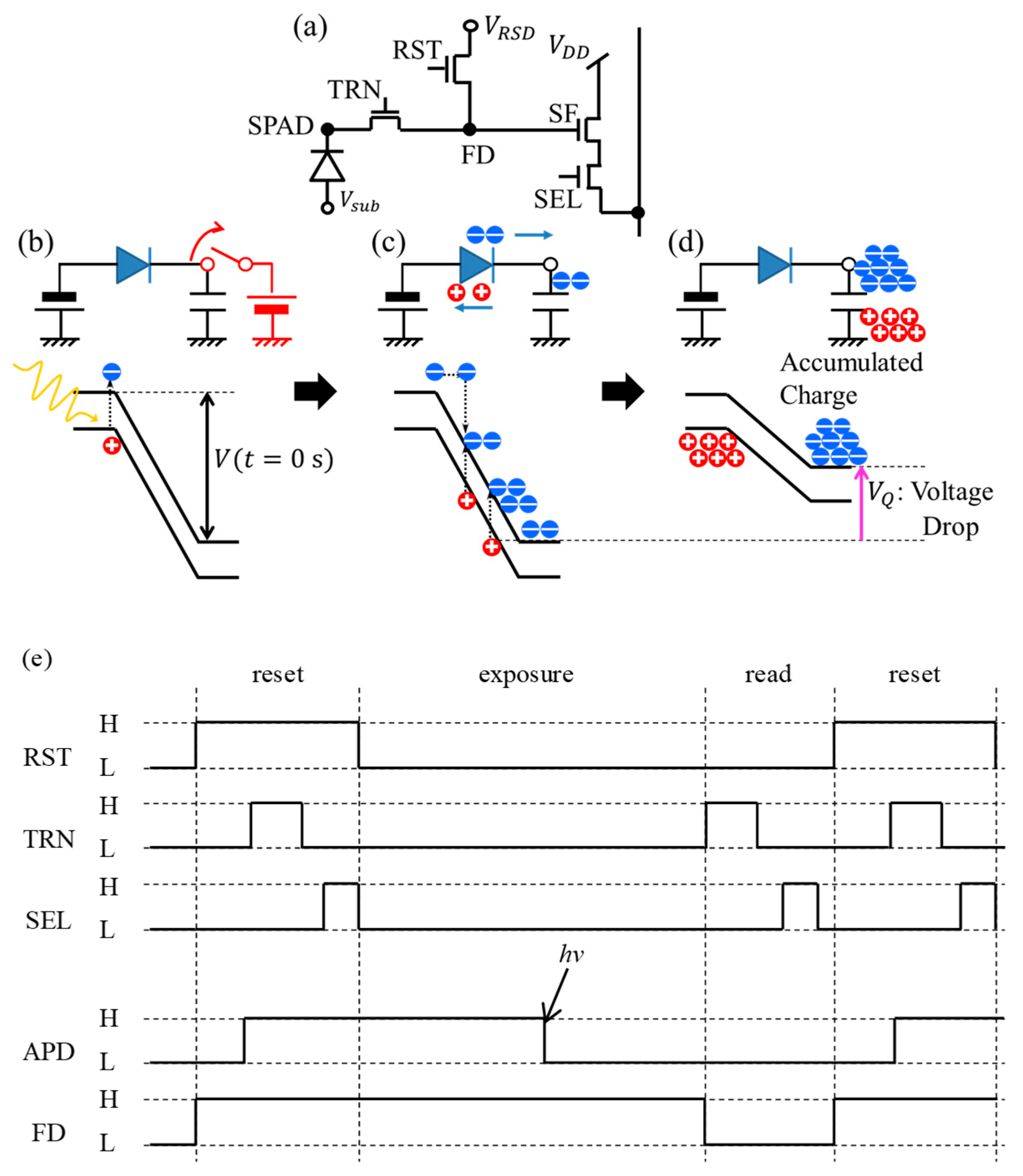
:1. Introduction
2. Modeling of Capacitive Relaxation Quenching
3. Results
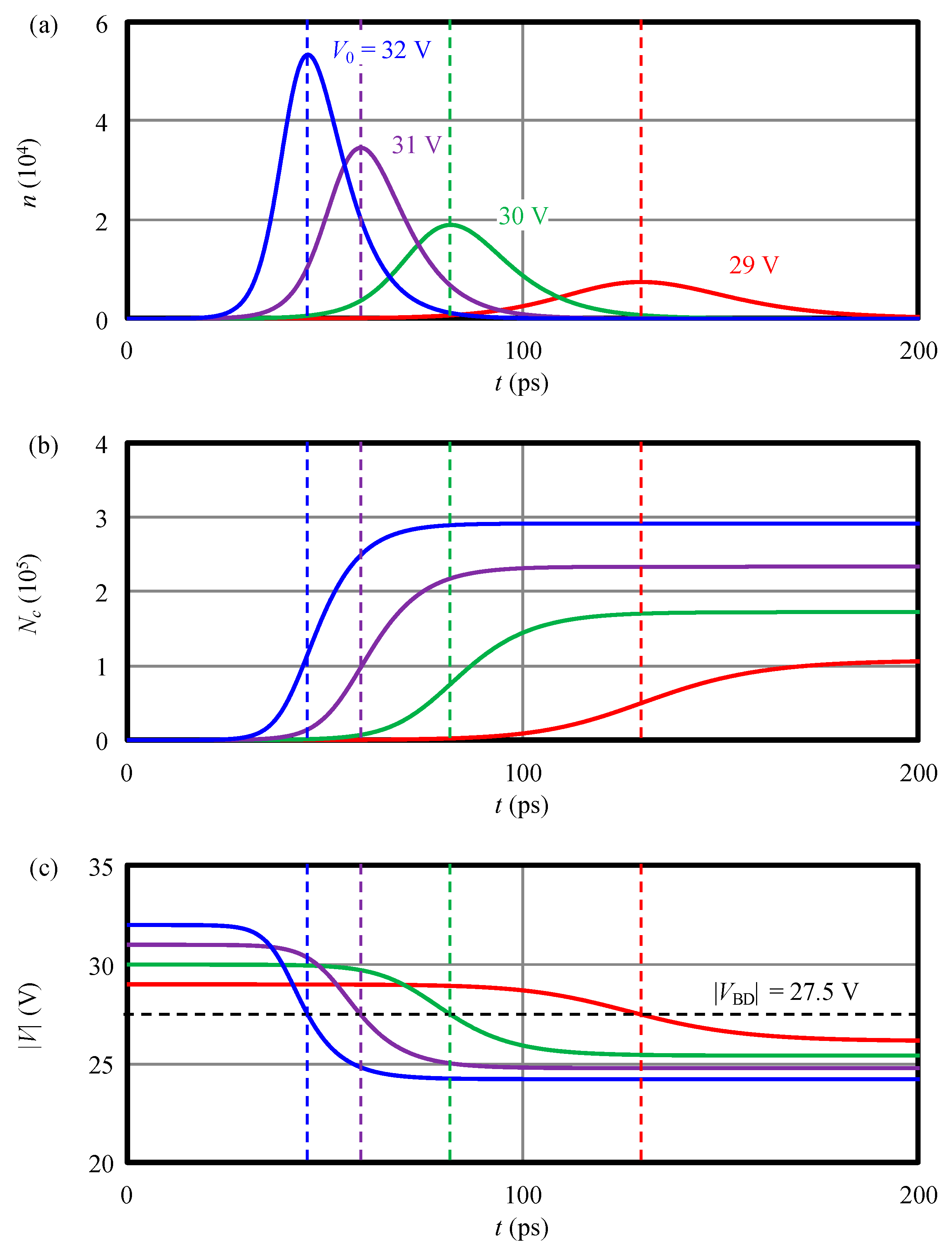
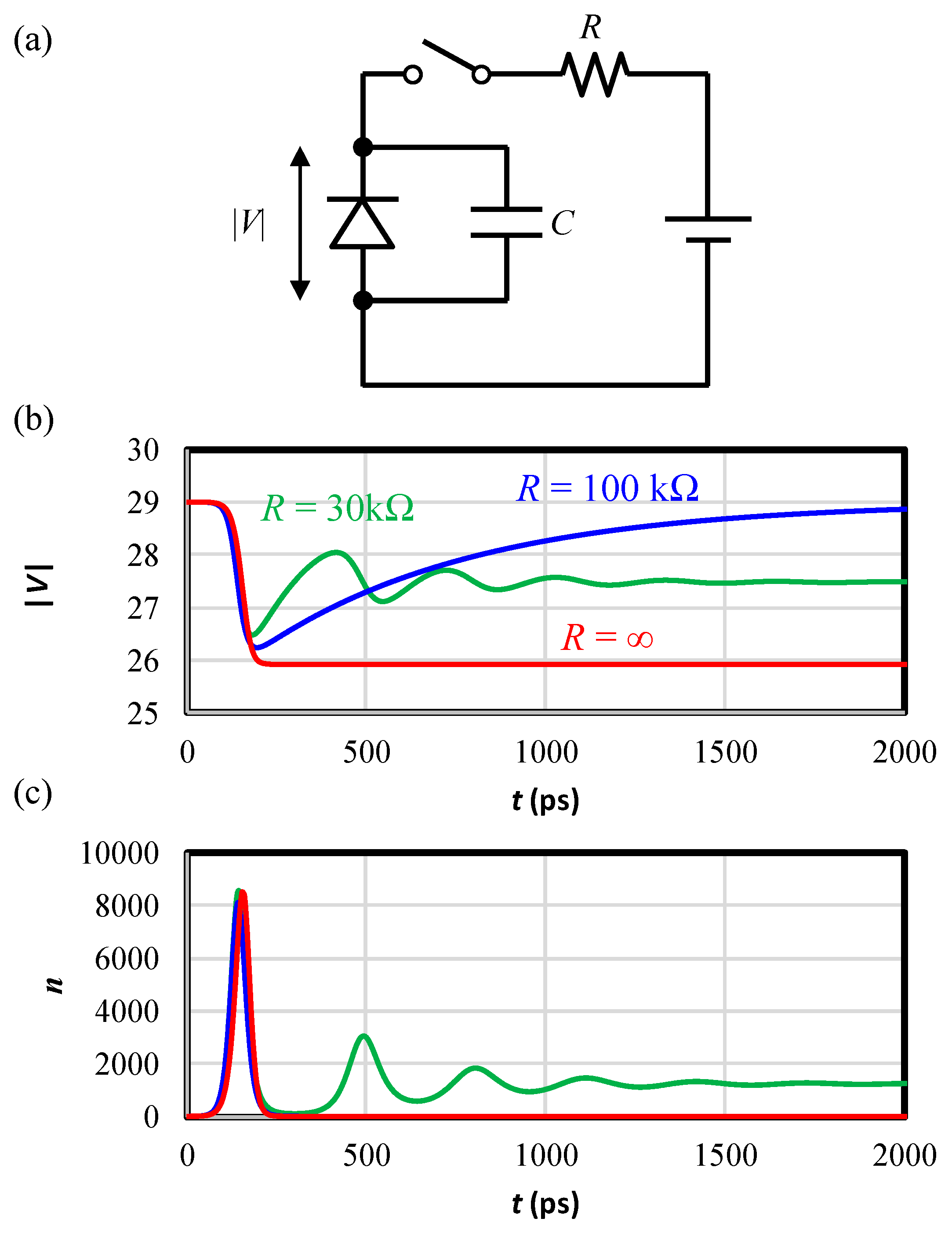
3.1. Numerical Calculation
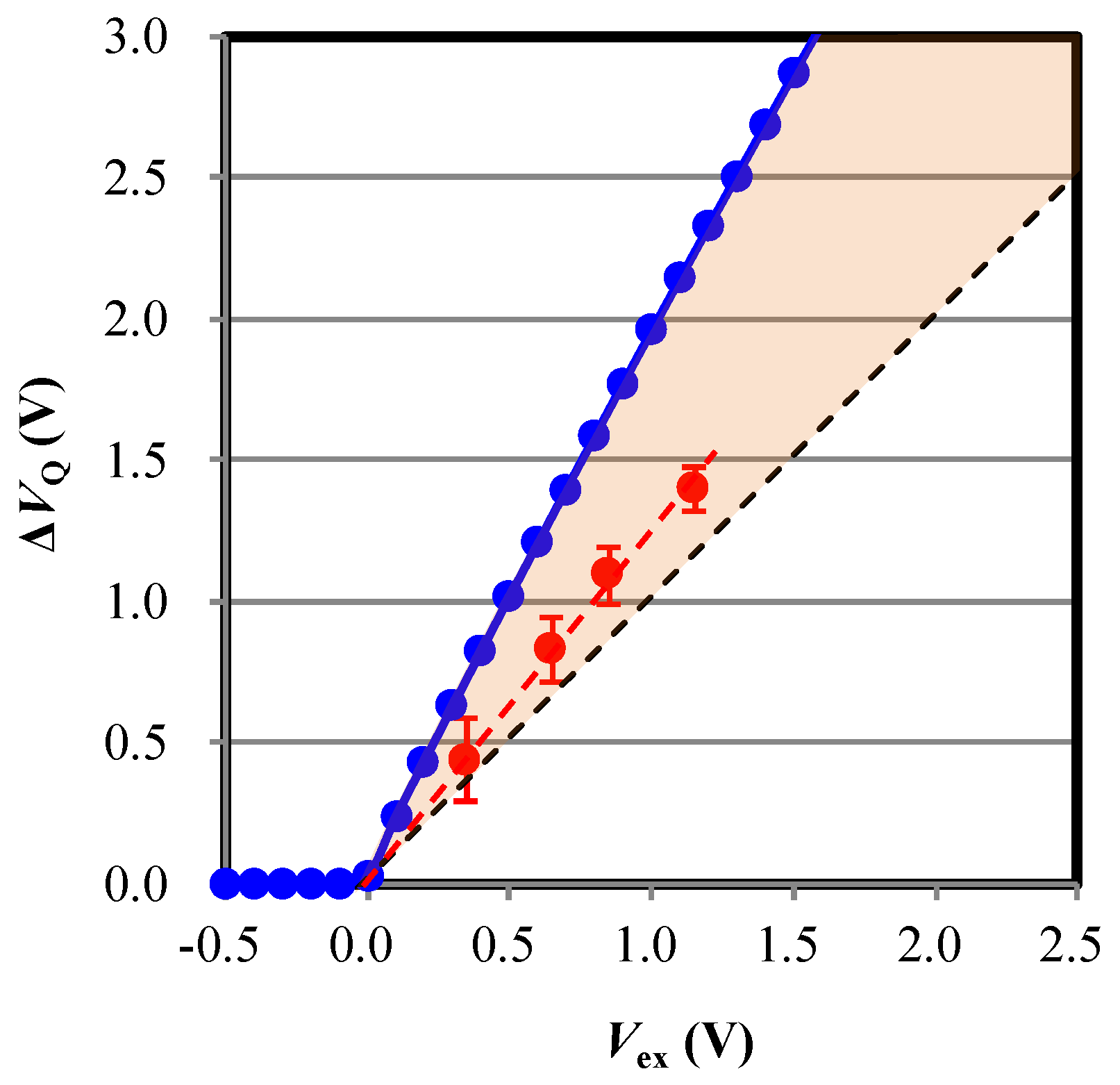
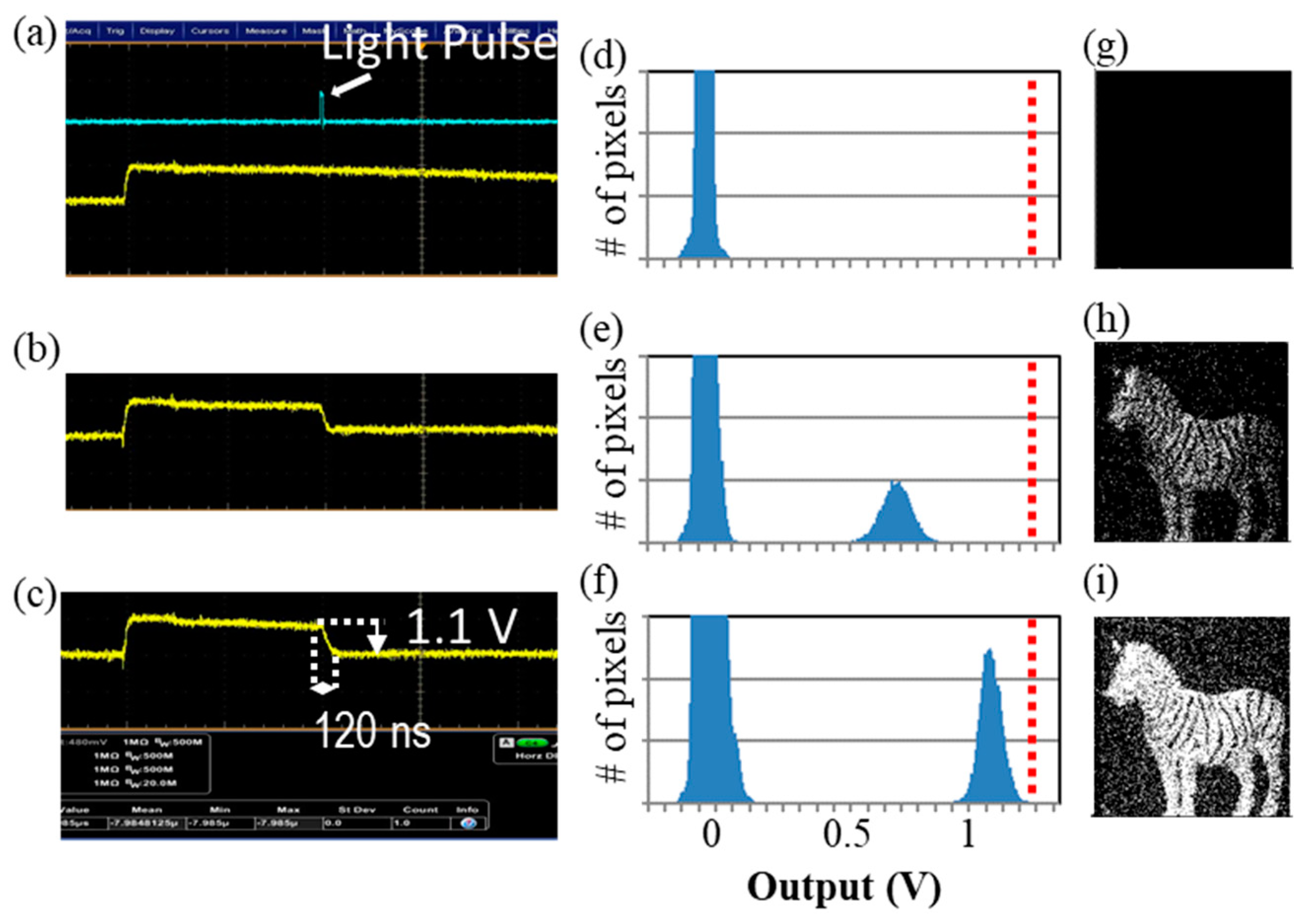
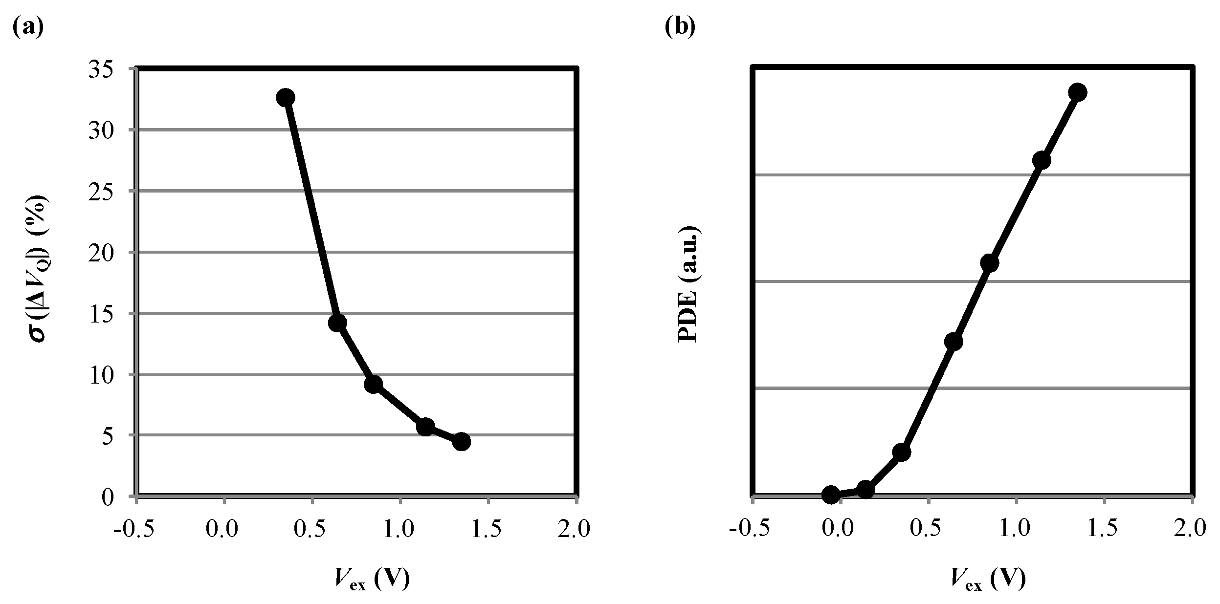
3.2. Experimental Results
4. Discussion
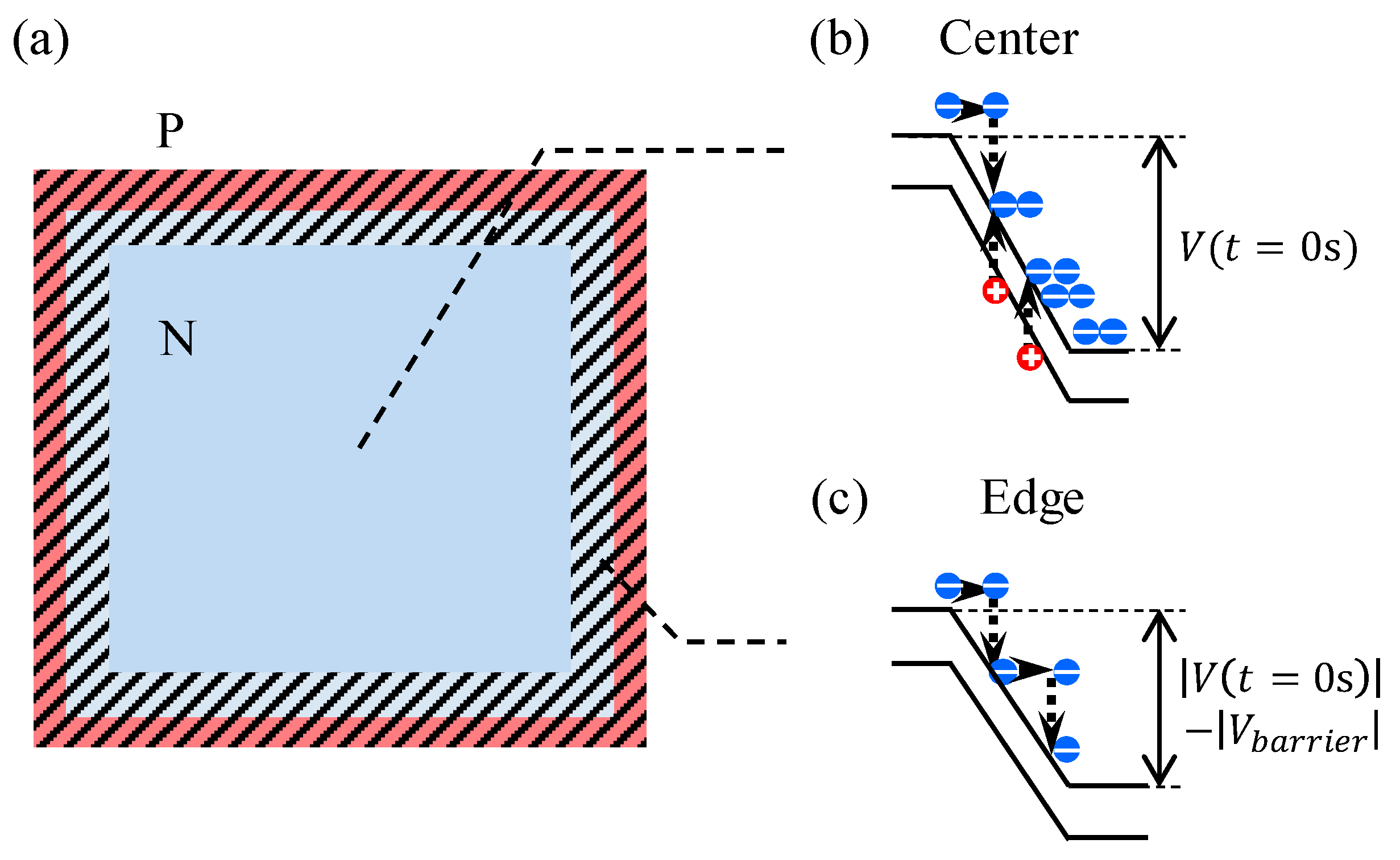
4.1. Breakdown Voltage as an Equilibrium Point of the Dynamical System
4.2. Difference of between Simulation and Experiment
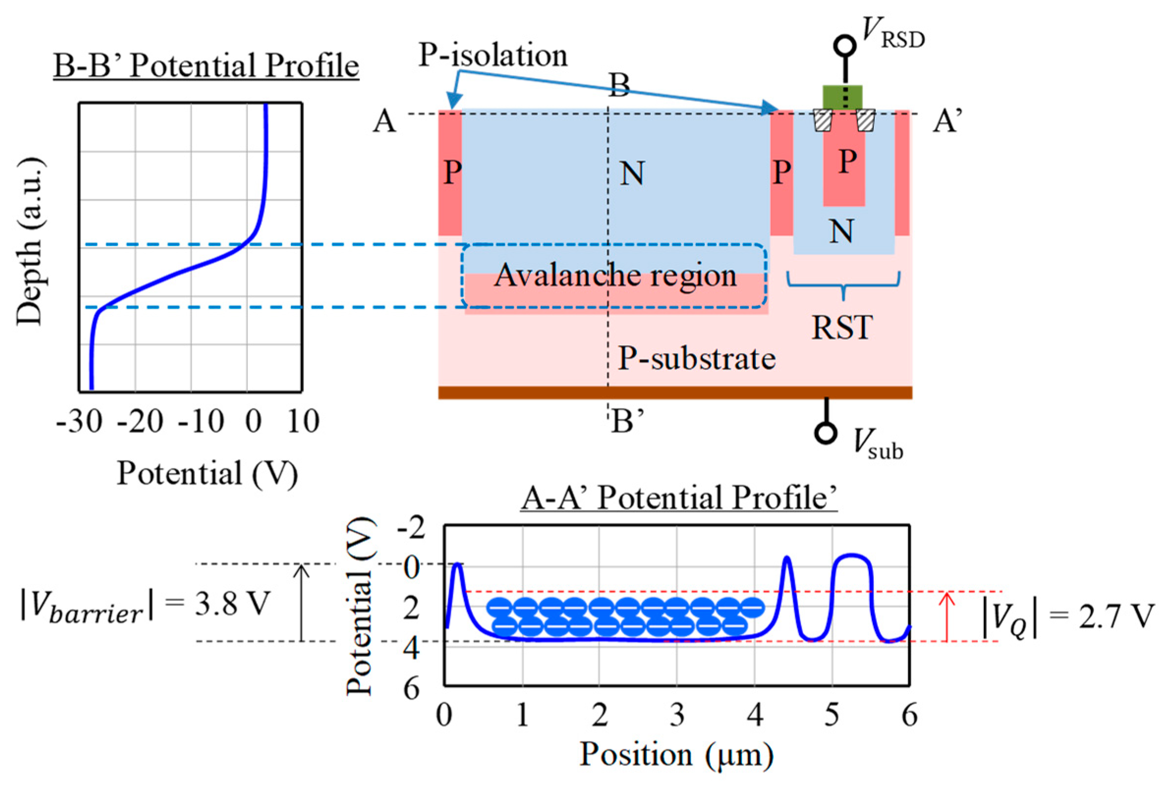
4.3. The Mechanism of Resistive Quenching
5. Conclusions
Author Contributions
Funding
Conflicts of Interest
References
- Cova, S.; Longoni, A.; Andreoni, A. Toward picosecond resolution with single-photon avalanche diodes. Rev. Sci. Instr. 1981, 52, 408–412. [Google Scholar] [CrossRef] [Green Version]
- Charbon, E. Monolithic Single-Photon Avalanche Diodes: SPADs. In Single Photon Imaging; Springer: Heidelberg, Germany; Dordrecht, The Netherlands; London, UK; New York, NY, USA, 2011; pp. 123–158. [Google Scholar]
- Charbon, E. Single-photon imaging in CMOS. In Proceedings of the SPIE, San Diego, CA, USA, 1–5 August 2010; Volume 7780, p. 77801D-1. [Google Scholar]
- Rochas, A.; Gani, M.; Furrer, B.; Besse, P.A.; Popovic, R.S.; Ribordy, G.; Gisin, N. Single photon detector fabricated in a complementary metal–oxide–semiconductor high-voltage technology. Rev. Sci. Ins. 2003, 74, 3263–3270. [Google Scholar] [CrossRef] [Green Version]
- Dutton, N.A.W.; Gyongy, I.; Parmesan, L.; Gnecchi, S.; Calder, N.; Rae, B.R.; Pellegrini, S.; Grant, L.A.; Henderson, R.K. A SPAD-Based QVGA Image Sensor for Single-Photon Counting and Quanta Imaging. IEEE Trans. Electron Devices 2016, 63, 189–196. [Google Scholar] [CrossRef] [Green Version]
- Dutton, N.A.; Abbas, T.A.; Gyongy, I.; Henderson, R.K. Extending the Dynamic Range of Oversampled Binary SPAD Image Sensors. In Proceedings of the International Image Sensor Workshop (IISW), Hiroshima, Japan, 30 May–2 June 2017; p. P07. [Google Scholar]
- Henderson, R.K.; Johnston, N.; Hutchings, S.W.; Gyongy, I.; Abbas, T.A.; Dutton, N.; Tyler, M.; Chan, S.; Leach, J. A 256 × 256 40nm/90nm CMOS 3D-Stacked 120dB Dynamic-Range Reconfigurable Time-Resolved SPAD Imager. In Proceedings of the IEEE Int. Solid-State Circuits Conf. (ISSCC) Dig. Tech. Papers, San Francisco, CA, USA, 17–21 February 2019; pp. 106–108. [Google Scholar]
- Niclass, C.; Sergio, M.; Charbon, E. SPIE Opt. A single photon avalanche diode array fabricated in 0.35-μm CMOS and based on an event-driven readout for TCSPC experiments. In Proceedings of the SPIE, Atlanta, GA, USA, 25 October 2006; Volume 6372, p. 63720S. [Google Scholar]
- Perenzoni, M.; Massari, N.; Perenzoni, D.; Gasparini, L.; Stoppa, D. A 160 × 120 Pixel Analog-Counting Single-Photon Imager with Time-Gating and Self-Referenced Column-Parallel A/D Conversion for Fluorescence Lifetime Imaging. IEEE J. Solid-State Circuits 2016, 51, 155–167. [Google Scholar]
- Zhang, C.; Lindner, S.; Antolovic, I.M.; Wolf, M.; Charbon, E. A CMOS SPAD Imager with Collision Detection and 128 Dynamically Reallocating TDCs for Single-Photon Counting and 3D. Sensors 2018, 18, 4016. [Google Scholar] [CrossRef] [PubMed] [Green Version]
- Takai, I.; Matsubara, H.; Soga, M.; Ohta, M.; Ogawa, M.; Yamashita, T. Single-Photon Avalanche Diode with Enhanced NIR-Sensitivity for Automotive LIDAR Systems. Sensors 2016, 16, 459. [Google Scholar] [CrossRef] [PubMed]
- Hirose, Y.; Koyama, S.; Ishii, M.; Saitou, S.; Takemoto, M.; Nose, Y.; Inoue, A.; Sakata, Y.; Sugiura, Y.; Kabe, T.; et al. A 250 m Direct Time-of-Flight Ranging System Based on a Synthesis of Sub-Ranging Images and a Vertical Avalanche Photo-Diodes (VAPD) CMOS Image Sensor. Sensors 2018, 18, 3642. [Google Scholar] [CrossRef] [PubMed] [Green Version]
- Zhao, K.; You, S.; Cheng, J.; Lo, Y.H. Self-quenching and self-recovering InGaAs/InAlAs single photon avalanche detector. Appl. Phys. Lett. 2008, 93, 153504. [Google Scholar] [CrossRef]
- Hayat, M.M.; Ramirez, D.A.; Rees, G.J.; Itzler, M.A. Modeling negative feedback in single-photon avalanche diodes. In Proceedings of the SPIE, Orlando, FL, USA, 25–29 April 2010; Volume 7681, p. 76810W-1. [Google Scholar]
- Zappalà, G.; Acerbi, F.; Ferri, A.; Gola, A.; Paternoster, G.; Regazzoni, V.; Zorzib, N.; Piemonteb, C. Study of the photo-detection efficiency of FBK High-Density silicon photomultipliers. J. Instrum. 2016, 11, P11010. [Google Scholar] [CrossRef]
- Mori, M.; Sakata, Y.; Usuda, M.; Yamahira, S.; Kasuga, S.; Hirose, Y.; Kato, Y.; Tanaka, T. A 1280x720 single-photon-detecting image sensor with 100dB dynamic range using a sensitivity-boosting technique. In Proceedings of the IEEE Int. Solid-State Circuits Conf. (ISSCC) Dig. Tech. Papers, San Francisco, CA, USA, 31 January–4 February 2016; pp. 120–121. [Google Scholar]
- Hirose, Y.; Koyama, S.; Okino, T.; Inoue, A.; Saito, S.; Nose, Y.; Ishii, M.; Yamahira, S.; Kasuga, S.; Mori, M.; et al. A 400x400-Pixel 6μm-Pitch Vertical Avalanche Photodiodes (VAPD) CMOS Image Sensor Based on 150ps-fast Capacitive Relaxation Quenching (RQ) in Geiger Mode for Synthesis of Arbitrary Gain Images. In Proceedings of the IEEE Int. Solid-State Circuits Conf. (ISSCC) Dig. Tech. Papers, San Francisco, CA, USA, 17–21 February 2019; pp. 104–105. [Google Scholar]
- Sze, S.M.; Gibbons, G. Avalanche breakdown voltages of abrupt and linearly graded pn junctions in Ge, Si, GaAs, and GaP. Appl. Phys. Lett. 1966, 8, 111–113. [Google Scholar] [CrossRef]
- Muller, R.S.; Kamins, T.I. Device Electronics for Integrated Circuits, 3rd ed.; Wiley: Hoboken, NJ, USA, 2003; p. 33. [Google Scholar]
- Chynoweth, A.G. Ionization Rates for Electrons and Holes in Silicon. Phys. Rev. 1958, 109, 1537–1540. [Google Scholar] [CrossRef]
- Overstraeten, R.V.; Man, H.D. Measurement of the Ionization Rates in Diffused Silicon p-n Junctions. Solid-State Electron. 1970, 13, 583–608. [Google Scholar] [CrossRef]
- Gnani, E.; Reggiani, S.; Rudan, M.; Baccarani, G. Extraction method for the impact-ionization multiplication factor in silicon at large operating temperatures. In Proceedings of the IEEE European Solid-State Device Research Conference, Bordeaux, France, 1–14 September 2020; pp. 227–230. [Google Scholar]
- Haitz, R.H. Model for the Electrical Behavior of a Microplasma. J. Appl. Phys. 1964, 35, 1370–1376. [Google Scholar] [CrossRef]
- Cova, S.; Ghioni, M.; Lacaita, A.; Samori, C.; Zappa, F. Avalanche photodiodes and quenching circuits for single-photon detection. Appl. Opt. 1996, 35, 1956–1976. [Google Scholar] [CrossRef] [PubMed]
- Oldham, W.; Samuelson, R.; Antognetti, P. Triggering Phenomena in Avalanche Diodes. IEEE Trans. Electron Devices 1972, ED-19, 1056–1060. [Google Scholar] [CrossRef]
- Sze, S.M.; Ng, K.K. Physics of Semiconductor Devices, 3rd ed.; Wiley: Hoboken, NJ, USA, 2007; pp. 105–106. [Google Scholar]
- Misawa, T. Negative Resistance in p-n Junctions under Avalanche Breakdown Conditions, Part II. IEEE Trans. Electron Devices 1966, ED-13, 143–151. [Google Scholar] [CrossRef]
- Spinelli, A.; Lacaita, A.L. Physics and Numerical Simulation of Single Photon Avalanche Diodes. IEEE Trans. Electron Devices 1997, 44, 1931–1943. [Google Scholar] [CrossRef] [Green Version]


| Meaning | Symbol | Value |
|---|---|---|
| Width of depletion region | W | 0.80 µm |
| Saturation velocity of electron [19] | vs,e | 1.02 × 107 cm /s |
| Saturation velocity of hole [19] | vs,h | 8.31 × 106 cm/s |
| Coefficients of impact ionization ratio [18] | 3.80 × 106 cm−1 | |
| 2.25 × 107 cm−1 | ||
| a | 1.75 × 10⁶ V/cm | |
| b | 3.26 × 10⁶ V/cm |
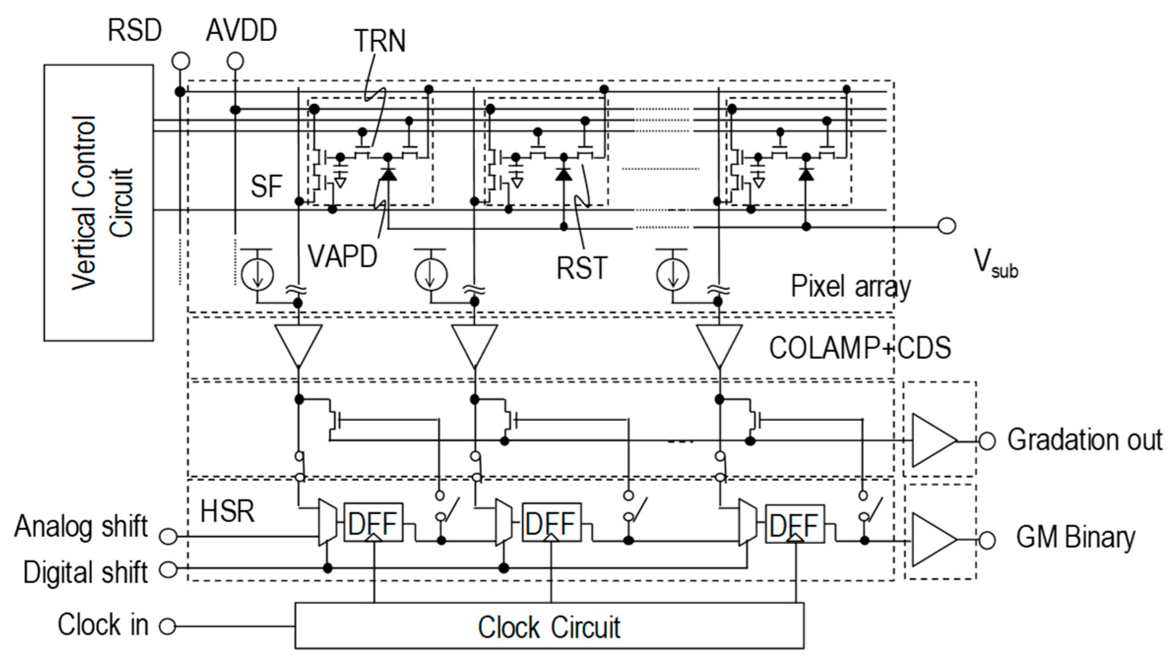
| CMOS Technology | 65 nm 1P4M |
|---|---|
| Pixel Size | 6 µm |
| Array size | 400 × 400 |
| Physical Signal | Photo-Charge |
| Quenching Type | Capacitive quenching |
| Fill Factor | 70% |
| Operation Voltage | −3.3 V~−29 V |
| DCR(@RT) | 100 cps |
| Frame Rate | 60 fps |
© 2020 by the authors. Licensee MDPI, Basel, Switzerland. This article is an open access article distributed under the terms and conditions of the Creative Commons Attribution (CC BY) license (http://creativecommons.org/licenses/by/4.0/).
Share and Cite
Inoue, A.; Okino, T.; Koyama, S.; Hirose, Y. Modeling and Analysis of Capacitive Relaxation Quenching in a Single Photon Avalanche Diode (SPAD) Applied to a CMOS Image Sensor. Sensors 2020, 20, 3007. https://doi.org/10.3390/s20103007
Inoue A, Okino T, Koyama S, Hirose Y. Modeling and Analysis of Capacitive Relaxation Quenching in a Single Photon Avalanche Diode (SPAD) Applied to a CMOS Image Sensor. Sensors. 2020; 20(10):3007. https://doi.org/10.3390/s20103007
Chicago/Turabian StyleInoue, Akito, Toru Okino, Shinzo Koyama, and Yutaka Hirose. 2020. "Modeling and Analysis of Capacitive Relaxation Quenching in a Single Photon Avalanche Diode (SPAD) Applied to a CMOS Image Sensor" Sensors 20, no. 10: 3007. https://doi.org/10.3390/s20103007