Remote Control System for Battery-Assisted Devices with 16 nW Standby Consumption


Abstract
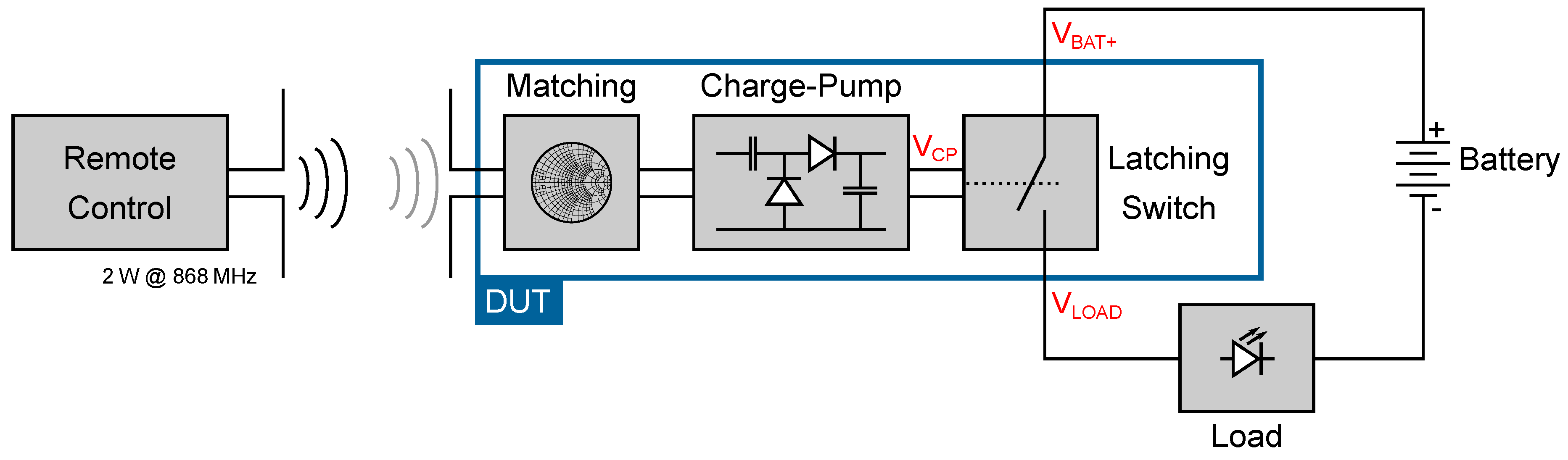
:1. Introduction
- Remote Control (RC): To switch a device ‘on’ and ‘off’ via the air interface, a remote control can be used which wakes the device up from standby or switches it to standby. An example for this method is the infrared RC in TV’s or DVD players. However, devices in standby must scan the environment for switch-on signals, which leads to a non-negligible power consumption. Although the European Union’s ‘Ecodesign Directive (2009/125/EC)’ has limited the tolerable standby consumption to in 2013, it is still too high, considering the sheer number of IoT devices.
- Target Time: With this option, the node that is in standby mode decides itself when to wake up. Afterwards, it sends a signal to the network to indicate its ‘on’ and then remains in receive mode before returning to standby after a certain time. The internal wake-up logic requires little resources, resulting in a nearly ‘Zero-Watt’ standby mode. However, this method also has disadvantages. The device cannot be woken up by an external device such as a remote control and is therefore limited to fixed time slots. Furthermore, the node is woken up even if it is not necessary, which leads to additional energy consumption. This method is used in LTE-M, which is specified for IoT [4].
2. Implementation
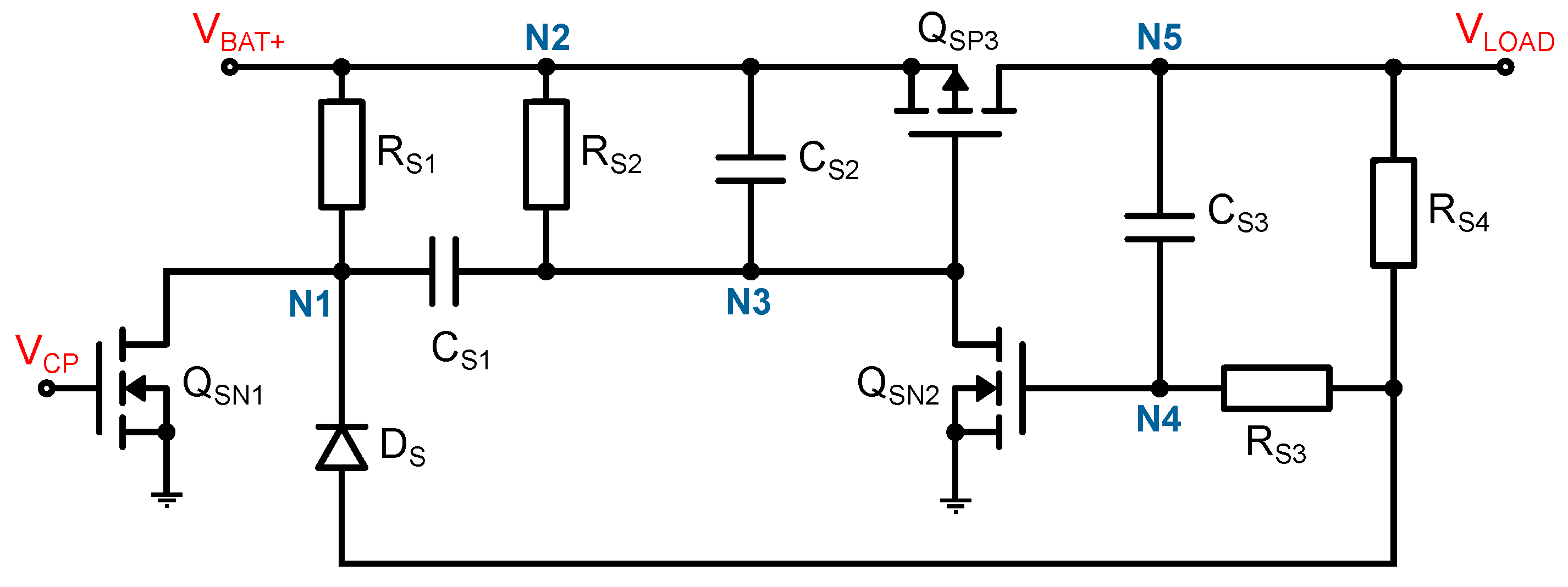
2.1. Latching Switch
- Initial State: When no AC signal is applied to the CP, is floating and therefore no gate-source-voltage is applied to . When the battery gets connected (), the capacitor shorts node N3 with at first and thus determines the standard starting state. This prevents a floating node, which would inadvertently switch on . The potential of the nodes N1, N2 and N3 is . Therefore, the PMOS (P-type metal-oxide-semiconductor) transistor blocks and the potential of node N5 will be pulled to ground (GND) via the load. Thus, N4 is also on the same potential and the gate of will not be connected to GND over . The off state will be kept and is on the same potential as GND.
- Switching ON: When a voltage is applied to , it pulls the node N1 to GND. In the first moment, the capacitor acts as a short and thus N3 will also become GND which allows to connect. The potential of N5 is applied to N4 via which causes to connect through and pull the gate of permanently to GND. Even if again, the on state will be kept and .
- Switching OFF: When a voltage is applied to , it pulls the node N1 to GND. The capacitor will be charged via the diode and pulls N4 towards GND. When the potential at N4 is falling below the threshold voltage of , it stops connecting through and the gate of will be high again. The battery is disconnected from the load and the off state will be kept.
2.2. Charge Pump
2.3. Matching Network and Antenna
- Input Power for Matching: Since the input impedance of the circuit depends on the input power, this must be determined in the first step. A common approach is presented in [23]. First, the unmatched circuit is connected to a digital signal generator (DSG) via cable (Sucoflex 104, ) to get the minimum needed power to control the actuator. This power is used as output power at the vector network analyzer (VNA) to determine the corresponding . The calculated sensitivity of the actuator is then derived from [23]
- Actuator Impedance Determination: The input impedance of the actuator circuit for has been determined with a network analyzer and results in:
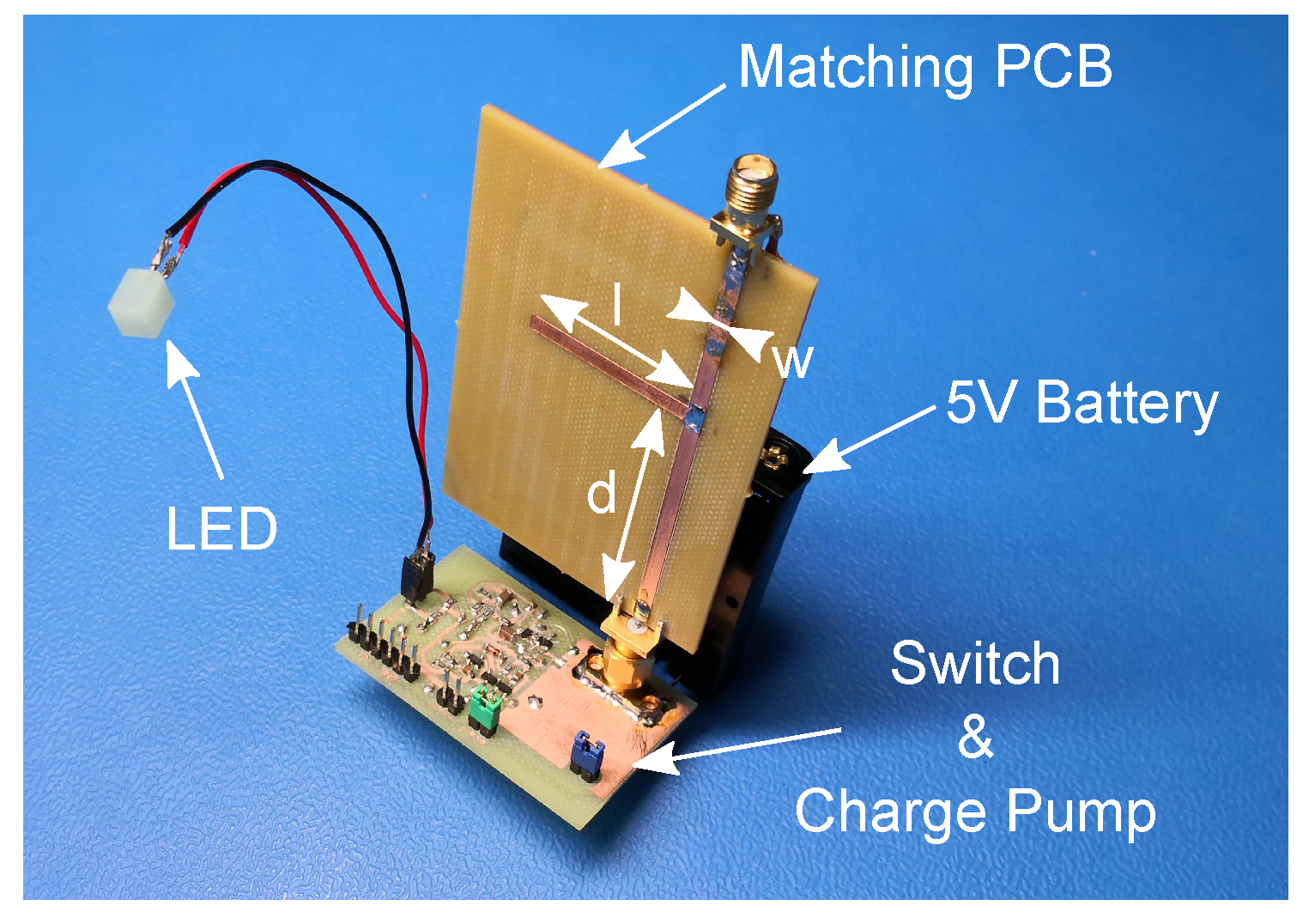
- Matching Network Calculation: Due to the high frequency, a single microstrip stub tuner is used for the matching of the actuator impedance with . The geometry of the matching can be seen in Figure 4. The two dimensioning parameters d and l can be calculated according to [24] and lead to:The effective wavelength depends on the PCB material and the microstrip width w. For the calculations, the ‘PCB Toolkit’ from ‘Saturn PCB Design’ has been used. To achieve a Ω wave impedance on our ‘Panasonic R-1566 FR4’ [25] laminate for MHz, the width w needs to be . Therefore, the effective wavelength and this results in the final parameters:
- Fabrication: The circuit was fabricated on the selected laminate and SMA connectors were mounted on the PCB (see Figure 4).
- Verification: For verification, the actuator and the matching network were connected to the network analyzer. The results show there is a good agreement between calculation, simulation and measurement. An impedance of has been measured, which indicates a proper matching.
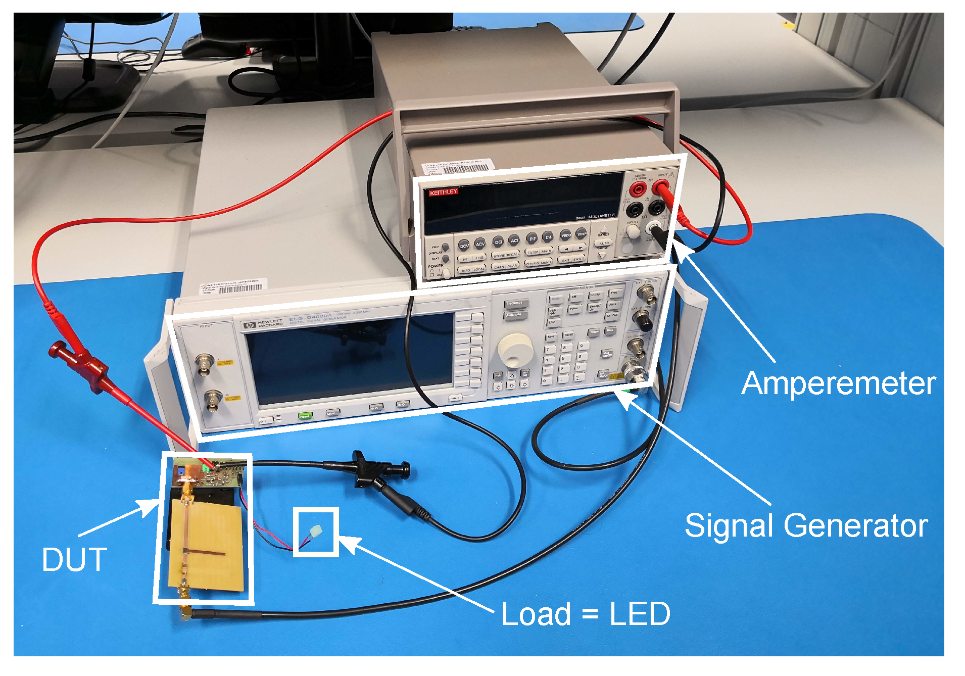
2.4. Device under Test
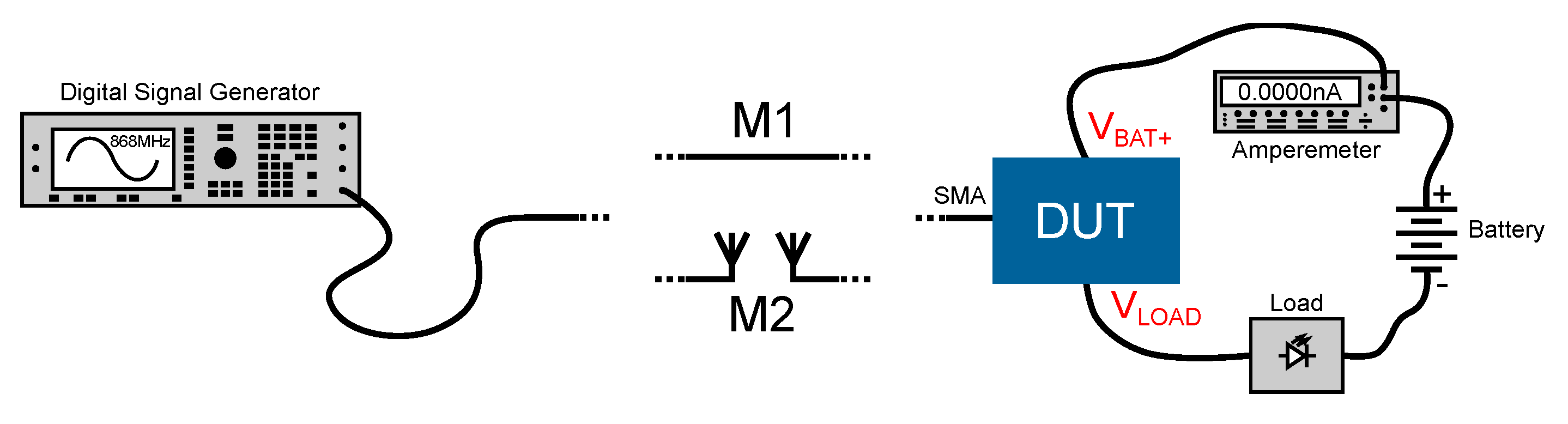
3. Measurement Setup
4. Results
4.1. Wired (M1)
4.2. Wireless (M2)
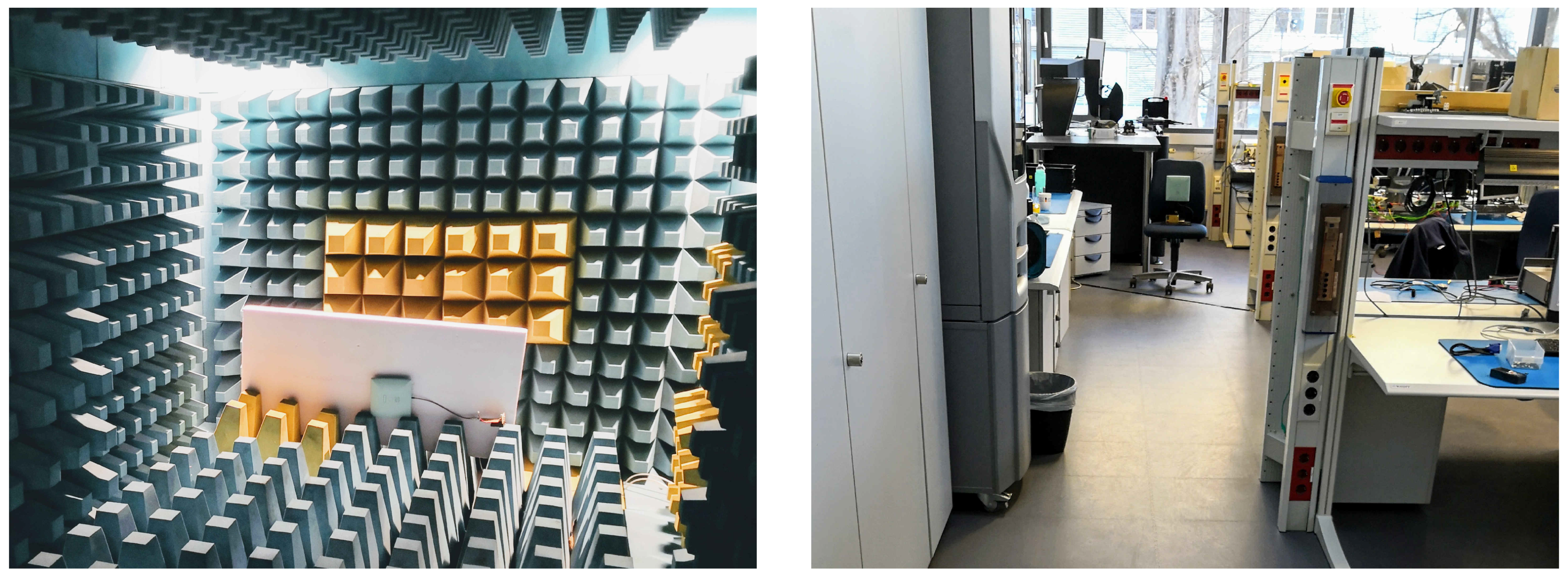
4.2.1. Anechoic Chamber Measurement
4.2.2. Multipath Environment Measurement
| max. allowed ERP | ||
| + | isotropic gain of a half-wave dipole | |
| = | max. allowed EIRP (effective isotropic radiated power) | |
| − | RF660A antenna gain | |
| + | cable attenuation | |
| = | DSG output power. |
5. Conclusions
Author Contributions
Funding
Conflicts of Interest
References
- Prauzek, M.; Konecny, J.; Borova, M.; Janosova, K.; Hlavica, J.; Musilek, P. Energy harvesting sources, storage devices and system topologies for environmental wireless sensor networks: A review. Sensors 2018, 18, 2446. [Google Scholar] [CrossRef] [PubMed]
- Ferdik, M.; Saxl, G.; Gunjic, D.; Ussmueller, T. Spectral efficiency increase for passive backscatter communication based on discrete pulse shaping. IEEE Access 2018, 6, 50875–50881. [Google Scholar] [CrossRef]
- Hagelauer, A.; Ussmueller, T.; Weigel, R. SAW and CMOS RFID transponder-based wireless systems and their applications. In Proceedings of the IEEE International Frequency Control Symposium, Baltimore, MD, USA, 21–24 May 2012. [Google Scholar]
- Liberg, O.; Sundberg, M.; Wang, E.; Bergman, J.; Sachs, J. Cellular Internet of Things: Technologies, Standards, and Performance; Academic Press: London, UK, 2018; pp. 21–24. [Google Scholar]
- Yi, K.H. Cost-effective power system design reducing standby power consumption for the consumer electronic devices. In Proceedings of the IEEE Applied Power Electronics Conference and Exposition, Long Beach, CA, USA, 17–21 March 2013. [Google Scholar]
- Boaventura, A.J.S.; Carvalho, N.B. A battery-less remote control based on a novel multi-RFID scheme. In Proceedings of the European Microwave Conference, Nuremberg, Germany, 6–10 October 2013. [Google Scholar]
- Boaventura, A.J.S.; Carvalho, N.B. A batteryless RFID remote control system. IEEE Trans. Microw. Theory Tech. 2013, 61, 2727–2736. [Google Scholar] [CrossRef]
- Zhang, L.; Jiang, H.; Sun, X.; Zhang, C.; Wang, Z. A passive RF receiving and power switch ASIC for remote power control with zero stand-by power. In Proceedings of the IEEE Asian Solid-State Circuits Conference, Fukuoka, Japan, 3–5 November 2008. [Google Scholar]
- Chen, L.; Wang, Z.; Jia, C.; Li, F.; Hao, W.; Xiao, B.; Zhang, C.; Wang, Z. A RF remote-control transceiver with zero-standby power based on RFID technology. In Proceedings of the Asia Pacific Conference on Postgraduate Research in Microelectronics and Electronics, Shanghai, China, 22–24 September 2010. [Google Scholar]
- Kang, S.; Park, K.; Shin, S.; Chang, K.; Kim, H. Zero standby power remote control system using light power transmission. IEEE Trans. Consum. Electron. 2011, 57, 1622–1627. [Google Scholar] [CrossRef]
- Yamawaki, A.; Serikawa, S. An extending method of operable distance for infrared remote controlled power switch with zero stand-by power. In Proceedings of the International Conference on Informatics, Electronics & Vision, Fukuoka, Japan, 15–18 June 2015. [Google Scholar]
- Goyal, D. Sonal, Power management in Wireless Sensor Network. In Proceedings of the 3rd International Conference on Computing for Sustainable Global Development, New Delhi, India, 16–18 March 2016. [Google Scholar]
- Munir, B.; Dyo, V. On the Impact of mobility on battery-less RF energy harvesting system performance. Sensors 2018, 18, 3597. [Google Scholar] [CrossRef] [PubMed]
- Ju, Q.; Zhang, Y. Predictive power management for internet of battery-less things. IEEE Trans. Power Electron. 2018, 33, 299–312. [Google Scholar] [CrossRef]
- Yang, S.; Yang, X.; McCann, J.A.; Zhang, T.; Liu, G.; Lio, Z. Distributed networking in autonomic solar powered wireless sensor networks. IEEE J. Sel. Areas Commun. 2013, 31, 750–761. [Google Scholar] [CrossRef]
- Gorlatova, M.; Wallwater, A.; Zussman, G. Networking low-power energy harvesting devices: Measurements and algorithms. IEEE Trans. Mob. Comput. 2013, 12, 1853–1865. [Google Scholar] [CrossRef]
- Pizzotti, M.; Perilli, L.; Del Prete, M.; Fabbri, D.; Canegallo, R.; Dini, M.; Masotti, D.; Costanzo, A.; Franchi Scarselli, E.; Romani, A. A long-distance RF-powered sensor node with adaptive power management for IoT applications. Sensors 2017, 17, 1732. [Google Scholar] [CrossRef] [PubMed]
- Yildiz, H.U.; Gungor, V.C.; Tavli, B. A hybrid energy harvesting framework for energy efficiency in wireless sensor networks based smart grid applications. In Proceedings of the 17th Annual Mediterranean Ad Hoc Networking Workshop, Capri, Italy, 20–22 June 2018. [Google Scholar]
- Ferdik, M.; Saxl, G.; Ussmueller, T. Battery-less UHF RFID controlled transistor switch for Internet of Things applications—A feasibility study. In Proceedings of the IEEE Topical Conference on Wireless Sensors and Sensor Networks, Anaheim, CA, USA, 14–17 January 2018. [Google Scholar]
- GS1 EPCglobal Inc. EPC Radio-Frequency Identity Protocols Generation-2 UHF RFID, V2. Available online: https://www.gs1.org/sites/default/files/docs/epc/uhfc1g2_2_0_0_standard_20131101.pdf (accessed on 1 November 2013).
- Mosaic Documentation Web—Latch and Toggle Power Circuits. Available online: www.mosaic-industries.com/embedded-systems/microcontroller-projects/electronic-circuits/push-button-switch-turn-on/latching-toggle-power-switch (accessed on 1 February 2019).
- EEVBlog—Word’s Simplest Soft Latching Power Switch Circuit. Available online: www.eevblog.com/2012/03/30/eevblog-262-worlds-simplest-soft-latching-power-switch-circuit/ (accessed on 1 February 2019).
- Nikitin, P.V.; Seshagiri Rao, K.V.; Martinez, R.; Lam, S.F. Sensitivity and Impedance Measurements of UHF RFID Chips. IEEE Trans. Microw. Theory Tech. 2009, 57, 1297–1302. [Google Scholar] [CrossRef] [Green Version]
- All About Circuits—Learn Stub Tuning with a Smith Chart. Available online: https://www.allaboutcircuits.com/technical-articles/learn-stub-tuning-with-a-smith-chart/ (accessed on 4 February 2019).
- R-1566 Laminate. Available online: https://industrial.panasonic.com/content/data/EM/PDF/ipcdatasheet_1707_R-1566(W_WN).pdf (accessed on 9 January 2019).
- Friis, H.T. A note on a simple transmission formula. Proc. IRE 1946, 34, 254–256. [Google Scholar] [CrossRef]
- European Radiocommunications Committee (ERC), ERC Recommendation 70-03—Relating to the use of Short Range Devices (SRD). Available online: https://www.ecodocdb.dk/download/25c41779-cd6e/Rec7003.pdf (accessed on 5 October 2018).


| Component | Type | Component | Type |
|---|---|---|---|
| BSH105 | |||
| , | BSS138 | ||
| BSS84 | |||
| 1 F | |||
| 2.2 F | , | HSMS285 | |
| 1N4148 | Zener |
© 2019 by the authors. Licensee MDPI, Basel, Switzerland. This article is an open access article distributed under the terms and conditions of the Creative Commons Attribution (CC BY) license (http://creativecommons.org/licenses/by/4.0/).
Share and Cite
Ferdik, M.; Saxl, G.; Jesacher, E.; Ussmueller, T. Remote Control System for Battery-Assisted Devices with 16 nW Standby Consumption. Sensors 2019, 19, 975. https://doi.org/10.3390/s19040975
Ferdik M, Saxl G, Jesacher E, Ussmueller T. Remote Control System for Battery-Assisted Devices with 16 nW Standby Consumption. Sensors. 2019; 19(4):975. https://doi.org/10.3390/s19040975
Chicago/Turabian StyleFerdik, Manuel, Georg Saxl, Erwin Jesacher, and Thomas Ussmueller. 2019. "Remote Control System for Battery-Assisted Devices with 16 nW Standby Consumption" Sensors 19, no. 4: 975. https://doi.org/10.3390/s19040975