1. Introduction
Voltage/electric field sensors are widely used in a variety of applications such as power grids [
1], Internet of Things (IoT) [
2], oil well health monitoring [
3], and even smart houses [
4]. Traditional voltage measuring devices include resistance voltage dividers, capacitive voltage dividers, and electromagnetic voltage transformers. Capacitive dividers and electromagnetic voltage transformers are usually used for AC voltage measurement. Resistance voltage dividers can be used for either DC or AC voltage measurement [
5]. However, the self-heating effect of resistances causes additional power consumption and inaccuracy problems.
The past few decades has witnessed the development of many novel DC/AC voltage sensors such as the optical voltage sensors (OVSs) based on a linear electro-optic effect (Pockels effect) [
6], and Kerr effect [
7]. In addition, the voltage sensors using piezoelectric material (Pb(Zr
1−xTi
x)O
3, PZT) as a voltage transducer and a fiber Bragg grating as a strain sensor have also been developed [
8]. The voltage sensors employ electro-optical crystal or piezoelectric material and feature high input resistance of a few hundred GΩ, a small size, low weight, and immunity to electromagnetic interference. However, these OVSs need complicated photoelectric demodulation systems where measurement accuracy is easily influenced by light intensity and temperature. Xue et al. [
9] reported a piezoelectric–piezoresistive coupling MEMS sensor, which could be used to measure a DC/AC electric field or voltage with a broadened frequency bandwidth of up to 100 kHz. Sasaki et al. [
10,
11] reported a MEMS resonator-based voltage sensor in which the resonator was designed as a floating electrode sandwiched between a high-voltage electrode and a driving electrode. The transverse electrostatic attraction force generated by the electrical field of a high DC voltage source draws the frequency change of the resonator. However, the sensor shows strong nonlinearity over its measurement range of 400 V due to the nonlinear transverse electrostatic attraction force.
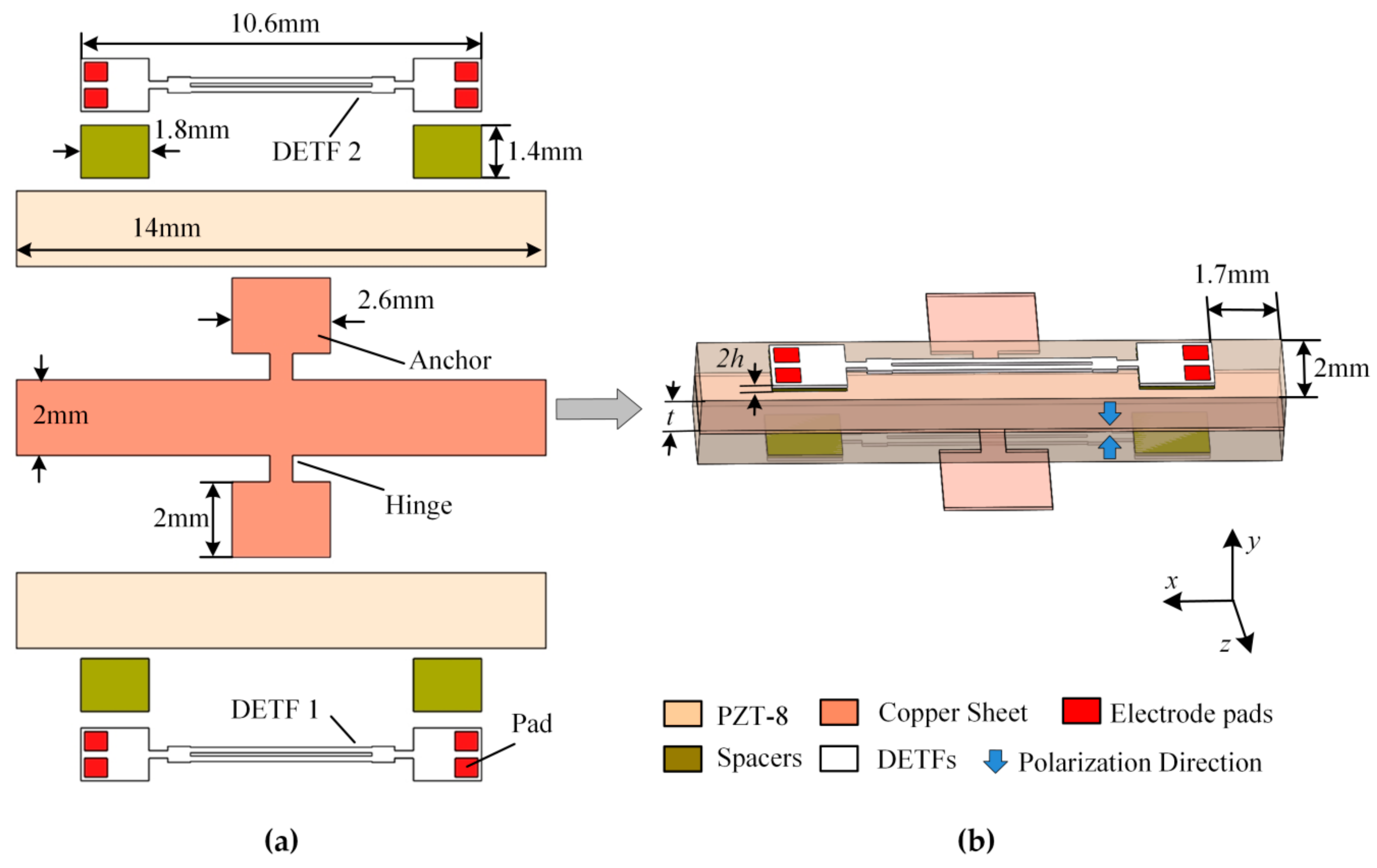
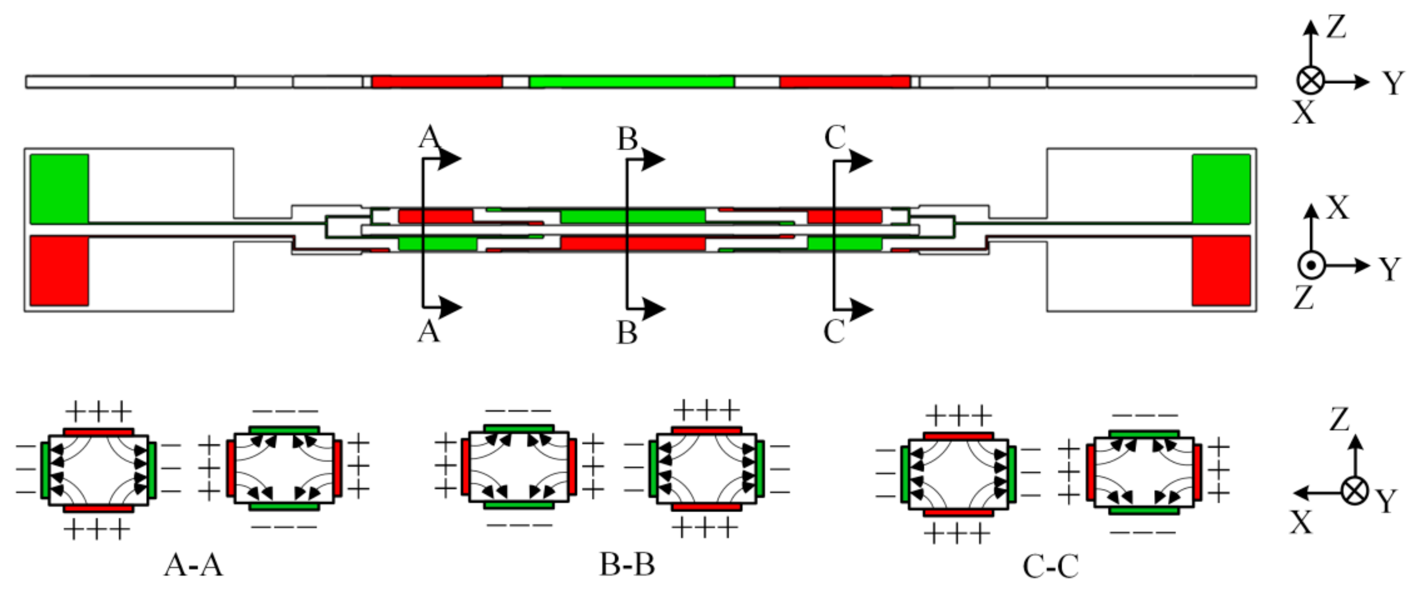
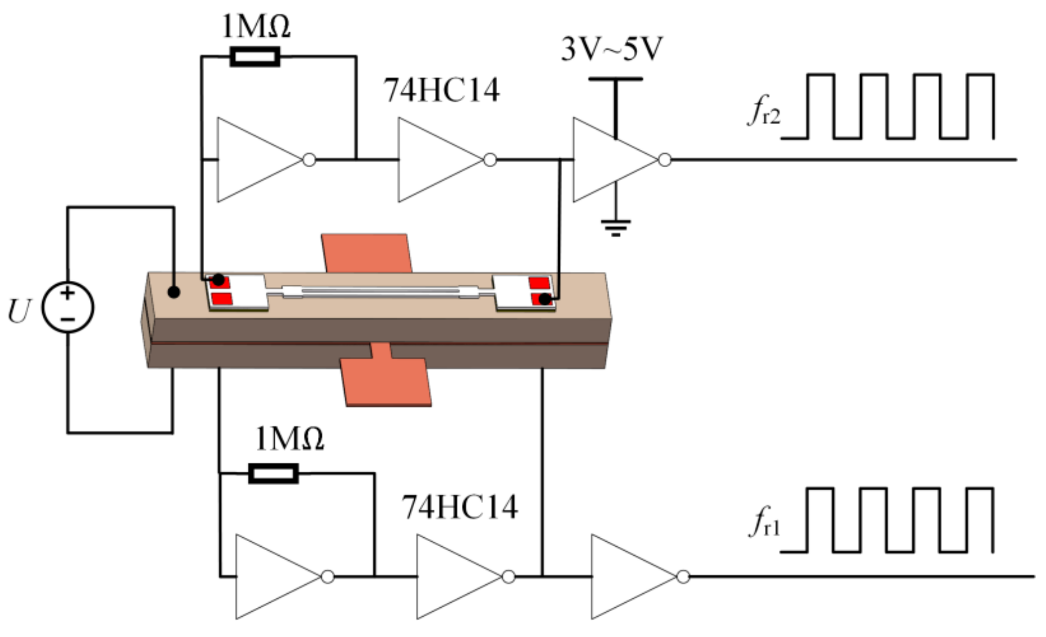
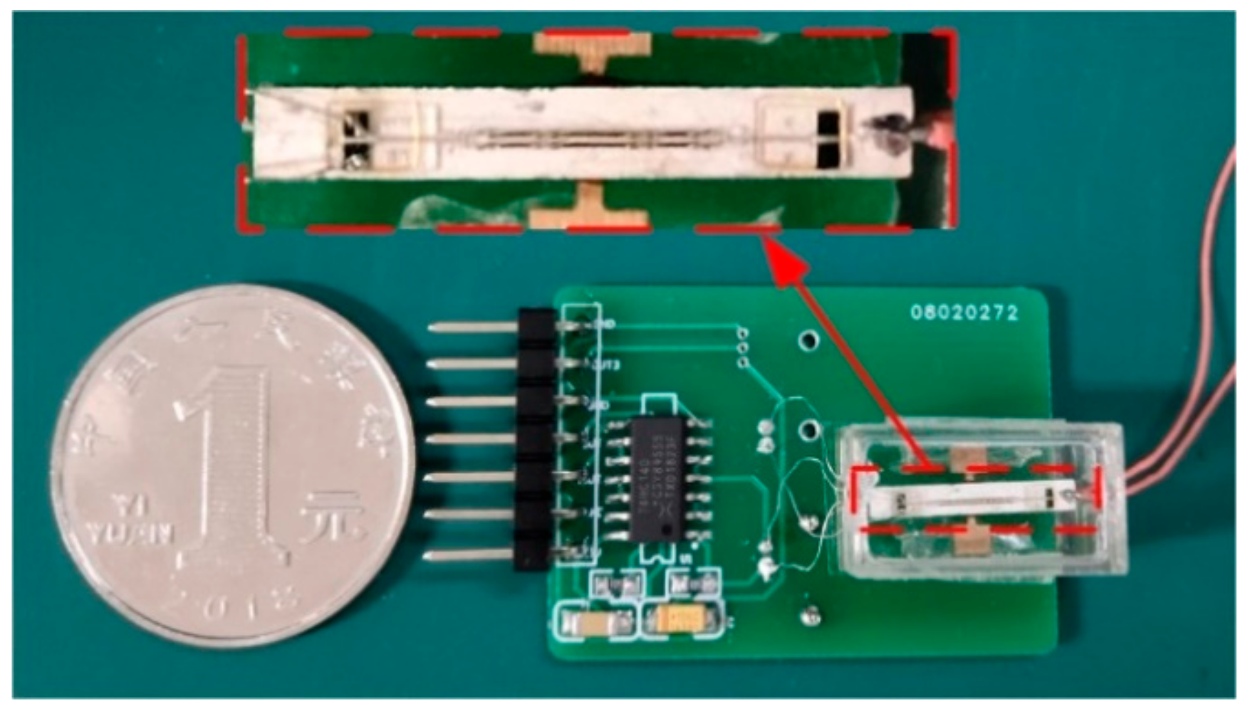
This paper reports on a differential resonant voltage sensor using a piezo bimorph as a voltage transducer and two differential quartz crystal double-ended tuning forks (DETFs) as force sensors. When a voltage is applied to the piezo bimorph, the tensile and compression deformations arise in the piezo bimorph due to the inverse piezoelectric effect and are transferred to the longitudinal of the dual DETFs whose resonant frequencies are in turn caused to increase and decrease, respectively. In the configuration, the differential output of the resonant frequencies of the dual DETFs doubled the sensor’s sensitivity and greatly reduced the influence of temperature drift. The frequency shift of the sensor can be measured by a frequency counter.
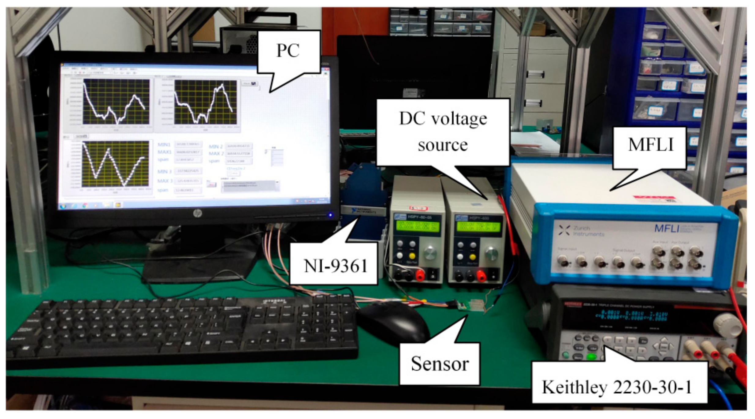
4. Results and Discussions
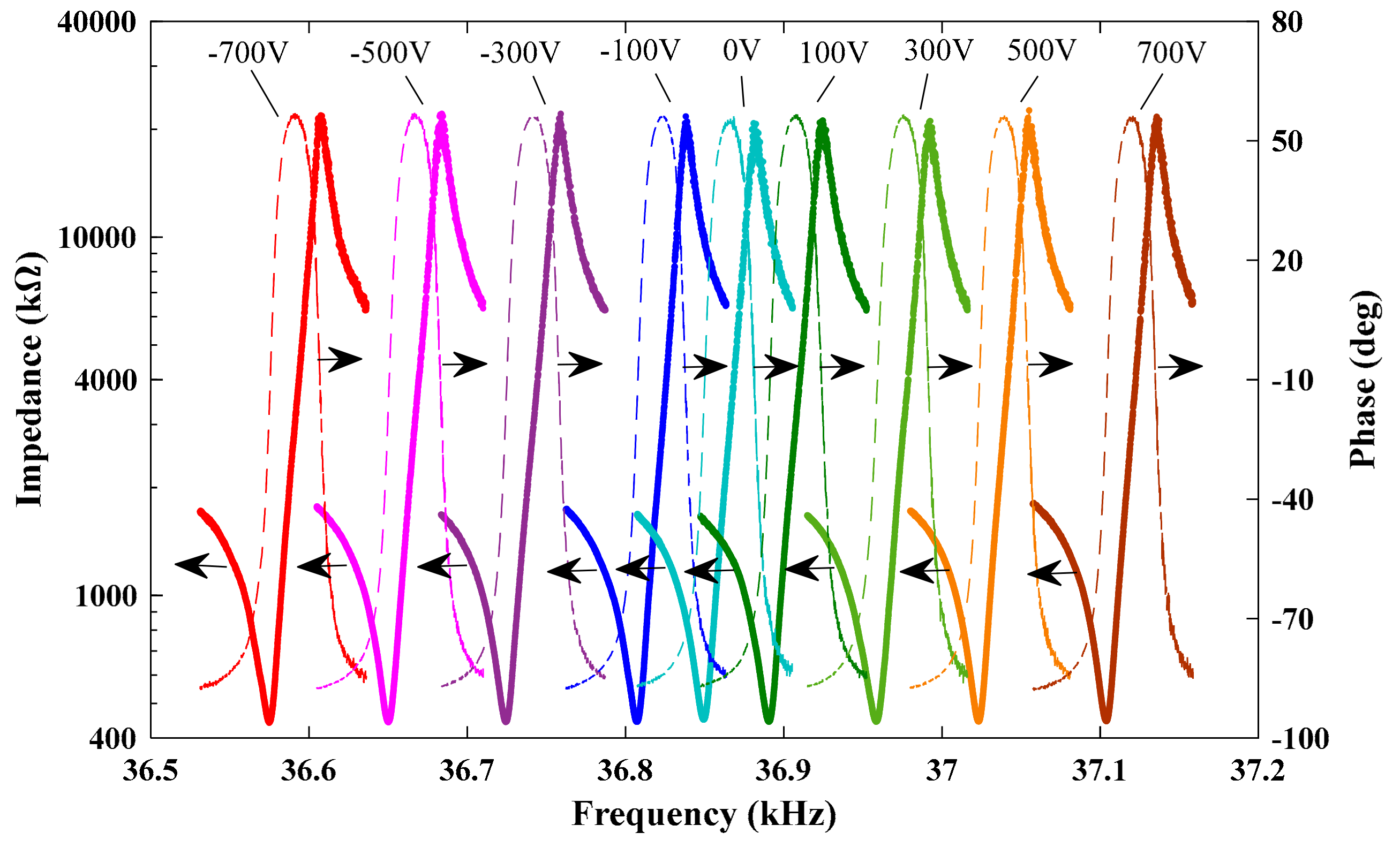
Figure 7 shows the impedance characteristics of the DETF 2. Obviously, the resonant frequencies clearly changed with the DC voltage. The
Q-factor of the DETF was determined by
, where,
was the resonant frequency of the DETF,
and
were the frequencies at the half power points. The values of
,
, and
were obtained from the impedance characteristics curves by the method described in [
17].
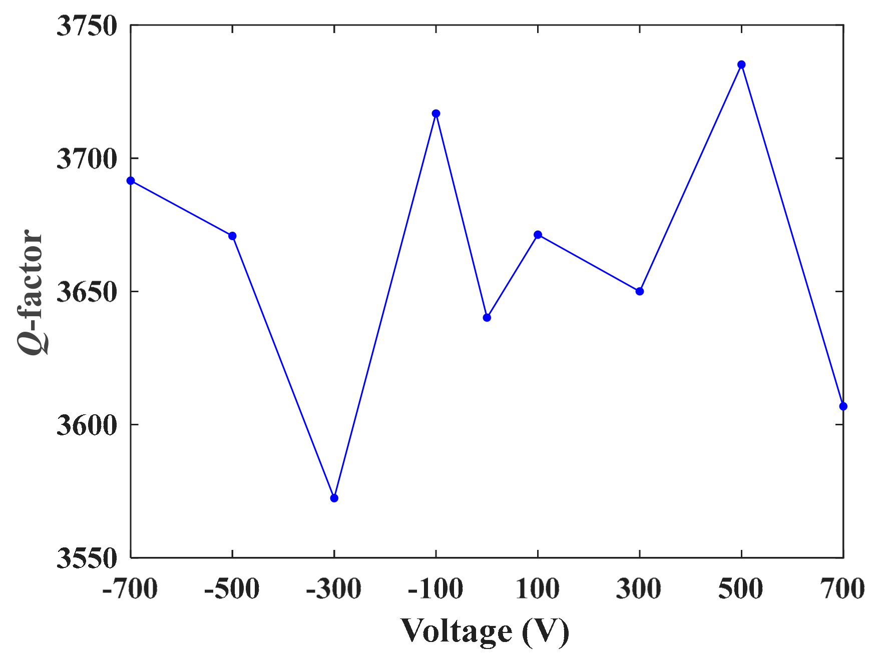
Figure 8 shows the
Q-factor of DETF 2 as a function of DC voltage. The
Q-factor fluctuated between 3572 and 3735, with an average value of 3661. The fluctuation of the
Q-factor may have resulted from the limited number of sweep data points of the impedance curves, which were measured by the sweep frequency method [
13]. The high
Q-factor meant that the sensor may have obtained high signal-to-noise ratio, high resolution and low power consumption.
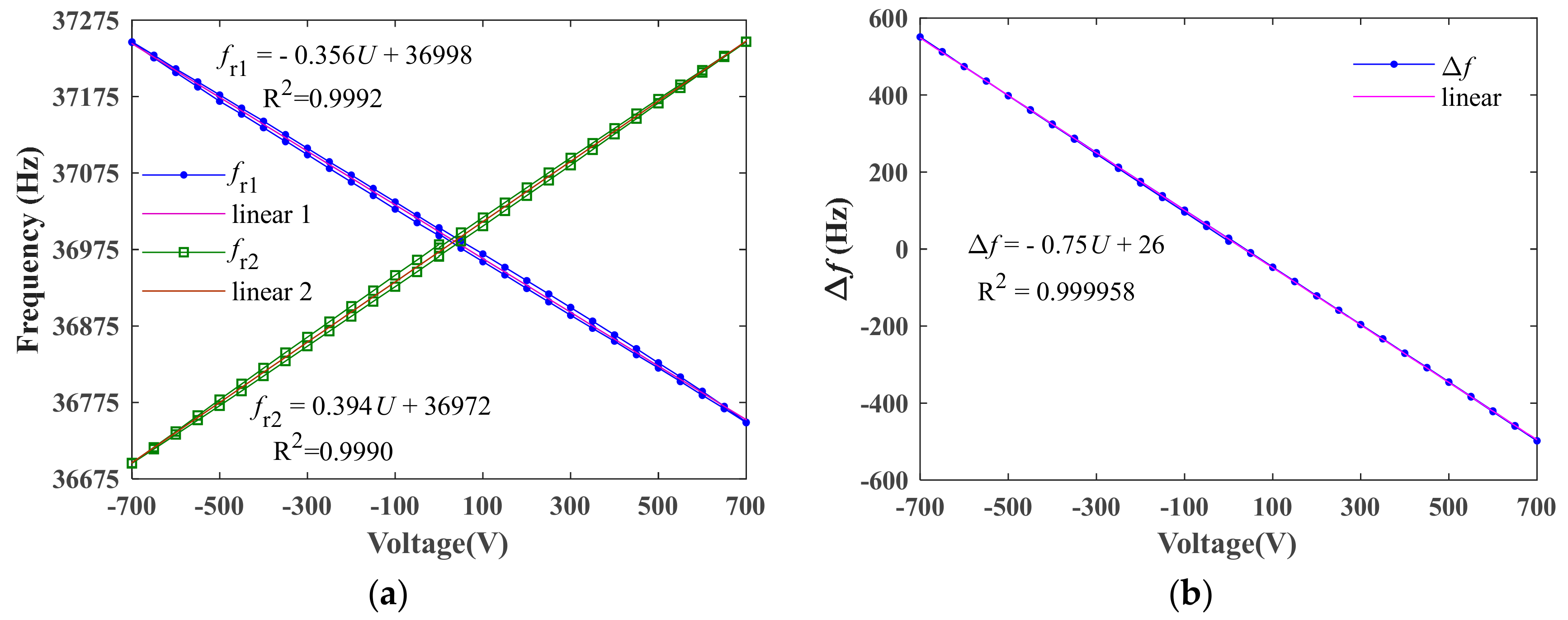
Figure 9a shows the resonant frequencies of DETF 1 and DETF 2 as a function of the applied DC voltage. In the range of ±700 V, the total frequency shift of DETF 1 and DETF 2 was 498 Hz and 551 Hz, respectively. The linear fitting functions were obtained as
(linear correlation coefficient R
2 = 0.9992) and
(linear correlation coefficient R
2 = 0.9990). Thus, the voltage sensitivities measured by DETF 1 and DETF 2 were 0.356 Hz/V and 0.394 Hz/V, respectively.
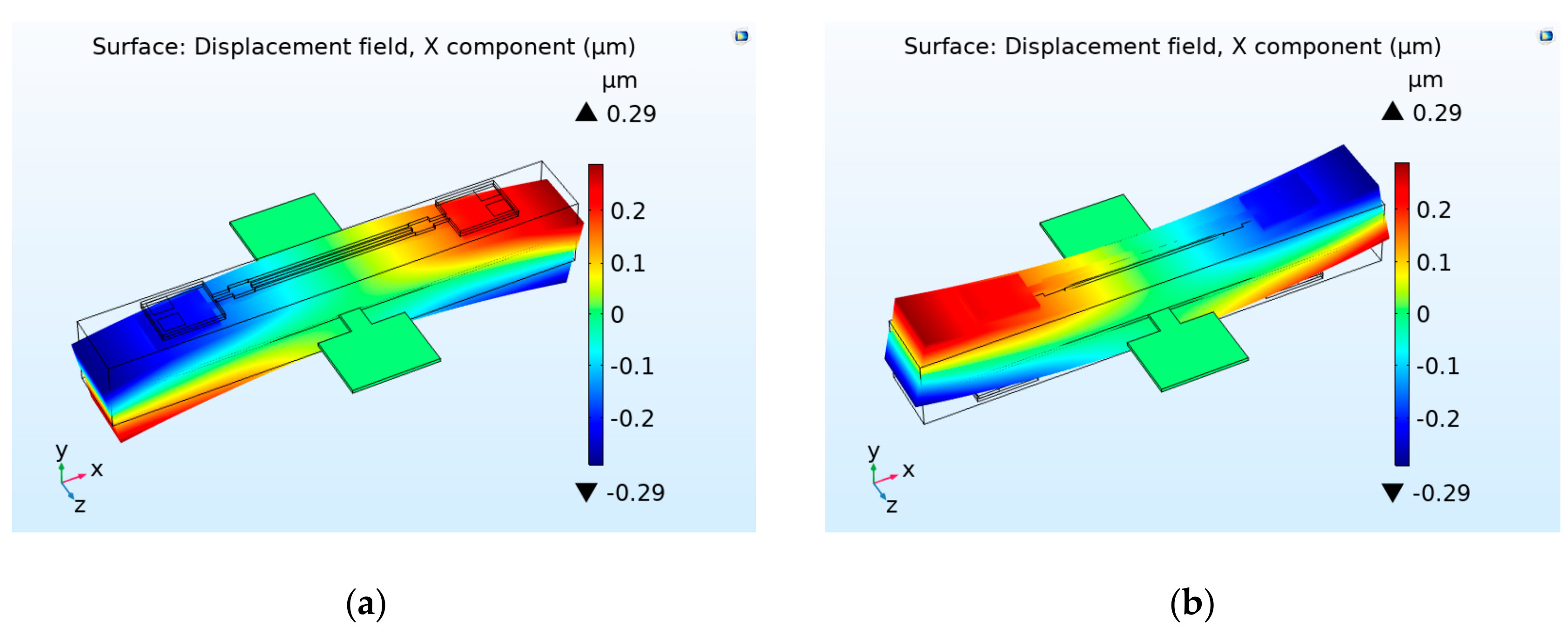
Figure 9b shows the differential frequency output of the sensor as a function of the applied DC voltage. In the differential configuration, the total frequency shift was almost doubled, being 1049 Hz. This result agreed well with the simulation result. The small difference between the experimental and simulation results may have resulted from the dimensions and parameters errors of the DETFs and the PZT-8 plates as well as the neglect of the adhesive layer in the simulation. From
Figure 9b, the linear fitting function became
(linear correlation coefficient R
2 = 0.999958) showing the sensitivity of the sensor as 0.75 Hz/V. In addition, the differential output of the sensor had a non-linearity error of 3 Hz (0.29% of the full range).
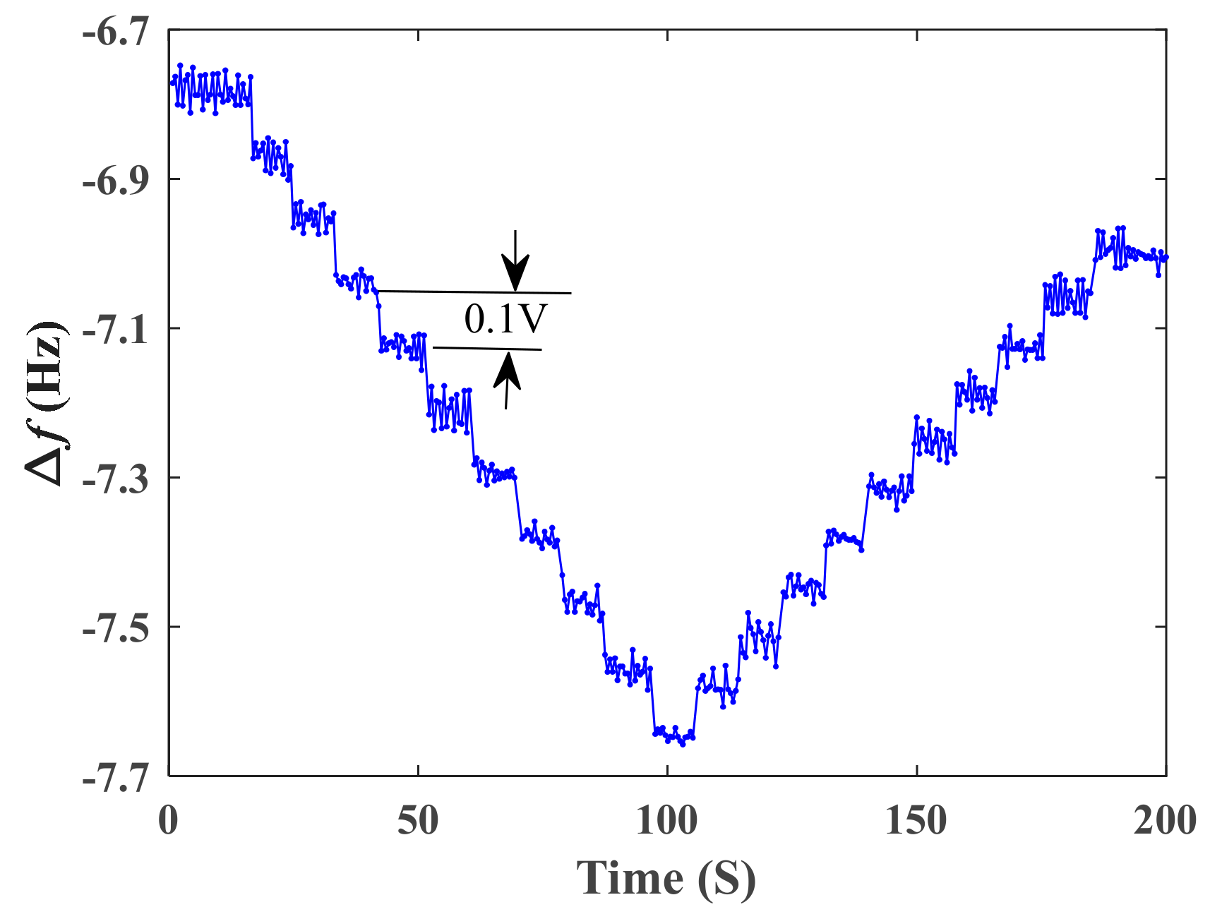
Figure 10 shows the response of the sensor to small step changes of DC voltage. The result shows that the differential frequency output of the sensor could distinguish the small step changes of DC voltage. The mean values of the differential frequency outputs
at the
voltage step and the step changes of the mean value
between the adjacent steps are show in
Table 3. There are 20 samples of the step changes. A two tail, one sample t-test at the 0.05 significance level (i.e.,
p-value ≤ 0.05) was used to check the resolution of the sensor. The mean value and standard deviation of
were calculated as 0.0756 Hz and 0.01156 Hz, respectively. Then the test statistic
t was calculated as
. With the assumption of a
p-value ≤ 0.05, one gets
. Then, the
p-value was calculated as 0.823 by using the t-test function in Matlab software, which was much larger than 0.05. It was shown that the resolution of the sensor could achieve 0.1 V (0.007% of the full range).
Figure 9 and
Figure 10 also show the behavior of the hysteresis loop when the DC voltage increased and then decreased. From
Figure 9, the maximum hysteresis of the differential frequency output was about 8 Hz (0.07% of the full range). For a voltage sensor employing piezoelectric material, the hysteresis effect is inevitable due to the time delay in domain switching [
18]. It is very important to reduce the hysteresis for sensing applications employing piezoelectric materials. Usually, the lag compensation methods which have been employed in many piezoelectric actuators can be taken to reduce the hysteresis [
19]. This work may be carried out in future.
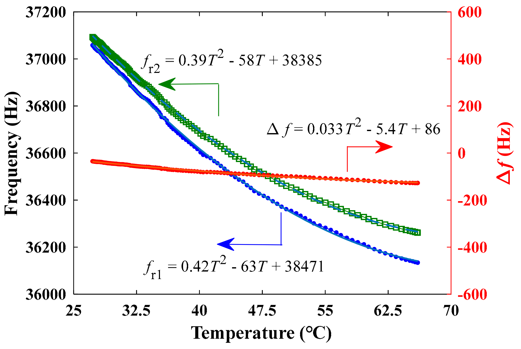
An initial evaluation of the temperature characteristics of the differential resonant voltage sensor was carried out.
Figure 11 shows the resonant frequencies of individual DETF and the differential frequency output as a function of temperature over room temperature of 27 °C to 67 °C. As can be seen, the resonant frequency shifts measured by the DETF 1 and DETF 2 were 925 Hz and 832 Hz over the temperature range from a room temperature of 27 °C to 67 °C, while the shift in the differential frequency output reduced to 93 Hz. Furthermore, by using the polynomial fitting method, one obtains the fitting function of the curves of
,
and
as follows:
where,
T is the temperature value. Then, the nonlinear temperature coefficients measured by the DETF 1 and DETF 2 were obtained as follows:
Where the nonlinear temperature sensitivity of the differential frequency output is as below:
From (11) to (13), the temperature coefficient in the differential mode was about an order smaller than that of the individual DETF. As the temperature changes, the induced stresses/strains in the piezoelectric and quartz materials by thermal expansion effect causes the resonant frequency of the dual DETFs to increase or decrease simultaneously. In this manner, the differential frequency output greatly reduces the influence of temperature drift. It is believed that the influence of the temperature drift can be further suppressed by the control of the fabrication process of sensors.
The main performance characteristics of the resonant voltage sensor is summarized in
Table 4. The piezo bimorph/quartz DETF-based resonant voltage sensor presented here was characterized by high linear characteristic over a wide measurement range, high sensitivity, excellent resolution, high input impedance and low-power requirements. Only a few hundred microwatts of power was needed to supply the oscillator circuit.


