Article

The Large-Scale Preparation and Optical Properties of MoS2/WS2 Vertical Hetero-Junction

Key Laboratory for Wide-Bandgap Semiconductor Materials and Devices of Education, the School of Microelectronics, Xidian University, Xi’an 710071, China
*
Authors to whom correspondence should be addressed.
Molecules 2020, 25(8), 1857; https://doi.org/10.3390/molecules25081857
Submission received: 14 March 2020 / Revised: 16 April 2020 / Accepted: 16 April 2020 / Published: 17 April 2020
(This article belongs to the Special Issue 25th Anniversary of Molecules—Recent Advances in Nanochemistry)

Abstract

:
A variety of hetero-junctions can be constructed to form the basic structural units in the different optoelectronic devices, such as the photo-detectors, solar cells, sensors and light-emitting diodes. In our research, the large-area high-quality MoS2/WS2 vertical hetero-junction are prepared by the two-step atmospheric pressure chemical vapor deposition (APCVD) methods and the dry transfer method, and the corresponding optimal reaction conditions of MoS2/WS2 vertical hetero-junction are obtained. The morphology, composition and optical properties of MoS2/WS2 vertical hetero-junction are systematically characterized by the optical microscopy, Raman spectroscopy, photoluminescence spectroscopy, atomic force microscopy and the field emission scanning electron microscopy. Compared to the mechanical transfer method, the MoS2/WS2 vertical hetero-junction sample obtained by the APCVD and dry transfer methods have lower impurity content, cleaner interfaces and tighter interlayer coupling. Besides, the strong interlayer coupling and effective interlayer charge transfer of MoS2/WS2 vertical hetero-junction are also further studied. The photoluminescence intensity of MoS2/WS2 vertical hetero-junction is significantly reduced compared to the single MoS2 or WS2 material. In general, this research can help to achieve the large-scale preparation of various Van der Waals hetero-junctions, which can lay the foundation for the new application of optoelectronic devices.

1. Introduction

The electronic chips integration increase with the development of modern semiconductor technology, and the volume of devices is becoming smaller, with the preparation processes becoming more complex [1,2,3]. The size of conventional Si-based CMOS devices has approached the limit, so researchers turn their attention to the two-dimensional transition metal dichalcogenides (2D TMDs) materials with single atomic layers. However, there are some limitations in the application of the single two-dimensional materials. The single h-BN material cannot be used in the devices alone, due to its wide band gap [4]. Additionally, the exposed BP is easily oxidized in the air, which would lead to the degradation of its performance [5]. As we all know, different two-dimensional materials have different energy band structures and band gaps. To further investigate the intrinsic properties of two dimensional materials and expand the application fields, the two dimensional hetero-junction materials can concentrate the advantages of two materials together to achieve the precise adjustment of the band gap, and it can also finely regulate the physical properties of the single materials. The advantage of Van der Waals (VDWs) atomic level hetero-junction has the convenience of modular combination, compared with the conventional hetero-junction. In other words, the atomic layer materials could be combined to prepare the hetero-junctions at will, which does not need to consider the lattice matching [6,7]. The corresponding hetero-junctions can be formed by stacking these atomic layer materials, which would show some properties not available in the single material. Besides, it can also achieve complementary properties.
The 2D TMD materials have large band gaps of a two-dimensional structure from the visible light to the near-infrared spectrum, adjustable carrier mobility, and electronic and optical characteristics related to the layer number [8,9]. It is these excellent characteristics that make them show great potential in the application of optoelectronic devices, such as the photo detectors [10], and the light emitting diodes [11]. The combination of MoS2 and WS2 films can effectively adjust the optical and electrical properties of MoS2/WS2 vertical hetero-junction through interlayer coupling, which would result in effective charge transfer and band structure reorganization. Meanwhile, they have a rich phenomenon of physics and electronics, which can also provide new opportunities for the design of novel electronic devices and photonic devices. In the previous reports, the mechanical stripping and chemical vapor deposition methods are usually used for the controlled and scalable production of the transition metal sulfides and the large-scale synthesis of TMDs with ideal architecture [12,13]. The mechanical exfoliation and directional transfer methods are the most widely used to study the VDWs hetero-structures, but the successful accumulation is accidental, and the methods have lower yield and efficiency [14]. Although some progress has been made in the preparation of TMD hetero-structures by the chemical vapor deposition method (CVD), conventional methods can usually only produce the lateral structures and not vertical hetero-structures. Therefore, there is still a huge challenge in using the existing exfoliation or CVD growth processes to achieve the scalable production of TMDs hetero-junctions with well-controlled structures.
The VDWs hetero-junction can be formed by using mechanical transfer technology to stack the different 2D materials, which has limited stacking orientation control. Compared to the mechanical transfer method, the direct growth of MX2 hetero-structure by CVD method not only has inherent scalability, but also has a cleaner interface and tighter interlayer coupling [15]. In this paper, the two-step atmospheric pressure chemical vapor deposition (APCVD) and dry transfer methods are used to epitaxially grow WS2 on MoS2, which can prepare the MoS2/WS2 vertical hetero-junction with its clean interface and strong interlayer coupling. The optimal processes’ reaction conditions of MoS2/WS2 vertical hetero-junction can also be obtained. Meanwhile, the morphology, composition and optical properties of MoS2/WS2 vertical hetero-junction are systematically characterized by optical microscopy, Raman spectroscopy, photoluminescence (PL) spectroscopy, atomic force microscopy, and field emission scanning electron microscopy. The results shown in this paper can provide effective guidance for future photonic devices, solar cells, photo-detectors, modulators, and storage devices [16].

2. The Introduction of Experiment

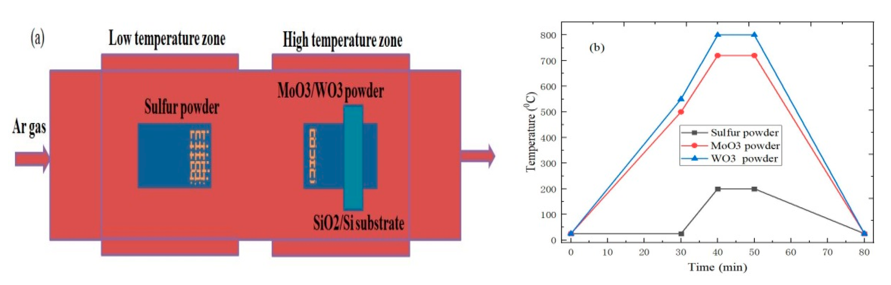
2.1. The Growth Experiments of MoS2 or WS2 by APCVD

The sulfur powder, tungsten trioxide, and molybdenum trioxide are respectively used as the sulfur source, tungsten source, and molybdenum source in the MoS2 or WS2 materials growth experiment, and the MoS2 and WS2 materials are respectively grown on SiO2/Si substrates by the atmospheric pressure chemical vapor deposition (APCVD) method. The following are the specific growth processes of single MoS2 or WS2 materials [17]. First, the SiO2/Si substrates are sequentially put into the absolute ethanol, acetone, and deionized water for 10 minutes, and then washed with the deionized water. Next, the first quartz boat with 0.1 g sulfur powder is put into the low temperature zone of the dual-temperature zone tube furnace. At the same time, the second quartz boat, equipped with 2 mg molybdenum source or tungsten source and the cleaned SiO2/Si substrate, is placed in the high temperature zone of the double temperature zone tube furnace, as shown in Figure 1a. Then, the tube furnace is evacuated to the vacuum state (1 Pa) when the vacuum pump is turned on, and then the high purity argon gas is used to fill the entire quartz tube chamber to reach the normal pressure state (100 KPa). The above operation is repeated three times to eliminate the air of the quartz tube. Subsequently, the heating program of the tube furnace is opened, and the growth temperatures of MoS2 and WS2 are respectively set to 720 °C and 800 °C due to the different sublimation points. The temperature of MoO3 powder increased from 25 °C to 720 °C, which was completed with a rate of 15.8 °C/min for 30 min and in turn 22 °C/min for 10 min. Meanwhile, the temperature of WO3 powder was increased from 25 °C to 800 °C, and successively heated at a rate of 17.5 °C/min for 30 min and 25 °C/min for 10 min. After the MoO3 and WO3 powders completed the first-stage heating, the temperature of sulfur powder increased from 25 °C to 200 °C in 10 min. Besides, the heating time remained unchanged for 10 min under the growth condition, and the flow rate of shielding gas is 35 sccm during the reaction. Finally, the heating program was turned off when the growth of single MoS2 or WS2 materials was completed, and the corresponding samples were taken out when the tube furnace was cooled to room temperature.

2.2. The Preparation Experiment of MoS2/WS2 Vertical Heterojunction

Meanwhile, the preparation processes of the MoS2/WS2 vertical hetero-junction by the dry transfer method are also described in previous work [18]. Based on the previous MoS2 and WS2 materials prepared by APCVD, the polymethyl methacrylate (PMMA) liquid was spin-coated on the WS2 at a speed of 4000 r/s, and annealed at 150 °C for 30 min. Additionally, the PMMA film can be immersed in the NaOH solution (Lingping Chemical Glass Instrument Co., Ltd., Guangzhou, China, 0.1 Mol/L). Then, the PMMA film with WS2 is floated and transferred to another SiO2/Si substrate, by using the transfer platform under the condition of CCD monitoring, which would overlap with the MoS2. Finally, the PMMA film is dissolved with acetone, and the MoS2/WS2 vertical hetero-junction can be obtained.

2.3. The Characterization of MoS2/WS2 Vertical Heterojunction

The Raman spectrum and PL spectrum of the MoS2/WS2 vertical hetero-junction are systematically analyzed by the LabRam HR Evolution Raman microscopy, equipped with the 532 nm laser under the 1mW laser power, and the laser spot size is 1μm. The high-resolution images can be obtained by using the 50× objective lens, 1800 lines/mm grating and the 500 nm imaging steps [19]. At the same time, the field emission scanning electron microscope (FESEM) and atomic force microscope (AFM) are also used to characterize the surface morphology and thickness of the MoS2/WS2 vertical hetero-junction.

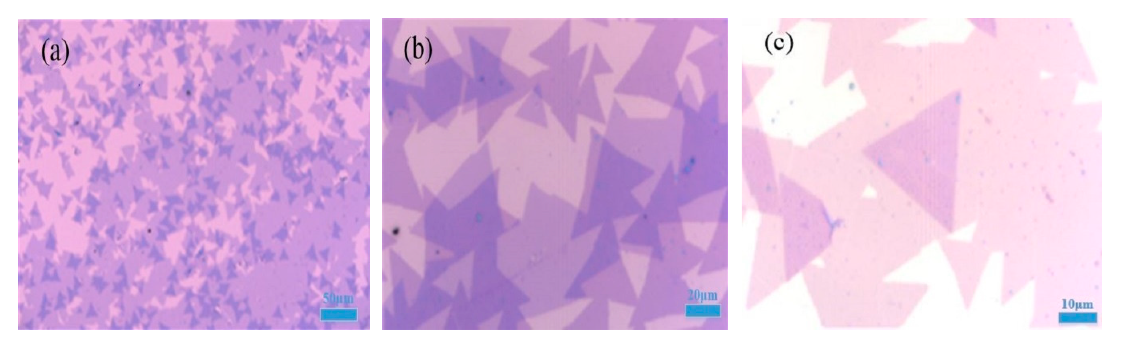
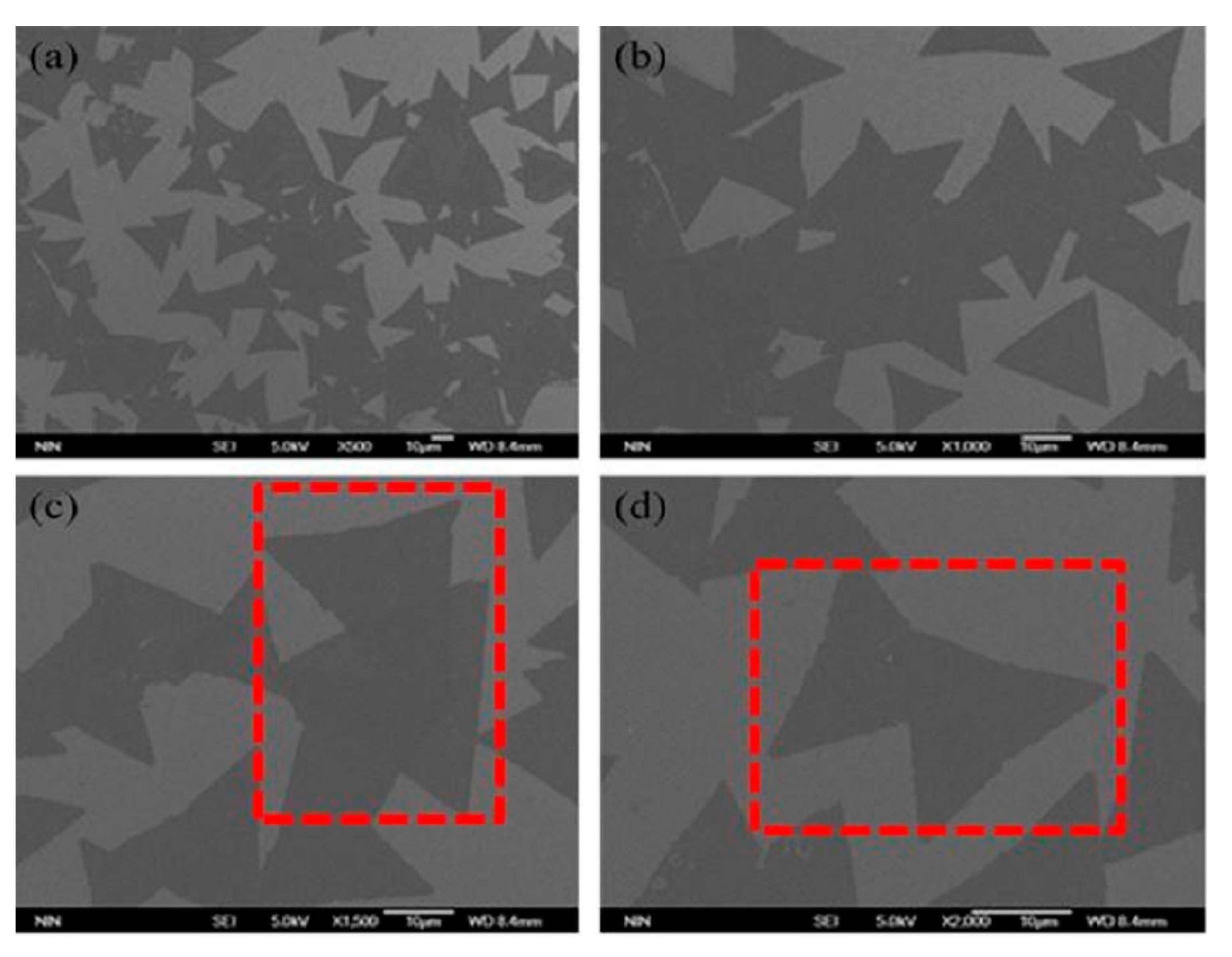
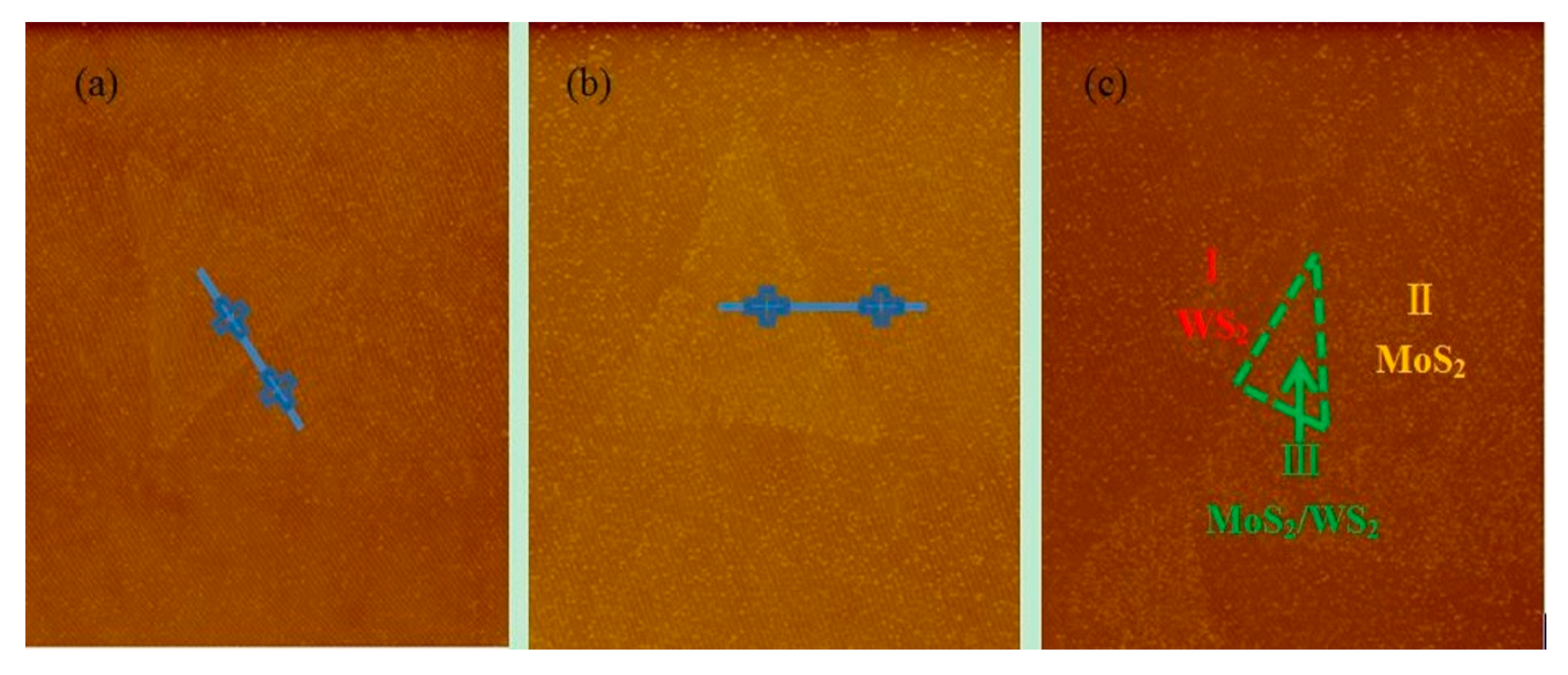
3. The Analysis of Characterization Results

In order to obtain better MoS2/WS2 vertical hetero-junction materials, we first need to grow the high-quality large-area single MoS2 or WS2 materials by APCVD. Under the optimal growth conditions, the gas concentration and nucleation density of single MoS2 or WS2 materials in the tube furnace can achieve the maximum values [20]. The MoS2/WS2 double-layer vertical hetero-junction can be prepared by the two-step APCVD method and the dry transfer processes. At the same time, the MoS2/WS2 vertical hetero-junction samples are systematically characterized by optical microscopy, Raman spectroscopy, PL spectroscopy, AFM and FESEM. In addition, the surface of WS2, MoS2, and MoS2/WS2 vertical hetero-junction samples are all uniform triangles with a size of several tens of microns after the corresponding growth reaction, and the color contrast between the samples and SiO2/Si substrate is relatively obvious, which can be distinguished by the optical microscope, as shown in Figure 2.
The MoS2/WS2 vertical hetero-junction on SiO2/Si substrate can also be observed by the FESEM. It can be found that the size of single WS2 or MoS2 materials are respectively 20 μm and 30 μm, and the contrast between single WS2 or MoS2 materials and SiO2/Si substrate is very uniform.
The reason the overlapping parts are not mixed together to form the WS2-MoS2 lateral hetero-junction is that we have adopted the two-step growth process. The first step is that the WoO3 powder forms the WS2 crystals during the high temperature (800 °C) reduction and vulcanization process, and the second step is that the MoO3 forms MoS2 crystals during the low temperature (720 °C) reduction and vulcanization process. Besides, the PMMA-assisted transfer method is used to transfer the monolayer WS2 to the monolayer MoS2 material, and the top WS2 layer has only 0° and 60° orientation relative to the bottom MoS2 layer in the red dotted box, which respectively correspond to A-A and A-B stacks [21,22], as shown in Figure 3. Therefore, unlike the traditional CVD method, the injection of Mo into Wo3 to form the lateral MoS2-WS2 mixture is effectively prevented.
Figure 4 shows the AFM images of MoS2, WS2, and MoS2/WS2 vertical hetero-junction. It can be found by observing the surface morphology and thickness that the thickness of the MoS2/WS2 vertical hetero-junction is about 1.7 nm, as shown in red mark region III. In order to further determine the thickness of single MoS2 and WS2 materials, the thickness of region II MoS2 and region I WS2 are respectively measured as 0.8 nm and 0.9 nm, which indicates the existence of monolayer WS2 and monolayer MoS2, and the lateral dimension is about 20–30 μm.

4. Introduction and Analysis of the Spectrum Characteristics

Raman spectrum and PL spectrum have become the effective way to detect and identify the optical properties and layer number of MoS2, WS2, and MoS2/WS2 vertical hetero-junction grown by the APCVD and dry transfer methods. The corresponding test characterizations require constant temperature and humidity, which are performed in an ultra-clean room environment.

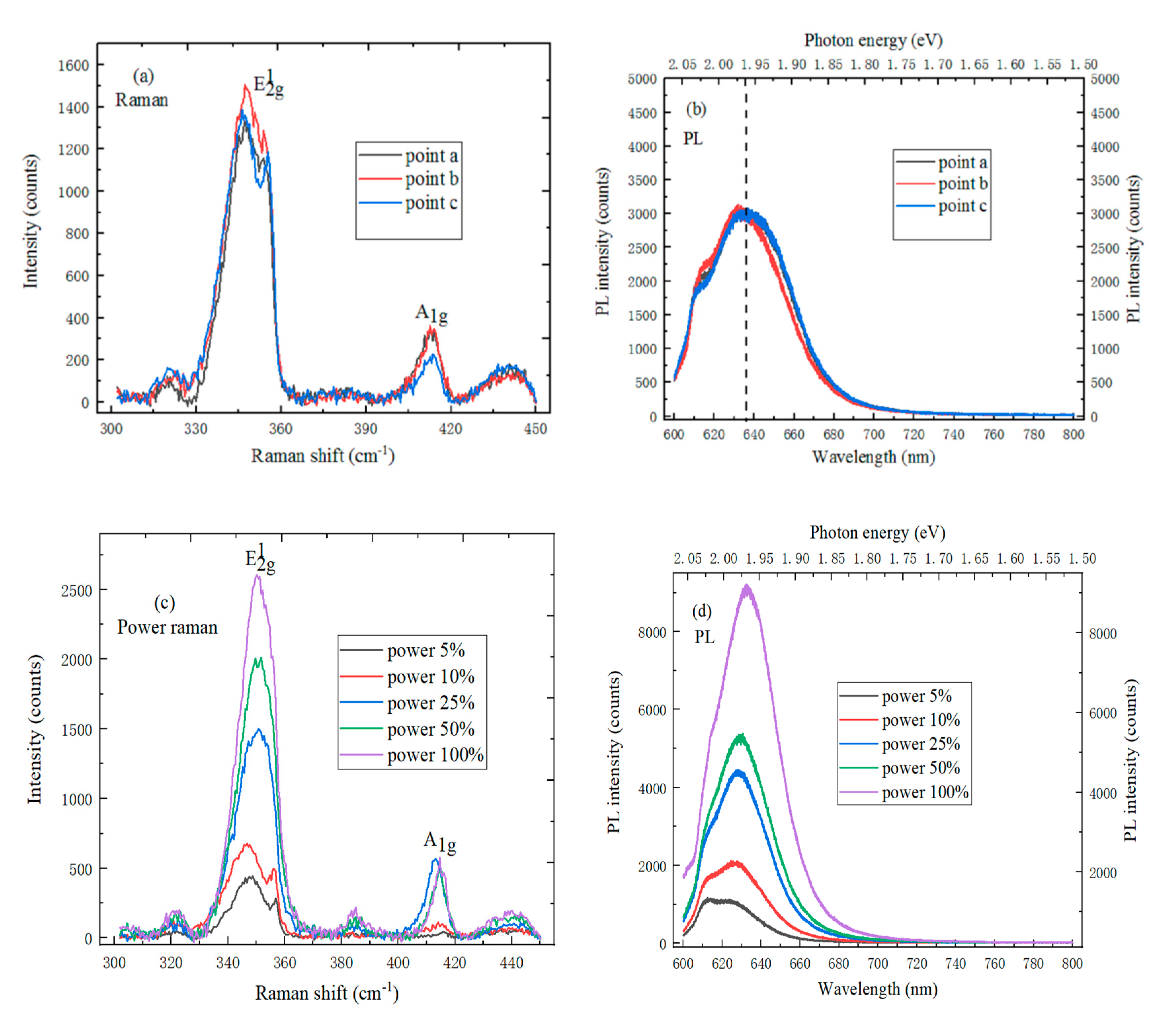
4.1. The Spectrum Characterization of Monolayer WS2

It can be found, by observing Figure 5a, that there are two characteristic peaks in the Raman spectrum of the WS2 sample, and the peak positions of the E12g and A1g characteristic peaks are respectively located at 349 cm−1 and 413 cm−1, which are fitted by the Gaussian function. The peak shift between two characteristic peaks decreases with the layer number decreases, which can be explained by the increase of the Van der Waals force. The Raman spectrums on the triangular WS2 sample remain consistent at different points, which can indicate that the sample is uniform. In Figure 5b, the strongest PL spectrum peak position of monolayer WS2 is located at 636 nm. The band gap of monolayer WS2 is calculated at 1.96 eV from the conversion relationship between the wavelength and electron volt, which is the same as the reported results. Besides, the PL spectrum also has an exciton peak of 2.04 eV. This is because the WS2 sample has energy band splitting [23]. Figure 5c shows the Raman spectrum of monolayer WS2 under the different laser powers. The Raman spectrum shape and relative position of the WS2 sample move, to a certain extent, when the laser power increases. The Raman intensity of the E12g characteristic peak increases with laser power increase, and the E12g characteristic peak shape changes, especially when the laser power exceeds 10%. Meanwhile, the A1g characteristic peak intensity remains constant, but the position has a certain deviation. The PL spectrum intensity of the WS2 sample strongest peak increases with a laser power increase, the strongest peak position is red-shifted, and the shape changes to some extent, as shown in Figure 5d. This phenomenon can be explained from two aspects here; on the one hand, higher power would generate more heat on the WS2 sample, which has an effect on the power PL spectrum of WS2; on the other hand, the SiO2/Si substrate selected in the WS2 growth experiment is an n-type doped semiconductor material [24].

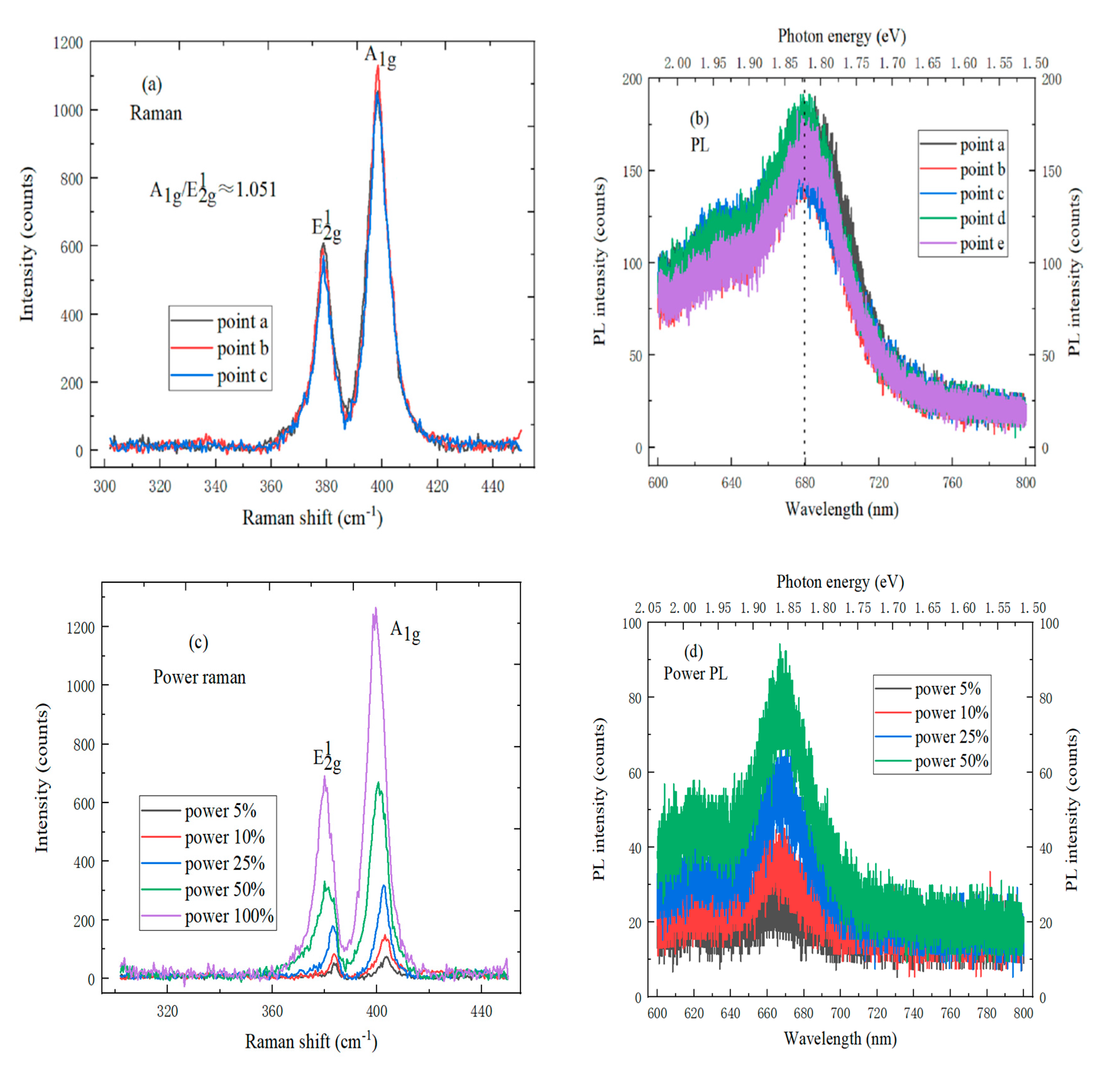
4.2. The Spectrum Characterization of Monolayer MoS2

In Figure 6a, the Raman spectrum of monolayer MoS2 has two characteristic peaks, wherein the E12g characteristic peak is at 379 cm−1, the position of A1g characteristic peak is 398 cm−1, and the ratio of A1g to E12g characteristic peaks is approximately 1.051. Besides, the Raman spectrum intensity and position of the MoS2 sample at different points are consistent, which shows that the monolayer MoS2 sample is highly uniform. It can be seen from Figure 6b that the strongest PL spectrum peak position of monolayer MoS2 on SiO2/Si substrate is at 681.2 nm, and the electron volt is 1.82 eV, which is the same as the direct band gap width of monolayer MoS2. Besides, the PL spectrum of monolayer MoS2 also has an exciton peak at 1.95 eV. The reason is that the Mo atom has 3d orbital electron interaction [25]. As shown in Figure 6c, the Raman spectrum intensity of MoS2 sample increases when the laser power increases; the positions of E12g and A1g characteristic peaks are blue-shifted simultaneously, which is caused by the n-type doped semiconductor characteristics of SiO2/Si substrate [26]. Figure 6d shows the PL spectrum of monolayer MoS2 under different laser powers. As the laser power increases, the strongest photoluminescence spectrum peak intensity of monolayer MoS2 increases, and the shape and position of characteristic peaks do not change. It can be judged that MoS2 on SiO2/Si substrate is monolayer, by characterizing and analyzing the Raman spectrum and photoluminescence spectrum of MoS2.

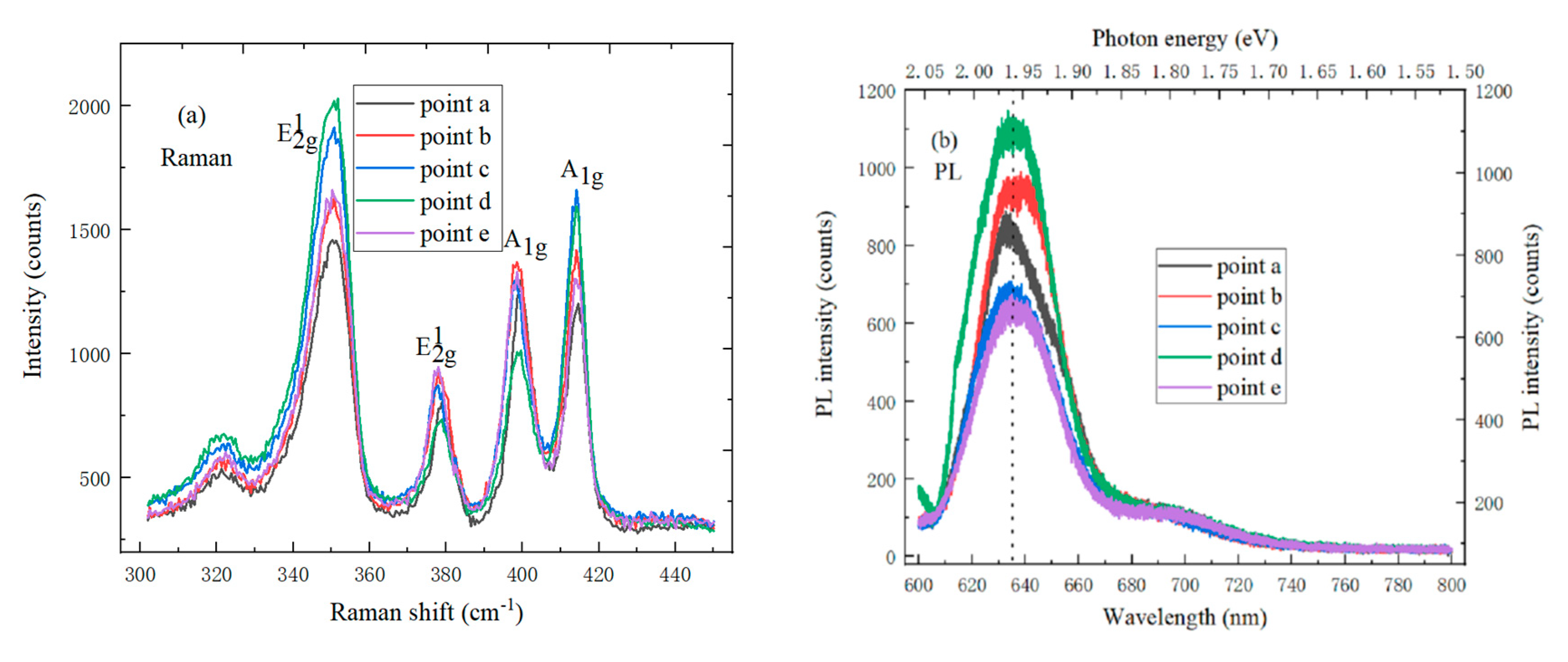
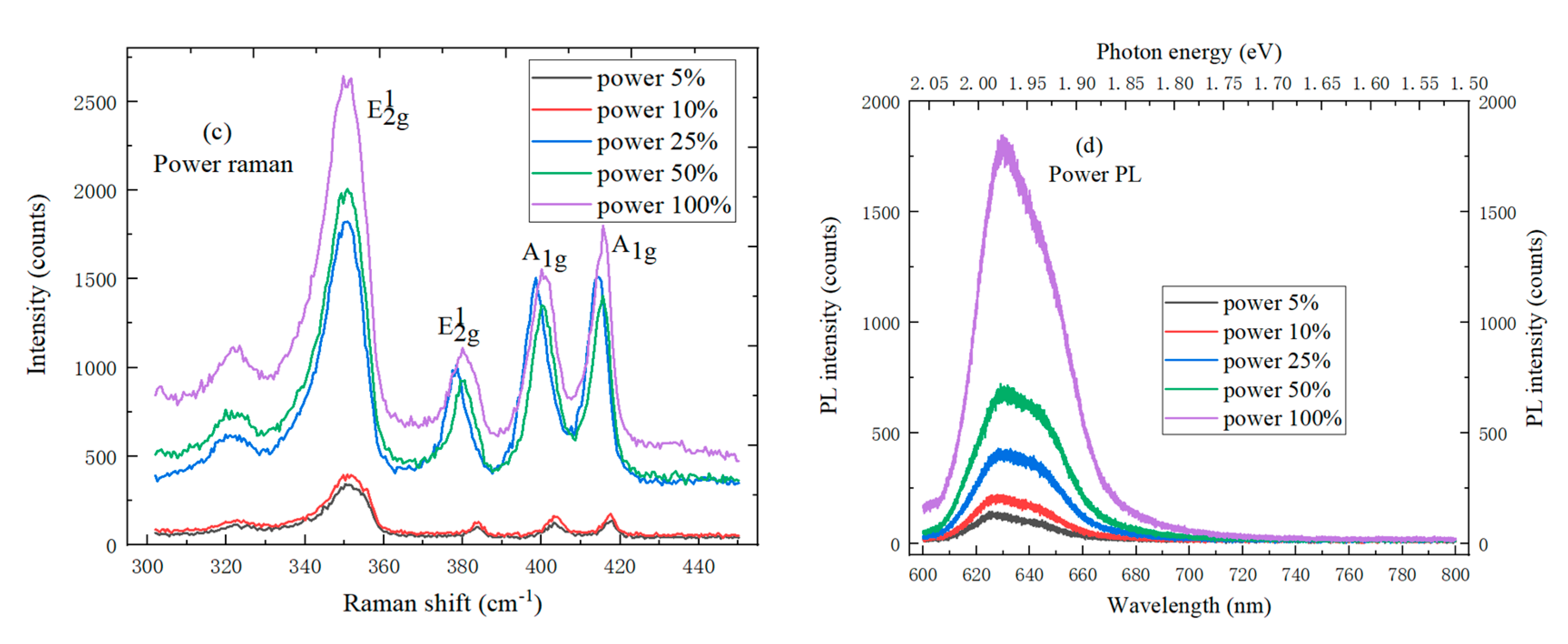
4.3. Spectrum Characterization of the MoS2/WS2 Heterojunction

The Raman spectrum of the MoS2/WS2 hetero-junction is tested with the 532 nm laser excitation wavelength, to evaluate vibration characteristics and thickness. There are E12g and A1g Raman active modes in the Raman spectrum of MoS2/WS2 hetero-junction, wherein the E12g is the in-plane optical mode that corresponds to the vibrational motion of Mo and S atoms in the x and y planes, while the A1g is an out-of-plane vibration mode that corresponds to the vibrational motion of two S atoms along the z unit cell axis [27]. It can be found that four Raman characteristic peaks, WS2-E12g, MoS2-E12g, MoS2-A1g, and WS2-A1g, appeared in the MoS2/WS2 hetero-junction region, and the corresponding peak positions are respectively located at 350 cm−1, 379 cm−1, 398 cm−1 and 413 cm−1. In the four Raman peaks of MoS2/WS2 hetero-junction, two peaks are the same as the Raman peaks of MoS2 film, and the other two peaks correspond to the Raman peaks of WS2 film. The four Raman peaks positions of MoS2/WS2 hetero-junction did not show red or blue shift, which indicates that WS2 and MoS2 did not affect the long-distance Coulomb interaction between the effective charges [28]. The photoluminescence spectrum can be used to identify the band gaps of WS2 and MoS2. Figure 7b shows the PL spectrum of WS2/MoS2 hetero-junction under the 532 nm wavelength. The PL peak positions of WS2 and MoS2 are respectively located at 635 nm (1.96 eV) and 682 nm (1.82 eV), which is due to the direct exciton transition energy of bottom layer MoS2 and top layer WS2. It can be seen by comparing and analyzing the PL spectrum of MoS2/WS2 vertical hetero-junction and single MoS2 or WS2 thin films that the PL peak position of MoS2/WS2 hetero-junction is the same as that of the single MoS2 or WS2 films, but the peak intensity of the MoS2/WS2 hetero-junction is much lower than that of the single WS2 films, which can be caused by interlayer exciton relaxation. At the interface between MoS2 and WS2 composites, electrons from the conduction band of WS2 are transferred to the conduction band of MoS2, and the holes from the valence band of MoS2 are moved to the valence band of WS2, which would cause the separation of photo-generated electrons and holes [29]. A slight PL position shift and an additional weak peak of 1.82 eV can be observed in the epitaxial MoS2/WS2 hetero-junction, which can be attributed to the recombination of spatially separated carriers. The two main factors of the PL spectrum quenching are the energy and charge transfer. In Figure 7c, the four characteristic peaks intensity of MoS2/WS2 hetero-junction gradually increases with the laser power increase, wherein the E12g and A1g characteristic peak positions of bottom layer MoS2 are blue-shifted, and the A1g characteristic peak position of top layer WS2 also shifted blue. Different laser powers on MoS2/WS2 hetero-junction would generate different heat, which can affect the Raman spectrum of MoS2/WS2 hetero-junction. The top layer WS2 may prevent the effective collection of Raman scattered signals from the bottom layer MoS2. Meanwhile, the Raman signal from WS2 is also weakened when it passes the bottom layer of MoS2, indicating that the bottom layer MoS2 can still affect the Raman intensity of the top layer WS2. Figure 7d shows the photoluminescence spectrum of the MoS2/WS2 hetero-junction under different laser powers. The strongest photoluminescence peak intensity of the MoS2/WS2 hetero-junction increases with laser power increase; the strongest photoluminescence spectrum position red-shifted, and the strongest photoluminescence spectrum shape of MoS2/WS2 hetero-junction also changes.

5. Conclusions

The 2D TMDs materials have different energy band structures and band gaps, so that the physical properties of 2D TMDs materials can be finely adjusted by stacking with each other. The large-area, high-quality monolayer MoS2 and WS2 materials are first prepared by APCVD method in this paper. Then, the MoS2/WS2 vertical hetero-junction is prepared by the dry transfer method, which can provide a well-defined interface between WS2 and MoS2 in the vertical dimension. The interface environment is the key factor affecting the performance of VDW hetero-structure modulation devices. The optimal reaction conditions of MoS2/WS2 vertical hetero-junction by the APCVD and dry transfer methods are obtained through experiments. The composite materials are divided into the MoS2, WS2 and MoS2/WS2 hetero-junction regions, according to the morphology evolution of the MoS2/WS2 vertical hetero-junction on the SiO2/Si substrate. Compared to the single MoS2 or WS2 materials, the PL spectrum characterization results show that the PL intensity of the MoS2/WS2 hetero-junction is reduced by half, which is due to the effective photoelectron-hole separation phenomenon which occurred during the recombination process. Meanwhile, the strong interlayer coupling and effective interlayer charge transfer of the MoS2/WS2 hetero-junction are systematically studied to strengthen the basic understanding of interlayer coupling, which can provide an unstructured and convenient method to explore the interface environment of the VDW hetero-structures. At the same time, the characterization results can help the mass production of various VDW hetero-junctions in future optoelectronic devices.

Author Contributions

Conceptualization and writing—original draft preparation, T.H.; methodology, S.W. and S.C.; validation, S.C. and K.Y.; writing—review and editing, H.L.; funding acquisition, H.L. All authors have read and agreed to the published version of the manuscript.

Funding

This research was funded by the National Natural Science Foundation of China (Grant No. U1866212 and 61904136), the Foundation for Fundamental Research of China (Grant No. JSZL2016110B003), the Major Fundamental Research Program of Shaanxi (Grant No. 2017ZDJC-26), the Innovation Foundation of Radiation Application (Grant No. KFZC2018040206). It was also supported by the Fundamental Research Funds for the Central Universities, and the Innovation Fund of Xidian University.

Conflicts of Interest

The authors declare no conflict of interest.

References

  1. Zhang, J.; Wang, J.; Chen, P.; Sun, Y.; Wu, S.; Jia, Z.; Lu, X.; Yu, H.; Chen, W.; Zhu, J.; et al. Observation of strong interlayer coupling in MoS2/WS2 heterostructures. Adv. Mater. 2016, 28, 1950–1956. [Google Scholar] [CrossRef] [PubMed]
  2. Zheng, J.; Yan, X.; Lu, Z.; Qiu, H.; Xu, G.; Zhou, X.; Wang, P.; Pan, X.; Liu, K.; Jiao, L. High-Mobility Multilayered MoS2 Flakes with Low Contact Resistance Grown by Chemical Vapor Deposition. Adv. Mater. 2017, 29, 1604540. [Google Scholar] [CrossRef] [PubMed]
  3. Zhang, W.; Huang, J.K.; Chen, C.H.; Chang, Y.H.; Cheng, Y.J.; Li, L.J. High gain phototransistors based on a CVD MoS2 monolayer. Adv. Mater. 2013, 25, 3456–3461. [Google Scholar] [CrossRef] [PubMed]
  4. Yang, P.; Yang, A.G.; Chen, L. Influence of seeding promoters on the properties of CVD grown monolayer molybdenum disulfide. Nano Res. 2019, 12, 823–827. [Google Scholar] [CrossRef]
  5. Shin, G.H.; Koo, B.; Park, H.; Woo, Y.; Lee, J.E.; Choi, S.Y. Vertical-tunnel field-effect transistor based on a silicon–MoS2 Three-dimensional–two-dimensional heterostructure. ACS Appl. Mater. Interfaces 2018, 10, 40212–40218. [Google Scholar] [CrossRef] [PubMed]
  6. Wang, J.; Yao, Q.; Huang, C.W.; Zou, X.; Liao, L.; Chen, S.; Fan, Z.; Zhang, K.; Wu, W.; Xiao, X.; et al. High mobility MoS2 transistor with low schottky barrier contact by using atomic thick h-BN as a tunneling layer. Adv. Mater. 2016, 28, 8302–8308. [Google Scholar] [CrossRef]
  7. Yu, W.J.; Liu, Y.; Zhou, H.; Yin, A.; Li, Z.; Huang, Y.; Duan, X. Highly efficient gate-tunable photocurrent generation in vertical heterostructures of layered materials. Nat. Nanotechnol. 2013, 8, 952. [Google Scholar] [CrossRef] [Green Version]
  8. Miao, J.; Hu, W.; Jing, Y.; Luo, W.; Liao, L.; Pan, A.; Wu, S.; Cheng, J.; Chen, X.; Lu, W. Surface plasmon-enhanced photodetection in few layer MoS2 phototransistors with Au nanostructure arrays. Small 2015, 11, 2392–2398. [Google Scholar] [CrossRef]
  9. Chen, J.; Zhao, X.; Tan, S.J.; Xu, H.; Wu, B.; Liu, B.; Fu, D.; Fu, W.; Geng, D.; Liu, Y.; et al. Chemical vapor deposition of large-size monolayer MoSe2 crystals on molten glass. J. Am. Chem. Soc. 2017, 139, 1073–1076. [Google Scholar] [CrossRef]
  10. Liu, K.; Zhang, L.; Cao, T.; Jin, C.; Qiu, D.; Zhou, Q.; Zettl, A.; Yang, P.; Louie, S.G.; Wang, F. Evolution of interlayer coupling in twisted molybdenum disulfide bilayers. Nat. Commun. 2014, 5, 4966. [Google Scholar] [CrossRef]
  11. Moriya, R.; Yamaguchi, T.; Inoue, Y.; Morikawa, S.; Sata, Y.; Masubuchi, S.; Machida, T. Large current modulation in exfoliated-graphene/MoS2/metal vertical heterostructures. Appl. Phys. Lett. 2014, 105, 083119. [Google Scholar] [CrossRef] [Green Version]
  12. Lee, C.; Yan, H.; Brus, L.E.; Heinz, T.F.; Hone, J.; Ryu, S. Anomalous lattice vibrations of single-and few-layer MoS2. ACS Nano 2010, 4, 2695–2700. [Google Scholar] [CrossRef] [Green Version]
  13. Yu, H.; Liao, M.; Zhao, W.; Liu, G.; Zhou, X.J.; Wei, Z.; Zhou, S. Wafer-scale growth and transfer of highly-oriented monolayer MoS2 continuous films. ACS Nano 2017, 11, 12001–12007. [Google Scholar] [CrossRef]
  14. Zhao, Y.; Luo, X.; Li, H.; Zhang, J.; Araujo, P.T.; Gan, C.K.; Wu, J.; Zhang, H.; Quek, S.Y.; Dresselhaus, M.S.; et al. Interlayer breathing and shear modes in few-trilayer MoS2 and WSe2. Nano Lett. 2013, 13, 1007–1015. [Google Scholar] [CrossRef] [PubMed] [Green Version]
  15. Yang, W.; Chen, G.; Shi, Z.; Liu, C.C.; Zhang, L.; Xie, G.; MCheng Wang, D.; Yang, R.; Shi, D.; Watanabe, K.; et al. Epitaxial growth of single-domain graphene on hexagonal boron nitride. Nat. Mater. 2013, 12, 792. [Google Scholar] [CrossRef]
  16. Shi, Y.; Zhou, W.; Lu, A.Y.; Fang, W.; Lee, Y.H.; Hsu, A.L.; Kim, S.M.; Kim, K.K.; Yang, H.Y.; Li, L.J.; et al. van der Waals epitaxy of MoS2 layers using graphene as growth templates. Nano Lett. 2012, 12, 2784–2791. [Google Scholar] [CrossRef]
  17. Zafar, A.; Nan, H.; Zafar, Z.; Wu, Z.; Jiang, J.; You, Y.; Ni, Z. Probing the intrinsic optical quality of CVD grown MoS2. Nano Res. 2017, 10, 1608–1617. [Google Scholar] [CrossRef]
  18. Chow, P.K.; Singh, E.; Viana, B.C.; Gao, J.; Luo, J.; Li, J.; Lin, Z.; Elías, A.L.; Shi, Y.; Wang, Z. Wetting of mono and few-layered WS2 and MoS2 films supported on Si/SiO2 substrates. ACS Nano 2015, 9, 3023–3031. [Google Scholar] [CrossRef] [PubMed]
  19. Wen, Y.N.; Xia, M.G.; Zhang, S.L. Size effect on the magnetic and electronic properties of the monolayer lateral hetero-junction WS2-MoS2 nanoribbon. Appl. Surf. Sci. 2016, 371, 376–382. [Google Scholar] [CrossRef] [Green Version]
  20. Xu, W.; Li, S.; Zhou, S.; Lee, J.K.; Wang, S.; Sarwat, S.G.; Wang, X.; Bhaskaran, H.; Pasta, M.; Warner, J.H. Large Dendritic Monolayer MoS2 Grown by Atmospheric Pressure Chemical Vapor Deposition for Electrocatalysis. ACS Appl. Mater. Interfaces 2018, 10, 4630–4639. [Google Scholar] [CrossRef] [PubMed]
  21. Li, X.; Li, X.; Zang, X.; Zhu, M.; He, Y.; Wang, K.; Xie, D.; Zhu, H. Role of hydrogen in the chemical vapor deposition growth of MoS2 atomic layers. Nanoscale 2015, 7, 8398–8404. [Google Scholar] [CrossRef] [PubMed]
  22. Lopez-Sanchez, O.; Alarcon Llado, E.; Koman, V.; Fontcuberta i Morral, A.; Radenovic, A.; Kis, A. Light generation and harvesting in a van der Waals heterostructure. ACS Nano 2014, 8, 3042–3048. [Google Scholar] [CrossRef] [PubMed]
  23. Lee, G.-H.; Yu, Y.-J.; Cui, X.; Petrone, N.; Lee, C.-H.; Choi, M.S.; Lee, D.-Y.; Lee, C.; Yoo, W.J.; Watanabe, K. Flexible and transparent MoS 2 field-effect transistors on hexagonal boron nitride-graphene heterostructures. ACS Nano 2013, 7, 7931–7936. [Google Scholar] [CrossRef] [PubMed]
  24. Kaasbjerg, K.; Thygesen, K.S.; Jacobsen, K.W. Phonon-limited mobility in n-type single-layer MoS2 from first principles. Phys. Rev. B 2012, 85, 115317. [Google Scholar] [CrossRef] [Green Version]
  25. Chae, W.H.; Cain, J.D.; Hanson, E.D.; Murthy, A.A.; Dravid, V.P. Substrate-induced strain and charge doping in CVD-grown monolayer MoS2. Appl. Phys. Lett. 2017, 111, 143106. [Google Scholar] [CrossRef]
  26. Frisenda, R.; Niu, Y.; Gant, P.; Molina-Mendoza, A.J.; Schmidt, R.; Bratschitsch, R.; Liu, J.; Fu, L.; Dumcenco, D.; Kis, A. Micro-reflectance and transmittance spectroscopy: A versatile and powerful tool to characterize 2D materials. J. Phys. D Appl. Phys. 2017, 50, 074002. [Google Scholar] [CrossRef]
  27. Heo, H.; Sung, J.H.; Jin, G.; Ahn, J.H.; Kim, K.; Lee, M.J.; Jo, M.H. Rotation-Misfit-Free Heteroepitaxial Stacking and Stitching Growth of Hexagonal Transition-Metal Dichalcogenide Monolayers by Nucleation Kinetics Controls. Adv. Mater. 2015, 27, 3803–3810. [Google Scholar] [CrossRef]
  28. Zhang, X.; Han, W.P.; Wu, J.B.; Milana, S.; Lu, Y.; Li, Q.Q.; Li, A.C.; Ferrari, P.H.; Tan, P.H. Raman spectroscopy of shear and layer breathing modes in multilayer MoS 2. Phys. Rev. B 2013, 87, 115413. [Google Scholar] [CrossRef] [Green Version]
  29. Lui, C.H.; Ye, Z.; Ji, C.; Chiu, K.C.; Chou, C.T.; Andersen, T.I.; Andersen, C.; Means-Shively, H.; Anderson, J.M.; Wu, T.; et al. Observation of interlayer phonon modes in van der Waals heterostructures. Phys. Rev. B 2015, 91, 165403. [Google Scholar] [CrossRef] [Green Version]
Sample Availability: Samples of the compounds MoS2/WS2 vertical hetero-junction...... are available from the authors.
Figure 1. (a) Schematic diagram of MoS2 or WS2 materials growth experiment by atmospheric pressure chemical vapor deposition (APCVD); (b) The temperature change diagram of MoS2 or WS2 materials experiment process by APCVD.
Molecules 25 01857 g001
Figure 2. Optical microscopy images of MoS2/WS2 vertical hetero-junction at different magnifications (a) 10×; (b) 50×; (c) 100× objectives.
Molecules 25 01857 g002
Figure 3. Field emission scanning electron microscope (FESEM) characterization of MoS2/WS2 vertical hetero-junction at different magnifications (a) 500×; (b) 1000×; (c) 1500×; (d) 2000×.
Molecules 25 01857 g003
Figure 4. Atomic force microscope (AFM) image of (a) MoS2; (b) WS2; (c) MoS2/WS2 vertical hetero-junction.
Molecules 25 01857 g004
Figure 5. (a) The Raman spectrum and (b) Photoluminescence spectrum of monolayer WS2 on SiO2/Si substrate at three different points; (c) Raman spectrum and (d) Photoluminescence spectrum of monolayer WS2 on SiO2/Si Substrate under different laser powers.
Molecules 25 01857 g005
Figure 6. (a) Raman spectrum and (b) Photoluminescence (PL) spectrum of monolayer MoS2 on SiO2/Si substrate at different points; (c) Raman spectrum and (d) PL spectrum of monolayer MoS2 under different laser powers.
Molecules 25 01857 g006
Figure 7. (a) Raman spectrum and (b) PL spectrum of MoS2/WS2 hetero-junction on SiO2/Si substrate at five points; (c) Power Raman spectrum and (d) Power photoluminescence spectrum of MoS2/WS2 hetero-junction on SiO2/Si substrate.
Molecules 25 01857 g007aMolecules 25 01857 g007b

