1. Introduction
In recent years, there has been a remarkable surge in the application of planar solenoids embedded in printed circuit boards (PCBs) owing to their facile fabrication and seamless integration with other circuitry components [
1,
2]. These versatile solenoids have found applications in a wide array of fields, including high-frequency inductors, helical antennas, RF IDs, power conversion coils, and resonators, leading to widespread adoption by various industries seeking cost-efficient solutions [
3,
4,
5,
6,
7,
8]. The escalating adoption of planar solenoids in various products hints at their significant potential in shaping the future of electronics [
9]. However, despite their growing popularity, a dearth of comprehensive analytical reports exists, leaving crucial aspects of their performance relatively unexplored. One such aspect is the investigation of fabrication limits using current industry standards, which have received insufficient attention. To address these gaps in knowledge, this paper presents a comprehensive analytical study of planar solenoids fabricated within PCBs, shedding light on key parameters, such as inductance, capacitance, resistance, and quality factor. Furthermore, the research endeavors to determine the smallest attainable size for fabrication, adhering to existing industry-level standards. Additionally, the analytical method employed in this study effectively verifies the design of a novel resonator, demonstrating the practical viability and potential performance advantages of utilizing solenoids embedded in PCBs. The findings of this study not only contribute to the understanding of planar solenoid integration but also serve as a valuable resource for future design considerations, encouraging further exploration and adoption of this promising technology in diverse electronic applications.
While some progress has been made in enhancing the quality factor using these fabrication techniques, the optimization of the quality factor for resonator structures with fixed dimensions by varying the position of its elements remains unaddressed. To optimize the quality factor at the dominant resonance frequency for a given resonator structure, the zero-pole transfer in the transfer function of the device circuit can be employed [
10]. Optimizing the dominant pole of the circuit using zero-pole transfer significantly increases the quality factor of the dominant pole resonator. Increasing the distance between the near pole or zero and the dominant pole significantly elevates the Q-factor. The transfer of poles was utilized to increase the frequency separation between the pole and zero, eliminating the effect of pole–zero cancellation. However, the poles should not be too close to each other to avoid any alteration in the dominant resonant response and to achieve the optimum quality factor. Experimental optimization of the Q-factor was achieved by altering the location of a series capacitance in the resonator circuit to transfer the poles and maximize the Q-factor.
This article presents the design, fabrication, and testing of a micro-solenoid resonator aimed at achieving optimized performance. The resonator consists of a micro-solenoid embedded within an RT/Duroid 5880 circuit board, which helps to minimize stray capacitance and field losses [
11]. To increase the resonance frequency and transfer the dominant pole, a series capacitor was introduced between two turns of the solenoid, creating a coupling connection between the coil turns. This capacitor also adds a pole to the overall circuit’s transfer function. The fabrication process involved the creation of a thin dielectric layer between two conductors within the via, which provided the desired capacitance.
Figure 1 illustrates a schematic diagram of the resonator. The results demonstrate that the resonance frequency can be altered by changing the location of the capacitor within the via. Consequently, the dominant frequency pole in the circuit is transferred to a new position. Additionally, the addition of the series capacitance in the solenoid transforms the two-pole circuit into a four-pole circuit with non-zero poles. These new poles have smaller real parts due to reduced resistivity.
Analytical modeling of the circuit was conducted using the π-circuit model to determine the location of the zeros and poles in the frequency response characteristic function. Furthermore, an electromagnetic simulation was performed using Ansys-HFSS software. The fabricated devices were experimentally tested by measuring their S-parameters using a microwave probe station. Both the resonance frequency and quality factor were extracted from the experimental data, which exhibited close agreement with the modeling and simulation results. These findings have been successfully applied to narrowband microwave filters, providing high-quality factors at gigahertz frequencies. The utilization of standard PCB fabrication has the potential to reduce the complexity and cost associated with commercializing the device, particularly when compared to on-chip resonators and similar MEMS structures [
12].
2. Theory
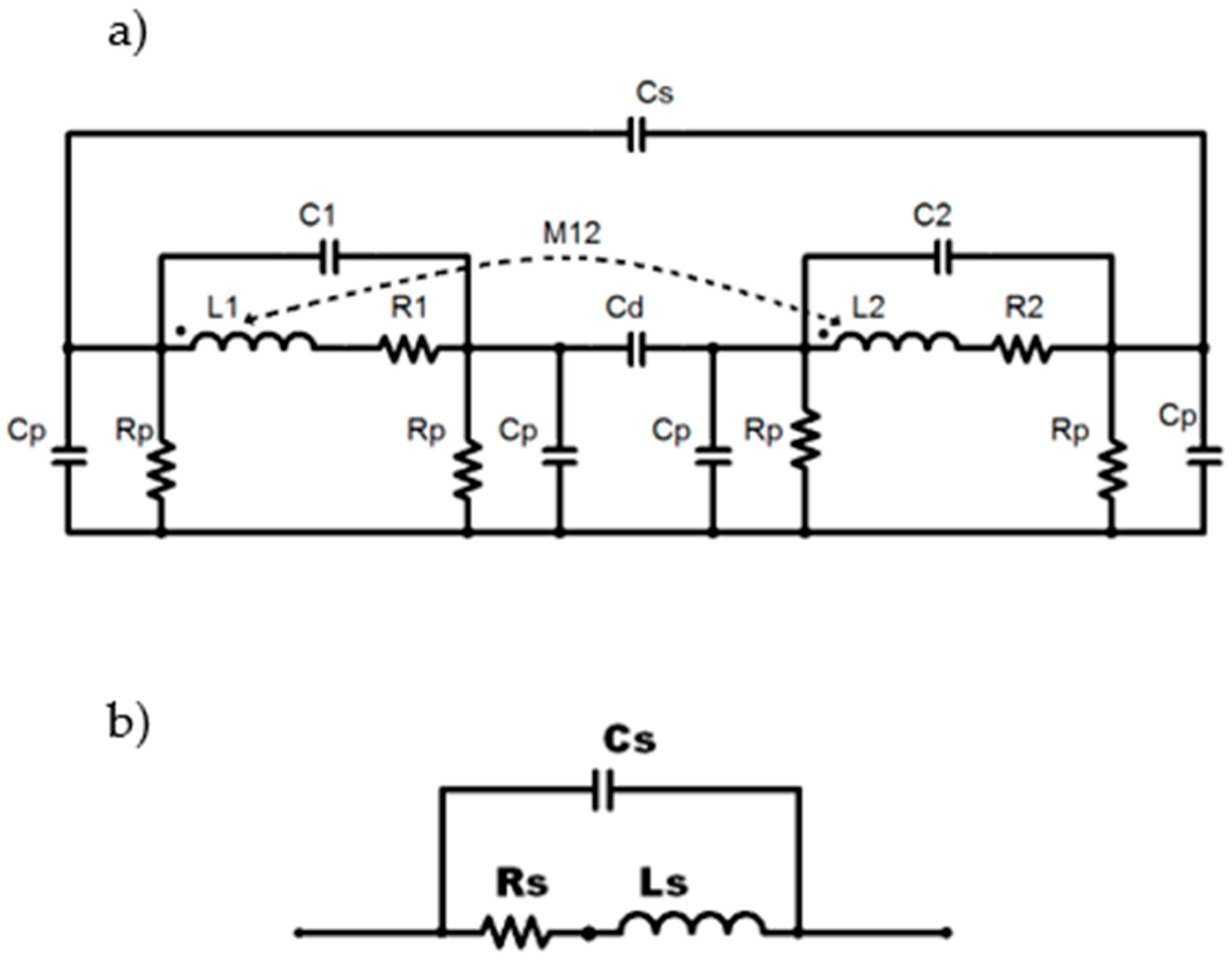
To establish a theoretical model for the double-zero double-pole resonator, a comprehensive approach was employed to provide a thorough description. This methodology involved developing a complete circuit representation using the device parameters. Subsequently, a simplified model was applied to each zero-pole pair of the resonator. The simplification process was justified by adopting a similar methodology previously introduced by Grandi et al. for the evaluation of stray capacitance in solenoids [
8,
13]. The equivalent circuit model of the resonator is depicted in
Figure 2a, while the simplified circuit is illustrated in
Figure 2b. Previous studies extensively investigated the single and double π-models of microfabricated spiral and solenoid inductors and resonators to evaluate the components of the resonator [
14,
15,
16]. The GreenHouse–Grover approach was used to determine the mutual and self-inductance between each segment, which was then incorporated into the evaluation of overall inductance [
17,
18]. The capacitive components of the model were formed by three capacitances: stray capacitance (Cs), parallel capacitance (Cp), and series capacitance in the via (Cd). The resistance of the device was accounted for by incorporating the series conductor resistances, taking into consideration the skin effect at high frequencies. After building the circuit using these parts, the overall circuit model was analyzed depending on where the zeros and poles were placed. To split the circuit into two identical circuits within a single-turn circuit, a series capacitance was added. Additionally, this series capacitance is acting as a second pole in the frequency response.
2.1. Inductances
The self-inductance of a cylindrical via in the PCB is called L
cs and has an approximate value of [
17]:
where
h is the height and
w is the diameter of the via in centimeters. The value of
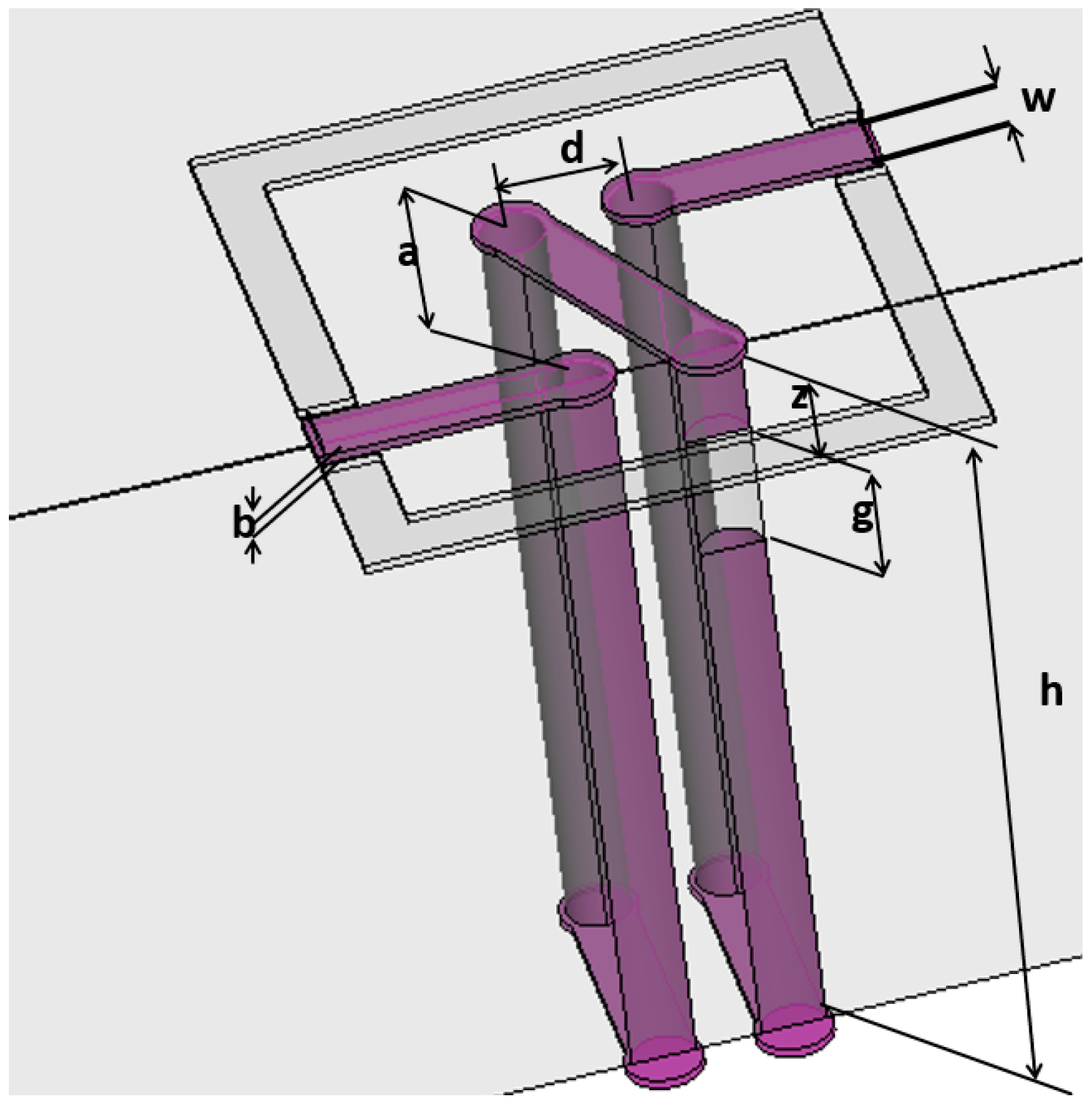
w is also equal to the width of the surface conductors. The dimensions and size for a single-turn resonator are shown in
Figure 1. If
b would be considered as the thickness of copper and
w as the width of the segment in centimeters, then the self-inductance for a wire of rectangular shape with the length of a is
Lrs and is formulated as [
17]:
It is possible to assess the reciprocal inductance of
M between each pair of segments using [
17]:
If the current in both segments moved in the same direction, the sign will be positive; if not, it will be negative. The formula for
K is:
where
D could be found using the following equation if
d is be the distance between the centers of the two conductors.
The sum of all self-inductances and mutual inductances for
m segments of the coil equals the total inductance of
Ls:
The inductance of partially filled segments in via would be evaluated by considering the filled area of the column for each side. Self-inductances of L
1 and L
2 have been evaluated using this method, and the mutual inductance between two individual inductances of the resonator could be calculated using (4) and the second part of (6). This was illustrated as M
12 in
Figure 2. In this circuit, a large air gap between the resonators and the ground made the parallel impedance large enough to make the current in series branches almost equal. Considering an equal current in the series branches, the values of L
1 and L
2 were calculated using (6), including the total value of (4). This would help to evaluate the circuit without having the extra term of M
12, as it would be given next in [
17].
2.2. Capcitances
The values of C
1 and C
2 in
Figure 2a are also evaluated by the Equation (6). In a single-turn model, the value of n’ depends on the position of dielectric in via and it will be substituted by
n’ for the conductor circuit with the top surface segment.
or it will be
n” for the conductor with the bottom-side surface segment:
where the value of
ns will be equal to one for a single turn model. Each segment also produces a capacitance to the ground. The two-port network’s (
Cp) parallel capacitive features were created. It was made up of the upper segment capacitances (
CU) and the lower segment capacitances (
CL). Because of the great distance between the resonator the and ground, the relative permittivity for
CU has been calculated as
ϵ0. A more detailed calculation of the capacitances can be found in references number [
19], and [
8]. The equivalent value for
Cp is:
where
CL and
CU are:
Between the conductor and the ground is
lsub, which is filled with air. The capacitance in the via is calculated with the following formula using two circular conductors of the copper column and the dielectric of thickness
g between them.
2.3. Resistances
The resistance in series, which is shown in Equation (13), included the resistances of surface conductors in series with the resistances of the columns. The skin effect also should be considered for this calculation.
The constant
c is considered one in this experiment [
14]. The resistivity of copper is
ρ and the value of
n3 follows the same modification as it had for the evaluation of capacitances. The skin depth is
δ and it has been given by:
where
µ is the permeability of copper and f is the working frequency. The circuit parameters evaluated for different dielectric locations have been evaluated and illustrated in
Table 1.
3. Circuit Model
The parallel LC tank circuit is presented as a series branch of the two-port network in a π -circuit model.
Figure 2b shows an illustration of this LC tank. This branch’s transfer function is given by:
It demonstrates that the circuit contains two poles and one zero. The poles are:
There are two complex conjugate poles in the model as a result. Two circuits have been created for the circuit in
Figure 2a. A capacitor has been placed in the center of this circuit, which has its component parts split. The previous section provided details on how this capacitance was created. The transfer function of a circuit with a double pole resonator is given by Equation (15). Equation (17) has looked at a similar procedure for an inductor with two turns and a coupling capacitor in between. Inductors with several turns should be considered of having more than two poles.
The common definition for quality factor of such resonators based on the resonance frequency and bandwidth are given in Equation (18), and the quality factor of resonator can be evaluated using that Equation (5), [
20]:
The presence of a pole in close proximity to the imaginary axis within the frequency response curve results in a local maximum and can be interpreted as a resonance frequency. This behavior arises from the rapid phase change exhibited by the overall function. When the frequency approaches the vicinity of the first pole in the circuit, it induces the most significant phase variation. While the remaining poles also contribute to local phase changes, they are influenced by the preceding poles and are not situated near the imaginary axis. Consequently, these subsequent poles yield lower quality factors as the frequency increases. The determination of the quality factor, denoted as Q, is achieved independently of the specific application and relies on Equation (18) for its extraction.
The analytical modeling of the circuit presented in
Figure 2b, employing Equation (17), reveals the existence of five poles and four zeros. One of the poles, located at the origin, can be disregarded due to its minimal impact on the dominant pole. Consequently, attention is directed towards the remaining zeros and poles. By altering the position of the dielectric within the column of capacitance, the locations of the poles and zeros can be modified.
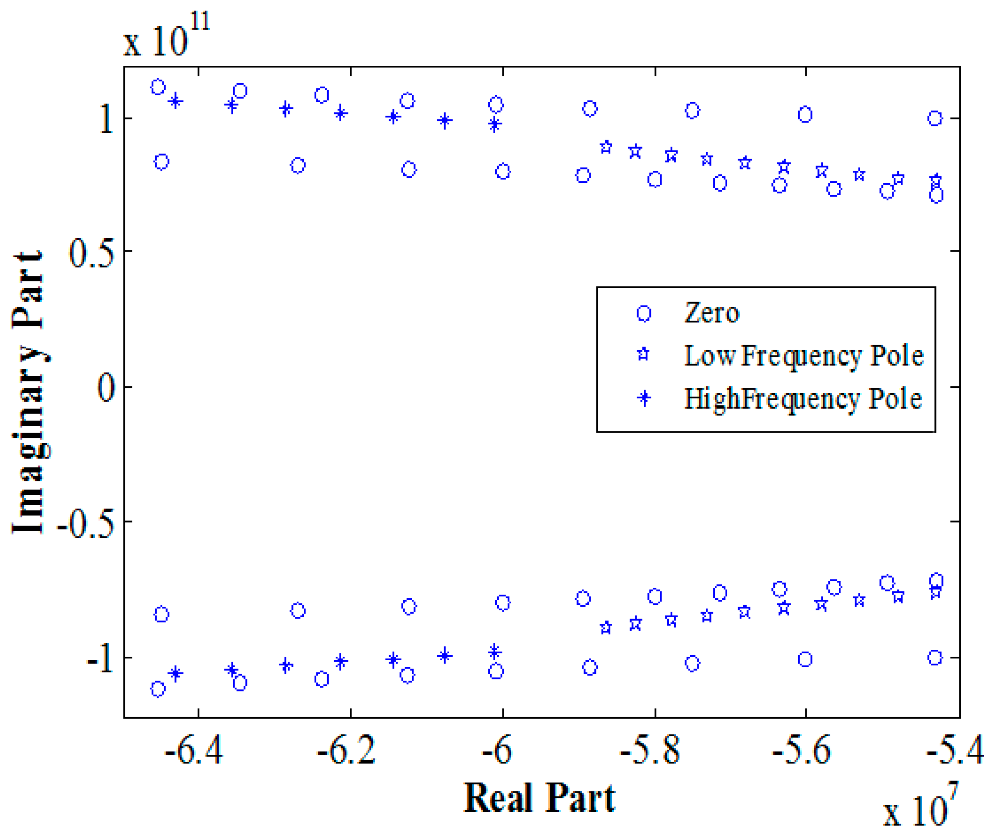
Figure 3 presents the variations in the pole and zero values corresponding to different positions of the dielectric, as demonstrated by the experimental results. When the dielectric is shifted towards the middle of the solenoid or, in other words, when it assumes lower values of z, the pole associated with lower frequencies relocates to higher frequency regions. Moreover, it moves farther away from the imaginary axis. Notably, even though the pole is positioned at a greater distance, it remains the dominant pole until it becomes proximate to the high-frequency pole. This behavior can be observed in
Figure 4, which illustrates the changes in the pole separation as the dielectric shifts to higher z values. It is worth noting that if the low-frequency pole is in close proximity to a zero, pole–zero cancellation can occur, leading to a reduction in the quality factor.
The values of poles and zeros for different dielectric locations are illustrated in
Figure 3. When the dielectric moves to the middle of solenoid, or in the other word it possesses lower values of z, then the lower frequency pole moves to higher frequencies. It would also move farther distance with respect to the imaginary axes. Even though it is farther, it remains as the dominant pole until it is very close to the high-frequency pole.
Figure 4 shows the change in distance between poles when the dielectric goes to higher z values. If the low-frequency pole would be near to a zero, then the pole–zero cancellation could damp the quality factor.
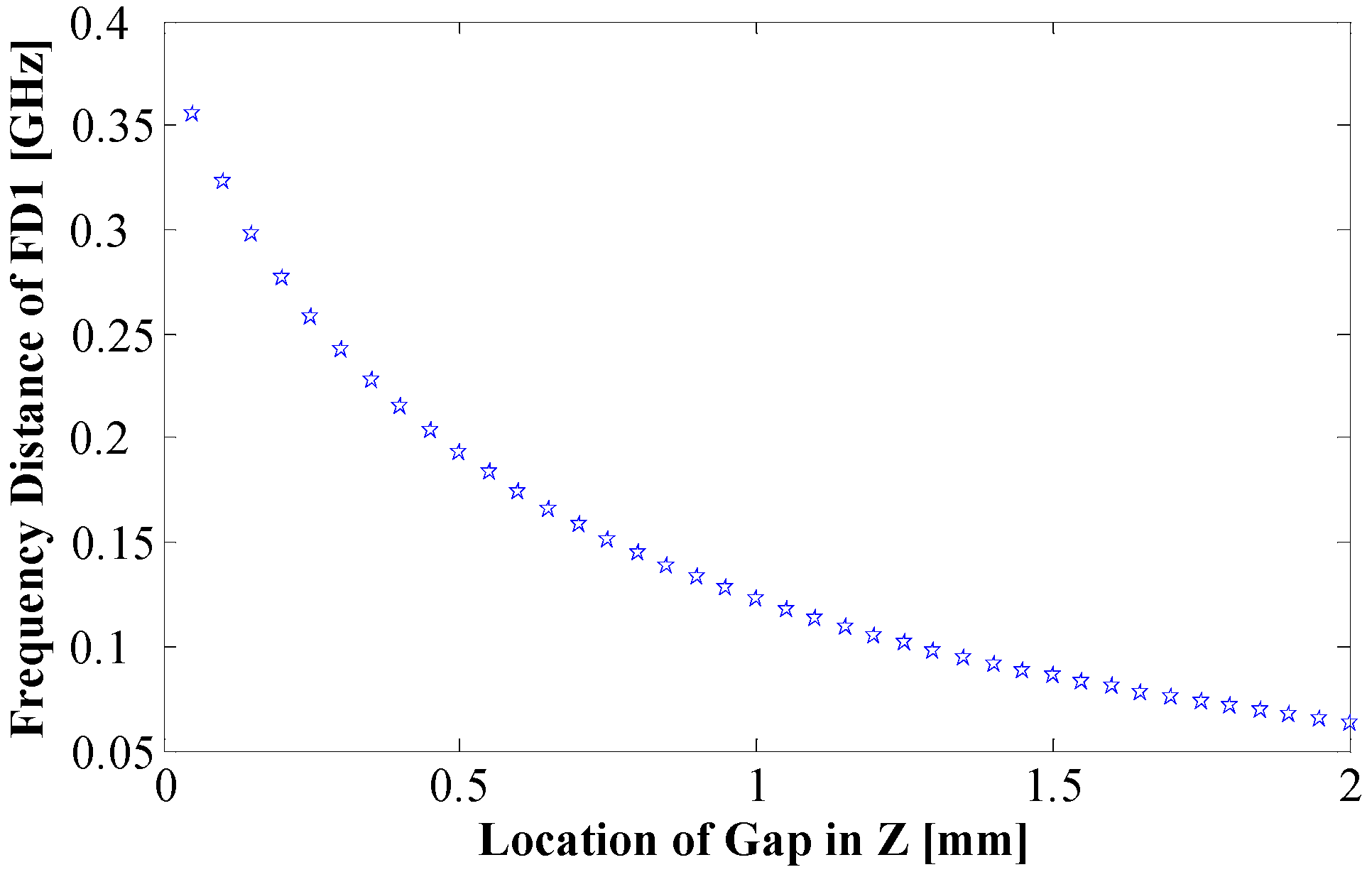
To formulate the frequency distance between the low frequency pole and the closest zero, we can name it FD1 as follows:
Figure 5 provides a visual representation of the phenomenon in which the low-frequency pole of the resonator moves away from its nearest zero as the dielectric reaches lower z values. This separation between the pole and its nearest zero contributes to an enhancement in the quality factor until the dominant pole, associated with the low-frequency response, approaches the second pole. In our experimental investigations, this occurrence was observed when the value of z fell below 0.3 mm.
4. Fabrication
The fabrication of three-dimensional (3D) structures using Duroid
TM material finds diverse applications in the development of microstrip antennas, interconnects, and cavity resonators [
21]. RT/Duroid
TM 5880, with a low relative permittivity of 2.2, exhibits a high fringing field in microwave frequencies while maintaining low electromagnetic field loss. To fabricate an efficient coil using vias in the microwave range, it is crucial to maintain low resistivity and compact dimensional characteristics. For compatibility with standard printed circuit board fabrication processes, a drilling size of 125 µm radius was employed, resulting in a conductor width and pitch size of 250 µm. The surfaces were clad with a 35 µm copper layer followed by silver immersion layer technology. The vias were electroplated to form the columns. This is the smallest radius and pitch size, and only very limited numbers of PCB manufacturers can make it in a board of over 3 mm thickness. This custom-designed board pushes the limits of PCB manufacturing to verify the maximum quality factor possible to make using planar helical resonators.
Previous experiments have demonstrated higher quality factors (Q-factors) for taller solenoids [
22]. Thus, a Duroid
TM substrate with a thickness of 3.02 mm was utilized. To create a capacitance within the vias, the electroplating process for specific vias was halted at a predetermined height. For a single-turn solenoid on a 3.02 mm thick Duroid
TM board, the electroplating was stopped at 2.2 mm. The electroplating rate for a current density of 20 mA/cm
2 was measured to be 350 nm/min. The via was sealed with a dielectric material by introducing KMPR negative photoresist inside the via, which was subsequently dried in an oven for 40 min at a temperature of 90 °C. The remaining columns were then electroplated up to the surface.
To ensure a desired dielectric thickness of 0.5 mm, the via was drilled to a depth of 375 µm with a diameter of 0.250 mm. Additional steps, such as photolithography and gold sputtering, were performed on the surface conductors to mitigate surface oxidation. The surface conductor comprised a 375 μm thick copper layer electroplated within the via to act as a cover, followed by a top connector layer of 35 µm thick copper.
Figure 6a–f provide a visual depiction of the fabrication process steps, while
Figure 6g showcases the final fabricated device.
5. Discussion and Results
Fabricated resonators were measured using a HP8363 network vector analyzer and GSG Cascade Micro-tech probes. The samples were put into the microwave probe station, and the pads were touched using GSG probes. Then, using the network vector analyzer, frequency ranges were scanned, and insertion loss (S12) was measured automatically. The short-open-load-thru (SOLT) calibration was done by an impedance standard substrate (ISS). De-embedding is important in removing the parasitic effects of the ports [
23]. De-embedding of the pads carried out after conversion of S-parameters to Y-parameters.
The Y-parameters of an open pad were subtracted from the measured parameters of a resonator in the pad, and the new Y-parameters were used to calculate the S-parameters. More details about the de-embedding steps have already been published [
24]. The findings indicate that the introduction of a series capacitor in the center of an embedded solenoid transforms the resonator with two complex conjugate poles into a resonator with four complex conjugate poles. The size of the capacitor determines the minimum frequency at which the device begins to transmit signals. In this experiment, a 0.5 mm gap filled with photoresist as a dielectric material served this purpose. Design considerations revealed that the fabrication of very thin dielectric layers, less than 0.4 mm thick, prevented the solenoid from forming a double resonator circuit.
The results demonstrate that, for this application in a double-turn solenoid, the resonance frequency tends to approximately double. However, increasing the number of turns beyond two does not result in doubling the resonance frequency. Higher-turn solenoids exhibit multiple resonance frequencies, and while their first resonance may be suppressed, their second resonance becomes dominant. Modeling efforts showed close agreement with the simulation, achieving a quality factor of 480 at 12.27 GHz.
Table 2 presents the simulation results for five different dielectric positions along with the corresponding measured frequency and quality factor. These results highlight the circuit’s sensitivity to the positions of its zeros and poles. The S21 parameters for four of the simulated resonators are plotted in
Figure 7.
Figure 8a provides a visual comparison of the measured and simulated S21 responses of a one-turn resonator. It is evident that the first poles in the simulation and measurement occurred at 12.27 GHz and 12.25 GHz, respectively, indicating a close match between the simulation and the fabricated device. However, the second poles occur at different frequencies. The measurement results revealed a second pole at 16.15 GHz, which appeared 740 MHz earlier than the corresponding pole in the simulation, which was at 16.89 GHz. This discrepancy may have arisen from inaccuracies in drilling and the creation of a smaller dielectric size. An unintended increase in the parameter “z” coupled with a decrease in “g” can lower the frequency of the second pole. This effect is caused by the elevated values of L2 and C2. The evaluation of the Q-factor for the fabricated device can be accomplished using Equation (18) and referring to
Figure 4b.
The extraction of the quality factor was performed using S21 measurements, resulting in a maximum quality factor of 306 at a frequency of 12.25 GHz for a two-turn solenoid. However, this value is lower than the previously calculated value of 480 obtained from simulations. The main reason for this discrepancy lies in the movement of the second pole towards the first pole in the measurement circuit, which leads to a reduction in the quality factor of the dominant pole.
The sensitivity of the resonator is primarily influenced by the copper plating, which limits the attainable quality factor, resulting in higher values than those observed in bulk copper. It is important to note that the quality factor of a double pole resonator is highly sensitive to the positioning of the poles relative to each other. The results of this experiment indicate that in order to achieve a high quality factor, the poles should not only be close to the imaginary axis but also maintained at a significant distance from each other. The highest quality factor for both poles is achieved when they are at least 5 GHz apart.
A previous study by Zhang demonstrated the tuning of the resonator using zero transmission to fabricate bandpass filters [
25]. In this paper, we not only investigate zero and pole transmission, but also explore the impact of resonator dimensions and the optimization of the quality factor using resonator elements.
This work presents a commercially manufacturable inductive resonator with a quality factor of 306 at a resonance frequency of 12.25 GHz, which is more than three times the quality factor reported by Melik et al. for an on-chip resonator at 15 GHz [
2]. Additionally, the current resonator achieves a f.Q product of 3.75 × 10
12, surpassing the maximums of 1.7 × 10
12 reported by Rinaldi et al. for contour-mode resonators [
26] and by Gu et al. of 1.2 × 10
9 [
27].
The fabrication of such narrow-band microwave filters can significantly enhance the efficiency of high-frequency circuits. The compact size of this resonator, which occupies only 10 mm2 of the printed circuit board, is noteworthy. In comparison, a ring resonator designed for the same working frequency would require a much larger captured area of 625 mm2. The small size of the proposed resonator allows for easy integration near integrated circuits using standard PCB fabrication techniques.
6. Conclusions
In conclusion, this paper presented the design, simulation, fabrication, and optimization of a novel off-chip solenoid resonator embedded in a printed circuit board (PCB). The resonator design incorporated embedded copper vias and surface conductors to form a rectangular coil, with a series capacitance introduced to enhance performance at higher frequencies. Through pole transfer analysis and optimization, the resonance frequency was increased to 12.25 GHz, and the quality factor (Q-factor) was elevated to 306. The research demonstrated that the optimized resonator design achieved a superior Q-factor compared to silicon-based counterparts. The use of a low-cost standard PCB fabrication technique offers simplified design and ease of fabrication. The analytical lumped circuit model used in the study closely matched the measured S-parameters and electromagnetic simulation results. The study addressed the challenge of optimizing the quality factor for resonator structures with fixed dimensions by varying the position of its elements. By employing zero-pole transfer in the transfer function of the device circuit, the dominant pole of the circuit was optimized, resulting in a higher Q-factor. Experimental results showed that altering the location of the series capacitance within the via allowed for tuning of the resonance frequency and transfer of the dominant pole to a new position.
Overall, this novel high-Q-factor compact resonator has potential applications in microwave filters for wireless communication devices and biomedical sensors. Its simplified design, ease of fabrication, and improved performance make it a promising candidate for practical implementation and commercialization, especially when compared to on-chip resonators and MEMS structures. Further research and development can explore the integration of this resonator in specific microwave applications to unlock its full potential.


