
Surface-Sensing Principle of Microprobe System for Micro-Scale Coordinate Metrology: A Review


Department of Precision Engineering, The University of Tokyo, Tokyo 113-8654, Japan
Metrology 2022, 2(1), 46-72; https://doi.org/10.3390/metrology2010004
Submission received: 7 October 2021
/
Revised: 16 December 2021
/
Accepted: 10 January 2022
/
Published: 20 January 2022
Abstract
:Micro-coordinate measuring machines (micro-CMMs) for measuring microcomponents require a probe system with a probe tip diameter of several tens to several hundreds of micrometers. Scale effects work for such a small probe tip, i.e., the probe tip tends to stick on the measurement surface via surface adhesion forces. These surface adhesion forces significantly deteriorate probing resolution or repeatability. Therefore, to realize micro-CMMs, many researchers have proposed microprobe systems that use various surface-sensing principles compared with conventional CMM probes. In this review, the surface-sensing principles of microprobe systems were the focus, and the characteristics were reviewed. First, the proposed microprobe systems were summarized, and the probe performance trends were identified. Then, the individual microprobe system with different sensing principles was described to clarify the performance of each sensing principle. By comprehensively summarizing multiple types of probe systems and discussing their characteristics, this study contributed to identifying the performance limitations of the proposed micro-probe system. Accordingly, the future development of micro-CMMs probes is discussed.
1. Introduction
A coordinate measuring machine (CMM) is a measuring instrument that can measure three-dimensional (3D) shapes of an object, including a probing system to detect an object’s surface, a positioning stage system to move either the probing system or the object, length scales to determine the coordinate of detected points by the probing system, as well as software to control the entire measurement [1]. Although X-ray-computed tomography has recently been developed [2,3], CMMs are still the most reliable measurement system for evaluating object shapes, dimensions, postures, and positions. Therefore, CMMs are generally used in industry as standard measurement systems [4]. However, manufacturing technologies have significantly developed to produce miniature parts, including small-scale shapes or components such as microgears, inkjet nozzles, and microholes [5,6,7,8,9]. Therefore, CMMs with nanoscale accuracy have been in high demand for evaluating the dimensions and shapes of these micro-scaled products. Takamasu et al. proposed the concept of a nano-CMM in 1996 [10]. Furthermore, other researchers, institutes, and companies have addressed the development of micro-/nano-CMMs [11,12,13,14,15,16,17,18]. Although there are different concepts for highly accurate CMMs, the representative specifications shown in Table 1 are important for micro-CMMs. Many names for CMMs with nanoscale accuracy have been proposed; however, in this study, the term “micro-CMM” is used. The required specifications of micro-CMMs are approximately one-hundredth of the size of conventional CMMs (Table 1), which is a significant challenge to achieve. Currently, micro-CMMs are commercially available, as summarized in [19]. The positioning system and scale must achieve high accuracy (Table 1). Most conventional CMMs do not meet the Abbe principle; however, for micro-CMMs, Abbe error-free structures are required to meet high accuracy. To meet the Abbe principle, metrology frames with interferometers are often used [20,21,22,23,24]. Figure 1a shows an Abbe error-free structure design example. The three laser interferometers for the X-, Y- and Z-axes are aligned to the probe tip of the probe system and measure the displacement of the metrology frame. In addition to the Abbe error, thermal drift is an important factor for reducing measurement uncertainty of the micro-CMMs. Therefore, in the micro-CMM structure, low thermal expansion materials such as Zerodur® and InverTM were used (Figure 1b) [11,22,23]. Moreover, it is important to separate heat sources. In the example of Figure 1, a stabilized He–Ne laser was isolated. For micro-CMMs, not only were these proposed, but many other intelligent designs to minimize the measurement uncertainty of the positioning stage have been presented. Consequently, the positioning stage achieved remarkably low uncertainty of as small as 50 nm or less [25,26]. The positioning stage shown in Figure 1 is the highly precise positioning system developed by Jager and Manske [25], which is now commonly used for micro-coordinate metrology. This intelligent system has a working range of 25 × 25 × 5 mm3 and sub-nanometer stability.
In terms of micro-CMMs, probe systems [9,26,27] are difficult to establish. The probe system with conventional CMMs performed excellently, with a repeatability of several tens of nanometers. However, as a microprobe system, its probe system structure is difficult to use. The probe system for micro-CMMs must be miniaturized (Table 1). Conventional touch-trigger probe mechanisms are no longer adequate for probe systems of micro-CMMs (microprobe system) because of the scale effect. Generally, the probe tip makes contact with the surface of the objects to detect their surface. At the microscale, this conventional mechanism may not function properly. This is because the dominant force acting on the probe tip transitions from volume forces such as gravity to surface forces such as adhesion forces. Therefore, probe tips tend to stick to the surface, thus degrading the detection repeatability. The measuring force is another reason. Even when the measuring force is reduced, the contact pressure remains relatively high, which causes surface damage. Because of these effects, it is difficult to use conventional mechanisms of the touch-trigger probe. Therefore, to date, different types of probe systems have been proposed. The proposed microprobe systems were well summarized in several review studies [28,29,30]. The overall probe systems for coordinate metrology, including conventional and microprobe systems, were summarized in [28]. Ref. [29] describes early-stage microprobe systems developed in the early 2000s. Certain microprobe systems described in this review have been realized for commercialization. Many microprobe systems have been developed to date; they are classified in two types: contact probes, which have a mechanism that can detect contact with high sensitivity; and probes that use the interaction between the probe tip and measurement surface to detect the measurement surface. Ref. [30] specifically focuses on summarizing the former type of the microprobe system. For the latter microprobe system, various types of probe systems using near-field physical phenomena acting on the probe tip and measurement surface have been proposed. Multiple unconventional surface-sensing principles that use physical interaction phenomena with the measurement surface rather than physical contact have been proposed, and their potentials have been explored.
In this study, the interactions between the probe tip and measurement surface were the focus, i.e., what type of physical interaction was used to detect the measurement surface. From this viewpoint, the microprobe systems for coordinate measuring systems were reviewed. By comprehensively summarizing various types of probe systems and discussing their characteristics, the performance limitations of the currently proposed micro-probe system were unveiled. Furthermore, the future development of micro-CMM probes was discussed.
2. Overview of Microprobe System for Coordinate Metrology
2.1. Issues for Microprobe System
This section discusses factors that must be considered when developing a microprobe system for micro-CMMs. First, the most different specification is the size of the probe tip. The size of the probe tip in CMM measurements directly affects the measurement’s accessibility; therefore, a small probe tip is required for micro-CMMs. Conventional probe systems have probe tips as large as millimeter-scale in diameter; typically, several millimeters. However, the microprobe systems require a few hundred to several dozens of micrometers in diameter (Table 1), i.e., the size of the probe tip must be reduced to one-fiftieth to the hundredth of the conventional probe tip. Due to the scale effect, the physical phenomena which contribute to the microprobe tip differ from conventional probes at the microscale. As a result of this disparity in a dominant physical phenomenon, various effects of these different physical phenomena should be considered.
Surface forces vary significantly depending on the material, surface properties, and environment. Figure 2 shows the surface forces working on the microprobe tip. The surface forces become increasingly more prominent than gravity when the size of the microprobe tip is less than a few millimeters. Surface forces are several orders of magnitude greater than gravity at scales of several tens to several hundred micrometers in diameter [31,32,33,34]. Therefore, surface forces attract the probe tip to the surface when the probe tip is close to the measurement surface [35]. Although surface forces can be reduced via chemical treatment, surface texture, and environmental control [32,33], it is difficult to ignore the effect of these surface forces in micro-CMM probes. Surface forces significantly degrade measurement repeatability and reproducibility. Moreover, these surface forces cause probe tips to stick to the measurement surface and vibrate. The smaller the probe diameter, the more remarkable these effects become. In certain cases, increasing the probe stiffness solves the problem; moreover, another approach to avoid the sticking problem is to use non-contact or semi-contact detection. Furthermore, when the probe tip comes into contact with the measurement surface, the strong adhesion forces can induce contamination on the probe tip and measurement surface [36]. Moreover, there is a technique of scanning measurement using this probe tip sticking. The probe tip and measurement surface are in contact using a flexible probe system with low stiffness, such as optical fiber, and the probe tip is scanned over the measurement surface [37].
Furthermore, there is an effect of measuring force on the microscale measurement. A large measuring force can damage the measurement surface [38]; therefore, the probing force is one of the important specifications. A large measuring force induces other influences such as probe tip wear during scanning measurement [39,40]. The measuring force must be considered in terms of stress, e.g., if the probe tip diameter is reduced to 1/10, the contact area will be reduced to 1/100, thus resulting in 100 times more stress on the measurement surface. Therefore, for micro-CMM measurements, a significant small measuring force (Table 1) is required [41]. Theoretically, Hertzian’s equation is commonly used to consider the effect of the spherical probe contacting the measurement surface.
For microprobe systems, it is difficult to process microprobes and assemble microprobe systems [42,43]. Probes require dimensions which are less than a few hundred nanometers; therefore, it is difficult to process measurements with high precision because the probe tip requires high sphericity. Moreover, the aspect ratio of the probe system must be sufficient. When the probe size is several tens of micrometers, a thinner probe shaft is required, and high stiffness is difficult to design. The processing methods for manufacturing the microprobe tip have been examined. The proposed methods are classified into two categories [44,45]: the first is to attach a spherical probe tip to a shaft (Figure 3a), whereas the second is to melt the probe shaft end or fabricate the probe tip (Figure 3b). High-sphericity microspheres are commercially available; thus, they can be processed by gluing them to the probe tip [45,46,47,48]. Although this is possible at a laboratory scale, it is difficult to maintain high yield and low processing costs when considering commercial applications. In terms of the method of melting or fabricating the tip [37,45,46,49,50,51], the diameter, sphericity, and surface texture depend on processing conditions, thus requiring a stable processing technology. Here, the probe tip’s dimensions, shape, and surface texture must be measured. Although multiple measurement techniques have been proposed [52], a method that can be used precisely on machines has yet to be established, and future research is expected.
To ensure the measurement uncertainty of micro-CMMs, the evaluation of microprobe system technology is required. Probe tip diameter, probe tip shape, axial misalignment between probe shaft and probe tip, and other parameters are required for the evaluation. If the measurement accuracy of micro-CMMs is supposed to be 50 nm, the diameter and shape should be measured as accurately as ~10 nm or less. Many techniques for measuring probe diameter and shape have been proposed [52,53,54,55,56,57,58,59,60,61,62]; however, few are accurate to 10 nm; Meli et al. achieved a repeatability of 4 nm using two spheres and the probe tip [59,60]. This method has excellent repeatability and potential; however, the calibration process includes the traceability route, and therefore, a more straightforward on-machine measurement method is preferred.
Pre-travel is known to be an important parameter for microprobe systems. Generally, the faster the probe approaches the measurement surface, the better it is for reducing the total measurement time. However, if the rapid approach speed causes the probe tip to considerably over-travel after contact with the measurement surface, the measurement object or the microprobe system can be damaged. Therefore, microprobe systems must have a long pre-travel. If the pre-travel time is reduced, the probe system approach must be stopped as soon as possible after detection. Therefore, to reduce inertia, the dynamic mass of microprobe systems or positioning stages must be as small as possible.
2.2. Contact Probing System with Hinge Structure
Microprobe system development began in the early years at NMIs and universities in Europe and the United States, as well as Japan [11,47,59,63,64,65,66,67,68,69], where many types of probe systems were developed. In particular, there have been developments of microprobe systems with relatively large probe tip sizes and high sensitivity, in which a hinge structure is used to detect the contact between the probe tip and measurement surface [59,63,64,67]. Figure 4 shows certain examples of hinge-typed microprobe systems. The primary point of this probe type is to measure the deformation of the hinge with high sensitivity; therefore, multiple methods, such as optical measurement [60], capacitive sensors [22,60], and silicon membrane sensors [64] have been proposed. This hinge-type probe system has been proposed and developed [70,71,72,73,74,75,76,77,78,79,80,81,82,83,84,85,86], and certain commercially available microprobe systems of this type are available [87,88,89,90,91,92]. By designing structures and materials, hinge-type probe systems can control the stiffness of the probing system. Therefore, the high detection sensitivity could be designed, and multiple probes have achieved resolutions of several nanometers [59,93,94,95]. Furthermore, hinge-type microprobe systems can be designed to be compact to reduce the dynamic mass [96]. The disadvantage is that the microprobe system is increasingly challenging to assemble compared with other types of probes introduced below; moreover, the pre-travel is typically limited, thus increasing concerns about damage to the microprobe system. Therefore, probes that are easy to replace are expected [96]. Probes that incorporate piezoelectric actuators in the hinge to make the probe tip actively vibrate by stretching and contracting is an interesting example of a hinge-type probe [97,98]. There is a probe that can change the stiffness of the hinge structure [99]. The low measurement force and 3D isotropy of sensing could be achieved by designing an intelligent hinge structure [59,96]. Furthermore, using MEMS, a probe system that can be oscillated in three axes and incorporates a three-axis electrostatic actuator has been proposed [100]. Thus, the hinge-typed microprobe system can perform various functions by combining MEMS and semiconductor technologies and developing a hinge mechanism.
The use of the optical fiber has been proposed as a different approach [101,102,103,104,105,106,107,108,109,110,111,112,113]. Figure 5 shows some of the examples. The diameter of the single-mode optical bare fiber was 125 μm, which is appropriate for the probe shaft; moreover, the probe tip can be made by melting the optical fiber tip. Multiple optical fiber-based microprobe systems have been proposed. For using an optical fiber, the contact of the probe tip to the measured surface is detected by measuring the deflection of the optical fiber stem using the optical method; furthermore, high resolutions are expected for this detection. The probe deflection can be measured with high resolution; however, the reproducibility of detection is difficult to improve. Furthermore, detection in the 2D direction perpendicular to the optical fiber has a relatively high resolution [44,92], whereas detection in the axial direction is difficult [11,97]. This optical fiber-type probe can be used for scanning measurement [37]. Furthermore, there are examples of significantly small optical fiber probe tips that are smaller than several dozens of micrometers [45,94] because of the ease to make a smaller sphere by sharpening the fiber. Chemical treatment can be used to make a surface hydrophobic; however, there are certain disadvantages. The size of the microprobe system is larger than the abovementioned hinge-type probe because of the optical system [109,110]. Fiber Bragg gratings in an optical fiber can be used to detect the deflection of the fiber as an optical spectrum signal [78,101,102]; furthermore, the use of multiple fibers to simultaneously measure the position and detection direction [104,112] are two interesting examples.
Probe systems using physical interactions between the probe tip and measurement surface have been proposed as an alternative approach to the abovementioned hinge-type and fiber-based probe systems. As previously reported, it is necessary to avoid adhesion forces to reduce the probe tip size. Therefore, contact of the probe tip with the surface is avoided as much as possible, i.e., the surface is detected by measuring the physical quantity working on the probe tip and the measurement surface before contact. This probe detection principle is similar to that of scanning probe microscopy (SPM) probes and has excellent potential. Chapter 3 discusses the details of these types of probes.
Finally, commercially available microprobe systems are summarized in Table 2 and Figure 6. Note that different types of probe principles have been commercialized. The probe tip size ranges from tens to hundreds of microns. The fiber probe has a particularly high aspect ratio and low contact force. Vibration probes have the same low probing force as fiber probes and a relatively high aspect ratio.
2.3. Review the Specification of the Proposed Microprobe System
Many probes have been proposed to date. This section provides an overview of microprobe systems based on their specifications. As previously reported, there is a close relationship between probe tip size and performance. Therefore, the discussion was developed based on the probe tip size. Figure 7 shows the relationship between the probe tip size and resolution or repeatability of researchers’ proposed microprobe systems. The black squares and red circular plots show the resolution and repeatability of the microprobe system, respectively. The plots are denoted name and year. Those with black and red font show the contact-type and physical interaction probes. The evaluation criteria differ among studies; thus, the purpose of Figure 7 is not to rank the performance of microprobe systems, but to overlook the trend based on the probe tip size and probing principle.
First, the figure shows that the common probe tip size of microprobe systems for micro-CMMs is several hundred micrometers, although certain microprobe systems have been proposed to be a few tens of micrometers, or even smaller. The tendency in Figure 7 shows that the larger the probe tip size, the more likely a higher resolution can be achieved. This is because of the influence of adhesion forces and other previously mentioned factors. For probes with a tip diameter of >100 μm, the dominant force is close to the volume force; therefore, the effect of adhesion force is small, resulting in a high resolution or repeatability of <10 nm. However, Figure 7 shows that when the probe tip size is less than several tens of micrometers, obtaining a resolution greater than 10 nm becomes difficult. The contact-type microprobes are designed for high-resolution and a relatively large probe diameters of several hundred micrometers. The tip diameters of physical interaction probes seem smaller. The physical interaction probes use various physical phenomena to detect surfaces. However, it is difficult to achieve a resolution of 10 nm or repeatability. Furthermore, Ito et al. [115] and Huang et al. [116] proposed the principle of share force detection, which has demonstrated a high potential to achieve single-nano resolution.
3. Surface Detection Principle of Microprobe System
3.1. Overview of Physical Interaction-Based Microprobe System
Certain microprobe systems detect the measurement surface through physical interactions between the measurement surface and probe tip rather than using a conventional contact probe. Various probe principles have been proposed for scanning probe microscopy (SPM) to measure micro-surfaces and other surface information. Multiple surface-sensing principles, similar to those proposed for SPM probes, have been proposed for micro-CMM probes. The micro-CMM probes differ from conventional contact probes using simple contact in various measurement aspects because of different sensing principles. First, for conventional contact probes, contact is detected after the probe tip comes into contact with the measurement surface. In several physical interaction probes, the probe tip is detected before it makes contact with the measurement surface. Therefore, rather than using conventional touch-trigger type probes, the measurement surface is detected by identifying a continuous change in the signal from the probe close to the measurement surface and setting a threshold on that change. The steeper the continuous signal change, the more sensitive the probe. Therefore, it is important to understand and model physical phenomena of the interaction between the probe and measurement surface with high accuracy.
3.2. Vibration Probe
3.2.1. UA3P by Mitutoyo
The principle used in most physical interaction probes proposed to date is vibration-based vibration probes; similar to the tapping mode commonly used in atomic force microscopy (AFM), vibration can be used to detect various interaction forces with the measurement surface with high sensitivity.
Figure 8 shows the UMAP developed by Mitutoyo [69]. A pioneering vibration probe, Mitutoyo’s probe has a small diameter. A glass sphere with a diameter of 30 μm was attached to the tip of a shaft with a diameter of 20 μm. The aspect ratio with a 3 mm shaft is 100. A piezoelectric actuator causes oscillation on the probe shaft in the axial direction (Z-direction); furthermore, the probe oscillation is measured by the piezoelectric element. The resonant frequency is 349 kHz, and the measurement is based on the amplitude decay when vibrating at the resonant frequency. The vibration attenuation caused by interactions with the measurement surface is determined (Figure 8c), and the measurement surface is detected by setting a threshold on the attenuation amount. The measurement force was evaluated to be significantly low, i.e., 0.15 μN. UMAP has been commercialized, as shown in Figure 6f. According to Mitutoyo’s website, it is available in diameters ranging from 15 to 300 μm with a high aspect ratio.
3.2.2. Assembled Cantilever Probe by Physikalisch-Technische Bundesanstalt (PTB)
A significant sensitive probe with a stylus attached to the cantilever of atomic force microscopy (AFM) was developed (Figure 9). This microprobe system was named the assembled cantilever probe (ACP) [35,43,117]. The ball tip stylus is glued to an AFM dynamic mode cantilever (Figure 9b). The shaft length can range from 0.2 to 2 mm, and the probe tip diameter can range from 40 to 120 μm. The aspect ratio is approximately 8–17. The cantilever is vibrated using a piezo-actuator and its vibration response is measured using an optical lever. The probe tip horizontally vibrates in one direction. The ACP probe’s resonant frequency is approximately 260 kHz, and the spring constant is approximately 1.5 N/m. When the probe is brought close to the measurement surface, the amplitude decays from 200 to 300 nm before contact; subsequently, the amplitude decays by approximately 20% of that in free space and then stabilizes (Figure 9c). The decay in the vibration amplitude is used to determine the position of the measurement surface. The contact force is <1 μN; it is an extension of the AFM probe, and various geometry can be evaluated on the same AFM platform using various probes [43].
3.2.3. Vibrating Tactile Probe by the National Physical Laboratory (NPL)
A vibration probe with an active hinge structure was proposed. To avoid anisotropic sensitivities during measurement, the probe tip is vibrated perpendicular to the measurement surface [31,97]. A piezomaterial is deposited in the hinge structure and used as an actuator and a sensor for the expansion and contraction of the hinge using MEMS (Figure 10a,b). A tungsten carbide spherical tip stylus shaft with a diameter of 50 μm is bonded to the center of the hinge structure. Wire electro-discharge grinding (WEDG) was used to develop the thin shaft. The probe tip is spherically shaped by pulsed discharge to form a probe tip with a diameter of 70 μm [97]. The shaft length is 1 mm with an aspect ratio of 14. The spring constant in the finite element method (FEM) model is 15 N/m, and the resonant frequency is 1.6 kHz. The experimental excitation is approximately 1.5 kHz. The amplitude decays and phase changes as the measurement surface moves closer to the direction of the vibration (Figure 10c). The amplitude ratio is shown in the figure; the amplitude ratio is 0 before contact and 1 after contact when the vibration stops. The vibration begins to decay at approximately 100 nm before contact; moreover, after contact, the vibration amplitude decays at approximately 20% and then stabilizes. This damping behavior of probe oscillation is similar to that of the previously described ACP. In [97], the capillary force damped the probe tip oscillation; moreover, other forces such as acoustic force possibly changed the probe tip oscillation.
3.2.4. Resonant Microprobe by TU Ilmenau
Figure 11 shows the development of a microprobe that vibrates the probe tip using a MEMS electrostatic actuator [118]. It was possible to vibrate the probe tip in three directions [100], because it was composed of compact actuators, thus allowing the microprobe system to be smaller than a few centimeters [100]. A ruby ball with a diameter of 200 μm was used as the probe stylus and glued to the end of a shaft. The length of the shaft is approximately 4 mm; therefore, the aspect ratio is approximately 20. The probe tip is larger than that of other vibration probes. The resonant frequency toward the vibration axis is 730 Hz, and the stiffness is of the order of 10 N/m. The probe was vibrated with an amplitude of 4.7 μm at the resonant frequency; moreover, its probe response was measured. The amplitude decayed and phase changed as the probe moved closer to the measurement surface. The driving force to the probe tip was higher than that of the damping forces; thus, there was no signal change before the contact, indicating that the probe signal change is attributed to physical contact and frictions. An additional study demonstrated that the vibration damping behavior can be attributed to the viscoelasticity close to the measurement surface material [119].
3.2.5. Share-Force-Based Microprobe by Toyama Prefectural U
Generally, there is a thin liquid layer on the surface of an object [120]; the fluidic viscosity in this liquid layer differs from that in free space. Share force microscopy uses the amplitude damping of the oscillated sharp-edged sensing probe caused by the viscosity change to detect the surface [121]. This principle was used in the micro-CMM probe [48,115,122,123,124] (Figure 12). A probe stylus was developed by gluing a glass microsphere to the tip of a sharpened glass pipette. The probe tip size is 10–50 μm, and the shaft length is approximately 2.5 mm, thus resulting in an aspect ratio of >50. The stylus is bonded to the tuning folk to provide a unidirectional signal in a horizontal direction. The stylus is brought closer to the measurement surface; therefore, the share force dampens the probe’s vibration (Figure 12c). Due to the share force and van der Waals (VDW) force, the resonance frequency will be shifted (Figure 12d) [123]. Positioning stage control is important because the gap between the probe tip and surface is only a few tens of nanometers when the probe signal changes. This principle using the share force detection can achieve a remarkably high resolution.
3.2.6. Resonant Triggering Microprobe by the Hefei University of Tech
This microprobe, similar to the previous one, works on the same principle as a shared force detection probe [116] (Figure 13). The aspect ratio is 12.5 because the shaft length is 1 mm and the probe tip size is 80 μm. The resonance frequency is 32 kHz, and the probe tip oscillates at that frequency. When the probe tip is brought close to the measurement surface, the amplitude begins to slightly decrease at a distance of approximately 1 μm from the surface and becomes steeply damped in the vicinity of the surface (Figure 13c). Therefore, the surface position can be detected at sub-nanometer scales. This initial small difference was distinct from the previous probe. Although the obtained resolution was sub-nanometer, the repeatability was approximately 40 nm [116]. The measurement force calculated from the probe stiffness of 143 N/m was in the order of micronewtons.
3.2.7. Laser-Trapping-Based Microprobe by Osaka U
A probe stylus is commonly composed of a probe shaft and tip. Laser-trapping-based probes use a technique of optical tweezers to capture the probe tip [68,125,126,127] (Figure 14). The probe tip is trapped in air using optical tweezers (Figure 14b). A glass sphere with a diameter of 5–8 μm is used as a probe tip. Thus, the probe tip size can be considerably smaller compared with other microprobe systems. An objective lens with a large focusing angle (high numerical aperture) must capture the glass sphere. Therefore, the glass sphere escapes from the focused laser beam or is unstable when the laser beam is partially blocked by the measurement object. Thus, laser-trapping-based probes are not suitable for deep hole measurements. The virtual shaft length is approximately 30 μm, and the aspect ratio is <4 [126]. The force to trap a probe tip is in the order of nanonewtons; therefore, the stiffness is as low as 0.15 mN/m, which is significantly small. The trapped probe tip oscillates at the resonance frequency of 2.7 kHz with an amplitude of a few 100 nm: the probe tip’s response amplitude decay or phase change is used to sense the surface. By measuring the change in the rotational orbit (Figure 14c), the position and direction of the measurement surface can be simultaneously detected. The probe tip can easily stick to the surface when it comes into contact with the measurement surface; therefore, the surface position is detected by setting a threshold value for the vibration damping before making contact with the measurement surface. The response probe amplitude begins to decay at approximately 10 μm before the surface. The probe tip is oscillated using beam deflection and can vibrate the probe tip in 3D by Brownian motion [128]. The probe stiffness is significantly low; therefore, the probe tip can sense the electric field distribution in the field. Therefore, the scanning measurement can be realized by measuring the standing wave field close to the surface [129]. Furthermore, to observe the micro-texture of the surface, the laser-trapped glass sphere can be used as a lens [130]. Thus, the laser-trapping-based probe can perform different measurement modes in one microprobe system.
3.2.8. Summary of Vibration Probes
Various types of vibration probes have been proposed. Table 3 presents a summary of the vibration probe systems. We can reduce the effect of surface adhesion forces by vibrating in the order of kilohertz, and most of the probes exhibit good performance even when the probe tip diameter is <100 μm.
First, it is interesting that even with the same vibration-based sensing principle, the response signals of probes differ. For UMAP [68] and resonant probes [115], when the vibrating probe tip is brought close to the measurement surface, the vibration decays after making contact with the surface (Figure 8c and Figure 11c). For ACP [114] and vibrating tactile probes [96], when the vibrating probe is brought closer to the surface, the vibration starts to decay before making contact at a gap of several hundred nanometers (Figure 9c and Figure 10c). This difference could be the sensitivity difference of the probe systems or the probe tip size. In any case, it can be maintained that detecting the exact moment of contact with the surface is challenging. For the vibration probe, it is important to consider the probe vibration amplitude. When the amplitude is large, the probe tip may start to sense the surface relatively far away from the surface and the probing distance until stabilization and probe vibration will be longer. The effects of the liquid film on the surface may cause certain vibration damping. Furthermore, for a vibrating probe, both the physical probe tip size and the effective probe tip size, which includes the probe vibration amplitude, must be considered. Smaller sphere size is better for measurement; however, a larger amplitude must obtain a large signal-to-noise ratio. Thus, the relationship between the surface direction and vibrating probe axis should be considered. If the probe is always vibrating perpendicular to the measurement surface, it does not consider the effective diameter [97,98].
The surface position can be detected by share force detection using a probe system with higher stiffness, which detects the liquid layer on the measurement surface. A resolution of several nanometer levels can be obtained using the share force even if the probe size is reduced. Moreover, it shows an abrupt change when the surface is close to the measurement surface. However, the distance between the measurement surface and probe must be closer than a few tens of nanometers to detect the measurement surface, which may slow down the approach speed. For practical detection, devices such as a camera systems will be helpful. Microprobe systems using tuning forks can obtain a high Q-value different from other vibration probe systems, possibly using frequency shifts for sensing, which increases the S/N ratio of the probe signal. The detection curve cannot significantly vary depending on measurement conditions such as surface texture and materials [121].
Furthermore, for the vibration probe, probe stiffness is an important factor to characterize the microprobe system. Laser-trapping-based probes have extremely low stiffness. Therefore, unlike other probes, they can detect air damping between the probe tip and measurement surface. Therefore, whereas other probes detect the surface position by bringing the probe tip close to the measurement surface down to nanoscales, laser-trapping-based probes can detect the measurement surface from >10 μm away from the surface. However, there is a concern that sensing lateral resolution may be degraded. This vibration phenomenon, known as air-damping detection, is affected less by the texture of the measurement surface; however, because it is an optical method, the optical scattering, reflection, and vignetting of the laser beam are important. Furthermore, the low-stiffness probe system can detect the positions of soft materials such as liquids and biomaterials.
A common issue with vibration probes is that the measurement sensitivity differs depending on the directions of vibration and the measurement surface. Furthermore, when sensing steep surfaces, the slipping phenomenon might be important. Therefore, a mechanism to control the vibration such that the vibration direction is aligned with the measurement surface has been proposed [97,98], although this requires a complex mechanism that can vibrate in three axes. Vibration probes tend to realize a compact microprobe system, except for laser-trapping-based probes, which require an optical system to trap and measure the probe tip in terms of probe packaging. An interesting example is that the probe tip of the laser-trapping-based probe is captured in air without a shaft and little force; therefore, it slightly vibrates in the three-axes direction because of Brownian motion and does not require additional devices for oscillation [129]. However, a system to measure the probe tip position in three axes is necessary. Furthermore, as previously stated, for a vibrating probe, the vibration response may vary depending on microfluidic and tribological conditions of the measurement surface, i.e., it may be affected by the surface roughness, and the material of the measurement surface.
3.3. Probe System of Other Sensing Principles
3.3.1. Standing Wave Probe by InsituTec Inc.
A fascinating method which realizes a significantly high aspect ratio of >700 has been developed (Figure 15) [131,132]. Carbon fiber with a diameter of 7 μm and a length of 5 mm is vibrated in the horizontal direction compared with the axial direction. When the vibration frequency is adjusted to a particular frequency, the vibration of the fiber becomes a standing wave vibration and becomes a resonance state. In this state, the fiber tip at the free end becomes a probe tip. The repeatability of the measurement is approximately 10 nm. Although the probe tip remains in contact with the measured surface, the measurement force is as small in the range of 0.02–100 μN.
3.3.2. Tunnel Current Microprobe
Vibrating probes are similar to the dynamic mode probe in AFM, which is an SPM technique. Another high-resolution SPM method is scanning tunnel microscopy (STM). A tunnel current is a quantum electrical near-field phenomenon, where tunneling current flows when the measurement surface and probe tip are close. STM enables us to image a surface at an atomic scale; therefore, a microprobe system using this principle can be expected to have a high resolution [133,134,135,136]. For the microprobe system, a spherical probe tip was used, thus allowing isotropic sensitivity to be measured on a surface in any 3D direction. A tip diameter of 300 μm was used. The signal change when the probe tip was brought close to the measurement surface is different from that of the STM: in the STM, tunneling current flows when the probe is brought close to the measurement surface at the scale of a few nanometers; however, in this probe, the current begins to flow at a distance of a few hundred nanometers or more from the surface. However, the distance signal can be obtained in the range of approximately 200 nm away from the measurement surface. This characteristic can be used for scanning measurements. Furthermore, because the tunnel current sensing is used, the lateral resolution of the measurement may differ from that of a contact-type microprobe system. The probe tip with a diameter of 300 μm has a high lateral resolution (Figure 16d). The measurement characteristics of this microprobe system may vary depending on the material and textures of the measurement surface; furthermore, the measurable materials are limited. The probe sensitivity is 3D isotropic; thus, determining the normal vector of the measurement surface is difficult. Therefore, the normal vector of measurement surface is measured by rotating the probe tip and observing its signal characteristics [136].
3.3.3. Capacitive Microprobe
A sensing principle based on the electrical energy was used in the same manner as the tunnel current, and a capacitive sensor was applied to the surface detection principle [137]. When the probe tip was brought close to the surface, the change in capacitance between the probe tip and measurement surface was measured for detection (Figure 17a). The tunnel current had a high lateral resolution, whereas the capacitive sensor had a low lateral resolution because of the extended electric field; however, extremely high axial sensitivity could be expected. Furthermore, the sensor had 3D isotropic detection and was not affected by adhesion forces because it did not make contact with the measurement surface. For the prototype, the probe tip diameter was as large as approximately 3 mm, and the shaft was 100 mm with an aspect ratio of 33. When the probe was brought close to the measurement surface, the response signal changed from a few micrometers. Figure 17b shows the representative probing data. The sensing resolution exceeded 4 nm, and there was concern that the measurement characteristics changed depending on the surface material and texture. Furthermore, the measurable materials were limited.
3.3.4. Acoustic Emission
As previously reported, even a small contact force can damage the measurement surface at the microscale. Therefore, most probe systems minimize measurement forces or avoid contact. Acoustic emission (AE) is a signal generated during contact and is often used for contact detection and process condition monitoring in mechanical machining [138]. A microprobe system that uses AE has been proposed [139,140]. Moreover, a wire with a sharp edge was rotated at high speed to induce AE signals. Figure 18a,b shows the schematic and image of the probe tip. The excited AE signals were collected by an AE sensor attached closely to the measured object. The wire was composed of stainless-steel and coated with polytetrafluoroethylene (PTFE). The radius of rotation of the wire was considered as the effective probe tip diameter, which varied depending on the rotational speed; for rotations of 10,000–80,000 rpm; the effective diameter was 720–730 μm. The shaft length was several millimeters, and the sensing repeatability of ~0.86 μm has been used for 90 measurements. Figure 18c shows that the AE signal can be obtained during probe contact. Contact excites the AE signal; therefore, probe tip wear, and measurement surface damage are important. The probe tip wears a few micrometers between measurements; however, the damage to the measurement surface could not be identified via SEM observations.
3.4. Summary of Other Various Types of Probe Systems
As previously reported, multiple interesting probe systems have been proposed. Unlike hinge-typed and vibrating probes, the probe systems described in Section 3.3 exhibit interesting properties but may be challenging to apply them to general-purpose micro-CMMs because of measurable material limitations and damage concern to the measured objects. Although the measurement targets and applications may differ and there may be certain limitations, microprobes have extraordinary characteristics, such as extremely high aspect ratio measurements, high sensing or lateral resolution, and 3D isotropy. Standing wave probes and probe systems based on acoustic emission may work for specific tasks, e.g., standing wave probes will be suitable for measuring aspect ratio structures such as micro-holes and micro-grooves. Furthermore, probe systems based on acoustic emissions will be applicable for on-machine/in situ measurements.
The electrical sensing principle is characterized by extremely high resolution and 3D isotropy in the order of a single nanometer. Moreover, probe systems with the electrical sensing principle do not require complex mechanical systems such as vibration; furthermore, the electrical wiring can be integrated in narrow spaces, thus allowing for compact design of the probe system. Non-contact measurement and a high aspect ratio can be achieved because there is no contact with the measurement surface; however, the material comprising the measurement surface is limited. Moreover, the electrostatic force might affect the surface sensing reproducibility if the stiffness of the probe system is low. To detect the surface, the probe signal’s threshold value must be set; however, the probing curve may change depending on the conditions of the measurement surface (such as material and texture). The calibration may be difficult, which can affect the measurement accuracy.
Various types of measurements are required for general CMMs; as such, various types of measurements are increasingly required for micro-CMMs. In particular, at the microscale, the influence of the surface increases; furthermore, the best probe system may differ depending on the object surface to be measured. Therefore, it is important to develop probe systems with various measurement characteristics.
4. Discussion
Hinge-type microprobe systems detect a surface by coming in contact with the measurement surface. Physical interaction probes can be non-contact or semi-contact with vibrations. Therefore, for physical interaction probes, the probe tip diameter must be corrected. The physical probe tip diameter and gap between the probe tip and measurement surface are included in this effective diameter. The shape of this virtual probe tip with the effective diameter includes the gap, in addition to the probe tip shape. If the sensing sensitivity is not 3D isotropic, the virtual probe tip cannot be treated as a true sphere even if the probe tip shape is a true sphere. In this case, precise 3D probe tip diameter calibrations will be required to obtain proper measurement surface positions. However, the physical shape and dimension of the probe tip become less important for practical measurement, whereas the calibration accuracy of the virtual probe becomes important. For example, a calibration method that includes the proven sensing properties, such as [59,61], might be promising in practice. At this point, the calibration standard for effective probe tip diameter is important. Therefore, spherical artifacts with precisely known diameters and with high sphericity are required for calibrating the probe tips of the physical interaction probe. Multiple ultra-high precision sphere measurement techniques for re-defining the SI unit of kilograms [141] have been developed; therefore, these techniques will be used to provide ultra-high-precision spheres. Notably, the probing properties for multiple probe systems may differ on different measurement surface textures, materials and shapes, which causes difficulty for probe tip calibration in the order of nanoscales. Thus, the primary issue to be addressed is the probe tip calibration for physical interaction probes.
However, the properties and mechanisms of physical interaction microprobe systems are still unclear. For example, for vibration probes, detailed sensitivities for various vibration directions to the surface can differ. For multiple probe systems, there are still unknown factors such as differences in characteristic curves because of the material and texture of the measurement surface. The important characteristics of surface detection will be evaluated for establishing ultra-high-precision 3D microprobe systems. The difference between effective and physical diameters, i.e., the gap, is important for understanding sensing properties. Therefore, for the physical probe tip, highly precise artifacts and highly precise and accurate measurement techniques are required. Microprobe systems use physical phenomena to sense surfaces; however, it is difficult to only exert one physical phenomenon to the probe tip. For example, multiple surface forces, such as electrostatic, capillary, and VDW forces, act on the probe tip. These forces change under environmental conditions such as humidity changes; therefore, the microprobe system must consistently perform under different conditions.
Multiple types of measurement principles are becoming available for micro-CMM probes, such as SPM [142]; therefore, microprobe systems that can simultaneously evaluate both the position of the surface and various surface properties, such as chemical properties, can be developed. Furthermore, 3D measurements using a non-spherical probe, such as a sharpened edge probe, have been proposed [71]. Micro-CMMs can be used to evaluate multiple shapes and surface conditions using different microprobe systems [143,144,145,146]. However, if measurements are obtained using various physical phenomena rather than contact, the definition of the surface position will differ depending on the measurement principle. If we consider metrological traceability, this is a challenging topic; however, it becomes difficult to simply understand differences between these measurement results. Therefore, when using various measurement principles, it is important to first understand the physical model before confirming the measurement principle and understand measurement characteristics via comparative measurements [147].
In this review, optical microprobe systems were not treated. Optical micro-CMMs that use the principle of point autofocus and focus variation are rapidly developing [148,149,150]. The optical measurement of steep surfaces is progressing. The slight roughness of measurement surfaces allows scattered light to use the signal to the sensing surface. Perpendicular surfaces can be measured using fluorescence [151]; furthermore, the possibility of using Raman scattering is significant. Therefore, in future, the number of CMMs that use optical 3D shape measurement technology is expected to increase.
5. Conclusions
Micro-CMMs have been under development for more than two decades. Moreover, multiple micro-CMMs have been developed. Highly precise stage systems have been developed for the positioning stage; however, microprobe systems still have room for development. One of the difficult points is reducing the probe tip size to a few tens of micrometers while maintaining high detection sensitivity and resolution. Therefore, multiple probe systems have been proposed. Micro-CMMs, which are already in use, are required to not only meet the performance specifications, but also to have a high aspect ratio, compactness, and low manufacturing cost.
In this review, first, the probe systems proposed to date and the performance of microprobe systems have been summarized. Although high-resolution/repeatability of <10 nm can be achieved when the probe size is large, the resolution and repeatability increase to levels of tens of nanometers when the probe tip diameter is several tens of micrometers. The contact-type probe system has a relatively large probe tip size; furthermore, to achieve a smaller diameter, probes that detect the physical interaction between the probe and measurement surfaces have been proposed.
Secondly, in terms of physical interaction probes, the sensing principles of the microprobe have been described, and are primarily classified into vibration and electrical probes. Vibrating probes can significantly reduce the effect of adhesion forces on the measurement surface, thus allowing the probe tip size to be successfully reduced. However, although the realistic probe tip size is small, the effective diameter, including the vibration amplitude, should be considered. There is a gap between the probe tip and measurement surface for electrical and other probes; thus, the effective diameter should be considered. Therefore, for physical interaction probes, the effective diameter should be included in the probe for correcting the diameter. Note that additional microprobes with tens of micrometer diameters are expected to appear in future; therefore, the importance of probe tip calibration will increase.
Although micro-CMMs are in use, there is still room for developing microprobes. It is desirable that, in future, higher performance with a smaller effective probe tip size and low-cost probes will be developed, thus resulting in the additional development of micro-scale dimensional metrology.
Funding
This research received no external funding.
Institutional Review Board Statement
Not applicable.
Informed Consent Statement
Not applicable.
Conflicts of Interest
The author declares no conflict of interest.
References
- ISO10360-1; Geometrical Product Specifications (GPS)—Acceptance and Reverification Test for Coordinate Measuring Machines (CMM)—Part 1: Vocabulary. ISO, 2000. Available online: https://www.iso.org/standard/18418.html (accessed on 9 January 2022).
- De Chiffre, L.; Carmignato, S.; Kruth, J.-P.; Schmitt, R.; Weckenmann, A. Industrial applications of computed tomography. CIRP Ann. 2014, 63, 655–677. [Google Scholar] [CrossRef]
- Villarraga-Gómez, H.; Herazo, E.L.; Smith, S.T. X-ray computed tomography: From medical imaging to dimensional metrology. Precis. Eng. 2019, 60, 544–569. [Google Scholar] [CrossRef]
- Hocken, R.J.; Pereira, P.H. Coordinate Measuring Machines and Systems; CRC Press: London, UK, 1995. [Google Scholar]
- Dornfeld, D.; Min, S.; Takeuchi, Y. Recent advances in mechanical micromachining. CIRP Ann. 2006, 55, 745–768. [Google Scholar] [CrossRef] [Green Version]
- Vaezi, M.; Seitz, H.; Yang, S. A review on 3D micro-additive manufacturing technologies. Int. J. Adv. Manuf. Technol. 2013, 67, 1721–1754. [Google Scholar] [CrossRef]
- Giboz, J.; Copponnex, T.; Mele, P. Microinjection molding of thermoplastic polymers: A review. J. Micromech. Microeng. 2007, 17, R96–R109. [Google Scholar] [CrossRef]
- Kunieda, M.; Lauwers, B.; Rajurkar, K.P.; Schumacher, B.M. Advancing EDM through Fundamental Insight into the Process. CIRP Ann. 2005, 54, 64–87. [Google Scholar] [CrossRef]
- Hansen, H.N.; Carneiro, K.; Haitjema, H.; De Chiffre, L. Dimensional Micro and Nano Metrology. CIRP Ann. 2006, 55, 721–743. [Google Scholar] [CrossRef]
- Takamasu, K.; Ozawa, S.; Asano, T.; Suzuki, A.; Furutani, R.; Ozono, S. Basic concepts of nano-CMM-Coordinate Measuring Machine with Nanometer Resolution. In Proceedings of the 1996 Japan-China Bilateral Symposium on Advanced Manufacturing Engineering, Tokyo, Japan; 1996; pp. 155–158. Available online: http://www.nanolab.t.u-tokyo.ac.jp/pdffiles/nichu-nano09.pdf (accessed on 9 January 2022).
- Cao, S.; Brand, U.; Kleine-Besten, T.; Hoffmann, W.; Schwenke, H.; Bütefisch, S.; Büttgenbach, S. Recent developments in dimensional metrology for microsystem components. Microsyst. Technol. 2002, 8, 3–6. [Google Scholar] [CrossRef]
- Brand, U.; Kirchhoff, J. A micro-CMM with metrology frame for low uncertainty measurements. Meas. Sci. Technol. 2005, 16, 2489–2497. [Google Scholar] [CrossRef]
- Peggs, G.; Lewis, A.; Oldfield, S. Design for a Compact High-Accuracy CMM. CIRP Ann. 1999, 48, 417–420. [Google Scholar] [CrossRef]
- Liang, S.Y. Mechanical machining and metrology at micro/nano scale. In Proceedings of the SPIE 6280, Third International Symposium on Precision Mechanical Measurements, Xinjiang, China, 2–6 August 2006. [Google Scholar] [CrossRef]
- Okabe, K. Development of an ultra-precision CMM for 3D measurement of large parts. In Proceeding of the JSPE Spring Meeting, Tokyo, Japan, 16–18 August 2006; pp. 1163–1164. (In Japanese). [Google Scholar]
- Tsutsumi, H.; Yoshizumi, K.; Takeuchi, H. Ultrahighly accurate 3D profilometer. In Proceedings of the SPIE 5638, Optical Design and Testing II; SPIE: Bellingham, DC, USA, 2005. [Google Scholar] [CrossRef]
- Fan, K.C.; Fei, Y.T.; Yu, X.F.; Chen, Y.J.; Wang, W.L.; Chen, F.; Liu, Y.S. Development of a low-cost micro-CMM for 3D micro/nano measurements. Meas. Sci. Technol. 2006, 17, 524–532. [Google Scholar] [CrossRef] [Green Version]
- Donker, R.L.; Widdershoven, I.; Spaan, H.A.M. Isara 400: Enabling Ultra-precision Coordinate Metrology for Large Parts. In Proceedings of the 10th Euspen International Conference, Delft, The Netherlands, 31 May–4 June 2010; Volume 1, pp. 204–208. [Google Scholar]
- Claverley, J.; Leach, R. A review of the existing performance verification infrastructure for micro-CMMs. Precis. Eng. 2015, 39, 1–15. [Google Scholar] [CrossRef]
- Vermeulen, M.; Rosielle, P.; Schellekens, P. Design of a High-Precision 3D-Coordinate Measuring Machine. CIRP Ann. 1998, 47, 447–450. [Google Scholar] [CrossRef]
- Jäger, G. Three-dimensional nanopositioning and nanomeasuring machine with a resolution of 0.1 nm. Optoelectron. Instrum. Data Process. 2010, 46, 318–323. [Google Scholar] [CrossRef]
- Leach, R.; Haycocks, J.; Jackson, K.; Lewis, A.; Oldfield, S.; Yacoot, A. Advances in traceable nanometrology at the National Physical Laboratory. Nanotechnology 2000, 12, R1–R6. [Google Scholar] [CrossRef]
- Widdershoven, I.; Donker, R.L.; Spaan, H.A.M. Realization and calibration of the “Isara 400” ultra-precision CMM. J. Phys. Conf. Ser. 2011, 311, 012002. [Google Scholar] [CrossRef]
- Moers, A.J.M.; van Riel, M.C.J.M. Design and verification of the Trinano ultra precision CMM. In Proceedings of the 56th International Scientific Colloquium, Ilmenau, Germany, 12–16 September 2011; pp. 12–16. [Google Scholar]
- Manske, E.; Jäger, G.; Hausotte, T.; Füßl, R. Recent developments and challenges of nanopositioning and nanomeasuring technology. Meas. Sci. Technol. 2012, 23, 074001. [Google Scholar] [CrossRef]
- Jäger, G.; Manske, E.; Hausotte, T.; Müller, A.; Balzer, F. Nanopositioning and nanomeasuring machine NPMM-200—A new powerful tool for large-range micro- and nanotechnology. Surf. Topogr. Metrol. Prop. 2016, 4, 034004. [Google Scholar] [CrossRef]
- Schwenke, H.; Hartig, F.; Wendt, K.; Waldele, F. Future challenges in Co-ordinate metrology: Addressing metrological problems for very small and very large parts. In Proceedings of the IDW Conference, Knoxville, TN, USA, 7–10 May 2001; pp. 1–12. [Google Scholar]
- Weckenmann, A.; Estler, T.; Peggs, G.; McMurtry, D. Probing Systems in Dimensional Metrology. CIRP Ann. 2004, 53, 657–684. [Google Scholar] [CrossRef]
- Weckenmann, A.; Peggs, G.; Hoffmann, J. Probing systems for dimensional micro- and nano-metrology. Meas. Sci. Technol. 2006, 17, 504–509. [Google Scholar] [CrossRef]
- Fan, K.-C.; Li, R.-J.; Xu, P. Design and Verification of Micro/Nano-Probes for Coordinate Measuring Machines. Nanomanuf. Metrol. 2018, 2, 1–15. [Google Scholar] [CrossRef]
- Claverley, J.D.; Leach, R. A vibrating micro-scale CMM probe for measuring high aspect ratio structures. Microsyst. Technol. 2009, 16, 1507–1512. [Google Scholar] [CrossRef]
- Michihata, M.; Yoshikane, T.; Hayashi, T.; Takaya, Y. New technique for single-beam gradient-force optical trapping in air. Int. J. Optomechatronics 2013, 7, 46–59. [Google Scholar] [CrossRef]
- Murakami, H.; Katsuki, A.; Sajima, T.; Fukuda, M. Reduction of Liquid Bridge Force for 3D Microstructure Measurements. Appl. Sci. 2016, 6, 153. [Google Scholar] [CrossRef] [Green Version]
- Bos, E. Aspects of tactile probing on the micro scale. Precis. Eng. 2011, 35, 228–240. [Google Scholar] [CrossRef]
- Dai, G.; Neugebauer, M.; Stein, M.; Bütefisch, S.; Neuschaefer-Rube, U. Overview of 3D Micro- and Nanocoordinate Metrology at PTB. Appl. Sci. 2016, 6, 257. [Google Scholar] [CrossRef] [Green Version]
- Kinnell, P.; Habeb, R.R. An evaluation of cleaning methods for micro-CMM probes. Meas. Sci. Technol. 2013, 24, 085603. [Google Scholar] [CrossRef]
- Murakami, H.; Katsuki, A.; Onikura, H.; Sajima, T.; Kawagoishi, N.; Kondo, E. Development of a System for Measuring Micro Hole Accuracy Using an Optical Fiber Probe. J. Adv. Mech. Des. Syst. Manuf. 2010, 4, 995–1004. [Google Scholar] [CrossRef] [Green Version]
- Meli, F.; Küng, A. AFM investigation on surface damage caused by mechanical probing with small ruby spheres. Meas. Sci. Technol. 2007, 18, 496–502. [Google Scholar] [CrossRef]
- Nicolet, A.; Küng, A.; Meli, F. Study of sapphire probe tip wear when scanning on different materials. Meas. Sci. Technol. 2012, 23, 094016. [Google Scholar] [CrossRef]
- Küng, A.; Nicolet, A.; Meli, F. Study of wear of diamond-coated probe tips when scanning on different materials. Meas. Sci. Technol. 2015, 26, 084005. [Google Scholar] [CrossRef] [Green Version]
- Van Vliet, W.; Schellekens, P. Accuracy Limitations of Fast Mechanical Probing. CIRP Ann. 1996, 45, 483–487. [Google Scholar] [CrossRef] [Green Version]
- Claverley, J.D.; Burisch, A.; Leach, R.; Raatz, A. Semi-automated Assembly of a MEMS-Based Micro-scale CMM Probe and Future Optimization of the Process Chain with a View to Desktop Factory Automation. In Precision Assembly Technologies and Systems. IPAS 2012. IFIP Advances in Information and Communication Technology; Ratchev, S., Ed.; Springer: Berlin/Heidelberg, Germany, 2012; Volume 371. [Google Scholar] [CrossRef] [Green Version]
- Dai, G.; Wolff, H.; Weimann, T.; Xu, M.; Pohlenz, F.; Danzebrink, H.-U. Nanoscale surface measurements at sidewalls of nano- and micro-structures. Meas. Sci. Technol. 2007, 18, 334–341. [Google Scholar] [CrossRef]
- Li, R.; Chen, C.; Li, D.; Fan, K.-C.; Cheng, Z.; Huang, Q.; Dang, X. Ball Tips of Micro/Nano Probing Systems: A Review. Chin. J. Mech. Eng. 2017, 30, 222–230. [Google Scholar] [CrossRef]
- Murakami, H.; Katsuki, A.; Sajima, T.; Uchiyama, K. Fabrication of Ultra-Small-Diameter Optical-Fiber Probe Using Acid-Etch Technique and CO2 Laser for 3D-Micro Metrology. Int. J. Autom. Technol. 2017, 11, 699–706. [Google Scholar] [CrossRef]
- Sheu, D.-Y. Study on an evaluation method of micro CMM spherical stylus tips by µ-EDM on-machine measurement. J. Micromech. Microeng. 2010, 20, 075003. [Google Scholar] [CrossRef]
- Muralikrishnan, B.; Stone, J.; Stoup, J. Fiber deflection probe for small hole metrology. Precis. Eng. 2006, 30, 154–164. [Google Scholar] [CrossRef]
- Ito, S. Micro-dimensional Measurement by a Micro-probing System. In Metrology. Precision Manufacturing; Gao, W., Ed.; Springer: Singapore, 2019. [Google Scholar] [CrossRef]
- Yu, H.; Huang, Q.; Zhao, J. Fabrication of an Optical Fiber Micro-Sphere with a Diameter of Several Tens of Micrometers. Materials 2014, 7, 4878–4895. [Google Scholar] [CrossRef] [Green Version]
- Sheu, D.-Y. Micro-spherical probes machining by EDM. J. Micromech. Microeng. 2005, 15, 185–189. [Google Scholar] [CrossRef]
- Li, R.; Chen, C.; Fan, K.; Wang, Z.; Liu, F.; Huang, Q. Fabrication and Study of Micro Monolithic Tungsten Ball Tips for Micro/Nano-CMM Probes. Micromachines 2018, 9, 133. [Google Scholar] [CrossRef] [Green Version]
- Chen, L.-C. Automatic 3D surface reconstruction and sphericity measurement of micro spherical balls of miniaturized coordinate measuring probes. Meas. Sci. Technol. 2007, 18, 1748. [Google Scholar] [CrossRef]
- Fan, K.-C.; Wang, N.; Wang, Z.-W.; Zhang, H. Development of a roundness measuring system for microspheres. Meas. Sci. Technol. 2014, 25, 064009. [Google Scholar] [CrossRef]
- Medicus, K.M.; Jansen, M. Diameter measurement of small spheres on a white light interferometer including uncertainty analysis. In Proceedings of the 10th Euspen International Conference, Delft, The Netherlands, 31 May–4 June 2010; p. 75. [Google Scholar]
- Michihata, M.; Hayashi, T.; Adachi, A.; Takaya, Y. Measurement of probe-stylus sphere diameter for micro-CMM based on spectral fingerprint of whispering gallery modes. CIRP Ann. 2014, 63, 469–472. [Google Scholar] [CrossRef]
- Kobayashi, Y.; Michihata, M.; Zheng, Z.; Chu, B.; Takamasu, K.; Takahashi, S. Radial mode number identification on whis-pering gallery mode resonances for diameter measurement of microsphere. Meas. Sci. Technol. 2019, 30, 065201. [Google Scholar] [CrossRef]
- Spaan, H.A.M.; Widdershoven, I.; Morel, M.A.A. Novel calibration techniques and applications for touch probes with na-nometre accuracy. In Proceedings of the Euspen International Conference, Vienna, Austria, 28 May–1 June 2006; p. 386. [Google Scholar]
- Fang, C.-Z.; Huang, Q.-X.; Ding, X.-M.; Cheng, R.-J.; Zhang, L.; Wang, C.-Q.; Mei, J.; Li, H.-L. Measurement and uncertainty evaluation of the microsphere used for micro-CMM probe. Meas. Sci. Technol. 2020, 31, 025004. [Google Scholar] [CrossRef]
- Kung, A.; Meli, F.; Thalmann, R. Ultraprecision micro-CMM using a low force 3D touch probe. Meas. Sci. Technol. 2007, 18, 319–327. [Google Scholar] [CrossRef]
- Thalmann, R.; Meli, F.; Küng, A. State of the Art of Tactile Micro Coordinate Metrology. Appl. Sci. 2016, 6, 150. [Google Scholar] [CrossRef]
- Ito, S.; Tsutsumi, D.; Kamiya, K.; Matsumoto, K.; Kawasegi, N. Measurement of form error of a probe tip ball for coordinate measuring machine (CMM) using a rotating reference sphere. Precis. Eng. 2020, 61, 41–47. [Google Scholar] [CrossRef]
- Schaude, J.; Baumgärtner, B.; Hausotte, T. Bidirectional confocal measurement of a microsphere. Appl. Opt. 2021, 60, 8890–8895. [Google Scholar] [CrossRef]
- Haitjema, H.; Pril, W.; Schellekens, P. Development of a Silicon-based Nanoprobe System for 3-D Measurements. CIRP Ann. 2001, 50, 365–368. [Google Scholar] [CrossRef] [Green Version]
- Pornnoppadol, P.; Cao, S.; Schmidt, M.; Wilke, R.; Bütefisch, S.; Nesterov, V.; Brand, U. Three-dimensional microprobe with reduced probing forces. In Proceedings of the Euspen International Conference, Eindhoven, The Netherlands, 26–30 May 2002; pp. 737–740. [Google Scholar]
- Ogura, I.; Okazaki, Y. Development of microprobe for micro-CMM. In Proceedings of the 17th annual meeting of ASPE, St. Louis, MO, USA, 20–25 October 2002; pp. 349–352. [Google Scholar]
- Takamasu, K.; Chih-Che, K.; Suzuki, A.; Hiraki, M.; Furutani, R.; Ozono, S. Development of Pneumatic Ball Probe for Measuring Small Hole. In Proceedings of the ICPE’97, Taipei, Taiwan, 20–22 November 1997; pp. 767–771. [Google Scholar]
- Ruther, P.; Bartholomeyczik, J.; Trautmann, A.; Wandt, M.; Paul, O.; Dominicus, W.; Roth, R.; Seitz, K.; Strauss, W. Novel 3D Piezoresistive Silicon Force Sensor for Dimensional Metrology of Micro Components. In Proceedings of the IEEE Sensors 2005, Irvine, CA, USA, 30 October–3 November 2005; p. 4. [Google Scholar] [CrossRef]
- Takaya, Y.; Shimizu, H.; Takahashi, S.; Miyoshi, T. Fundamental study on the new probe technique for the nano-CMM based on the laser trapping and Mirau interferometer. Measurement 1999, 25, 9–18. [Google Scholar] [CrossRef]
- Hidaka, K.; Schellekens, P. Study of a Small-sized Ultrasonic Probe. CIRP Ann. 2006, 55, 567–570. [Google Scholar] [CrossRef]
- Wang, W.-L.; Fan, K.-C.; Chen, Y.-J. Development of a touch trigger probe for micro/nano CMM. In Proceedings of the Fourth International Symposium on Precision Mechanical Measurements; SPIE: Bellingham, DC, USA, 2008; Volume 7130, p. 71300. [Google Scholar]
- Dai, G.; Bütefisch, S.; Pohlenz, F.; Danzebrink, H.-U. A high precision micro/nano CMM using piezoresistive tactile probes. Meas. Sci. Technol. 2009, 20, 084001. [Google Scholar] [CrossRef]
- Fan, K.-C.; Cheng, F.; Pan, W.-T.; Li, R. Analysis of the Contact Probe Mechanism for Micro-Coordinate Measuring Machines, Optoelectronics. Instrum. Data Process. 2010, 46, 340–346. [Google Scholar] [CrossRef]
- He, M.; Liu, R.; Li, Y.; Wang, H.; Lu, X.; Ding, G.; Wu, J.; Zhang, T.; Zhao, X. Tactile probing system based on micro-fabricated capacitive sensor. Sens. Actuators A Phys. 2013, 194, 128–134. [Google Scholar] [CrossRef]
- Cui, J.; Bian, X.; He, Z.; Li, L.; Sun, T. A 3D nano-resolution scanning probe for measurement of small structures with high aspect ratio. Sensors Actuators A Phys. 2015, 235, 187–193. [Google Scholar] [CrossRef]
- Li, J.; Cui, J.; Tan, J. Design of Three-dimensional Isotropic Microprobe Based on Three-Flexible-Hinge Suspension for Measurement of Microstructures. IEEE/ASME Trans. Mechatron. 2020, 25, 2123–2133. [Google Scholar] [CrossRef]
- Alblalaihid, K.; Kinnell, P.; Lawes, S. Fabrication and characterisation of a novel smart suspension for micro-CMM probes. Sens. Actuators A Phys. 2015, 232, 368–375. [Google Scholar] [CrossRef] [Green Version]
- Chu, C.-L.; Chen, H.-C. Development of a surface scanning touch probe for micro-CMM. In Proceedings of the 2017 International Conference on Applied System Innovation (ICASI), Sapporo, Japan, 13–17 May 2017; pp. 1942–1945. [Google Scholar]
- Liu, F.; Wang, J.; Chen, L.; Li, R.; Xia, H.; Yu, L. Development and characterization of a high-sensitivity fiber Bragg grating-based vibrating nano-probe for 3D measurement. Sens. Rev. 2019, 39, 199–207. [Google Scholar] [CrossRef]
- Lei, L.; Deng, L.; Fan, G.; Cai, X.; Li, Y.; Li, T. A 3D micro tactile sensor for dimensional metrology of micro structure with nanometer precision. Measurement 2014, 48, 155–161. [Google Scholar] [CrossRef]
- Kao, S.-M.; Sheu, D.-Y. Developing a novel tri-switch tactile probing structure and its measurement characteristics on micro-CMM. Measurement 2013, 46, 3019–3025. [Google Scholar] [CrossRef]
- Li, R.-J.; Xiang, M.; He, Y.-X.; Fan, K.-C.; Cheng, Z.-Y.; Huang, Q.-X.; Zhou, B. Development of a High-Precision Touch-Trigger Probe Using a Single Sensor. Appl. Sci. 2016, 6, 86. [Google Scholar] [CrossRef]
- Development of Micro Contact Detection Probe for Microhole Quality Control. Int. J. Autom. Technol. 2011, 5, 102–108. [CrossRef]
- Ogura, I.; Ashida, K. Development of on-machine measurement system for micro-factory–Contact and non-contact combined probe–. In Proceedings of the 9th International Workshop on Microfactories(IWMF2014), Honolulu, HI, USA, 5–8 October 2014; pp. 1–6. [Google Scholar]
- Metz, D.; Jantzen, S.; Wessel, D.; Mies, G.; Lüdenbach, J.; Stein, M.; Kniel, K.; Dietzel, A. Integration of an isotropic microprobe and a microenvironment into a conventional CMM. Meas. Sci. Technol. 2019, 30, 115007. [Google Scholar] [CrossRef]
- Metz, D.; Dietzel, A. 3-D Isotropic Tactile Microprobe Based on a Silicon Parallelogram Kinematic: From Concept to Fabrication. J. Microelectromech. Syst. 2018, 28, 63–76. [Google Scholar] [CrossRef]
- Nesterov, V.; Brand, U. Modelling and investigation of the silicon twin design 3D micro probe. J. Micromech. Microeng. 2004, 15, 514–520. [Google Scholar] [CrossRef]
- Van Riel, M.C.J.M.; Bos, E.J.C. 3D Vibrating Probe For Measuring Microfeatures With Nanometer Un-Certainty. In Proceedings of the 56th International Scientific Colloquium, Ilmenau, Germany, 12–16 September 2011. [Google Scholar]
- Wiegmann, A.; Schulz, M.; Yoshizumi, K.; Kubo, K.; Ramm, D. Comparison of a Scanning Interferometric Profile Measurement Method and an Ultra-Precise Coordinate Measuring Machine. In Proceedings of the 10th IMEKO TC14 Symposium on Laser Metrology for Preci-sion Measurement and Inspection in Industry, Braunschweig, Germany, 12–14 September 2011. [Google Scholar]
- Spaan, H.A.M.; Widdershoven, I. Isara 400 ultra-precision CMM. In Proceedings of the SPIE Optical Systems Design; SPIE: Bellingham, DC, USA, 2011; Volume 8169, p. 81690. [Google Scholar]
- Habeb, R.R.; Kinnell, P. Evaluation Tip Cleaning for a Micro CMM Touch Trigger Stylus Sensor. Procedia Eng. 2012, 47, 306–309. [Google Scholar] [CrossRef]
- Bergmans, R.H.; Nieuwenkamp, H.J.; van Veghel, M.G.A. Probing behavior of a micro CMM. In Proceedings of the 11th Euspen International Conference, Como, Italy, 23–26 May 2011; Volume 1, pp. 104–107. [Google Scholar]
- Nouira, H.; Bergmans, R.; Küng, A.; Pirée, H.; Henselmans, R.; Spaan, H. Ultra-high precision CMMs and their associated tactile or/and optical scanning probes. Int. J. Metrol. Qual. Eng. 2014, 5, 204. [Google Scholar] [CrossRef]
- Lewis, A.; Oldfield, S.; Peggs, G.N. The NPL small CMM-3-D measurement of small features. In Laser Metrology and Machine Performance; WIT Press: Southampton, UK, 2001; pp. 197–207. [Google Scholar]
- Brand, U.; Kleine-Besten, T.; Schwenke, H. Development of a special CMM for dimensional metrology on microsystem components. ASPE 2000, 542, 15. [Google Scholar]
- Bos, E.J.C.; Delbressine, F.L.M.; Haitjema, H. High-Accuracy CMM Metrology for Micro Systems. In Proceedings of the 8th International Symposium on Measurement and Quality Control in Production, Erlangen, Germany, 12–15 October 2004; 2004; pp. 511–522. [Google Scholar]
- Meli, F.; Bieri, M.; Thalmann, R.; Fracheboud, M.; Breguet, J.; Clavel, R.; Bottinelli, S. Novel 3D analogue probe with a small sphere and low measurement force. In Proceedings of the ASPE Summer Topical Meeting, Charlotte, NC, USA, 25–26 June 2003. [Google Scholar]
- Claverley, J.D.; Leach, R. Development of a three-dimensional vibrating tactile probe for miniature CMMs. Precis. Eng. 2013, 37, 491–499. [Google Scholar] [CrossRef]
- Stoyanov, S.; Bailey, C.; Leach, R.; Hughes, B.; Wilson, A.; O’Neill, W.; Dorey, R.A.; Shaw, C.; Underhill, D.; Almond, H.J. Modelling and prototyping the conceptual design of 3D CMM micro-probe. In Proceedings of the 2008 2nd Electronics Systemintegration Technology Conference, Greenwich, UK, 1–4 September 2008; pp. 193–198. [Google Scholar] [CrossRef]
- Alblalaihid, K.; Kinnell, P.; Lawes, S.; Desgaches, D.; Leach, R. Performance Assessment of a New Variable Stiffness Probing System for Micro-CMMs. Sensors 2016, 16, 492. [Google Scholar] [CrossRef] [PubMed] [Green Version]
- Goj, B.; Dressler, L.; Hoffmann, M. Design and characterization of a resonant triaxial microprobe. J. Micromech. Microeng. 2015, 25, 125011. [Google Scholar] [CrossRef]
- Cui, J.; Li, J.; Feng, K.; Tan, J.; Zhang, J. A 3D fiber probe based on orthogonal micro focal-length collimation and fiber Bragg grating. Meas. Sci. Technol. 2016, 27, 074005. [Google Scholar] [CrossRef]
- Ji, H.; Hsu, H.-Y.; Kong, L.X.; Wedding, A.B. Development of a contact probe incorporating a Bragg grating strain sensor for nano coordinate measuring machines. Meas. Sci. Technol. 2009, 20, 095304. [Google Scholar] [CrossRef]
- Eom, S.I.; Takaya, Y.; Hayashi, T. Novel contact probing method using single fiber optical trapping probe. Precis. Eng. 2009, 33, 235–242. [Google Scholar] [CrossRef]
- Cui, J.; Li, L.; Li, J.; Tan, J.B. Fiber probe for micro-hole measurement based on detection of returning light energy. Sens. Actuators A Phys. 2013, 190, 13–18. [Google Scholar] [CrossRef]
- Murakami, H.; Katsuki, A.; Sajima, T. Development of Touch Probing System Using a Fiber Stylus. Fibers 2016, 4, 24. [Google Scholar] [CrossRef] [Green Version]
- Muralikrishnan BStone JStoup, J.; Sahay, C. Micro-Feature Dimensional and Form Measurements with the NIST Fiber Probe on A CMM. Cal Lab Int. J. Metrol. 2010, 17, 25. Available online: https://tsapps.nist.gov/publication/get_pdf.cfm?pub_id=903944 (accessed on 24 September 2021).
- Neuschaefer-Rube, U.; Bremer, H.; Hopp, B.; Christoph, R. Recent developments of the 3d fiber probe. In Proceedings of the 11th Laser Metrology for Precision Measurement and Inspection in Industry 2014, Tsukuba, Japan, 2–5 September 2014. [Google Scholar]
- Cui, J.; Li, J.; Feng, K.; Tan, J. Three-dimensional fiber probe based on orthogonal micro focal-length collimation for the measurement of micro parts. Opt. Express 2015, 23, 26386–26398. [Google Scholar] [CrossRef]
- Murakami, H.; Katsuki, A.; Sajima, T.; Uchiyama, K.; Yoshida, I.; Hamano, Y.; Honda, H. Development of measurement system for microstructures using an optical fiber probe: Improvement of measurable region and depth. Meas. Sci. Technol. 2020, 31, 075902. [Google Scholar] [CrossRef]
- Petz, M.; Tutsch, R.; Christoph, R.; Andraes, M.; Hopp, B. Tactile—optical probes for three-dimensional microparts. Measurement 2012, 45, 2288–2298. [Google Scholar] [CrossRef]
- Murakami, H.; Katsuki, A.; Sajima, T.; Suematsu, T. Study of a vibrating fiber probing system for 3-D micro-structures: Performance improvement. Meas. Sci. Technol. 2014, 25, 094010. [Google Scholar] [CrossRef]
- Oiwa, T.; Nishitani, H. Three-dimensional touch probe using three fibre optic displacement sensors. Meas. Sci. Technol. 2003, 15, 84–90. [Google Scholar] [CrossRef]
- Zou, L.; Ni, H.; Zhang, P.; Ding, X. Assembled Cantilever Fiber Touch Trigger Probe for Three-Dimensional Measurement of Microstructures. Sensors 2017, 17, 2652. [Google Scholar] [CrossRef] [Green Version]
- Kubo, K. Laser Based Asphere And Freeform Measurement Technology By Ua3p. In Proceedings of the 11th Laser Metrology for Precision Measurement and Inspection in Industry 2014, Tsukuba, Japan, 2–5 September 2014. [Google Scholar]
- Ito, S.; Kodama, I.; Gao, W. Development of a probing system for a micro-coordinate measuring machine by utilizing shear-force detection. Meas. Sci. Technol. 2014, 25, 064011. [Google Scholar] [CrossRef]
- Huang, Q.; Chen, C.; Wu, K.; Zhang, L.; Li, R.-J.; Fan, K.-C. A Three-Dimensional Resonant Triggering Probe for Micro-CMM. Appl. Sci. 2017, 7, 403. [Google Scholar] [CrossRef] [Green Version]
- Dai, G.; Wolff, H.H.; Danzebrink, H.-U. Atomic force microscope cantilever based microcoordinate measuring probe for true three-dimensional measurements of microstructures. Appl. Phys. Lett. 2007, 91, 121912. [Google Scholar] [CrossRef]
- Goj, B.; Dressler, L.; Hoffmann, M. Semi-contact measurements of three-dimensional surfaces utilizing a resonant uniaxial microprobe. Meas. Sci. Technol. 2014, 25, 064012. [Google Scholar] [CrossRef]
- Bohm, S.; Goj, B.; Dittrich, L.; Dressler, L.; Hoffmann, M. Material Dependence of the Contact Behavior of Oscillating Microprobes—Modeling and Experimental Evidence. J. Micro Nano-Manuf. 2017, 5, 021002. [Google Scholar] [CrossRef]
- Ganta, D.; Dale, E.B.; Rosenberger, A.T. Measuring sub-nm adsorbed water layer thickness and desorption rate using a fused-silica whispering-gallery microresonator. Meas. Sci. Technol. 2014, 25, 055206. [Google Scholar] [CrossRef]
- Atia, W.A.; Davis, C.C. A phase-locked shear-force microscope for distance regulation in near-field optical microscopy. Appl. Phys. Lett. 1997, 70, 405–407. [Google Scholar] [CrossRef]
- Ito, S.; Kikuchi, H.; Chen, Y.; Shimizu, Y.; Gao, W.; Takahashi, K.; Kanayama, T.; Arakawa, K.; Hayashi, A. A Micro-Coordinate Measurement Machine (CMM) for Large-Scale Dimensional Measurement of Micro-Slits. Appl. Sci. 2016, 6, 156. [Google Scholar] [CrossRef] [Green Version]
- Ito, S.; Kamiya, K.; Matsumoto, K. Study for the surface interaction force of a shear-mode detection micro-probe. In Proceeding of JSPE Spring Meeting; The Japan Society for Precision Engineering: Tokyo, Japan, 2018; pp. 657–658. (In Japanese) [Google Scholar] [CrossRef]
- Ito, S.; Shima, Y.; Kato, D.; Matsumoto, K.; Kamiya, K. Development of a Microprobing System for Side Wall Detection Based on Local Surface Interaction Force Detection. Int. J. Autom. Technol. 2020, 14, 91–98. [Google Scholar] [CrossRef]
- Michihata, M.; Takaya, Y.; Hayashi, T. Development of the nano-probe system based on the laser trapping technique. CIRP Ann.-Manuf. Technol. 2008, 57, 493–496. [Google Scholar] [CrossRef]
- Michihata, M.; Takaya, Y.; Hayashi, T. Improvement of Laser Trapping Based Microprobe in Laser Shaded Condition. J. Adv. Mech. Des. Syst. Manuf. 2012, 6, 764–770. [Google Scholar] [CrossRef] [Green Version]
- Michihata, M.; Nagasaka, Y.; Hayashi, T.; Takaya, Y. Probing technique using circular motion of a micro-sphere controlled by optical pressure for a nano-coordinate measuring machine. Appl. Opt. 2009, 48, 198–205. [Google Scholar] [CrossRef] [PubMed]
- Michihata, M.; Takaya, Y.; Hayashi, T. Laser trapping based surface sensing probe using Brownian motion for nano-coordinate measurement. In Proceedings of the 14th International Conference on Mechatronics Technology (ICMT 2010), Osaka, Japan, 24–26 November 2010; pp. 313–316. [Google Scholar]
- Michihata, M.; Ueda, S.; Takahashi, S.; Takamasu, K.; Takaya, Y. Scanning dimensional measure-ment using laser-trapped microsphere with optical standing-wave scale. Opt. Eng. 2017, 56, 064103. [Google Scholar] [CrossRef]
- Michihata, M.; Kim, J.; Takahashi, S.; Takamasu, K.; Mizutani, Y.; Takaya, Y. Surface Imaging Technique by an Optically Trapped Microsphere in Air Condition. Nanomanuf. Metrol. 2018, 1, 32–38. [Google Scholar] [CrossRef]
- Bauza, M.B.; Woody, S.C.; Smith, S.T.; Darnell, R.M.S.I.M.; Florando, J.N. Microscale metrology using standing wave probes. In Proceedings of the 23rd ASPE Annual Meeting and 12th ICPE, Portland, OR, USA, 19–24 October 2008. [Google Scholar]
- Bauza, M.B.; Hocken, R.J.; Smith, S.T.; Woody, S.C. Development of a virtual probe tip with an application to high aspect ratio microscale features. Rev. Sci. Instrum. 2005, 76, 95112. [Google Scholar] [CrossRef]
- Weckenmann, A.; Hoffmann, J.; Schuler, A. Development of a tunnelling current sensor for a long-range nano-positioning device. Meas. Sci. Technol. 2008, 19, 064002. [Google Scholar] [CrossRef]
- Hoffmann, J.; Weckenmann, A.; Sun, Z. Electrical probing for dimensional micro metrology. CIRP J. Manuf. Sci. Technol. 2008, 1, 59–62. [Google Scholar] [CrossRef]
- Schuler, A.; Hausotte, T.; Sun, Z. Micro- and nanocoordinate measurements of micro-parts with 3-D tunnelling current probing. J. Sens. Sens. Syst. 2015, 4, 199–208. [Google Scholar] [CrossRef] [Green Version]
- Sun, Z.; Hausotte, T. 3.1.2—Development of a 3D capable probing system based on electrical near-field interactions for micro- and nanocoordinate metrology. Tagungsband 2016, 156–161. Available online: https://www.ama-science.org/proceedings/details/2330 (accessed on 9 January 2022).
- Tan, J.; Cui, J. Ultraprecision 3D probing system based on spherical capacitive plate. Sens. Actuators A Phys. 2010, 159, 1–6. [Google Scholar] [CrossRef]
- Inasaki, I. Application of acoustic emission sensor for monitoring machining processes. Ultrasonics 1998, 36, 273–281. [Google Scholar] [CrossRef]
- Elfurjani, S.; Bayesteh, A.; Park, S.; Jun, M. Dimensional measurement based on rotating wire probe and acoustic emission. Measurement 2015, 59, 329–336. [Google Scholar] [CrossRef]
- Goo, C.-S.; Jun, M.B.; Saito, A. Probing system for measurement of micro-scale components. J. Manuf. Process. 2012, 14, 174–180. [Google Scholar] [CrossRef]
- Kuramoto, N.; Fujii, K.; Yamazawa, K. Volume measurements of28Si spheres using an interferometer with a flat etalon to determine the Avogadro constant. Metrologia 2011, 48, S83–S95. [Google Scholar] [CrossRef]
- Manske, E.; Jäger, G.; Hausotte, T. A Multi-Sensor Approach for Complex and Large-Area Applications in Micro and Nanometrology. NCSLI Meas. 2012, 7, 44–50. [Google Scholar] [CrossRef]
- Yamamoto, M.; Takeuchi, H.; Aoki, S. Dimensional measurement of high aspect ratio micro structures with a resonating micro cantilever probe. Microsyst. Technol. 2000, 6, 179–183. [Google Scholar] [CrossRef]
- Peiner, E.; Balke, M.; Doering, L.; Brand, U. Tactile probes for dimensional metrology with microcomponents at nanometre resolution. Meas. Sci. Technol. 2008, 19, 064001. [Google Scholar] [CrossRef]
- Kim, B.; Masuzawa, T.; Bourouina, T. The vibroscanning method for the measurement of micro-hole profiles. Meas. Sci. Technol. 1999, 10, 697–705. [Google Scholar] [CrossRef]
- Wedmann, A.; Kniel, K.; Krah, T.; Härtig, F. T-shaped microprobe and gap measurement standard for inner microstructures. Measurement 2016, 94, 949–953. [Google Scholar] [CrossRef]
- Leach, R.; Weckenmann, A.; Coupland, J.M.; Hartmann, W. Interpreting the probe-surface interaction of surface measuring instruments, or what is a surface? Surf. Topogr. Metrol. Prop. 2014, 2, 035001. [Google Scholar] [CrossRef]
- Zangl, K.; Danzl, R.; Helmli, F.; Prantl, M. Highly accurate optical µCMM for measurement of micro holes. Procedia CIRP 2018, 75, 397–402. [Google Scholar] [CrossRef]
- Leach, R.K.; de Groot, P.; Haitjema, H. Infidelity and the calibration of surface topography measuring instruments. In Proceedings of the ASPE Annual Meeting, Las Vegas, NV, USA, 4–9 November 2018. [Google Scholar]
- Miura, K.; Nose, A.; Suzuki, H.; Okada, M. Cutting Tool Edge and Textured Surface Measurements with a Point Autofocus Probe. Int. J. Autom. Technol. 2017, 11, 761–765. [Google Scholar] [CrossRef]
- Michihata, M.; Fukui, A.; Hayashi, T.; Takaya, Y. Sensing a vertical surface by measuring a fluorescence signal using a confocal optical system. Meas. Sci. Technol. 2014, 25, 064004. [Google Scholar] [CrossRef]
Figure 1.
Nano-positioning system, reprinted with permission from ref. [25]. Copyright 2012 IOP Publishing: (a) conceptual sketch of the nano-positioning system; (b) photograph of the positioning stage system.
Figure 1.
Nano-positioning system, reprinted with permission from ref. [25]. Copyright 2012 IOP Publishing: (a) conceptual sketch of the nano-positioning system; (b) photograph of the positioning stage system.

Figure 2.
Surface forces working on the microprobe tip with dependence on the tip diameter. The calculation equations for each force are based on [32]. The probe tip and measurement surface material were assumed to be tungsten carbide and silicon, respectively. The distance between the probe tip and measurement surface was assumed to be 10 nm. Other parameters were as follows: the surface tension was 72.5 mN/m, the contact angle was 75°, the permeability in a vacuum was 8.85 × 10⁻¹² F/m, the relative permittivity was 12, the charge density was 10 µC/m3, the contact potential was 1 V, and the ratio of Young’s yield and Poisson’ ratio was 1.86 × 10⁻¹² m2/kg.

Figure 3.
Images of microprobe tip fabricated by wire-electro-discharge grinding (WEDG) [50]. The black bar indicates 100 μm: (a) Glass tip attached at the end of the shaft. The diameter of the tip was 70 μm; (b) Tungsten carbide tip. The diameter of the tip was 59 μm.
Figure 3.
Images of microprobe tip fabricated by wire-electro-discharge grinding (WEDG) [50]. The black bar indicates 100 μm: (a) Glass tip attached at the end of the shaft. The diameter of the tip was 70 μm; (b) Tungsten carbide tip. The diameter of the tip was 59 μm.

Figure 4.
Example of hinge-typed microprobe systems: (a) PTB [64]; (b) Eindhoven University, reprinted with permission from ref. [63]. Copyright 2001 Elsevier, License Number: 5158820240105; (c) Metas, reprinted with permission from ref. [59]. Copyright 2007 IOP Publishing.

Figure 5.
Examples of optical-fiber-based microprobe systems: (a) University of Kitakyushu [105]; (b) NIST [106]. (c) Harbin Institute of Technology, reprinted with permission from ref. [104]. Copyright 2013 Elsevier, License Number: 5158821208344.

Figure 6.
Commercialized microprobe systems: (a) Panasonic, UA3P AFP [114]; (b) Xpress PE, GANNEN XP [87]; (c) IBS P.E. Trislelion [89]; (d) Werth Fiber Probe, WFP/S, reprinted with permission from ref. [110]. Copyright 2012 Elsevier, License Number: 5158821452309; (e) 3D Werth Fiber Probe [107]; (f) Mitutoyo, UMAP; and (g) Zeiss, F25 probe, reprinted with permission from ref. [90]. Copyright 2012 Elsevier, License Number: 5158830075542.

Figure 7.
Resolution and repeatability of the proposed microprobe system.

Figure 8.
UMAP developed by Mitutoyo, reprinted with permission from ref. [69]. Copyright 2006 Elsevier, License Number: 5158830389020: (a) schematic of probe system; (b) SEM image of probe tip; and (c) probing signal.
Figure 8.
UMAP developed by Mitutoyo, reprinted with permission from ref. [69]. Copyright 2006 Elsevier, License Number: 5158830389020: (a) schematic of probe system; (b) SEM image of probe tip; and (c) probing signal.

Figure 9.
Assembling cantilever probe developed by PTB: (a) schematic of the probe system, reprinted with permission from ref. [117]. Copyright 2001 AIP Publishing, License Number: 5158830587512; (b) SEM image of the probe tip, reprinted with permission from ref. [117]. Copyright 2007 IOP Publishing; and (c) probing signal [117].

Figure 10.
Vibrating tactile probe developed by NPL, reprinted with permission from ref. [97]. Copyright 2013 Elsevier, License Number: 5158830918779: (a) conceptual sketch; (b) photograph; (c) probing signal.
Figure 10.
Vibrating tactile probe developed by NPL, reprinted with permission from ref. [97]. Copyright 2013 Elsevier, License Number: 5158830918779: (a) conceptual sketch; (b) photograph; (c) probing signal.

Figure 11.
Resonant microprobe developed by TU Ilmenau, reprinted with permission from ref. [118]. Copyright 2014 IOP Publishing: (a) image of the probe system; (b) image of the probe tip; (c) probing signal.
Figure 11.
Resonant microprobe developed by TU Ilmenau, reprinted with permission from ref. [118]. Copyright 2014 IOP Publishing: (a) image of the probe system; (b) image of the probe tip; (c) probing signal.

Figure 12.
Share-force-based microprobe developed by Toyama Prefectural U: (a) conceptual sketch, reprinted with permission from ref. [48]. Copyright 2019 Springer Nature, License Number: 5158831370459; (b) image of probe stylus [122]; (c) probing signal in amplitude, reprinted with permission from ref. [115]. Copyright 2014 IOP Publishing; and (d) probing signal in frequency [48].

Figure 13.
Resonant triggering microprobe by the Hefei University of Tech [116]: (a) computational image of probe image; (b) image of probe system; and (c) probing signal.
Figure 13.
Resonant triggering microprobe by the Hefei University of Tech [116]: (a) computational image of probe image; (b) image of probe system; and (c) probing signal.

Figure 14.
Laser-trapping-based microprobe developed by Osaka U: (a) conceptual image of probe, reprinted with permission from ref. [125]. Copyright 2008 Elsevier, License Number: 5158840215881; (b) image of probe system; (c) vibrating probe orbital change [127]; (d) probing signal [127].

Figure 15.
Standing wave probe by InsituTec Inc., Mooresville, NC, USA, reprinted with permission from ref. [132]. Copyright 2005 AIP Publishing, License Number: 5158840910424: (a) conceptional image of the probe; (b) image of probing.
Figure 15.
Standing wave probe by InsituTec Inc., Mooresville, NC, USA, reprinted with permission from ref. [132]. Copyright 2005 AIP Publishing, License Number: 5158840910424: (a) conceptional image of the probe; (b) image of probing.

Figure 16.
Tunneling current probe developed by University Erlangen-Nuremberg: (a) conceptual image of probe, reprinted with permission from ref. [135]. Copyright 2008 Elsevier, License Number: 5158841052985; (b) photograph of probing [136]; (c) probing signal [134]; (d) measured result [134].

Figure 17.
Spherical capacitive probe developed by the Harbin Institute of Technology, reprinted with permission from ref. [137]. Copyright 2010 Elsevier, License Number: 5158841349172: (a) conceptual image of a probe; (b) probing signal.
Figure 17.
Spherical capacitive probe developed by the Harbin Institute of Technology, reprinted with permission from ref. [137]. Copyright 2010 Elsevier, License Number: 5158841349172: (a) conceptual image of a probe; (b) probing signal.

Figure 18.
Rotating wire probe developed by the University of Victoria: (a) conceptual image of probe, reprinted with permission from ref. [139]. Copyright 2015 Elsevier, License Number: 5158841476715; (b) photograph of probe stylus [139]; and (c) probing signal, reprinted with permission from ref. [140]. Copyright 2012 Elsevier, License Number: 5158850134332.


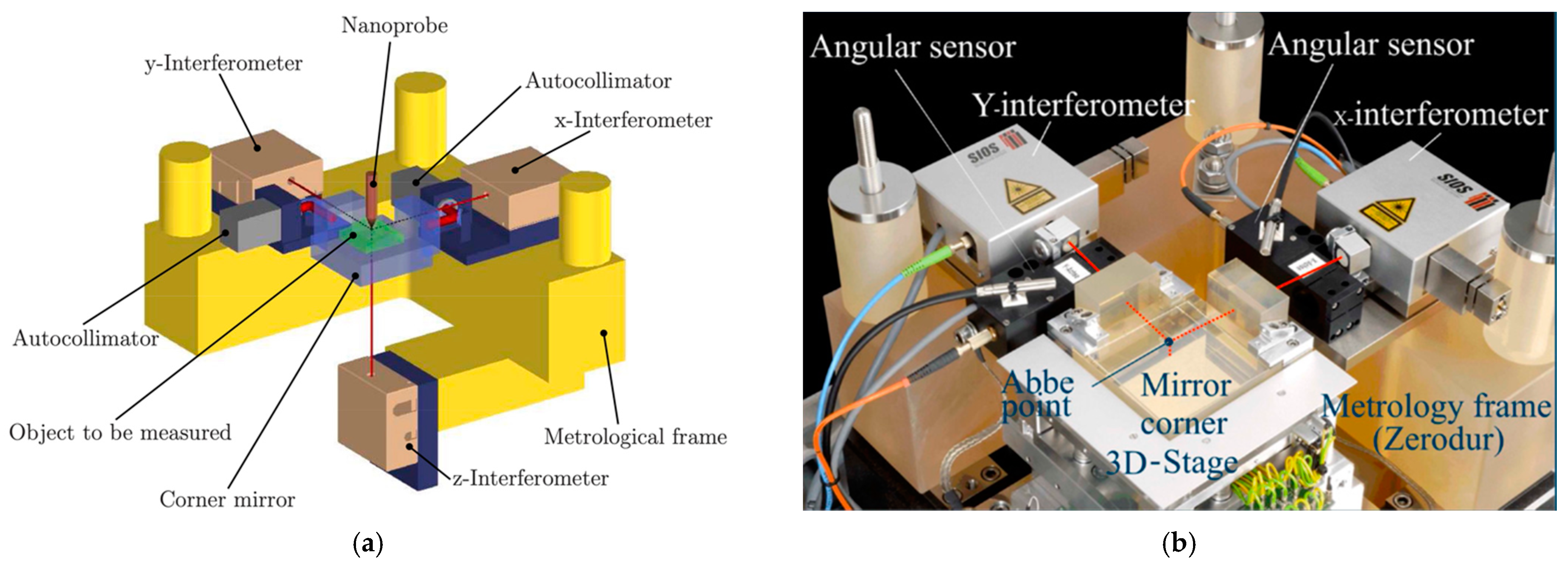
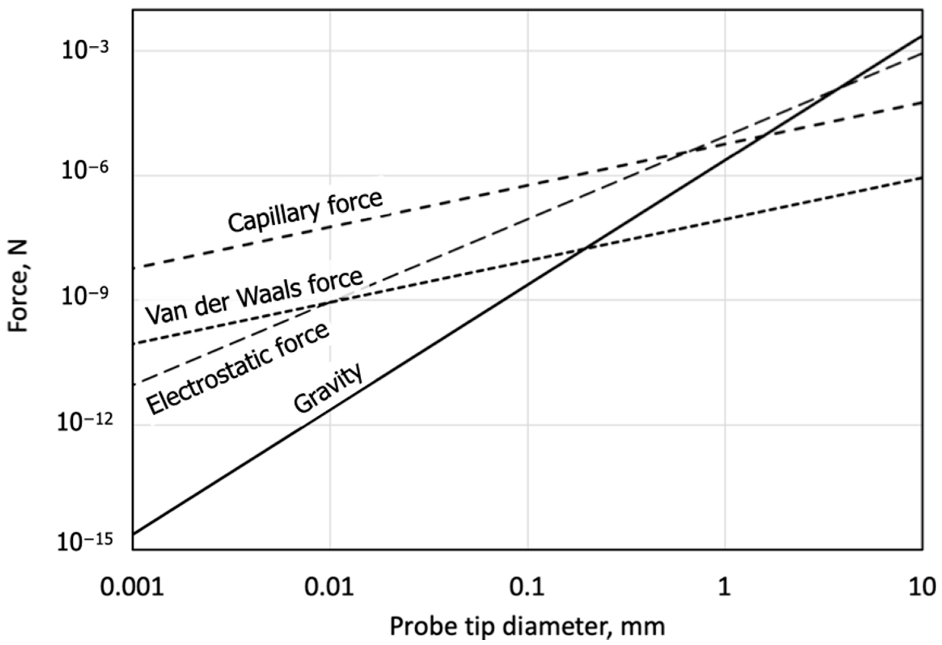
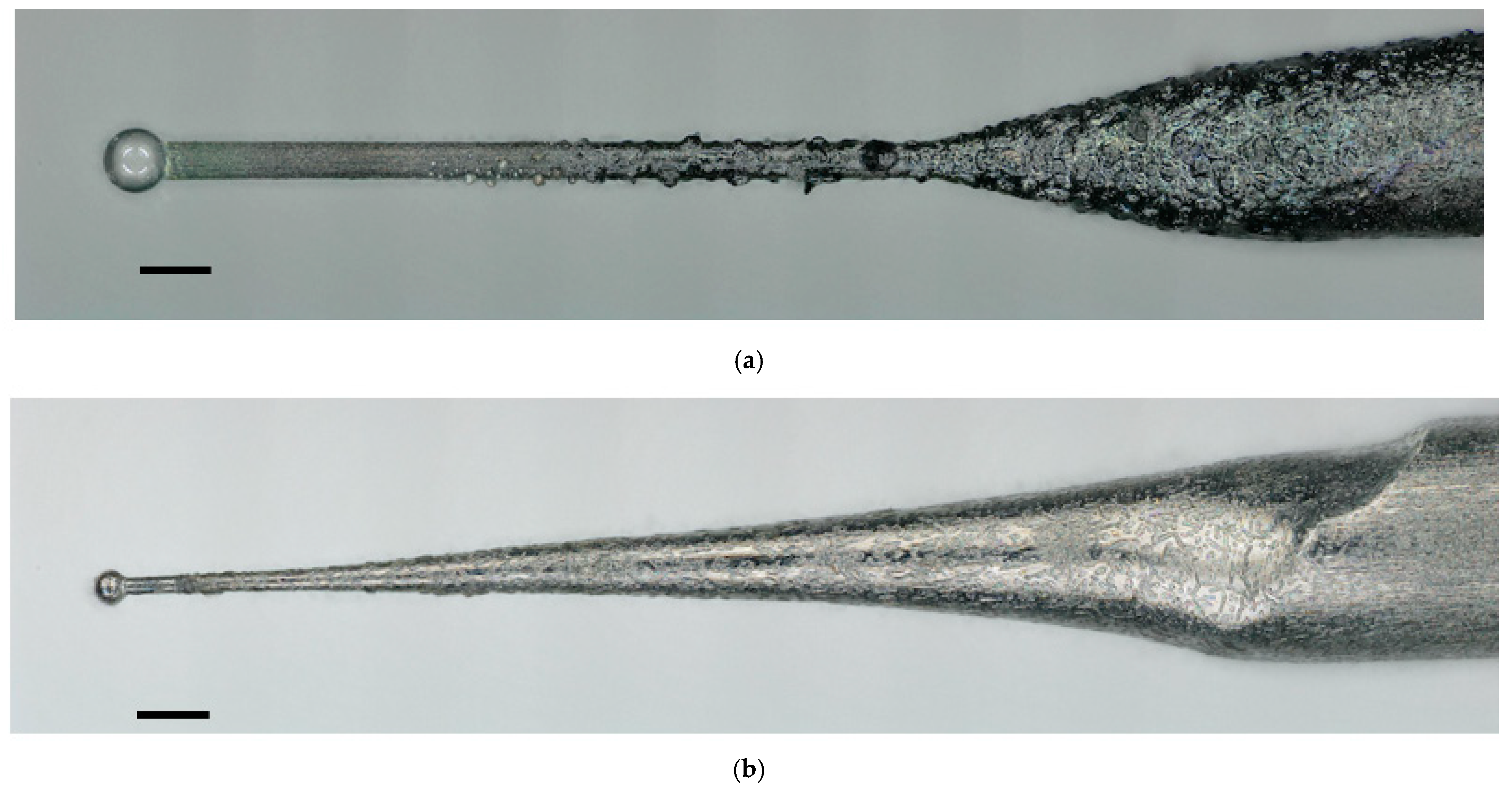
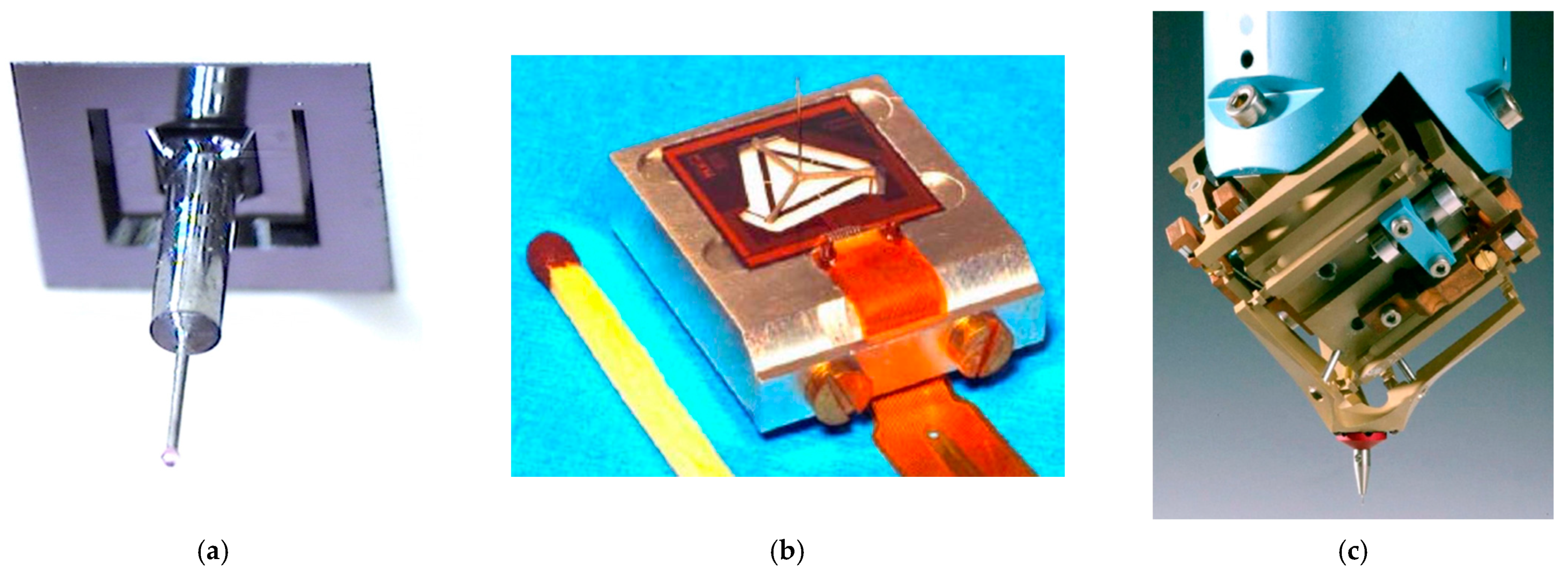
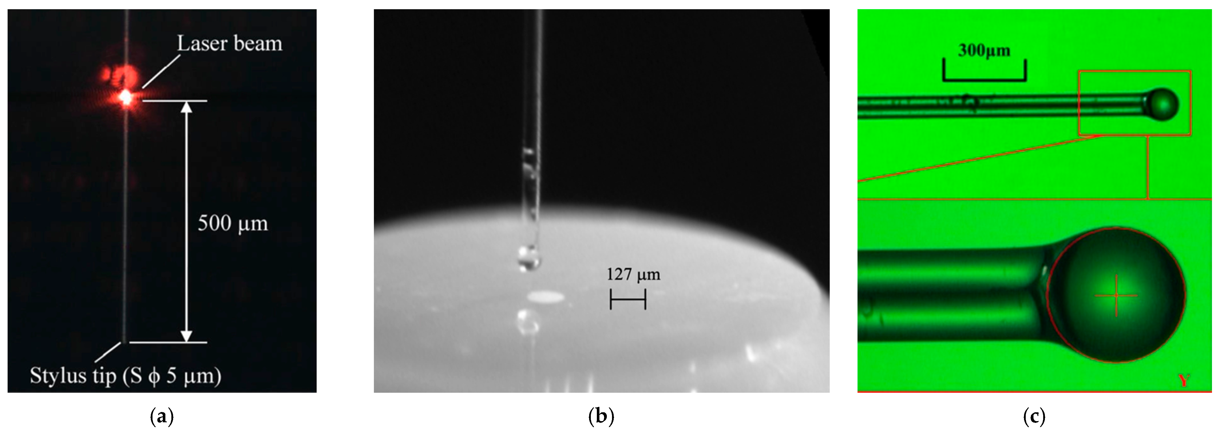
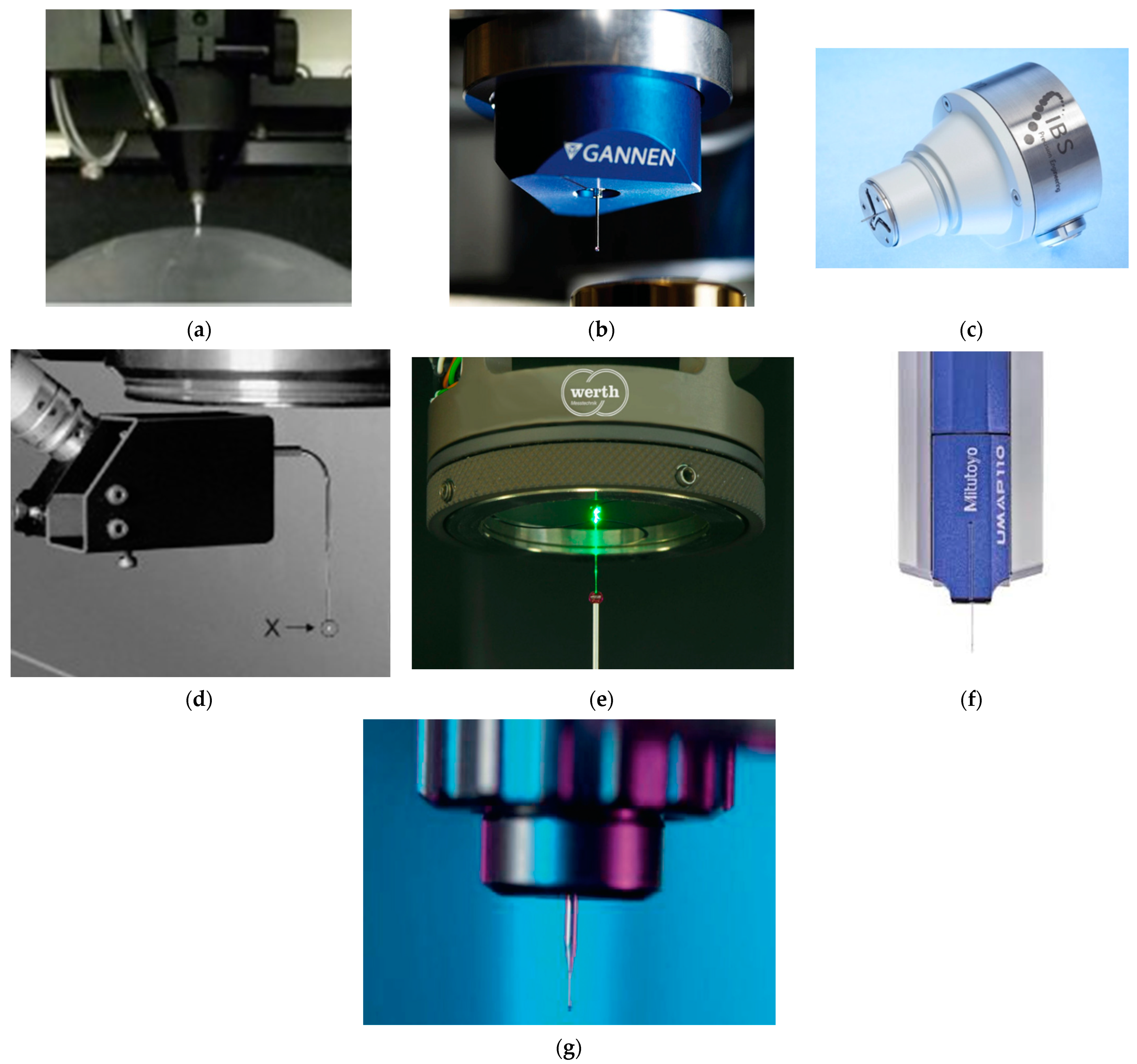
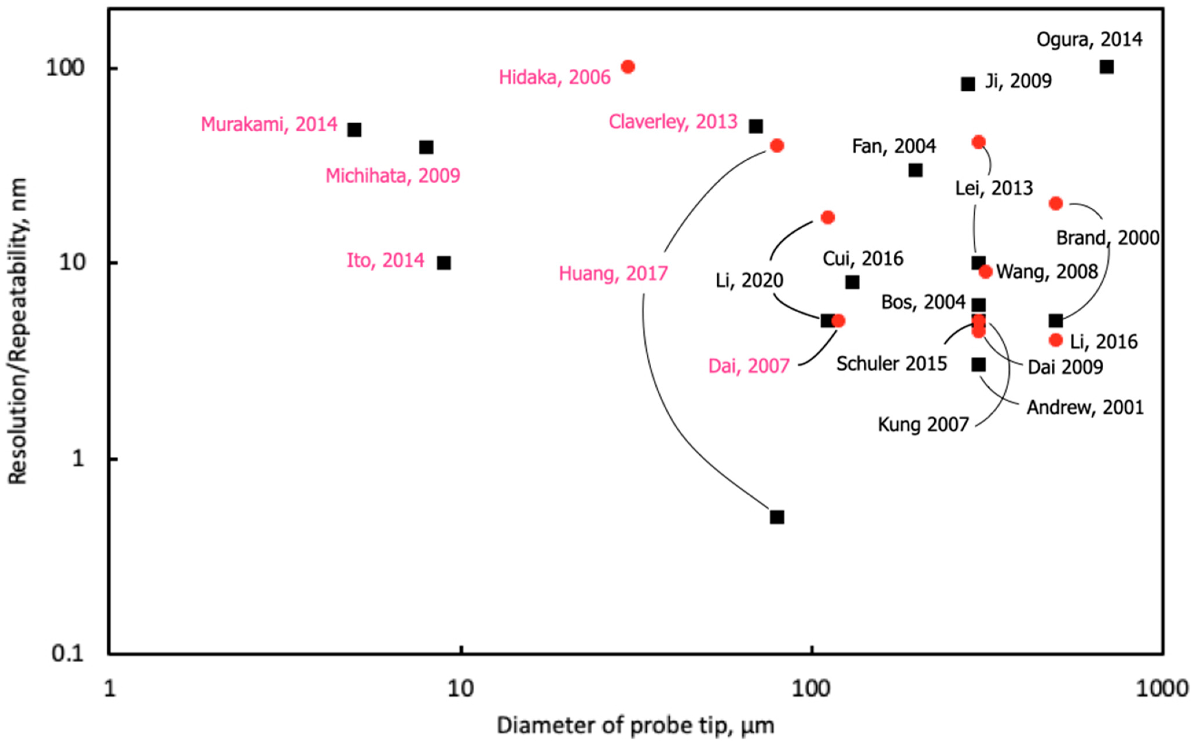
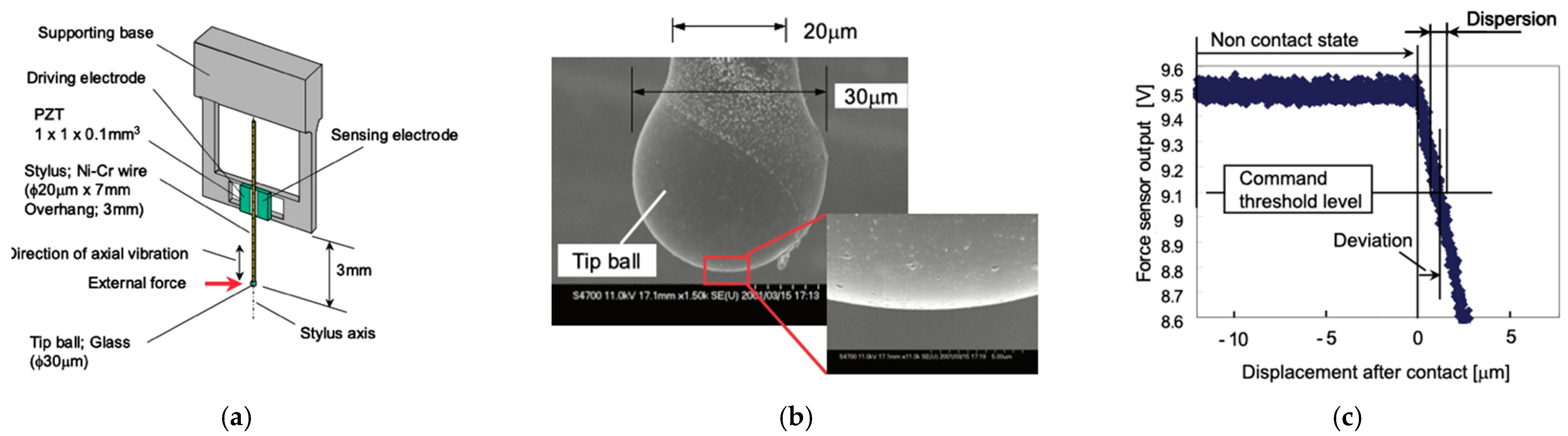
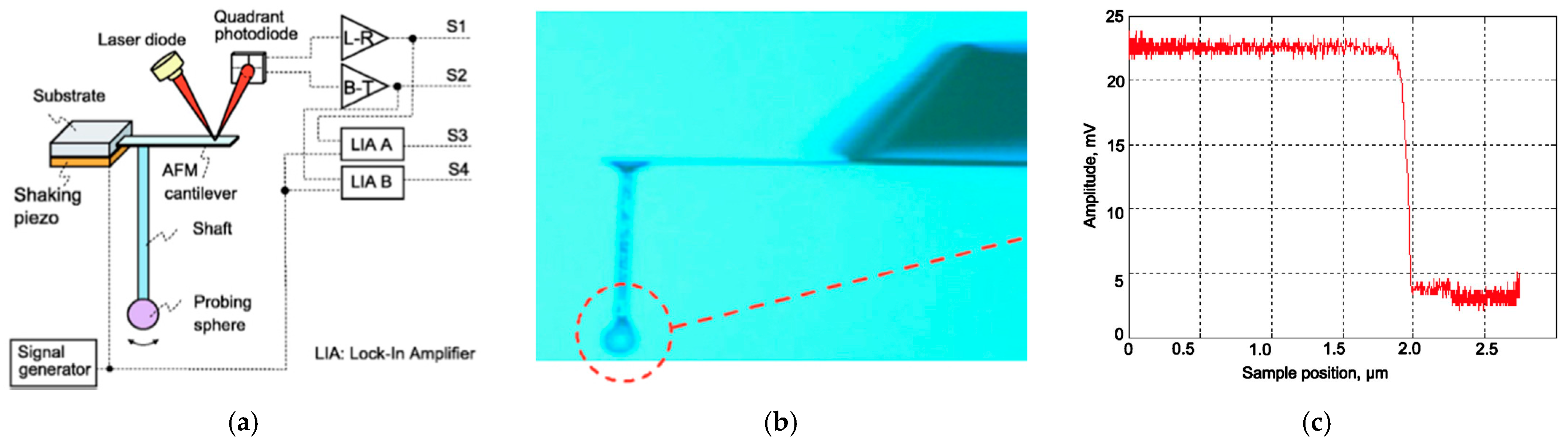
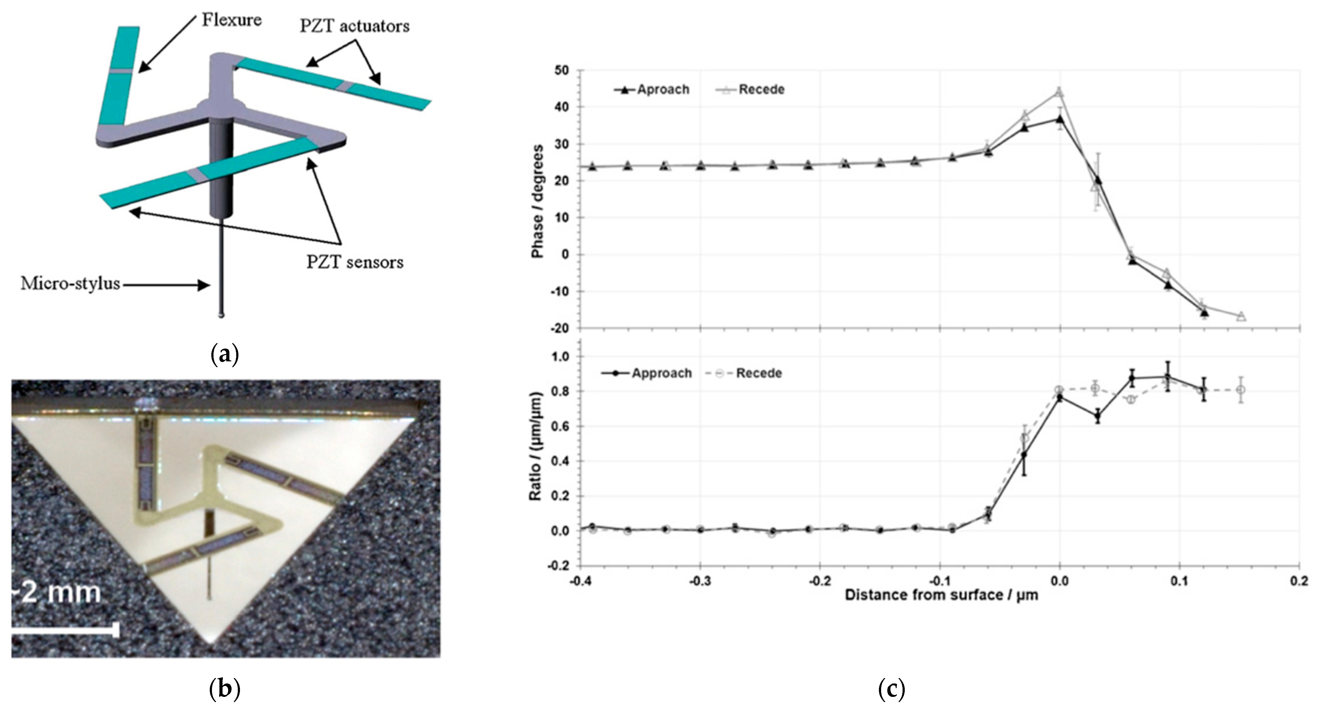
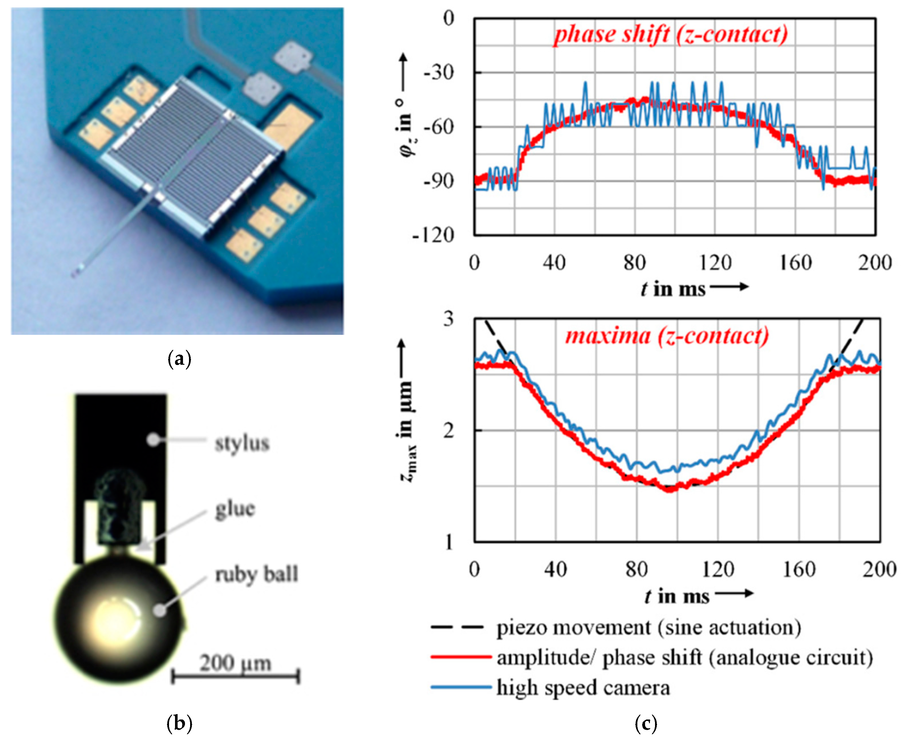
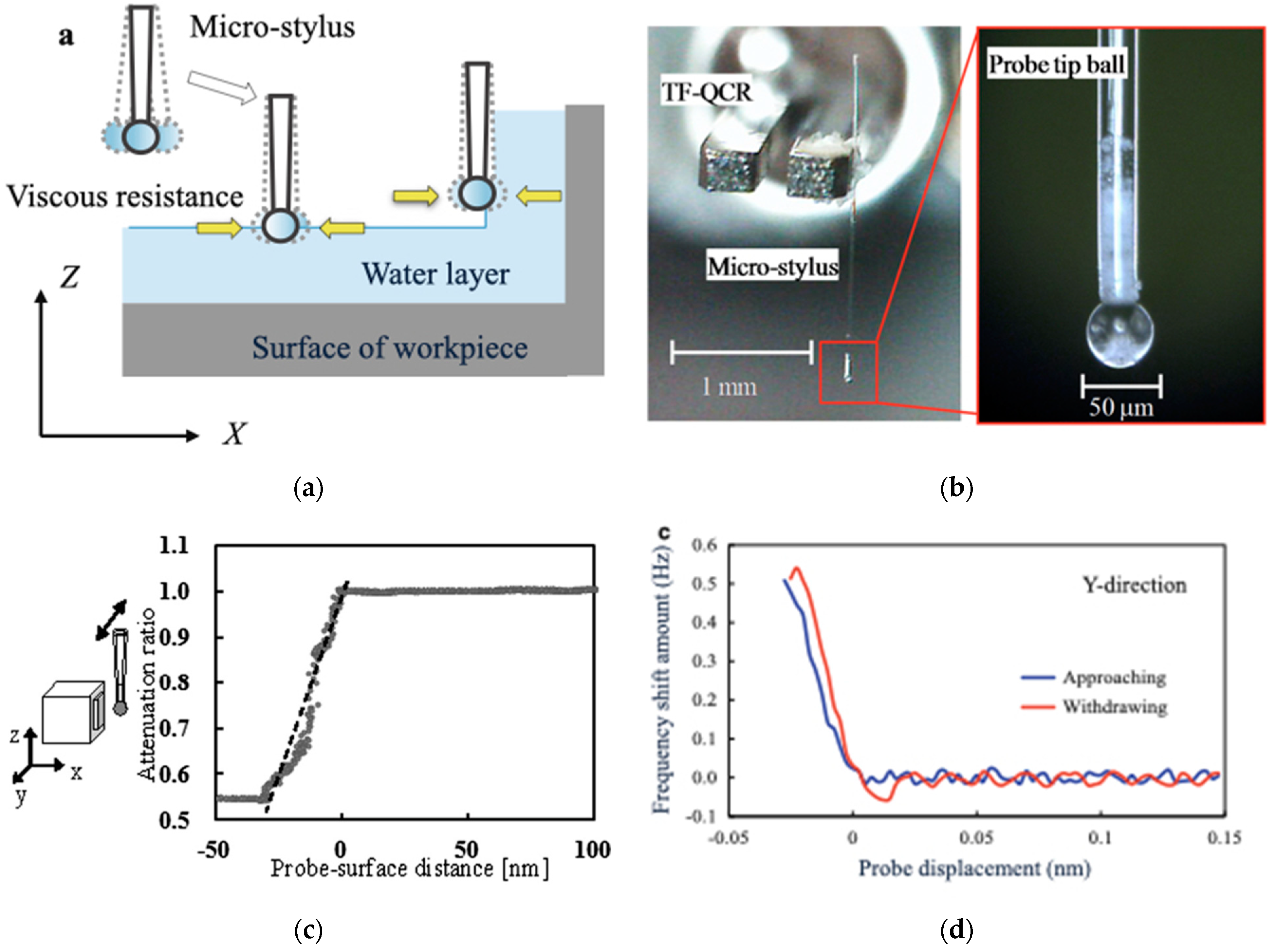
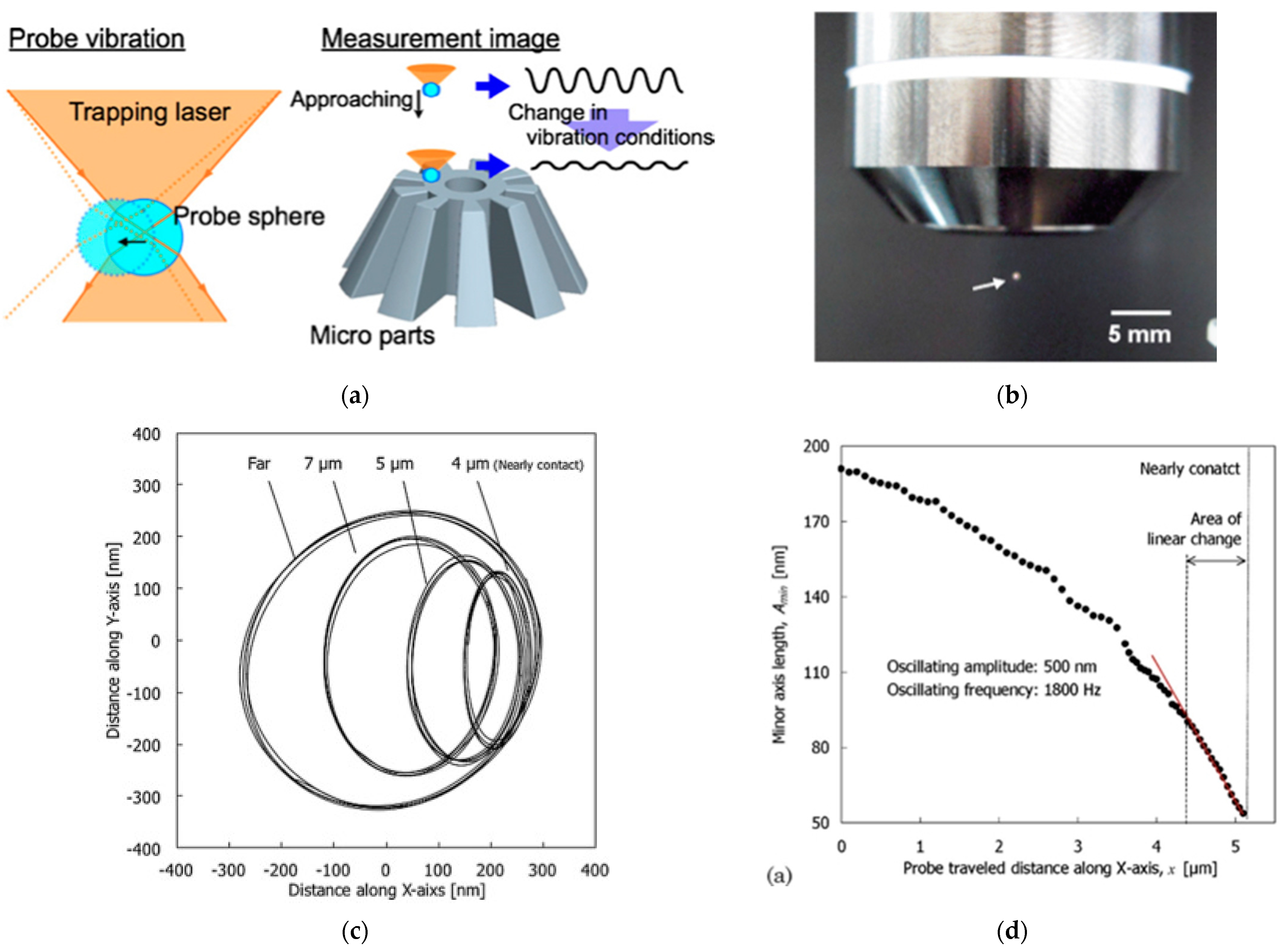
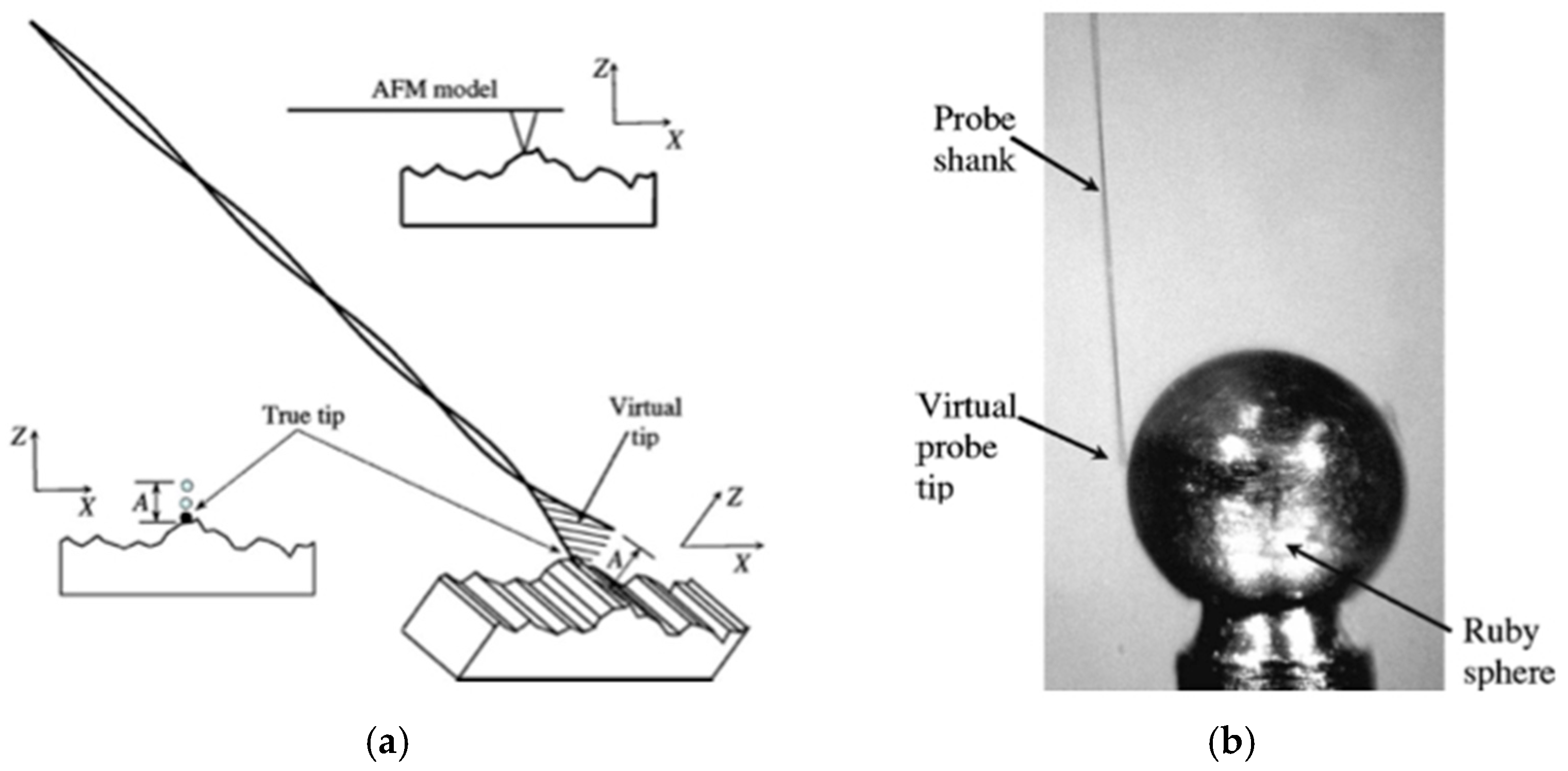
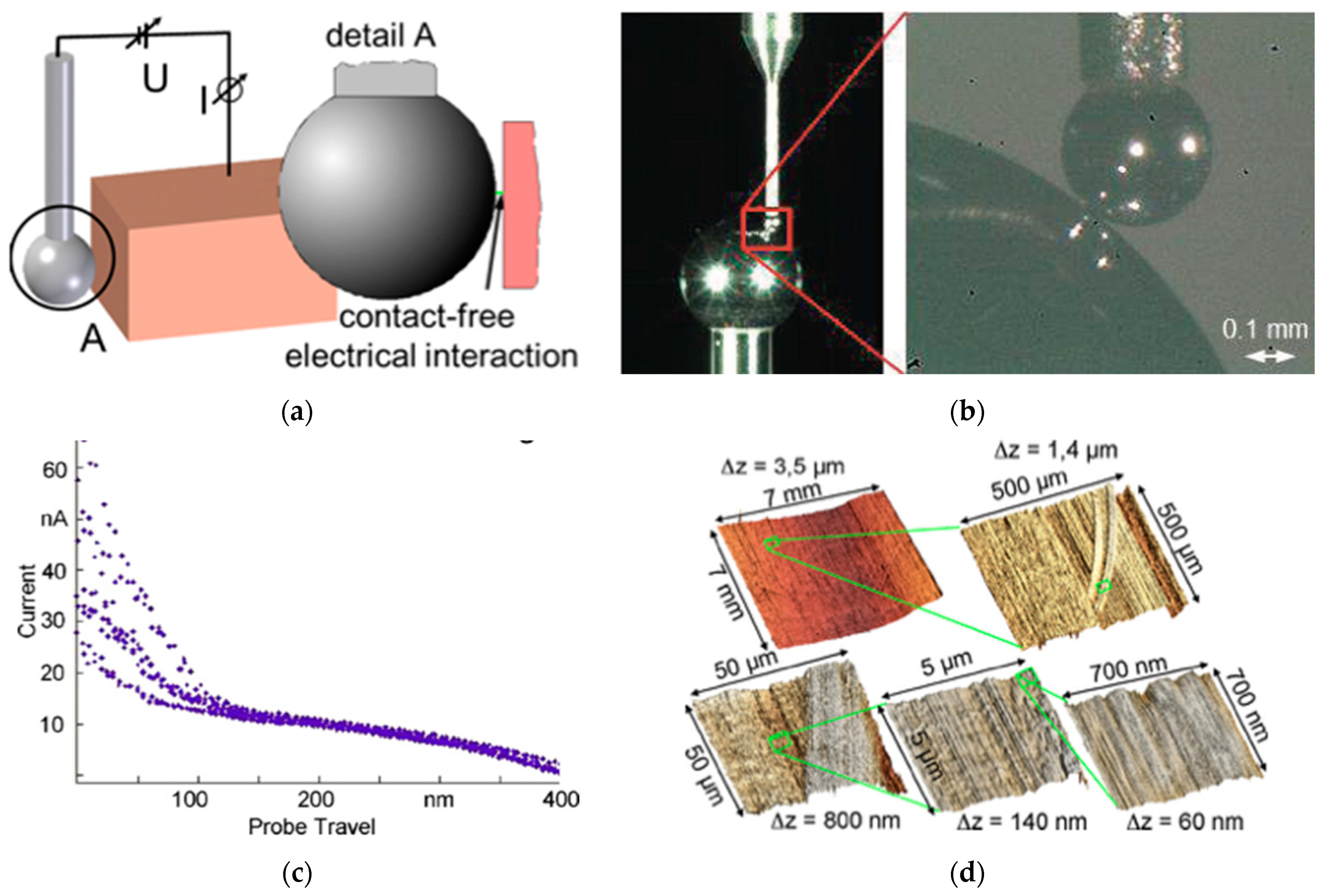
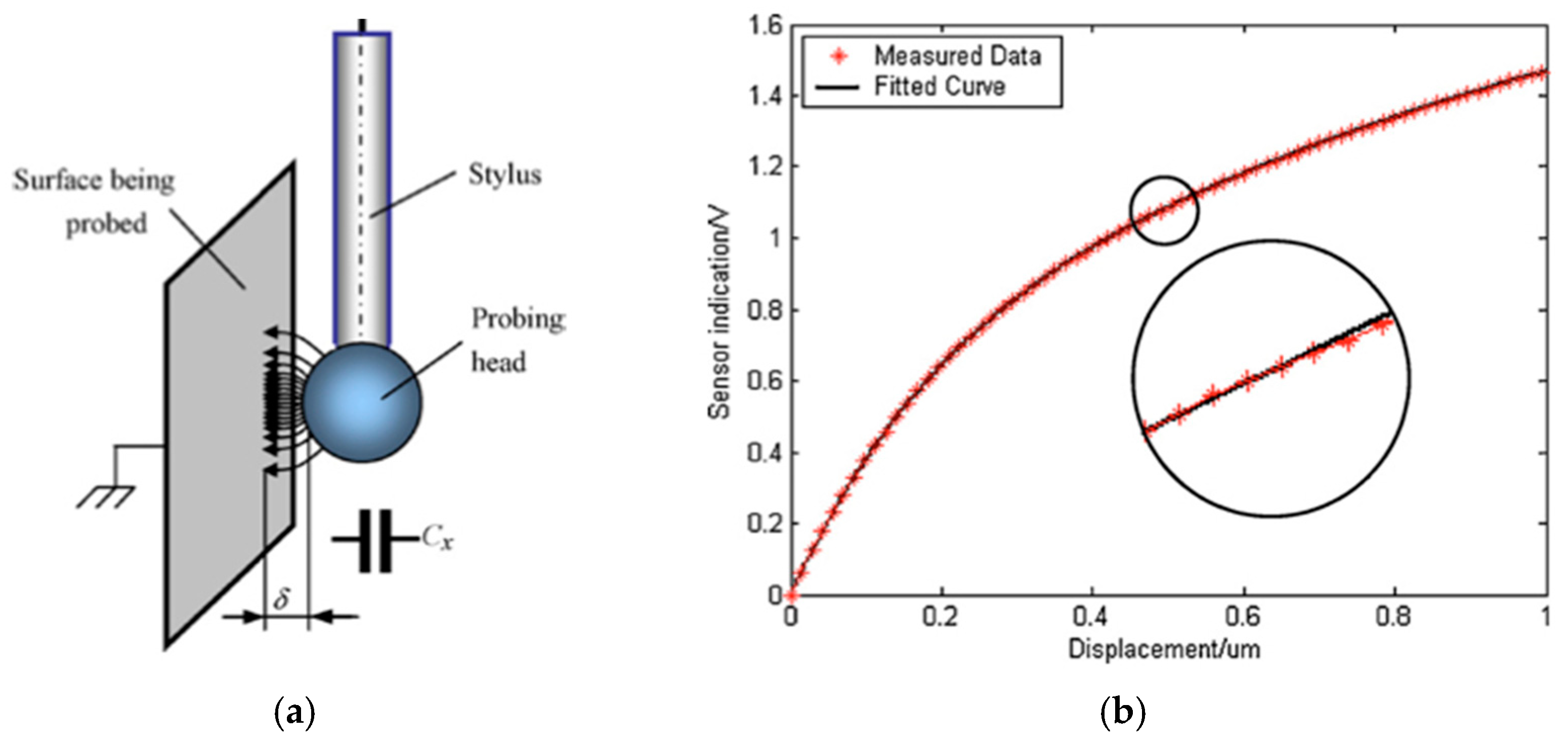
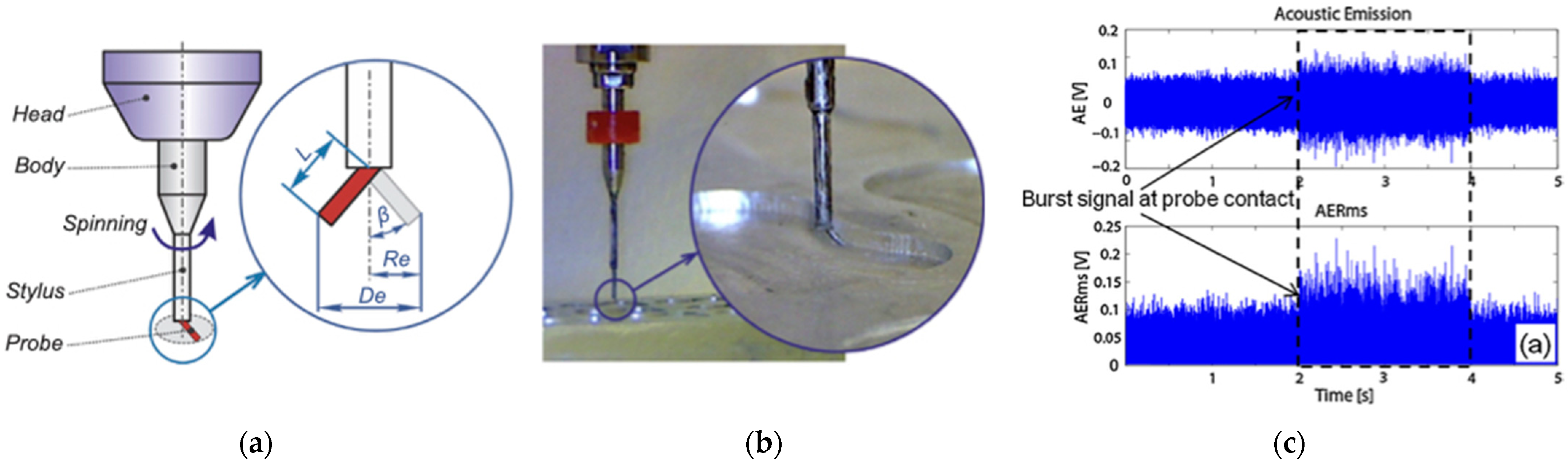
Table 1.
The required specifications of micro-CMMs in [10].
Table 1.
The required specifications of micro-CMMs in [10].
| Conventional CMM | micro-CMM | |
|---|---|---|
| Measuring range | (1 m)3 | (10 mm)3 |
| Resolution | 1 μm | 10 nm |
| Accuracy | 5 μm | 50 nm |
| Probe tip size | 5 mm | 50 μm |
| Measuring force | 10−1 N | 10−3 N |
Table 2.
Summary of the commercialized microprobe systems.
| Sensing Principle | Probe Tip Diameter | Shaft Length | Probing Force | Probe Tip Material | |
|---|---|---|---|---|---|
| Panasonic, UA3P-AFP | Contact, Hinge-type probe | 30, 80 μm | 300, 500 μm | 0.3 mN | Ruby, Tungsten carbide |
| Xpress PE, GANNEN XP | Contact, Hinge-type Vibration probe | 50–120 μm | 6.8 mm | 0.4 mN | Ruby |
| IBS P.E. Trislelion | Contact, Hinge-type probe | 80–250 μm | 6–8.5 mm | 0.3 mN | Ruby |
| 3D Werth Fiber Probe | Contact, Fiber probe | 40–250 μm | 20 mm | 1–100 μN | Glass |
| Werth Fiber Probe, WFP/S | Contact, Fiber probe | down to 25 μm | 150 mm | 1–100 μN | Glass |
| Mitutoyo, UMAP | Vibration probe | 15–300 μm | 0.2–16 mm | 1–25 μN | Glass |
| Zeiss, F25 probe | Contact, Hinge-type probe | 100–700 μm | up to 4 mm | 0.5 mN | Ruby |
Table 3.
Summary of the vibration-based microprobe.
| Probe Tip Diameter | Shaft Length | Aspect Ratio | Probing Force | Resonant Frequency | Stiffness | Respond Distance † | |
|---|---|---|---|---|---|---|---|
| UMAP | 30 μm | 3 mm | 100 | 0.15 μN | 349 kHz | − | non |
| ACP | 120 μm | 1 mm | 8 | 1 μN | 260 kHz | 15 N/m | 200–300 nm |
| Vibrating tactile probe | 70 μm | 1 mm | 14 | − | 1.6 kHz | 15 N/m | 100 nm |
| Resonant probe | 200 μm | 4 mm | 20 | − | 0.73 kHz | 10 N/m | non |
| Share force detection probe | 50 μm | 2.5 mm | 50 | − | − | − | 30 nm |
| Resonant triggering probe | 80 μm | 1 mm | 12.5 | μN order | 32 kHz | 143 N/m | A few nm |
| Laser-trapping-based probe | 8 μm | 30 μm | 4 | − | 2.7 kHz | 1.5 × 10⁻⁴ N/m | 10 μm |
† Respond distance means the distance from the measurement surface where the probe response signal begins to be detected.
Publisher’s Note: MDPI stays neutral with regard to jurisdictional claims in published maps and institutional affiliations. |
© 2022 by the author. Licensee MDPI, Basel, Switzerland. This article is an open access article distributed under the terms and conditions of the Creative Commons Attribution (CC BY) license (https://creativecommons.org/licenses/by/4.0/).
Share and Cite
MDPI and ACS Style
Michihata, M. Surface-Sensing Principle of Microprobe System for Micro-Scale Coordinate Metrology: A Review. Metrology 2022, 2, 46-72. https://doi.org/10.3390/metrology2010004
AMA Style
Michihata M. Surface-Sensing Principle of Microprobe System for Micro-Scale Coordinate Metrology: A Review. Metrology. 2022; 2(1):46-72. https://doi.org/10.3390/metrology2010004
Chicago/Turabian StyleMichihata, Masaki. 2022. "Surface-Sensing Principle of Microprobe System for Micro-Scale Coordinate Metrology: A Review" Metrology 2, no. 1: 46-72. https://doi.org/10.3390/metrology2010004