
Characterization of Thin AlN/Ag/AlN-Reflector Stacks on Glass Substrates for MEMS Applications

 ,
,  and
and
Abstract
:1. Introduction
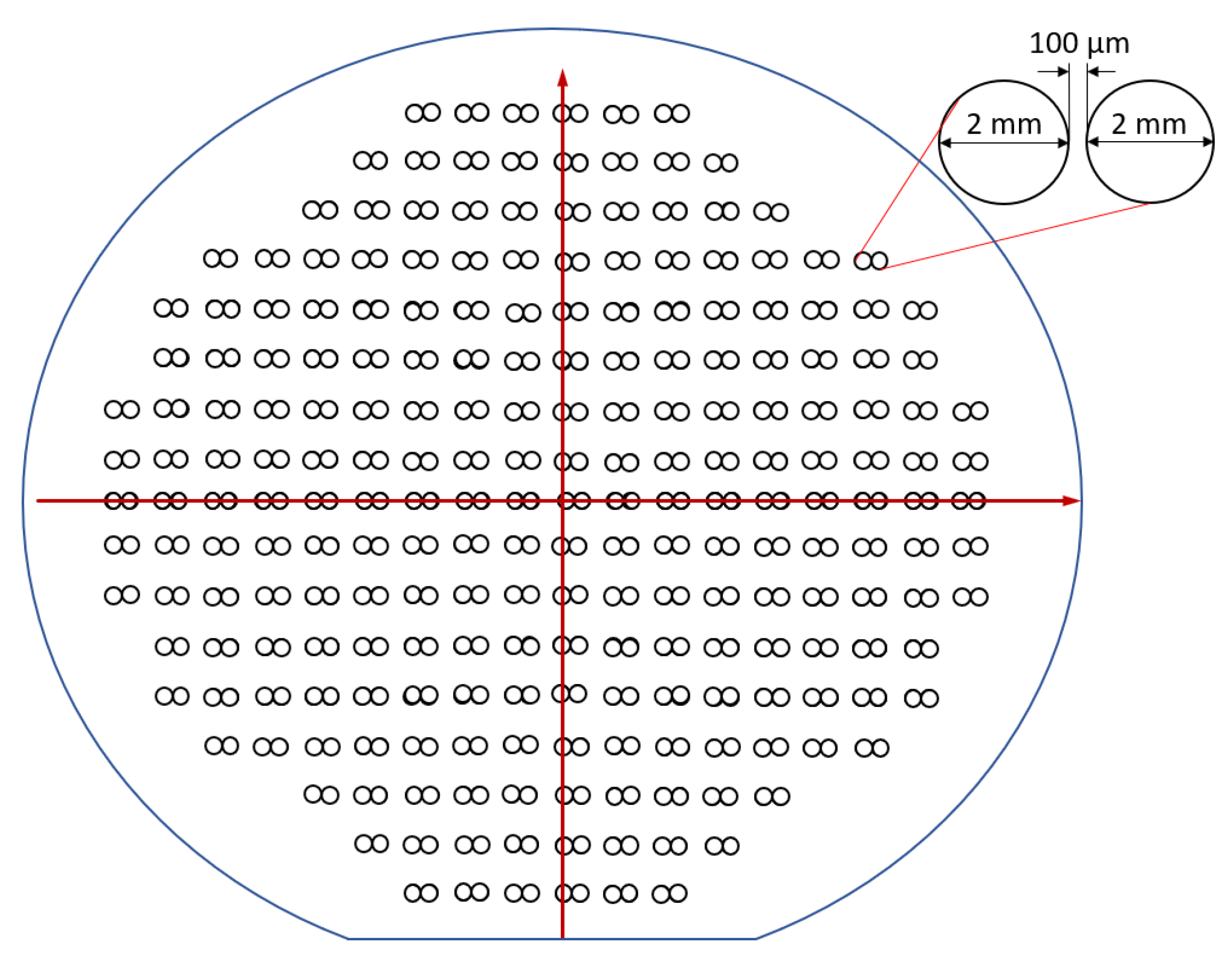
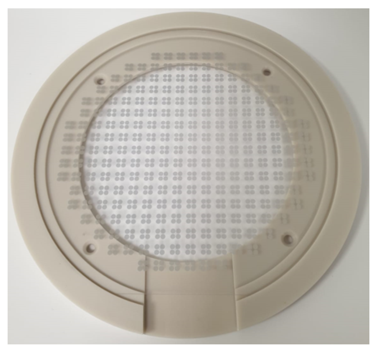
2. Fabrication and Inline Characterization of Reflectors
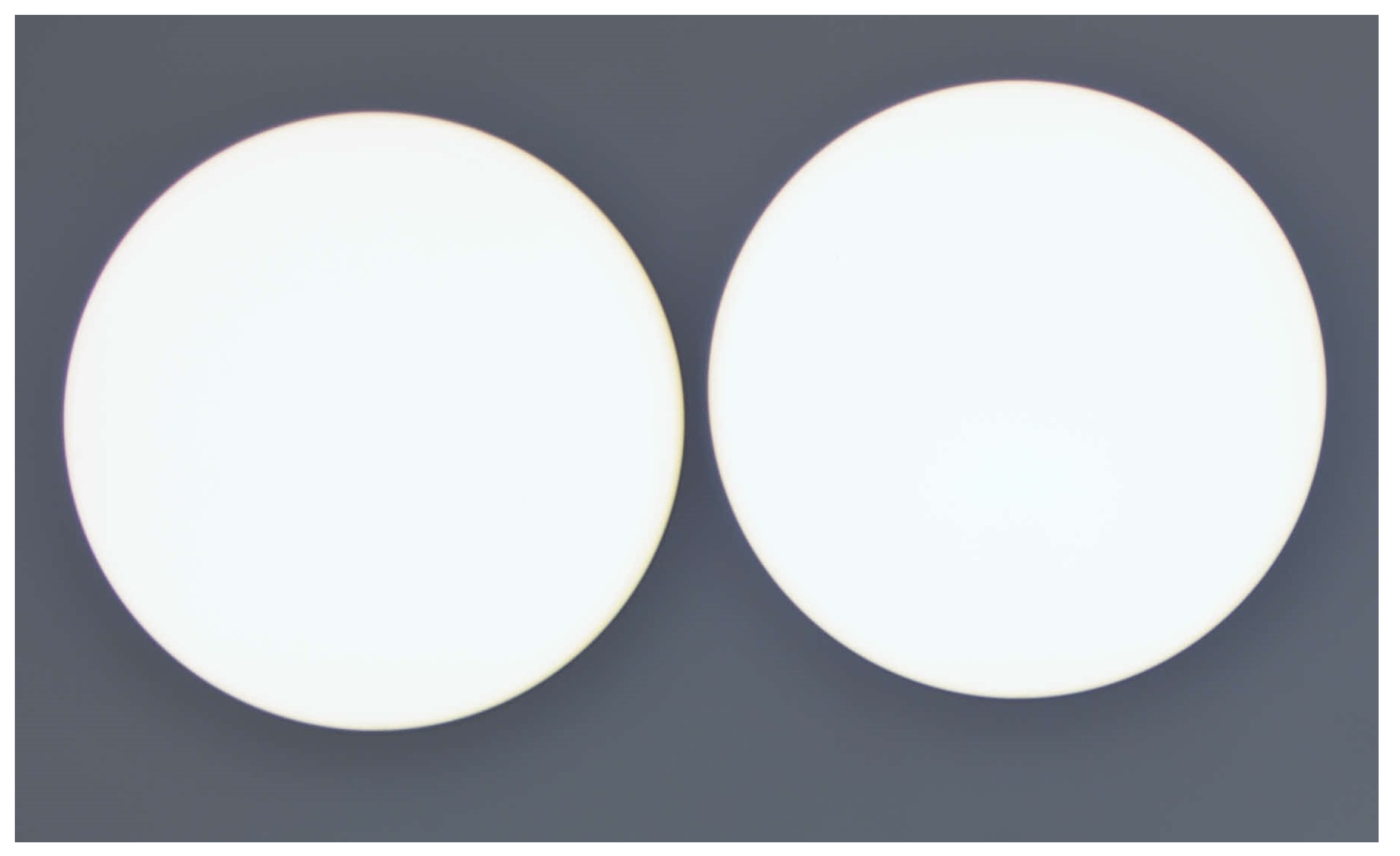
2.1. Deposition of Pure Ag-Layers
2.2. Structuring of Pure Ag-Reflectors and AlN/Ag/AlN-Reflector Stacks
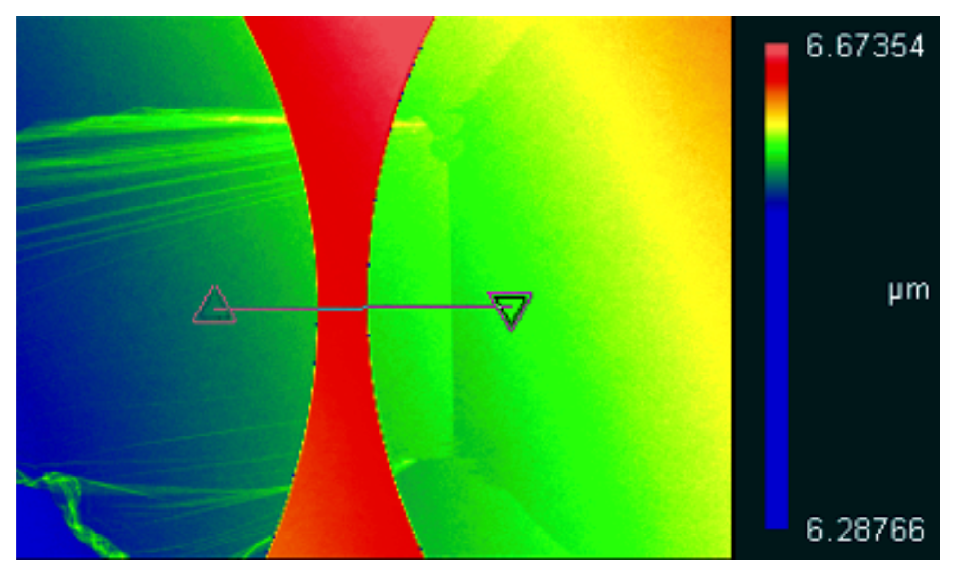
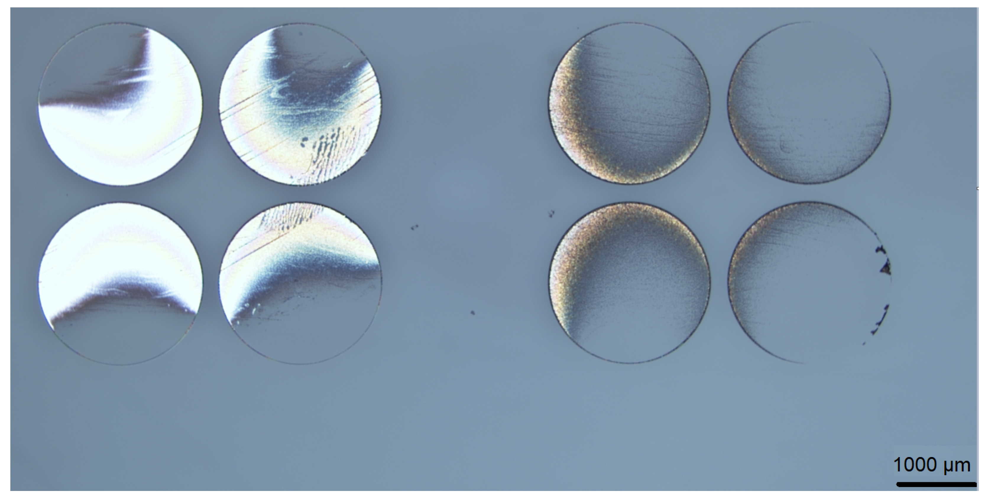
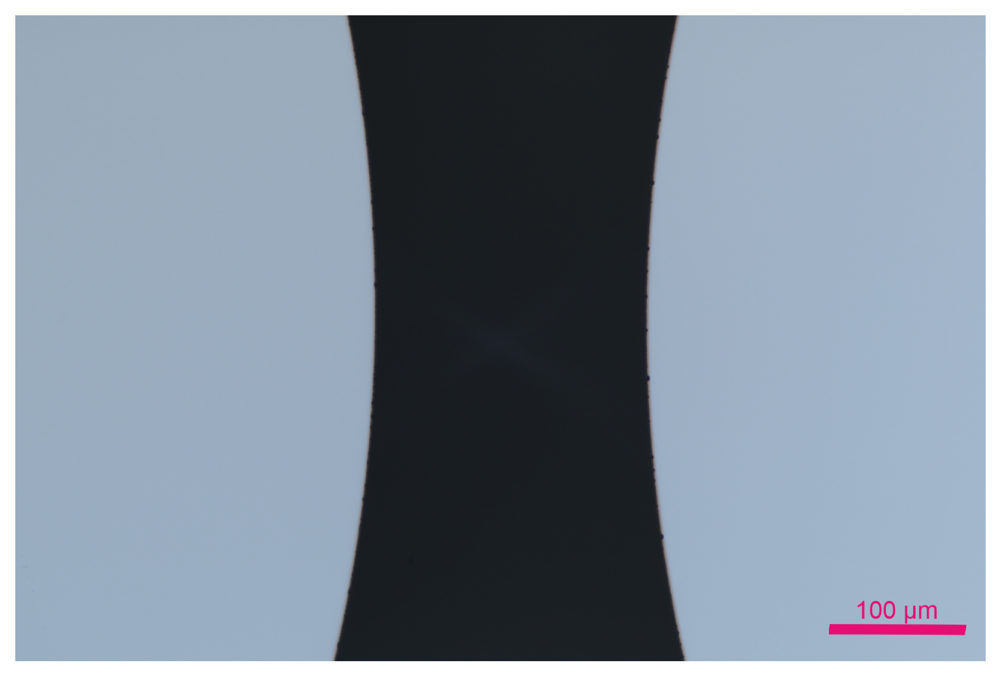
2.2.1. Wet Etch
2.2.2. Dry Etch
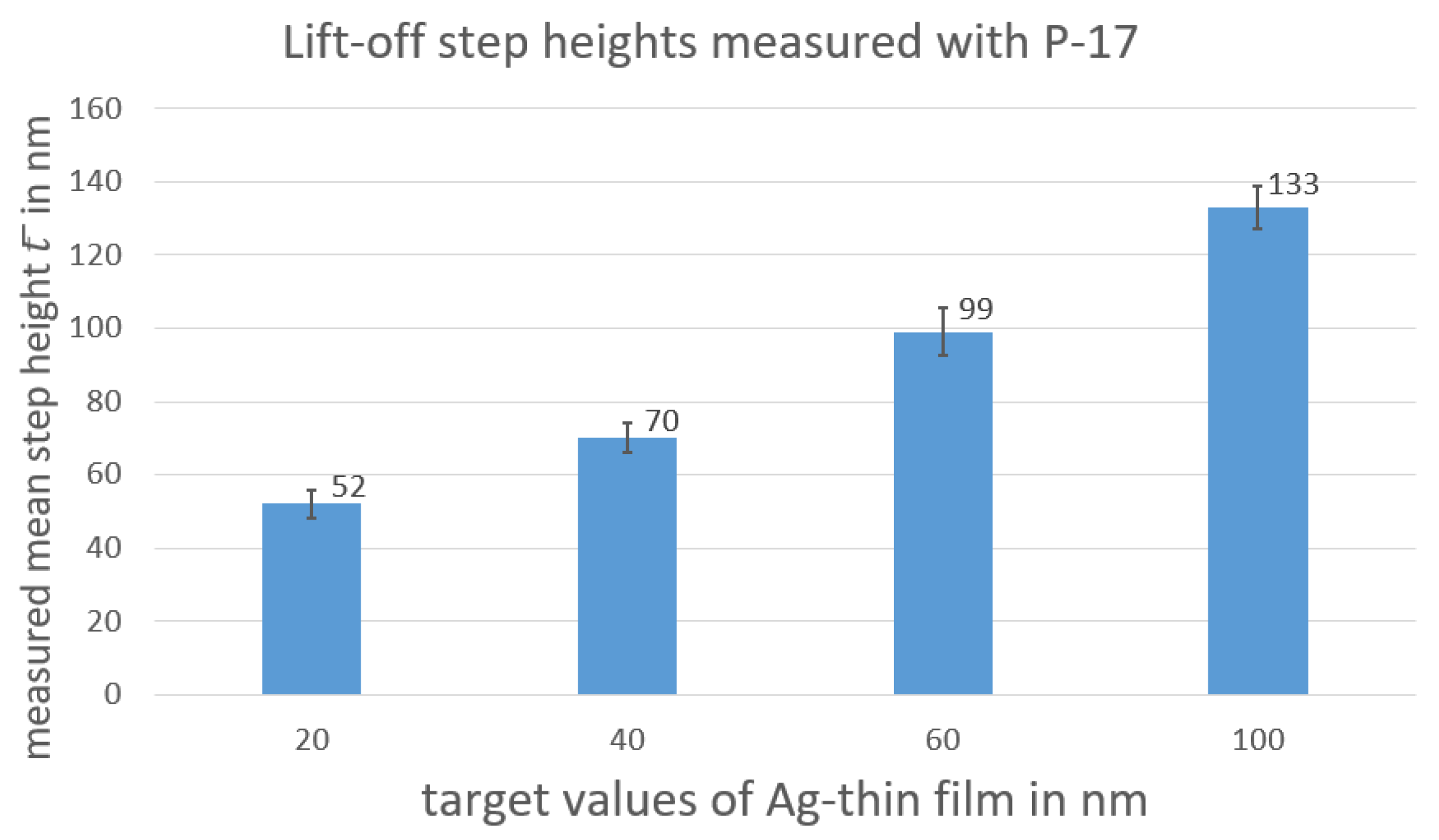
2.2.3. Lift-Off
2.3. Summary
3. Optical Characterization
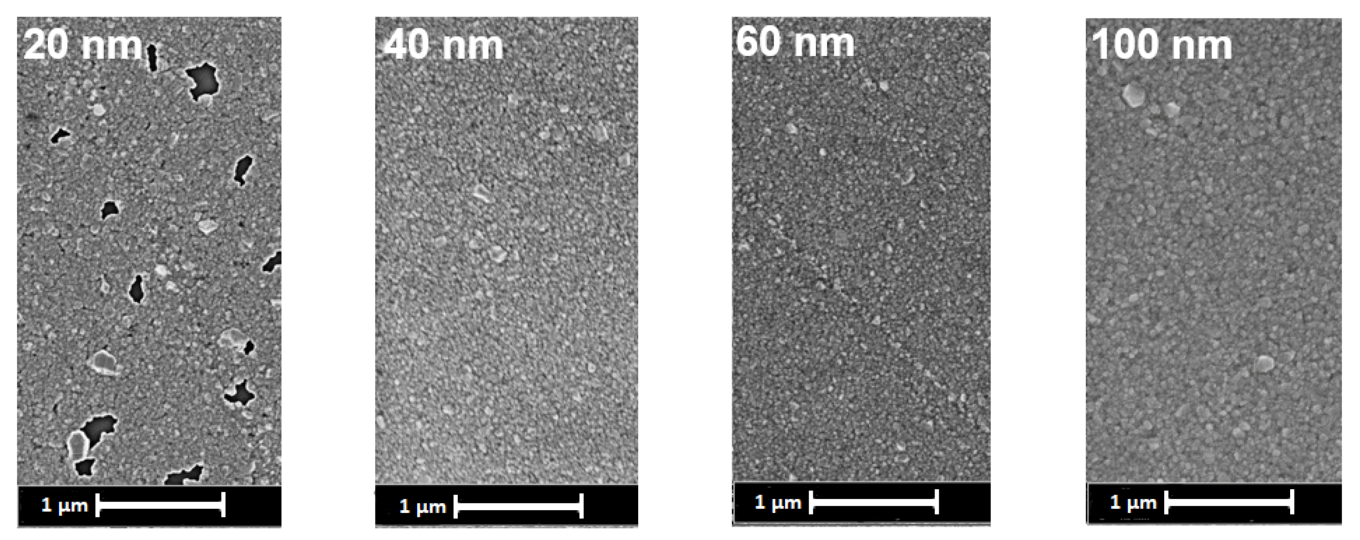
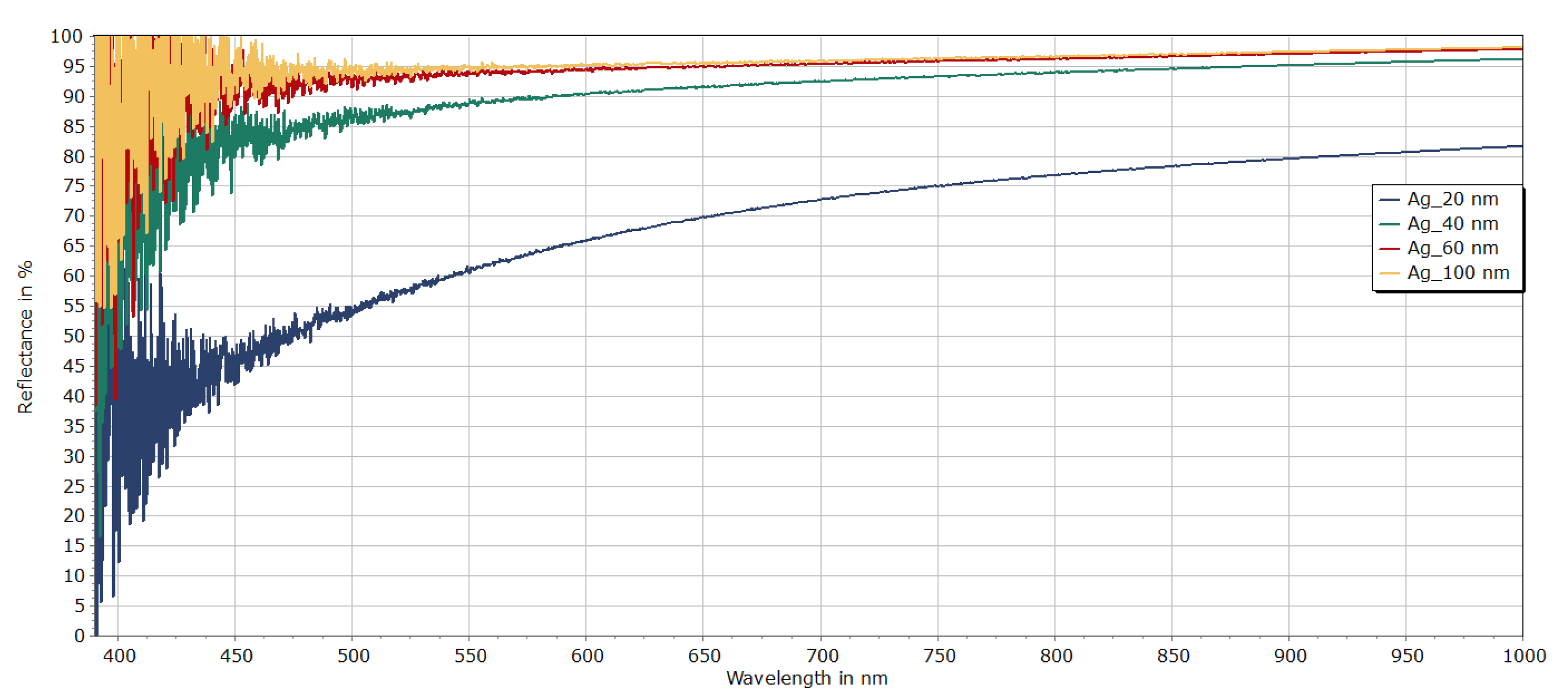
3.1. Optical Characterization of Pure Ag-Reflectors
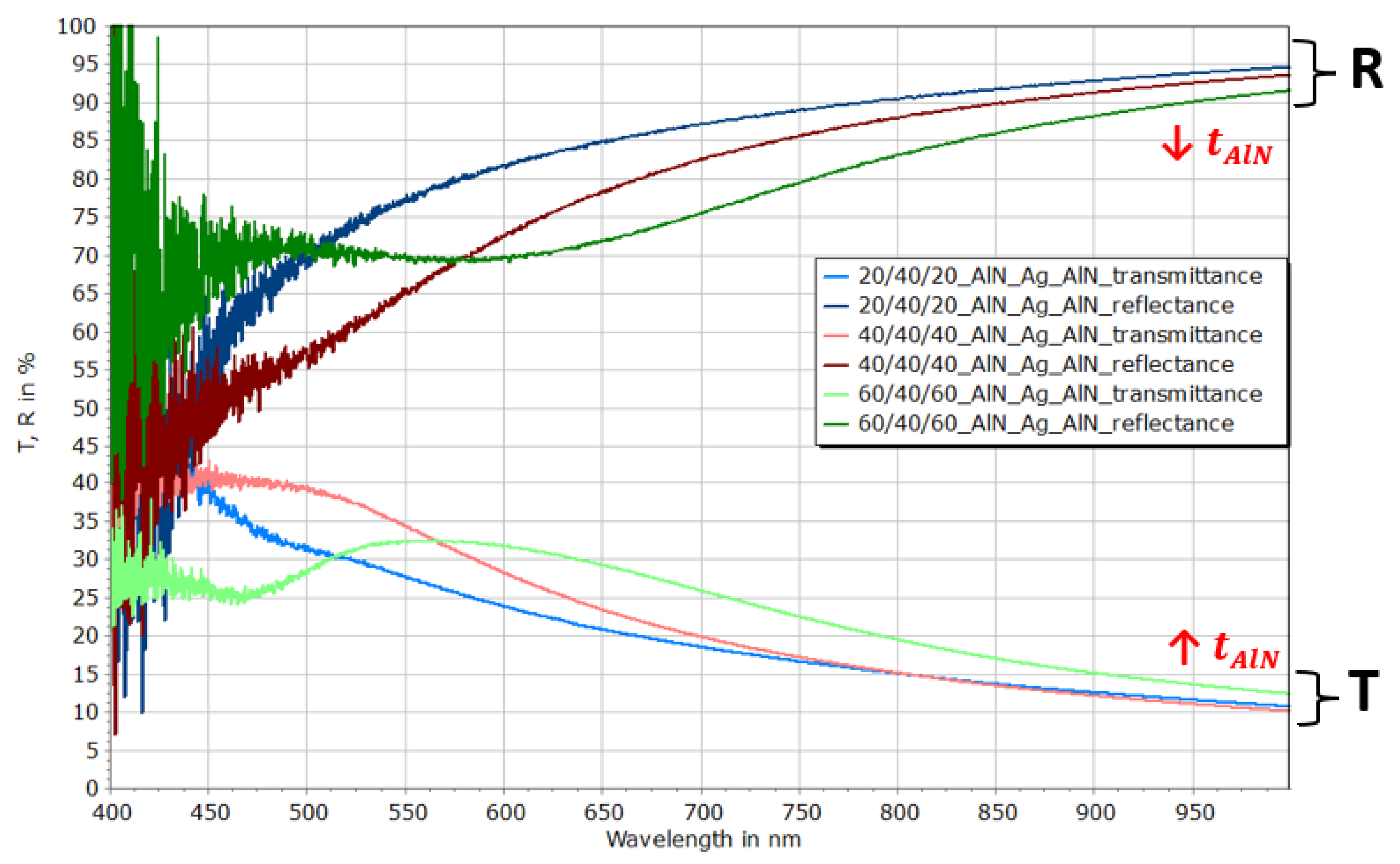
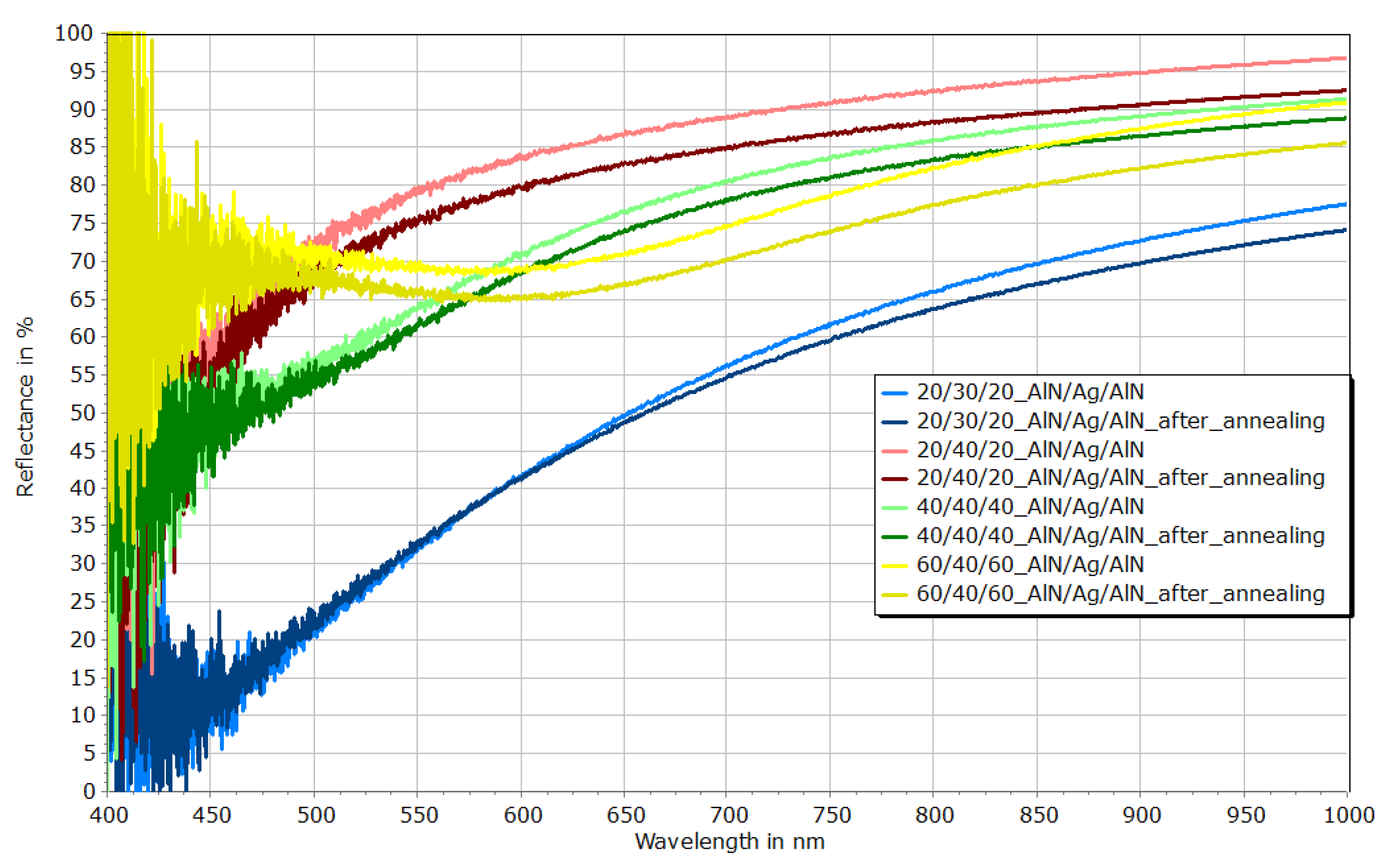
3.2. Characterization of AlN/Ag/AlN-Reflector Stacks in VIS
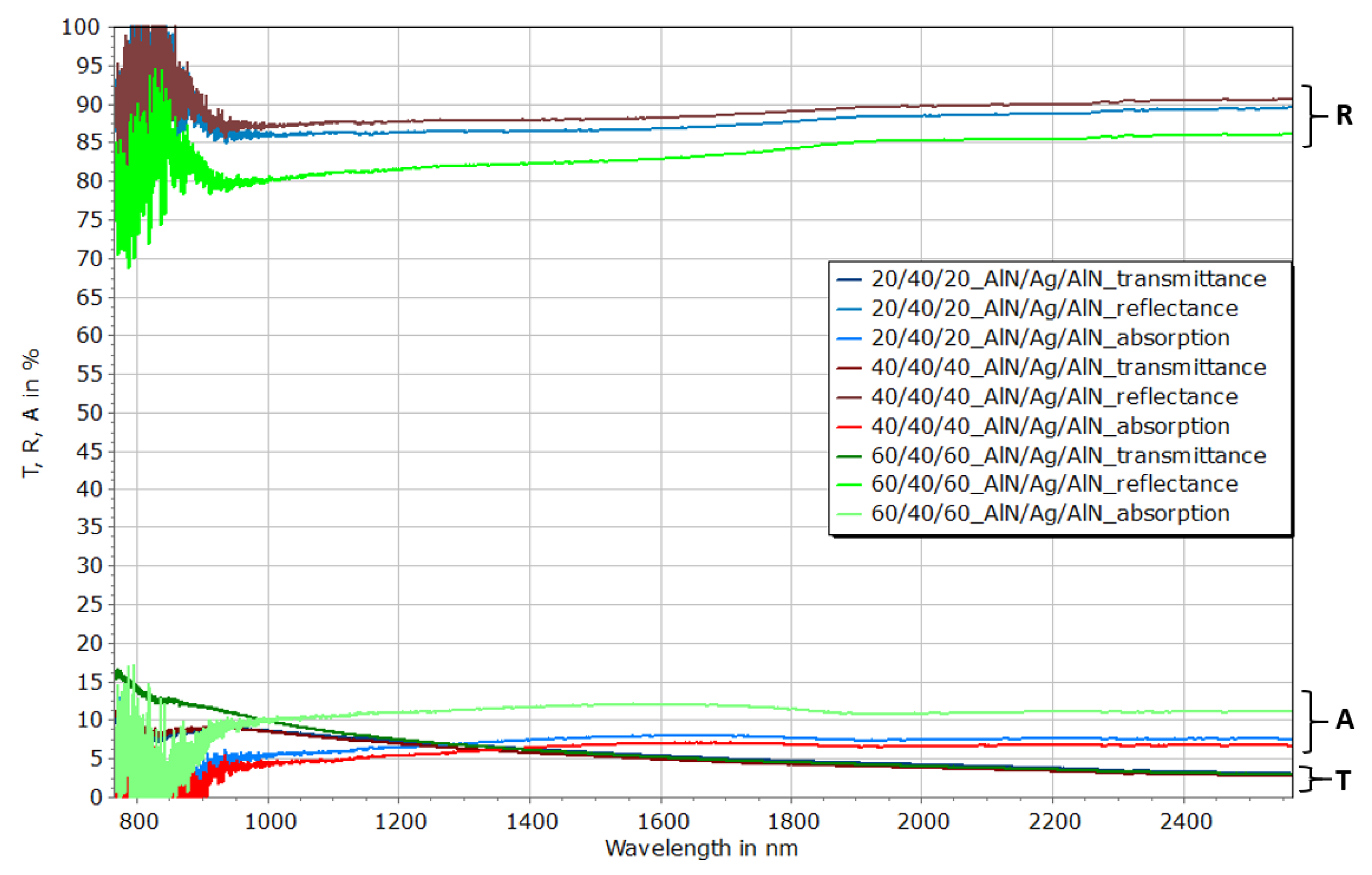
3.3. NIR
3.4. Annealing
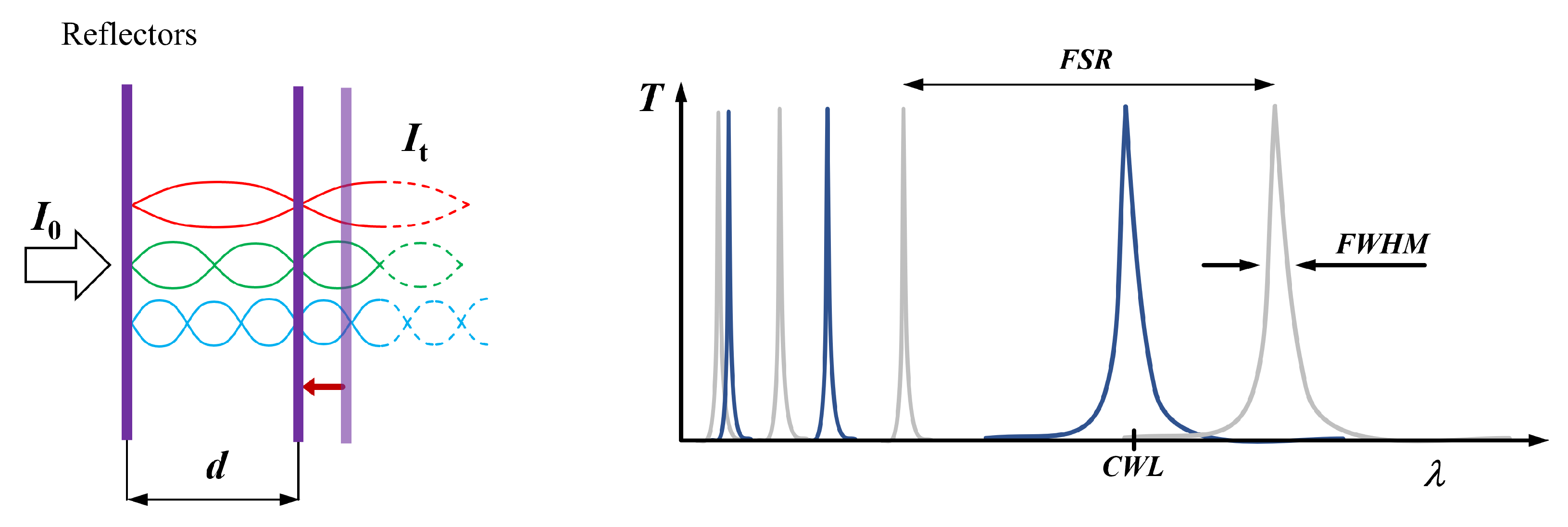
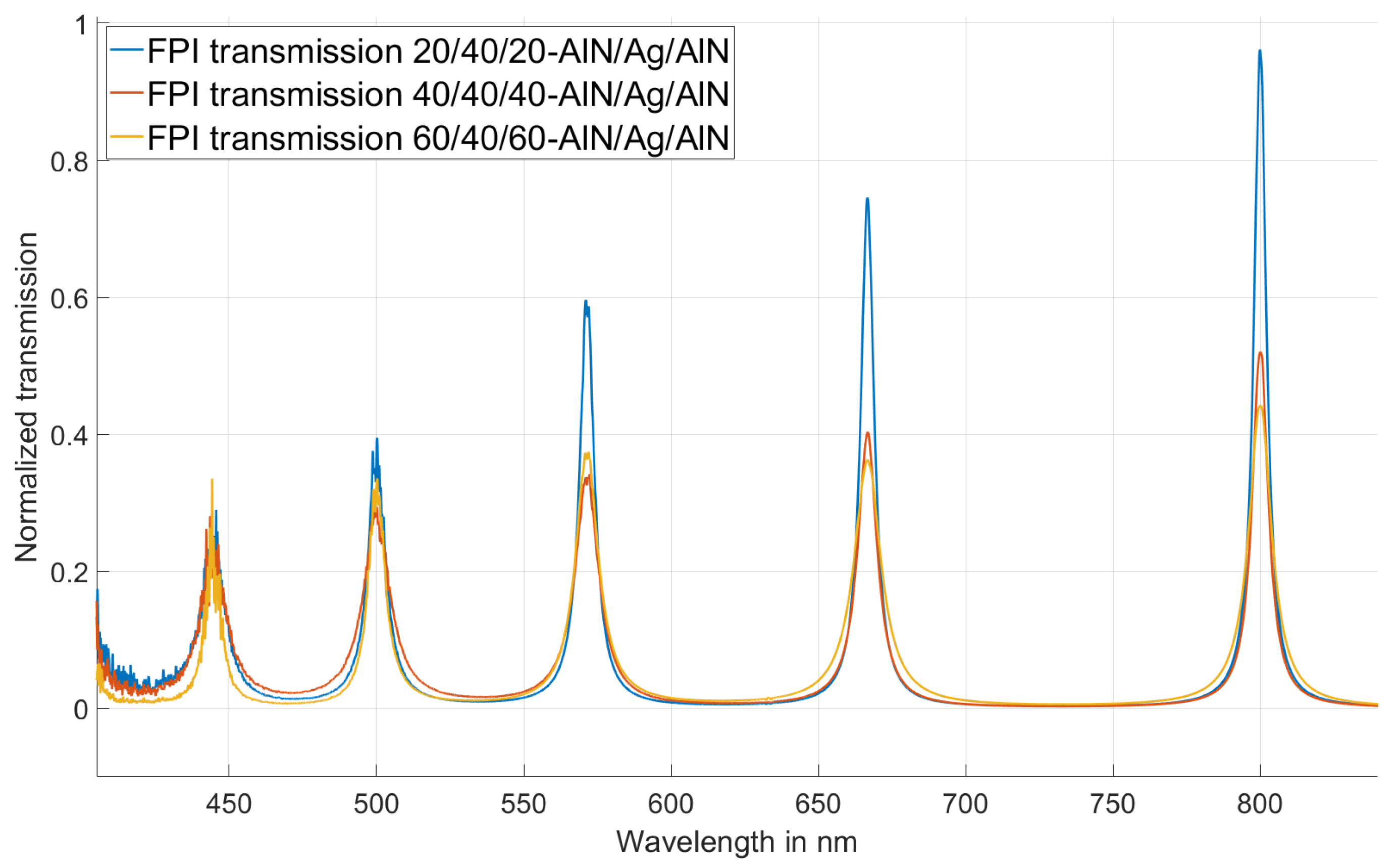
4. Application of Fabricated Reflectors for FPI
5. Conclusions
Author Contributions
Funding
Data Availability Statement
Acknowledgments
Conflicts of Interest
References
- Crocombe, R.A. Portable Spectroscopy. Appl. Spectrosc. 2018, 72, 1701–1751. [Google Scholar] [CrossRef] [PubMed]
- Martyniuk, M.; Silva, K.D.; Kala, H.; Zawierta, M.; Wallace, V.P.; Walus, K.; Faraone, L.; Shadrivov, I.V. Infrared and terahertz spectrally adaptive filters based on MEMS technologies. In Proceedings of the Smart Photonic and Optoelectronic Integrated Circuits 2023, San Francisco, CA, USA, 31 January–2 February 2023; He, S., Vivien, L., Eds.; International Society for Optics and Photonics, SPIE: Bellingham, WA, USA, 2023; Volume 12425, p. 124250H. [Google Scholar] [CrossRef]
- Łabaj, F.; Kalwas, J.; Piramidowicz, R. Design and development of a miniature mid-infrared linear variable filter based spectrometer for environmental sensing. Opt. Express 2023, 31, 37583–37596. [Google Scholar] [CrossRef]
- Yang, Z.; Albrow-Owen, T.; Cai, W.; Hasan, T. Miniaturization of optical spectrometers. Science 2021, 371, eabe0722. [Google Scholar] [CrossRef] [PubMed]
- Liu, X.; Liu, W.; Ren, Z.; Ma, Y.; Dong, B.; Zhou, G.; Lee, C. Progress of optomechanical micro/nano sensors: A review. Int. J. Optomechatron. 2021, 15, 120–159. [Google Scholar] [CrossRef]
- Helke, C.; Seiler, J.; Meinig, M.; Großmann, T.D.; Bonitz, J.; Haase, M.; Zimmermann, S.; Ebermann, M.; Kurth, S.; Reuter, D.; et al. Integration of (Poly-Si/Air)n Distributed Bragg Reflectors in a 150 mm Bulk Micromachined Wafer-Level MOEMS Fabrication Process. IEEJ Trans. Electr. Electron. Eng. 2023; early view. [Google Scholar] [CrossRef]
- Blomberg, M.; Torkkeli, A.; Lehto, A.; Helenelund, C.; Viitasalo, M. Electrically tuneable micromachined fabry-perot interferometer in gas analysis. Phys. Scr. 1997, T69, 119–121. [Google Scholar] [CrossRef]
- Hakkel, K.D.; van Elst, D.M.; Petruzzella, M.; Ebermann, M.; Pagliano, F.; van Klinken, A.; Fiore, A. High-performance integrated mid-infrared filter arrays. Electron. Lett. 2022, 58, 884–886. [Google Scholar] [CrossRef]
- Afandi, Y.; Parish, G.; Keating, A. Micromachined porous silicon Fabry-Pérot long wavelength infrared filters. Sens. Actuators A Phys. 2021, 332, 113101. [Google Scholar] [CrossRef]
- Helke, C.; Hiller, K.; Seiler, J.; Erben, J.W.; Werner, T.; Reuter, D.; Meinig, M.; Kurth, S.; Otto, T. Nanostructured al SWG Reflectors on thin LP-Si3N4 Membranes as (TiO2/SiO2)3 Bragg Reflector Alternative for Vis Fabry-Pérot Interferometers. In Proceedings of the 2019 20th International Conference on Solid-State Sensors, Actuators and Microsystems and Eurosensors XXXIII (TRANSDUCERS and EUROSENSORS XXXIII), Berlin, Germany, 23–27 June 2019; pp. 1596–1599. [Google Scholar] [CrossRef]
- Kerber, M.; Dick, B.; Fralick, M.; Jazo, H.; Waters, R. Design of highly reflective subwavelength diffraction gratings for use in a tunable spectrometer. In Proceedings of the SENSORS, 2009 IEEE, Christchurch, New Zealand, 25–28 October 2009; pp. 1984–1987. [Google Scholar] [CrossRef]
- Bartek, M.; Correia, J.; Wolffenbuttel, R. Micromachined Fabry-Perot optical filters. In Proceedings of the ASDAM ’98: Conference Proceedings—Second International Conference on Advanced Semiconductor Devices and Microsystems, Smolenice Castle, Slovakia, 5–7 October 1998; pp. 283–286. [Google Scholar] [CrossRef]
- Hwang, C.S.H.; Lee, Y.; Ahn, M.S.; Chung, T.; Jeong, K.H. Visible range subtractive plasmonic color filter arrays using AG-AU alloyed nanoislands. In Proceedings of the 2018 IEEE Micro Electro Mechanical Systems (MEMS), Belfast, UK, 21–25 January 2018; pp. 535–538. [Google Scholar] [CrossRef]
- Cao, P.; Huang, W.; Guo, H.; Zhang, Y. Performance of a Vertical 4H-SiC Photoconductive Switch with AZO Transparent Conductive Window and Silver Mirror Reflector. IEEE Trans. Electron Devices 2018, 65, 2047–2051. [Google Scholar] [CrossRef]
- Alyousef, H.A.; Hassan, A.; Zakaly, H.M.H. Reactive magnetron sputtered AlN thin films: Structural, linear and nonlinear optical characteristics. J. Mater. Sci. Mater. Electron. 2023, 34, 1088. [Google Scholar] [CrossRef]
- Macleod, H.A. Thin-Film Optical Filters, 4th ed.; CRC Press: Boca Raton, FL, USA, 2010. [Google Scholar]
- Fornari, C.; Fornari, G.; Rappl, P.; Abramof, E.; Travelho, J. Monte Carlo Simulation of Epitaxial Growth. In Epitaxy; BoD—Books on Demand: Norderstedt, Germany, 2018. [Google Scholar]
- Tencor® FLX-2320. Thin Film Stress Measurement, User Manual; KLA Corporation: Milpitas, CA, USA, 1994. [Google Scholar]
- Schmidt, B. Eigenspannungen in düNnen Schichten. 2016. Available online: https://docplayer.org/21132374-Eigenspannungen-in-duennen-schichten.html (accessed on 28 November 2022).
- Krujatz, J. Herstellung von Spiegelschichtsystemen auf der Basis von Aluminium oder Silber für den Einsatz in der Mikrosystemtechnik. Ph.D. Thesis, Chemnitz University of Technology (TU Chemnitz), Zentrum, Germany, 2002. [Google Scholar]
- Meinel, K.; Melzer, M.; Stoeckel, C.; Shaporin, A.; Forke, R.; Zimmermann, S.; Hiller, K.; Otto, T.; Kuhn, H. 2D Scanning Micromirror with Large Scan Angle and Monolithically Integrated Angle Sensors Based on Piezoelectric Thin Film Aluminum Nitride. Sensors 2020, 20, 6599. [Google Scholar] [CrossRef] [PubMed]
- Adachi, S. Optical Constants of Crystalline and Amorphous Semiconductors: Numerical Data and Graphical Information; Springer: Boston, MA, USA, 1999. [Google Scholar]


| t in nm | R in | SD in % | in |
|---|---|---|---|
| 20 | 2.16 | 2.01 | 23.15 |
| 40 | 0.89 | 2.08 | 28.09 |
| 60 | 0.54 | 1.98 | 30.86 |
| 100 | 0.29 | 1.74 | 34.48 |
| Target Value t in nm | Stress in MPa |
|---|---|
| 20 | 62 |
| 40 | 43 |
| 60 | 12 |
| 100 | 4 |
| Material | Target Value t in nm | P-17 Step Height | FIB Film Thickness | Further Optimization | |
|---|---|---|---|---|---|
| Wet etch | Ag | 20 | 20 ± 13 | - | Improve resist removal |
| Ag | 40 | 27 ± 19 | 54 | Improve resist removal | |
| Ag | 60 | 59 ± 15 | 77 | Improve resist removal | |
| Ag | 100 | 103 ± 13 | 115 | Improve resist removal | |
| Lift-off | Ag | 20 | 52 ± 2 | 24 | Optimize film thicknesses |
| Ag | 40 | 67 ± 2 | 67 | Optimize film thicknesses | |
| Ag | 40 | 72 ± 2 | 39 | Optimize film thicknesses | |
| Ag | 60 | 99 ± 3 | 74 | Optimize film thicknesses | |
| Ag | 100 | 133 ± 3 | 98 | Optimize film thicknesses | |
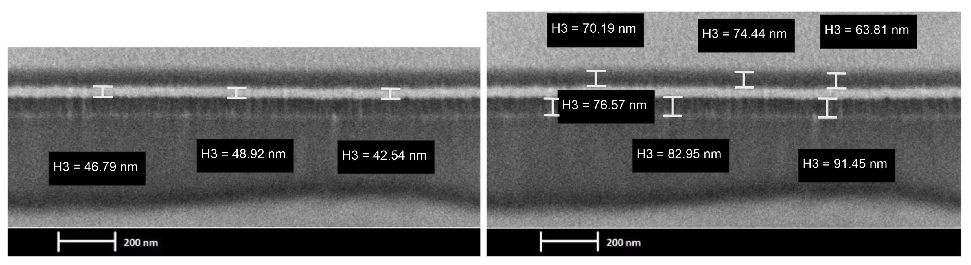
| Ag/AlN/Ag | 20/40/20 | 86 ± 1 | - | Meets expectations | |
| Ag/AlN/Ag | 20/40/20 | 89 ± 2 | - | Meets expectations | |
| Ag/AlN/Ag | 40/40/40 | 128 ± 3 | - | Meets expectations | |
| Ag/AlN/Ag | 60/40/60 | 172 ± 2 | 199 | Meets expectations |
Disclaimer/Publisher’s Note: The statements, opinions and data contained in all publications are solely those of the individual author(s) and contributor(s) and not of MDPI and/or the editor(s). MDPI and/or the editor(s) disclaim responsibility for any injury to people or property resulting from any ideas, methods, instructions or products referred to in the content. |
© 2024 by the authors. Licensee MDPI, Basel, Switzerland. This article is an open access article distributed under the terms and conditions of the Creative Commons Attribution (CC BY) license (https://creativecommons.org/licenses/by/4.0/).
Share and Cite
Behl, C.; Behlert, R.; Seiler, J.; Helke, C.; Shaporin, A.; Hiller, K. Characterization of Thin AlN/Ag/AlN-Reflector Stacks on Glass Substrates for MEMS Applications. Micro 2024, 4, 142-156. https://doi.org/10.3390/micro4010010
Behl C, Behlert R, Seiler J, Helke C, Shaporin A, Hiller K. Characterization of Thin AlN/Ag/AlN-Reflector Stacks on Glass Substrates for MEMS Applications. Micro. 2024; 4(1):142-156. https://doi.org/10.3390/micro4010010
Chicago/Turabian StyleBehl, Christian, Regine Behlert, Jan Seiler, Christian Helke, Alexey Shaporin, and Karla Hiller. 2024. "Characterization of Thin AlN/Ag/AlN-Reflector Stacks on Glass Substrates for MEMS Applications" Micro 4, no. 1: 142-156. https://doi.org/10.3390/micro4010010