Article

Enhancing the Photovoltaic Performance of Cd(1−x)ZnxS Thin Films Using Seed Assistance and EDTA Treatment

by
Gayan W. C. Kumarage
1,*,
Ruwan P. Wijesundera
1,
Elisabetta Comini
2 and
Buddhika S. Dassanayake
3
1
Department of Physics and Electronics, Faculty of Science, University of Kelaniya, Kelaniya 11600, Sri Lanka
2
Sensor Laboratory, Department of Information Engineering, University of Brescia, 25123 Brescia, Italy
3
Department of Physics, Faculty of Science, University of Peradeniya, Peradeniya 20400, Sri Lanka
*
Author to whom correspondence should be addressed.
Micro 2023, 3(4), 867-878; https://doi.org/10.3390/micro3040059
Submission received: 9 October 2023 / Revised: 3 November 2023 / Accepted: 9 November 2023 / Published: 12 November 2023

Abstract

:
This research article provides a comprehensive investigation into the optoelectronic characteristics of three distinct types of cadmium sulfide (CdS) thin films, namely: (a) conventionally prepared CdS thin films using chemical bath deposition (CBD-CdS), (b) CdS thin films produced via chemical bath deposition with the inclusion of zinc (CBD-Cd(1−x)ZnxS, x = 0.3), and (c) CdS thin films synthesized using a seed-assisted approach, treated with ethylenediaminetetraacetic acid (EDTA), and incorporating zinc (ED/CBD + EDTA-Cd(1−x)ZnxS). The investigation reveals that the crystallite size of these thin films decreases upon the addition of EDTA to the reaction solution, leading to an increase in the inter-planar spacing and dislocation density. Furthermore, a blue shift in the transmittance edge of the ED/CBD + EDTA-Cd(1−x)ZnxS samples compared to CBD-CdS implies modifications in the band gaps of the deposited films. The incorporation of Zn2+ into the reaction solution results in an increased band gap value of up to 2.42 eV. This suggests that Cd(1−x)ZnxS thin films permit more efficient photon transmission compared to conventional CdS. Among the three types of films studied, ED/CBD + EDTA-Cd(1−x)ZnxS exhibits the highest optical band gap of 2.50 eV. This increase in the optical band gap is attributed to the smaller crystallite size and the splitting of the tail levels from the band structure. Additionally, the increment in the optical band gap leads to reduced light absorption at longer wavelengths, thereby enhancing the electrical properties. Notably, ED/CBD + EDTA-Cd(1−x)ZnxS thin films demonstrate improved photovoltaic performance in a photoelectrochemical (PEC) cell, characterized by enhanced open-circuit voltage (363 mV, VOC), short-circuit current (35.35 μA, ISC), and flat-band voltage (−692 mV, Vfb). These improvements are attributed to the better adhesion of CdS to the fluorine-doped tin oxide (FTO) substrate and improved inter-particle connectivity.

1. Introduction

Semiconductor materials find widespread practical applications across various fields due to their unique electrical and optical properties [1,2,3,4]. Among the diverse range of semiconductor materials, II-VI group semiconductors such as cadmium sulfide (CdS), cadmium telluride (CdTe), zinc selenide (ZnSe), and zinc sulfide (ZnS) have emerged as leading candidates for applications such as solar cells, light-emitting diodes, lasers, thin film transistors, piezoelectric devices, infrared detectors, and light detectors. This preference is attributed to their direct and wide band gaps, as well as high carrier effective mass [5,6,7].
In thin-film solar cell technologies, CdTe-based solar cells are the most commercially successful option due to their cost-effectiveness, efficiency, stability, and large-scale production. Within CdTe-based solar cells, the window layer plays a pivotal role in determining the solar cell’s overall efficiency. N-type CdS has proven to be an excellent choice for serving as the transparent window layer in CdTe-based heterojunction structures [8,9,10]. CdS itself possesses a direct band gap of 2.38 eV (in the cubic, metastable phase), 2.58 eV (in the wurtzite, stable phase) [11] and CdS is known for its stability and durability, which is essential for the long-term performance and reliability of CdTe solar cells. Conversely, CdS can passivate the grain boundaries within CdTe, resulting in a reduction in recombination and an improvement in the overall efficiency of the solar cell.
Generally, the thickness of the CdS layer should be less than 100 nm to transmit the bulk of the solar irradiation to the absorber material (CdTe) to achieve a high photocurrent density. However, narrowing down the thickness may result in the occurrence of pinholes, which can adversely affect the open circuit voltage and, hence, the conversion efficiency of the solar cells [12]. Therefore, selecting the most suitable deposition method that minimizes pinhole occurrence and yields a uniform film is crucial. CdS thin films can be deposited using many growth procedures such as electrodeposition (ED), chemical bath deposition (CBD), molecular beam epitaxy (MBE), spray pyrolysis, chemical vapor deposition (CVD), screen printing, and successive ionic layer adsorption and reaction (SILAR) deposition etc. [13,14,15]. However, reports on the use of combined growth techniques for the growth of CdS thin films and the study of their properties are rarely found in the literature [16,17].
Recent studies have indicated that the inclusion of ethylenediaminetetraacetic acid (EDTA) in the chemical bath deposition (CBD) process for CdS results in the formation of nanosized crystals. This, in turn, enhances the photoactivity of the CdS thin films by increasing the surface roughness and effective surface area [15]. Electrodeposited CdS (ED-CdS) thin films exhibit superior uniformity and adhere well to surfaces, particularly fluorine-doped tin oxide glass substrates [18,19]. Therefore, there is significant interest in exploring the combined deposition approach involving both ED-CdS and CBD-CdS with the addition of EDTA [16].
Another promising method for improving the optoelectrical properties of CdS thin films involves the incorporation of metal compounds such as In, Zn, or Ga [20]. Among these options, the incorporation of Zn into CdS thin films is particularly advantageous due to the almost similar ionic radii of Zn2+ (0.074 nm) and Cd2+ (0.095 nm) [21,22]. Additionally, the introduction of Zn2+ along with Cd2+ alters the optical transmittance of heterojunction solar cells by forming Cd(1−x)ZnxS ternary semiconductors. This alteration allows more photons to pass into the absorber layer when these films are employed in solar cells, thereby enhancing their efficiency [13,23].
It is postulated that the electrochemical process encompassing the electrodeposition of CdS, facilitated by seed crystals, and subsequent Zn doping within an EDTA-infused chemical bath (ED/CBD + EDTA-Cd(1−x)ZnxS), yields improved optoelectronic properties when compared to traditional methods involving CBD-CdS and Cd(1−x)ZnxS deposition. Remarkably, no prior scholarly work has been conducted utilizing these particular methodologies, as per the current state of knowledge held by the authors.
This investigation holds significance in the context of advancing the synthesis of materials at the nano- or micro-scale. The employment of seed-assisted growth in conjunction with EDTA treatment implies an elevated degree of precision and control at the nano-scale in the fabrication of Cd(1−x)ZnxS thin films. Additionally, this study contributes to the broader field of material engineering, where the exploration of the impacts of seed-assisted growth and EDTA treatment on Cd(1−x)ZnxS thin films entails deliberate modifications at the micro- and nano-scale to engineer materials with the desired properties, a pivotal facet of material engineering within the micro- and nano-scale domain.
Accordingly, we provide a comprehensive exploration of the improvements in the morphological, optical, and electronic properties of grown CdS thin films achieved by using an ED-CdS layer as a seed, along with incorporating EDTA and Zn. To investigate the impact of EDTA, the ED-CdS seed layer, and Zn incorporation on these properties, we conducted Grazing Incident X-ray Diffraction (GIXRD), UV-visible, C-V, and photoelectrochemical (PEC) cell measurements. Consequently, this study appears to introduce an innovative methodology (EDTA treatment) and a potentially unique combination of techniques. By extending the existing knowledge in this field, it provides insights that can potentially steer forthcoming research endeavors in the field of micro- and nano-scale.

2. Materials and Methods

All the chemicals used in this reporting study were analytical reagent grade. Deionized water was used for the preparation of all aqueous solutions. The chemicals and their respective specifications are shown in Table 1. The FTO glass substrates (TEC 10, Sigma-Aldrich, St. Louis, MO, USA) were subjected to pre-deposition cleaning, which involved sequential steps. Initially, the substrates were cleansed using diluted HCl (ACS reagent, 37%, Sigma-Aldrich, USA) followed by rinsing with de-ionized water and subsequent ultrasound sonication. Later, the cleaning procedure continued using a series of organic solvents, namely acetone (ACS reagent, ≥99.5%, Sigma-Aldrich, USA), methanol (ACS reagent, ≥99.5%, Sigma-Aldrich, USA), and isopropanol (ACS reagent, ≥99.5%, Sigma-Aldrich, USA). Each solvent was utilized for cleaning the substrates at a temperature of 70 °C via immersion, and the substrates were properly dried using nitrogen gas afterward. [3,24,25].

2.1. Deposition of Chemical-Bath-Deposited CdS (CBD-CdS) Thin Films

The CBD-CdS thin films were deposited onto FTO glass substrates using 3CdSO4.8H2O (1 mM), CS(NH2)2 (2 mM), and a NH4OH solution (1.1 mL) as reagents at a bath temperature of 80 °C, stirring the reaction solution at a rate of 200 rpm. The conducting glass substrates were positioned inside a beaker at an angle of 45° in the solution using a custom-designed Teflon sample holder. A detailed description of the methodology can be found in our previous publication [26].

2.2. Deposition of Chemical-Bath-Deposited Cd1−xZnxS (CBD-Cd(1−x)ZnxS; x = 0.3) Thin Films

Cd1xZnxS (CBD-Cd(1x)ZnxS; x = 0.3) films were grown on FTO glass substrates using the reagents; 3CdSO4.8H2O (0.47 mM), ZnSO4.7H2O (0.53 mM), CS(NH2)2 (2 mM), and NH4OH solution (1.1 mL). The conducting glass substrates were positioned inside a beaker at an angle of 45° in the solution using a custom-designed Teflon sample holder. The bath temperature was maintained at 80 °C while stirring the reaction solution at a rate of 200 rpm. A detailed description of the methodology can be found in our previous publication [26].

2.3. Deposition of Seed-Assisted Cd(1−x)ZnxS with EDTA Treatment (x = 0.3 in the Reaction Solution)

First, a seed layer of ED-CdS was deposited onto the FTO glasses using CdCl2. 2½ H2O (0.05 M) and Na2S2O3 (0.05 M) in a three-electrode system under a pH of 1–2 at a bath temperature of 60 °C. The seeds of ED-CdS were deposited for a duration of 3 min. A detailed description of the deposition of a ED-CdS seed can be found in our previous publication [16].
In order to deposit the Zn-incorporated EDTA-assisted CdS on top of the ED-CdS seed layer, the same chemical bath described in Section 2.2 was used with EDTA (0.2 mM) in the reaction vessel. All the other deposition parameters were kept as in Section 2.1 and Section 2.2. All the grown films under the three deposition methods were air-annealed at 200 °C for one hour in a tube furnace (Büchi TO-51).

3. Characterization

The grown CdS films underwent morphological characterization utilizing the Zeiss EVO|LS15 system. To assess the structural properties of the deposited films, GIXRD analysis was conducted employing a Panalytical diffractometer (Empyrean). The instrumental parameters employed for this characterization included CuKα radiation with a wavelength of 1.54184 Å and a 2° incident angle, operating at 40 kV and 40 mA. Optical characterizations were performed using a UV-1800 Shimadzu UV-vis spectrophotometer. To determine the thickness of the deposited CdS films, a Profilometer (XP-1) and SEM cross-sections were employed.
All PEC cell analyses were carried out on a Pt/0.1 mol.dm−3 Na2S2O3/CdS/FTO setup, utilizing PEC Cell L01. The illuminated area of the CdS/electrolyte interface measured 0.25 cm2. AM 1.5 simulated solar light irradiation was generated using a 150 W short-arc xenon lamp and directed onto the CdS/electrolyte junction. The same PEC cell configuration was employed for the capacitance–voltage (C–V) measurements, which were conducted using a sinusoidal signal of 1000 Hz and a voltage of 20 mV corresponding to the Ag/AgCl electrode.

4. Results and Discussion

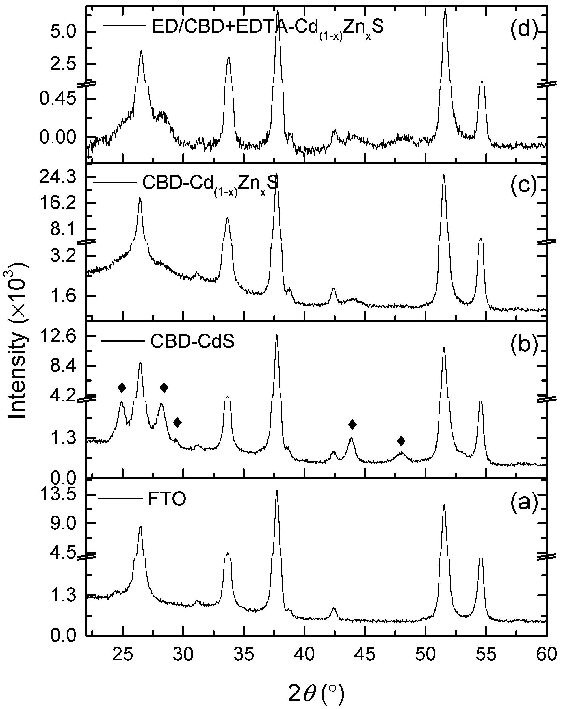
4.1. Structural Characterization

Figure 1 displays the GIXRD diffractograms obtained for three distinct thin film samples: CBD-CdS, CBD-Cd(1−x)ZnxS, and ED/CBD + EDTA-Cd(1−x)ZnxS. For comparison, the XRD pattern of the FTO substrates is also included in Figure 1a, in addition to the XRD patterns of the CBD-CdS, CBD-Cd(1−x)ZnxS, and ED/CBD + EDTA-Cd(1−x)ZnxS thin films. In Figure 1b–d, the reflections are observed at specific 2θ angles of 25.07°, 26.46°, 28.32°, 44.10°, and 48.34°. These peaks correspond to (100), (002), (101), (110), and (103) planes of hexagonal CdS (JCPDS 98-009-5006 and 06-0314). Also, the 2θ peaks corresponding to the planes of (100) and (101) were found to broaden in both CBD-Cd(1−x)ZnxS and ED/CBD + EDTA-Cd(1−x)ZnxS compared to that of CBD-CdS. The variation in the diffraction peaks may be due to the poor crystallinity or the formation of nano-sized crystals resulting from Zn2+ incorporation into the CdS matrix [13,16,26]. No peaks of any other phase or impurity are noticed in the Zn-incorporated samples (Figure 1c,d). Thus, it can be determined that the films grown with Zn were not a blend of CdS and ZnS, but Cd1−xZnxS. The intensity of the (100), (101), (110), and (103) reflections of Cd1−xZnxS were found to be significantly increased.
The crystallite size was estimated using the highest intensity planes (100), (002), (101), (110), and (103) using the relation [27];
β cos θ = K λ D + 4 ε sin θ
where λ is the wavelength of the CuKα radiation (λ = 1.54184 Å), θ is the Bragg angle, D is the average diameter of the grains, β is the FWHM of the diffraction peak, ε is the residual strain of the film, and K is the shape factor, which is approximately 0.94. The value of ε was obtained from the gradient of the βcosθ vs. sinθ plot. The obtained values of D, ε, and δ (dislocation density) for the films CBD-CdS, CBD-Cd(1−x)ZnxS, and ED/CBD + EDTA-Cd(1−x)ZnxS are tabulated in Table 2.
Table 2 shows that the addition of Zn to the reaction bath has significantly changed the crystal size of the grown films. The alternation of the average crystallite size with the deposition method is also clear from the broadness of the XRD peak widths. This also reveals the increment in the lattice imperfections due to the increment in the internal micro-strain from CBD-CdS to ED/CBD + EDTA-Cd(1−x)ZnxS.
The crystallite size was found to decrease with the addition of EDTA to the reaction solution. Such a decrease in crystallite size may increase the inter-planar spacing as well as the dislocation density [28]. Hence, this variation found in the diffraction peak is an indication of different optical, electrical, as well as morphological changes in the grown films.

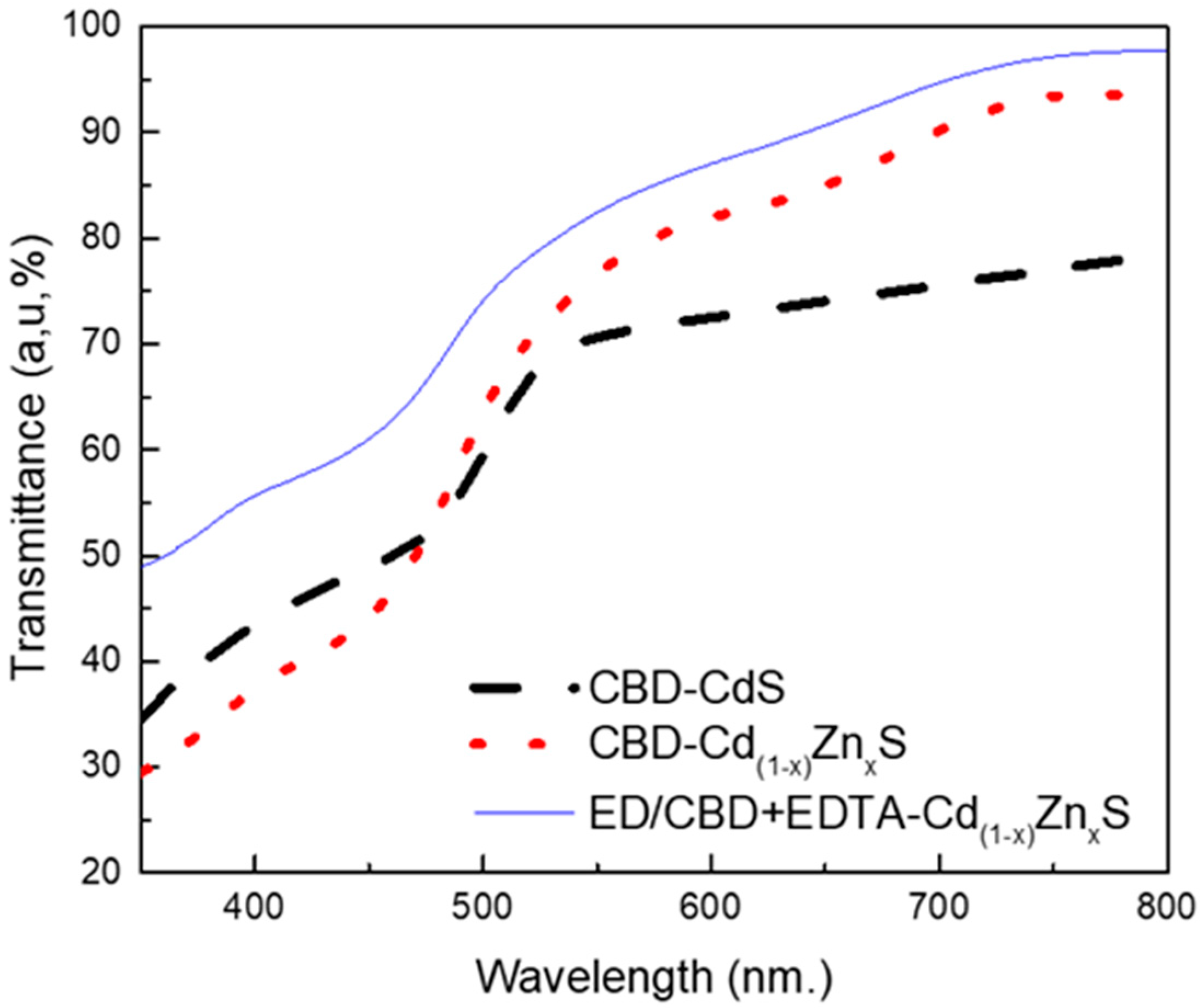
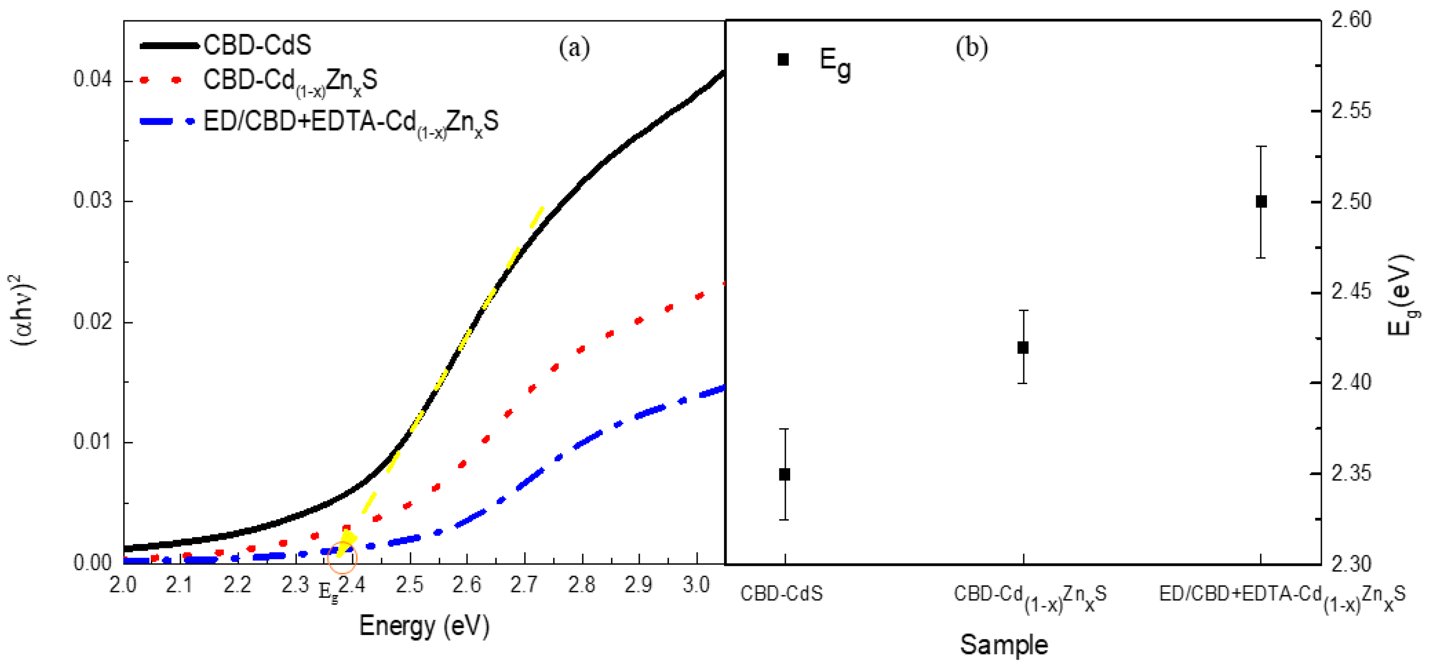
4.2. Optical Characterization

Figure 2 presents the transmittance spectra of CdS films grown using different deposition methods. The average transmittance values of CBD-Cd(1−x)ZnxS and ED/CBD + EDTA-Cd(1−x)ZnxS are higher compared to that of CBD-CdS in the wavelength region of 550–800 nm. Among the grown films, ED/CBD + EDTA-Cd(1−x)ZnxS produces the highest transmittance (>85%) in the wavelength range of 550–800 nm, as shown in Figure 2. Furthermore, the transmittance edge of the samples CBD-Cd(1−x)ZnxS to ED/CBD + EDTA-Cd(1-x)ZnxS was found to shift toward the lower wavelength region (blue shift) compared to CBD-CdS, indicating that the band gaps of the deposited films have been subjected to change. The blue shift of the band edge is desirable as it suggests an increase in the band gap of the thin film.
The optical band gap (Eg) values of the CdS films were obtained by extrapolating the linear (αhυ)2 vs. plots (Figure 3a) derived from the Stern relation [29,30,31,32,33,34]:
α = A h ν E g n 2 h ν
where h is Planck’s constant, A is a constant, α is the optical absorption coefficient, and n is equal to 1 for CdS. Although the band gap of the grown CBD-CdS is 2.35 eV, it can be seen from Table 3 and Figure 3b that adding Zn2+ to the reaction solution helps increase the band gap value up to 2.42 eV. This suggests that Cd(1−x)ZnxS thin films permit more photons to transmit through the film compared to conventional CdS [35]. Out of the three different types of films grown, the highest optical band gap of 2.50 eV (Figure 3) was obtained in ED/CBD + EDTA-Cd(1−x)ZnxS. The increase in optical band gap can be related to the smaller crystallite size, as shown in Table 2, as well as the splitting of the tail levels from the band [36]. The increment in the optical band gap reduces the absorption of light in the regimes of a longer wavelength, which in turn enhances the electrical properties [28,30].

4.3. Electrical Characterization

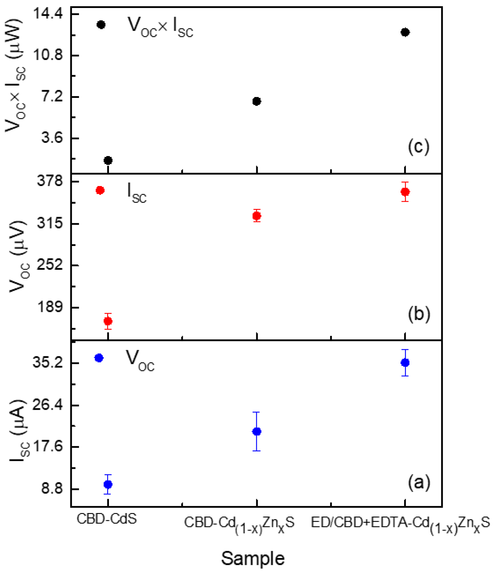
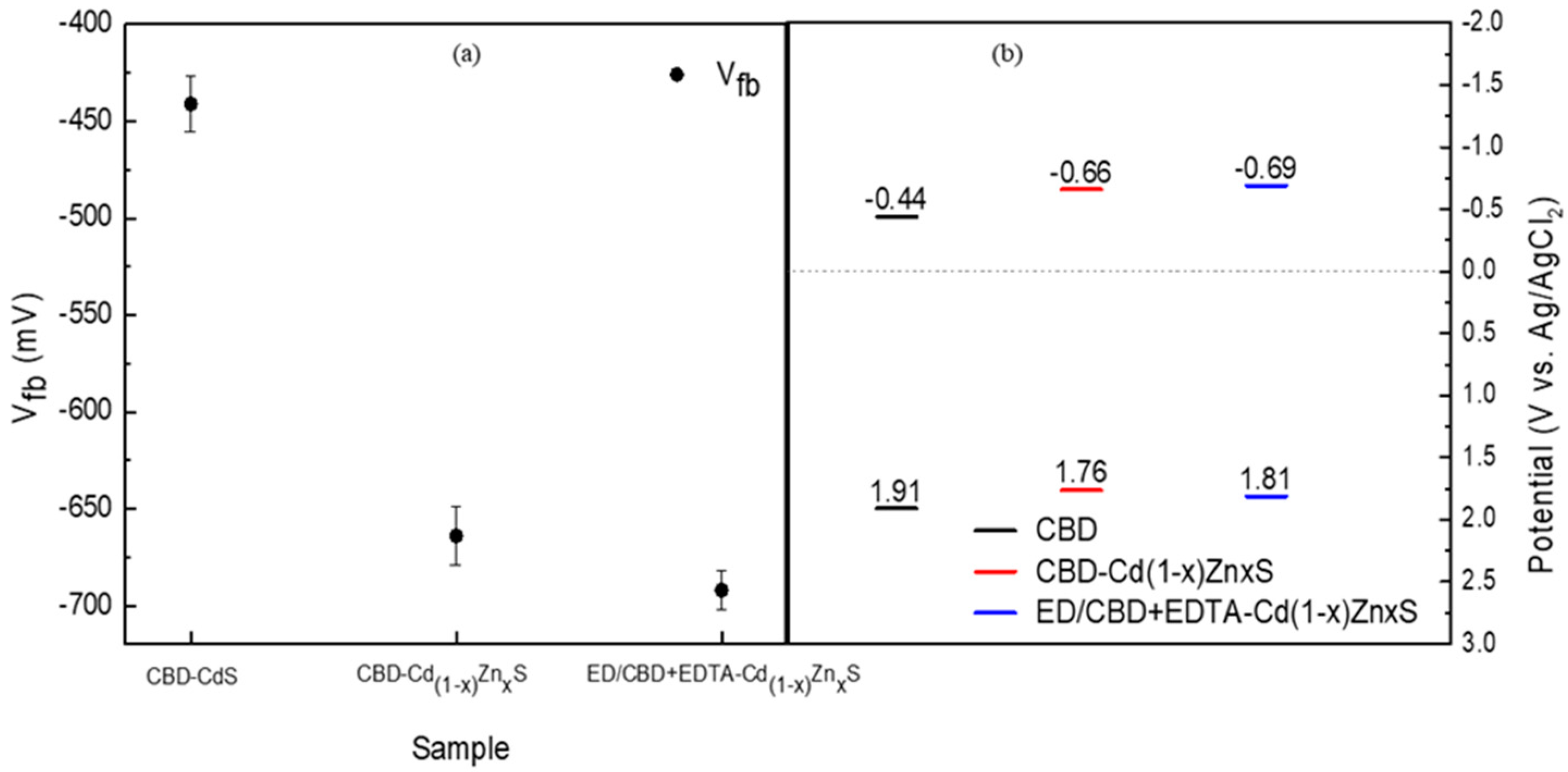
4.3.1. PEC Cell Characterization

Figure 4 illustrates a plot depicting the open-circuit voltage (VOC), short-circuit current (ISC), and the product of VOC and ISC for the three distinct sets of grown films. It was observed that both the ISC and VOC values increased notably with the introduction of Zn and EDTA treatment. Specifically, the film ED/CBD + EDTA-Cd(1−x)ZnxS exhibited the highest ISC values (as depicted in Figure 4a and detailed in Table 3). This enhancement in the ISC values in the ED/CBD + EDTA-Cd(1−x)ZnxS films can be attributed to improved inter-particle connections and enhanced adherence of the ED-CdS seed to the FTO substrates compared to conventional CBD-CdS and CBD-Cd(1−x)ZnxS films, as previously discussed [15]. Furthermore, the superior photoactivity observed in the ED/CBD + EDTA-Cd(1−x)ZnxS film can be attributed to the well-interconnected network structure, which facilitates the efficient flow of charge carriers.

4.3.2. C-V Characterization

The flat-band potential (Vfb) and carrier concentration (ND) of the deposited CdS films were obtained (Table 3 and Figure 5a) from the X-axis intercept and the gradient of the linear fit of the Mott–Schottky equation used [2,3,37,38].
1 C 2 = 2 A ε ε 0 N D ( V V f b k T e )
In the given equations, “e” represents the charge of an electron, “ε” (with a value of 8.5) denotes the dielectric constant, “ε0” stands for the permittivity in a vacuum, “A” is the area of the depletion region, “k” is the Boltzmann constant, and “T” is the absolute temperature [39]. Although not shown, the Mott–Schottky plots confirmed the n-type behavior exhibited by all the Cd(1−x)ZnxS thin films fabricated in this study.
The flat-band potential and carrier concentration were observed to be at their lowest levels in the case of the conventional CBD-CdS films. Conversely, the improved net donor density (ND) in the ED/CBD + EDTA-Cd(1−x)ZnxS film, as evident in Table 3, can be linked to the enhancement of the ISC value. Notably, ED/CBD + EDTA-Cd(1−x)ZnxS exhibited the highest flat-band voltage (Vfb) among all the grown CdS films. The higher VOC observed in films incorporating zinc (Zn) can be attributed to the increased energy gap (Eg) and Vfb, as shown in Table 3.
The rise in Vfb in the films incorporating Zn may be attributed to the formation of donor levels that effectively shift the relative energy band positions, leading to increased band bending and subsequently an elevated VOC, as depicted in Figure 4b. The presence of distinct Vfb values supports the idea of varying relative conduction band levels within the grown CdS thin films, warranting further investigation into their energy band structures.
In typical unbiased n-type semiconductors, it is reasonable to assume a flat potential near the position of the bottom of the conduction band (ECB) [40]. Utilizing ECB as a reference point, it becomes possible to determine the valence band-edge potential (EVB) of the deposited thin films [41,42].
EVB = ECB + Eg
The investigated energy band structure with respect to the Ag/AgCl is shown in Figure 5b. The figure shows the presence of different energy band levels in the grown films. The existence of different energy band levels in a material suggests the possibility of overcoming energy spikes in the depletion region in a p-n junction [15].

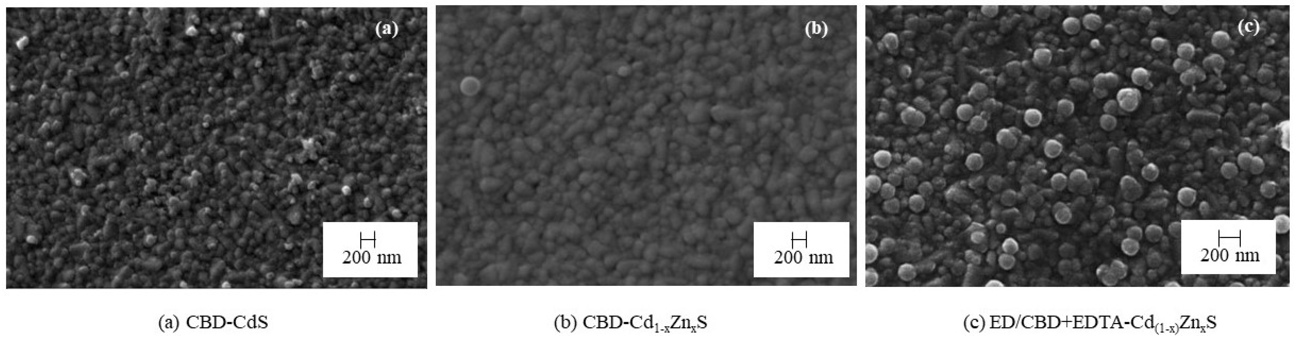
4.4. Morphological Characterization

Figure 6a–c shows the SEM images of CBD-CdS, CBD-Cd(1−x)ZnxS, and ED/CBD + EDTA-Cd(1−x)ZnxS, respectively. The CBD-CdS films show uniform and smooth clusters without creaks or apparent pinholes and cover the glass substrate appreciably well, as seen in Figure 6a. With the addition of Zn2+ into the reaction solution (x = 0.3), small uniform grains with well-defined grain boundaries were found to form (Figure 6b), potentially increasing the roughness. Hence, the effective surface area of the Zn-incorporated films enhanced the ISC values (Table 3). Figure 6c shows an SEM image of the ED/CBD + EDTA-Cd(1−x)ZnxS film, which consists of some apparent spherical features and is clearly different from the other two types of films grown. The SEM images of ED/CBD + EDTA-Cd(1−x)ZnxS show more uniform coagulates associated with CBD and CBD-Cd(1−x)ZnxS, suggesting that the ED/CBD layer has greatly influenced the morphology of the CBD-CdS layer. Moreover, it is also found in the literature that the electrochemical deposition gives CdS in the hexagonal phase improved uniformity, packing, and better attachment to the FTO [8,43]. This could also be a reason for the improved ISC values in the ED/CBD + EDTA-Cd1−xZnxS system.

5. Conclusions

This study comprehensively evaluates thin films, emphasizing their structural, optical, and electrical attributes influenced by varying deposition techniques. The GIXRD patterns of CBD-CdS, CBD-Cd(1−x)ZnxS, and ED/CBD + EDTA-Cd(1−x)ZnxS films reveal distinctive alterations in the films’ crystallinity and grain morphology. These X-ray diffraction patterns unveil essential insights into the structural evolution brought about by the deposition processes.
The incorporation of zinc (Zn) in conjunction with EDTA treatment in seed-assisted CdS thin films induces a blue shift in the absorption edge, setting them apart from their pure CdS counterparts. This shift significantly modifies the optical band gap, elevating it from 2.35 to 2.50 eV. These values exhibit a consistent increment as we transition from CBD-CdS to CBD-Cd(1−x)ZnxS, culminating in the ED/CBD + EDTA-Cd(1−x)ZnxS film. This rise in the band gap is primarily ascribed to the reduction in crystallite size and consequential shifts in energy levels. These alterations, in turn, influence light absorption and electrical characteristics, making them pivotal factors in the films’ performance. Accordingly, when comparing CBD-Cd(1−x)ZnxS to CBD-CdS, a noteworthy enhancement in key photovoltaic parameters was evident. Specifically, open-circuit voltage (VOC), short-circuit current density (Jsc), and flat-band voltage (Vfb) experienced substantial increments of 93%, 114%, and 50%, respectively, in the case of CBD-Cd(1−x)ZnxS in contrast to CBD-CdS. A similar trend was observed with ED/CBD + EDTA-Cd(1−x)ZnxS, showcasing remarkable improvements with increases of 114%, 263%, and 57% for VOC, Jsc, and Vfb, respectively, when compared to CBD-CdS. Therefore, it can be stated that the deposition method employed influences the relative energy band positions. ED/CBD + EDTA-Cd(1−x)ZnxS emerges as the leader in terms of Vfb, in agreement with the significant shift in energy band positions and well-connected network structure. These shifts bear far-reaching implications for the energy band structures of the films.
The exceptional optoelectrical characteristics observed in ED/CBD + EDTA-Cd(1−x)ZnxS can be attributed to several contributing factors, as initially postulated. These factors include superior adhesion of CdS to the FTO (fluorine-doped tin oxide) substrate, enhanced carrier concentrations, unique spherical features, and improved inter-particle connectivity.
These findings contribute to the current body of knowledge and can potentially guide future research in the micro-and nano-scale domain. The impact of this research extends beyond the laboratory, holding promise for advanced semiconductor technology and photovoltaics applications. In summary, the synergistic combination of Zn incorporation and EDTA treatment in seed-assisted CdS thin films presents a compelling avenue for optimizing their optoelectronic properties, with far-reaching implications for emerging micro- and nano-scale technologies.

Author Contributions

Conceptualization, G.W.C.K. and B.S.D.; methodology, G.W.C.K.; validation, B.S.D., R.P.W. and E.C.; formal analysis, G.W.C.K.; investigation, G.W.C.K.; resources, B.S.D., R.P.W. and E.C.; data curation, G.W.C.K.; writing—original draft preparation, G.W.C.K.; writing—review and editing, B.S.D., R.P.W. and E.C.; visualization, G.W.C.K.; supervision, B.S.D., R.P.W. and E.C.; project administration, B.S.D.; funding acquisition, B.S.D. All authors have read and agreed to the published version of the manuscript.

Funding

This research was funded by the Edu-Training National Solar Project of the State Ministry of Skills Development, Vocational Education, Research & Innovation, Sri Lanka.

Data Availability Statement

The data presented in this study are available on request from the corresponding author.

Acknowledgments

A portion of the research was conducted at the Sensor Lab within the Department of Information Engineering at the University of Brescia, located in Brescia, Italy.

Conflicts of Interest

The authors declare no conflict of interest.

References

  1. Dharmadasa, I.M.; Alam, A.E.; Ojo, A.A.; Echendu, O.K. Scientific Complications and Controversies Noted in the Field of CdS/CdTe Thin Film Solar Cells and the Way Forward for Further Development. J. Mater. Sci. Mater. Electron. 2019, 30, 20330–20344. [Google Scholar] [CrossRef]
  2. Karthikeyan, C.; Arunachalam, P.; Ramachandran, K.; Al-Mayouf, A.M.; Karuppuchamy, S. Recent Advances in Semiconductor Metal Oxides with Enhanced Methods for Solar Photocatalytic Applications. J. Alloys Compd. 2020, 828, 154281. [Google Scholar] [CrossRef]
  3. Kang, S.; Lee, D.; Kim, J.; Capasso, A.; Kang, H.S.; Park, J.-W.; Lee, C.-H.; Lee, G.-H. 2D Semiconducting Materials for Electronic and Optoelectronic Applications: Potential and Challenge. 2D Mater. 2020, 7, 022003. [Google Scholar] [CrossRef]
  4. Yan, L.L.; Wang, X.B.; Cai, X.J.; Li, X.J. Effect of Boron-Doping on the Luminescent and Electrical Properties of a CdS/Si Heterostructure Based on Si Nanoporous Pillar Array. J. Alloys Compd. 2015, 632, 450–455. [Google Scholar] [CrossRef]
  5. Dhaygude, H.D.; Shinde, S.K.; Takale, M.V.; Dubal, D.P.; Lohar, G.M.; Fulari, V.J. Electrodeposited Nanosphere like CdxZn1−xS Electrodes for Photoelectrochemical Cell. J. Mater. Sci. Mater. Electron. 2016, 27, 5145–5152. [Google Scholar] [CrossRef]
  6. Dobson, K.D.; Visoly-Fisher, I.; Hodes, G.; Cahen, D. Stability of CdTe/Cds Thin-Film Solar Cells. Sol. Energy Mater. Sol. Cells 2000, 62, 295–325. [Google Scholar] [CrossRef]
  7. Zhou, L.; Hu, X.; Wu, S. Effects of Deposition Temperature on the Performance of CDS Films with Chemical Bath Deposition. Surf. Coat. Technol. 2013, 228, S171–S174. [Google Scholar] [CrossRef]
  8. Lilhare, D.; Khare, A. Temperature Dependent Characterizations of Chemically Deposited (CDX-ZN1-X)s Nanocrystalline Films for Solar Cell Applications. Opt. Mater. 2020, 108, 110385. [Google Scholar] [CrossRef]
  9. Ashok, A.; Regmi, G.; Romero-Núñez, A.; Solis-López, M.; Velumani, S.; Castaneda, H. Comparative Studies of Cds Thin Films by Chemical Bath Deposition Techniques as a Buffer Layer for Solar Cell Applications. J. Mater. Sci. Mater. Electron. 2020, 31, 7499–7518. [Google Scholar] [CrossRef]
  10. Kumarage, W.C. Are thin film solar cells the solution for energy crisis? Sciscitator 2015, 2, 44–47. [Google Scholar]
  11. Nakada, T.; Ohbo, H.; Fukuda, M.; Kunioka, A. Improved Compositional Flexibility of Cu(In,Ga)Se2-Based Thin Film Solar Cells by Sodium Control Technique. Sol. Energy Mater. Sol. Cells 1997, 49, 261–267. [Google Scholar] [CrossRef]
  12. Zhou, J.; Wu, X.; Teeter, G.; To, B.; Yan, Y.; Dhere, R.G.; Gessert, T.A. CBD-Cd1−xZnxS Thin Films and Their Application in CdTe Solar Cells. Phys. Status Solidi 2004, 241, 775–778. [Google Scholar] [CrossRef]
  13. Niles, D.W.; Höchst, H. Band Offsets and Interfacial Properties of Cubic CdS Grown by Molecular-Beam Epitaxy on CdTe(110). Phys. Rev. B 1990, 41, 12710–12719. [Google Scholar] [CrossRef] [PubMed]
  14. Kuhaimi, S.A. Influence of Preparation Technique on the Structural, Optical and Electrical Properties of Polycrystalline CDS Films. Vacuum 1998, 51, 349–355. [Google Scholar] [CrossRef]
  15. Yadav, A.A.; Masumdar, E.U. Photoelectrochemical Investigations of Cadmium Sulphide (CdS) Thin Film Electrodes Prepared by Spray Pyrolysis. J. Alloys Compd. 2011, 509, 5394–5399. [Google Scholar] [CrossRef]
  16. Kumarage, W.G.C.; Wijesundera, R.P.; Seneviratne, V.A.; Jayalath, C.P.; Varga, T.; Nandasiri, M.I.; Dassanayake, B.S. Growth and Characterization of EDTA Assisted CBD-CdS. Mater. Chem. Phys. 2017, 200, 1–8. [Google Scholar] [CrossRef]
  17. Zyoud, A.; Saadeddin, I.; Khurduj, S.; Mari’e, M.; Hawash, Z.M.; Faroun, M.I.; Campet, G.; Park, D.; Hilal, H.S. Combined Electrochemical/Chemical Bath Depositions to Prepare CdS Film Electrodes with Enhanced PEC Characteristics. J. Electroanal. Chem. 2013, 707, 117–121. [Google Scholar] [CrossRef]
  18. Akif Shikhan Aliyev, M.; El-rouby, M. Electrochemical Studies on the Cathodic Electrodeposition of N-Type Semiconductor CdS Thin Film from Thiosulfate Acidic Aqueous Solution. Int. J. Thin Film. Sci. Technol. 2013, 2, 195–205. [Google Scholar] [CrossRef] [PubMed]
  19. Kumarage, W.G.C.; Wijesundera, R.P.; Kaur, N.; Zappa, D.; Seneviratne, V.A.; Jayalath, C.P.; Dassanayake, B.S. A Comparative Assessment: Chemical Bath Deposited and Electrodeposited CdS Films. Int. J. Electroact. Mater. 2019, 7, 1–6. [Google Scholar]
  20. Yang, X.; Wang, Z.; Lv, X.; Wang, Y.; Jia, H. Enhanced Photocatalytic Activity of Zn-Doped Dendritic-like CdS Structures Synthesized by Hydrothermal Synthesis. J. Photochem. Photobiol. A Chem. 2016, 329, 175–181. [Google Scholar] [CrossRef]
  21. Chai, Y.-Y.; Qu, D.-P.; Ma, D.-K.; Chen, W.; Huang, S. Carbon Quantum Dots/Zn2+ Ions Doped-Cds Nanowires with Enhanced Photocatalytic Activity for Reduction of 4-Nitroaniline to P-Phenylenediamine. Appl. Surf. Sci. 2018, 450, 1–8. [Google Scholar] [CrossRef]
  22. Yang, F.; Yan, N.-N.; Huang, S.; Sun, Q.; Zhang, L.-Z.; Yu, Y. Zn-Doped Cds Nanoarchitectures Prepared by Hydrothermal Synthesis: Mechanism for Enhanced Photocatalytic Activity and Stability under Visible Light. J. Phys. Chem. C 2012, 116, 9078–9084. [Google Scholar] [CrossRef]
  23. Azizi, S.; Rezagholipour Dizaji, H.; Ehsani, M.H. Structural and Optical Properties of Cd1-xZnxS (x = 0, 0.4, 0.8 and 1) Thin Films Prepared Using the Precursor Obtained from Microwave Irradiation Processes. Optik 2016, 127, 7104–7114. [Google Scholar] [CrossRef]
  24. Kumarage, W.G.C.; Wijesundera, R.P.; Seneviratne, V.A.; Jayalath, C.P.; Kaur, N.; Comini, E.; Dassanayake, B.S. MgCl2 Activation of CdS Films: An Alternative for CdCl2. J. Photochem. Photobiol. A Chem. 2018, 367, 171–177. [Google Scholar] [CrossRef]
  25. Adikaram, K.K.; Kumarage, W.G.; Varga, T.; Dassanayake, B.S. Improvement of the Photo-Activity of CdS Thin Films Using TX-100. J. Electron. Mater. 2019, 48, 4424–4431. [Google Scholar] [CrossRef]
  26. Kumarage, W.G.; Wijesundera, R.P.; Seneviratne, V.A.; Jayalath, C.P.; Varga, T.; Dassanayake, B.S. Optical, Structural and Photo Electrochemical Properties of Cd1−xZnxS Films Grown by Chemical Bath Deposition. Appl. Phys. A 2018, 124, 494. [Google Scholar] [CrossRef]
  27. Monshi, A.; Foroughi, M.R.; Monshi, M.R. Modified Scherrer Equation to Estimate More Accurately Nano-Crystallite Size Using XRD. World J. Nano Sci. Eng. 2012, 2, 154–160. [Google Scholar] [CrossRef]
  28. Mariappan, R.; Ragavendar, M.; Ponnuswamy, V. Growth and Characterization of Chemical Bath Deposited Cd1−xZnxS Thin Films. J. Alloys Compd. 2011, 509, 7337–7343. [Google Scholar] [CrossRef]
  29. Moualkia, H.; Hariech, S.; Aida, M.S. Structural and Optical Properties of CdS Thin Films Grown by Chemical Bath Deposition. Thin Solid Film. 2009, 518, 1259–1262. [Google Scholar] [CrossRef]
  30. Oliva-Avilés, A.; Patiño, R.; Oliva, A. CdS films deposited by chemical bath under rotation. Appl. Surf. Sci. 2010, 256, 6090–6095. [Google Scholar] [CrossRef]
  31. Molina, J.; Horta, S.D.; Espejo-Bayona, L.; Castillo, S.J.; Avila, D.A. Comparative Study of the Optical Response in Thin Films of Cds. J. Phys. Conf. Ser. 2021, 1723, 012028. [Google Scholar] [CrossRef]
  32. Mukherjee, A.; Ghosh, P.; Aboud, A.A.; Mitra, P. Influence of Copper Incorporation in Cds: Structural and Morphological Studies. Mater. Chem. Phys. 2016, 184, 101–109. [Google Scholar] [CrossRef]
  33. Yadav, S.K.; Vishwakarma, A.K.; Yadava, L. Structural and Optical Properties of Cadmium Sulfide (Cds) Nano-powder. Macromol. Symp. 2023, 407, 2100441. [Google Scholar] [CrossRef]
  34. Kariper, A.; Güneri, E.; Göde, F.; Gümüş, C.; Özpozan, T. The Structural, Electrical and Optical Properties of CdS Thin Films as a Function of Ph. Mater. Chem. Phys. 2011, 129, 183–188. [Google Scholar] [CrossRef]
  35. Akyuz, I.; Kose, S.; Atay, F.; Bilgin, V. Some Physical Properties of Chemically Sprayed Zn1−xCdxS Semiconductor Films. Mater. Sci. Semicond. Process. 2007, 10, 103–111. [Google Scholar] [CrossRef]
  36. Jayaramaiah, J.R.; Lakshminarasappa, B.N.; Nagabhushana, B.M. Thermoluminescence Studies of Solution Combustion Synthesized Y2O3:Nd3+ Nanophosphor. Mater. Chem. Phys. 2011, 130, 175–178. [Google Scholar] [CrossRef]
  37. Gelderman, K.; Lee, L.; Donne, S.W. Flat-Band Potential of a Semiconductor: Using the Mott–Schottky Equation. J. Chem. Educ. 2007, 84, 685. [Google Scholar] [CrossRef]
  38. Kumarasinghe, R.K.; Kumarage, W.G.; Wijesundera, R.P.; Kaur, N.; Comini, E.; Dassanayake, B.S. A Comparative Study on CdS Film Formation under Variable and Steady Bath-Temperature Conditions. Semiconductors 2020, 54, 838–843. [Google Scholar] [CrossRef]
  39. Ozsan, M.E.; Johnson, D.R.; Sadeghi, M.; Sivapathasundaram, D.; Goodlet, G.; Furlong, M.J.; Peter, L.M.; Shingleton, A.A. Optical and Electrical Characterization of CdS Thin Films. J. Mater. Sci. Mater. Electron. 1996, 7, 119–125. [Google Scholar] [CrossRef]
  40. Finlayson, M.F.; Wheeler, B.L.; Kakuta, N.; Park, K.H.; Bard, A.J.; Campion, A.; Fox, M.A.; Webber, S.E.; White, J.M. Determination of Flat-Band Position of Cadmium Sulfide Crystals, Films, and Powders by Photocurrent and Impedance Techniques, Photoredox Reaction Mediated by Intragap States. J. Phys. Chem. 1985, 89, 5676–5681. [Google Scholar] [CrossRef]
  41. Guan, M.-L.; Ma, D.-K.; Hu, S.-W.; Chen, Y.-J.; Huang, S.-M. From Hollow Olive-Shaped BiVO4 to N−P Core−shell BiVO4@Bi2O3 Microspheres: Controlled Synthesis and Enhanced Visible-Light-Responsive Photocatalytic Properties. Inorg. Chem. 2010, 50, 800–805. [Google Scholar] [CrossRef] [PubMed]
  42. Bledowski, M.; Wang, L.; Ramakrishnan, A.; Khavryuchenko, O.V.; Khavryuchenko, V.D.; Ricci, P.C.; Strunk, J.; Cremer, T.; Kolbeck, C.; Beranek, R. Visible-Light Photocurrent Response of TiO2–Polyheptazine Hybrids: Evidence for Interfacial Charge-Transfer Absorption. Phys. Chem. Chem. Phys. 2011, 13, 21511. [Google Scholar] [CrossRef] [PubMed]
  43. Zyoud, A.; Saa’deddin, I.; Khudruj, S.; Hawash, Z.M.; Park, D.; Campet, G.; Hilal, H.S. CdS/FTO Thin Film Electrodes Deposited by Chemical Bath Deposition and by Electrochemical Deposition: A Comparative Assessment of Photo-Electrochemical Characteristics. Solid State Sci. 2013, 18, 83–90. [Google Scholar] [CrossRef]
Figure 1. GIXRD of the (a) bare FTO, (b) CBD-CdS on FTO, (c) CBD-Cd1−xZnxS on FTO, and (d) ED/CBD + EDTA-Cd(1−x)ZnxS on FTO where x = 0.3 in the reaction solution. The crystallographic planes of CdS are marked with ♦.
Micro 03 00059 g001
Figure 2. Transmittance spectra obtained for the fabricated CBD-CdS, CBD-Cd(1−x)ZnxS and ED/CBD+EDTA-Cd(1−x)ZnxS samples.
Micro 03 00059 g002
Figure 3. (a) Plot of (αhυ)2 vs. hυ (b) Optical band gap variation of the CBD-CdS, CBD-Cd(1−x)ZnxS, and ED/CBD + EDTA-Cd(1−x)ZnxS.
Micro 03 00059 g003
Figure 4. A plot of (a) VOC, (b) ISC, and (c) VOC × ISC for the fabricated CBD-CdS, CBD-Cd1−xZnxS, and ED/CBD + EDTA-Cd1−xZnxS samples.
Micro 03 00059 g004
Figure 5. (a) Flat-band potential variation and (b) energy band structure of the fabricated CBD-CdS, CBD-Cd(1−x)ZnxS, and ED/CBD + EDTA-Cd(1−x)ZnxS samples.
Micro 03 00059 g005
Figure 6. SEM micrograms of (a) CBD-CdS, (b) CBD-Cd(1−x)ZnxS, and (c) ED/CBD + EDTA-Cd(1−x)ZnxS samples.
Micro 03 00059 g006
Table 1. The experimental reagents and their specifications.
Chemical CompoundPurity GradeSpecificationChemical Company
Cadmium Sulfate [3CdSO4.8H2O]Analytical99%Breckland Scientific, Stafford, UK
Thiourea [CS(NH2)2]Analytical99%MRS Scientific Inc., Wickford, UK
Ammonia Solution [NH4OH]Analytical35% w/wSurechem Products Ltd., Ipswich, UK
Cadmium Chloride [CdCl2.H2O]Analytical98%Sigma-Aldrich, St. Louis, MO, USA
Sodium Thiosulfate [Na2S2O3]Analytical97%Baxter Smith Labs, California, CA, USA
Ethylenediaminetetraacetic Acid [EDTA]Analytical98%Fischer Inorganics and Aromatics Ltd., Tamil Nadu, India
Zinc Sulfate (ZnSO4.7H2O)Analytical99.8%VWR ProLab, Leuven, Belgium
Table 2. Variation of the average diameter of the grains, dislocation density, and residual strain of sample CBD-CdS, CBD-Cd(1−x)ZnxS, and ED/CBD + EDTA-Cd(1−x)ZnxS.
SampleD
(nm)
δ
(1015 Line/m2)
ε
Residual Strain
CBD-CdS25.441.541.1790
CBD-Cd(1−x)ZnxS13.655.24−0.1236
ED/CBD + EDTA-Cd(1−x)ZnxS12.256.69−0.1272
Table 3. Optical and electrical properties of grown CBD-CdS, CBD-Cd(1−x)ZnxS, and ED/CBD + EDTA-Cd(1−x)ZnxS samples.
CombinationEg (eV)VOC (mV)ISC
(µA)
ISC × VOC (µW)Vfb (mV)JSC
(µAm−2)
ND
(×1016 cm−3)
Thickness (nm)
CBD2.351699.741.65−44138.961.4483
CBD-Cd(1-x)ZnxS 2.4232720.876.82−66483.482.6587
ED/CBD + EDTA-Cd(1-x)ZnxS 2.5036335.3512.82−692141.43.0490
Disclaimer/Publisher’s Note: The statements, opinions and data contained in all publications are solely those of the individual author(s) and contributor(s) and not of MDPI and/or the editor(s). MDPI and/or the editor(s) disclaim responsibility for any injury to people or property resulting from any ideas, methods, instructions or products referred to in the content.

