

F2 Laser-Induced Micro-Reticulated Structural Changes of Amorphous Carbon Thin Films

Department of Electrical and Electronic Engineering, National Defense Academy, 1-10-20 Hashirimizu, Yokosuka 239-8686, Kanagawa, Japan
Micro 2023, 3(2), 602-609; https://doi.org/10.3390/micro3020041
Submission received: 9 May 2023
/
Revised: 31 May 2023
/
Accepted: 13 June 2023
/
Published: 16 June 2023
(This article belongs to the Section Microscale Materials Science)
Abstract
:Micro/nanoprocessing of materials using lasers is currently an active research topic. In that research, the choice of the laser to be used is critical, but the F2 laser, which has the shortest wavelength (157 nm) among commercially available lasers, has few research compared to its potential. In this paper, we discovered a new photochemical processing by using an F2 laser to irradiate an amorphous carbon thin film. The short wavelength and high photon energy of the F2 laser can photoexcite the surface of the thin film at high density and generate active oxygen atoms O(1D) by photodecomposition of atmospheric oxygen molecules. As a result, the optical change of the amorphous carbon thin film was induced without thickness reduction, and a micron-sized network-like, reticulated structural change was formed in the thin film surface after one month at the latest. The formed micron-sized reticulated structure was relatively swollen, and a graphitization occurred in the structure, observed by Raman spectroscopy. However, the structure was not observed when the laser irradiated area became smaller. This work has made it possible to form a micron-sized reticulated structure including carbon nanocrystals in an amorphous carbon, which is expected to further expand the applications of carbon materials.
1. Introduction
In the work of micro/nanoprocessing of materials, the use of lasers is an effective way of discovering new or better materials processing. For example, the fabrication of three-dimensional microstructures is required for the enhancement of functionality and performance of microdevices. A laser additive manufacturing process based on thermal processing and non-thermal materials processing using ultrashort pulse lasers has been actively studied recently [1,2,3,4]. Besides these works, pulsed lasers that oscillate in the ultraviolet (UV) region, although the pulse width of the laser is tens of nanoseconds, are also capable of precise materials processing with no heat-affected zone of around the processing area [5,6,7]. In UV lasers, a pulsed laser that oscillates in the vacuum ultraviolet (VUV) region with a wavelength of 200 nm or less can induce photochemical processes in many materials, enabling fabrication of novel three-dimensional microstructures [8].
Among the VUV lasers, the F2 laser with a wavelength of 157 nm has the shortest wavelength among commercially available lasers. For this reason, irradiation by an F2 laser upon a material can photoexcite the surface at high density due to its short wavelength and high photon energy. Moreover, it can preferentially generate active oxygen atoms (O(1D)) from atmospheric oxygen molecules as follows [9]:
O2 + hν (157 nm) → O(1D) + O(3P)
As a result, it is possible to oxidize the surface layer of a material at high density [9,10]. For example, when silicone rubber was used as the material to be modified, its surface was modified to pure SiO2 without carbon contamination, leading to the fabrication of flexible SiO2 optical waveguides and lightweight, shock-resistant resin windows for electric vehicles [11,12]. In the Fe thin films, we found that a new Fe3O4 layer was formed under the native oxide film (Fe2O3) and realized a pure iron thin film that does not rust even in an aqueous NaCl solution [13,14]. Furthermore, in the case of Al thin film, the laser irradiated area can be modified into transparent and crystalline Al2O3 [15]. In any case, it is believed that the stacking of the oxidation-modified layers formed by the F2 laser will contribute to the fabrication of three-dimensional microstructures in the future.
In various materials, carbon is a promising material in the field of micro/nano-devices because of its various structures and excellent functions [16,17]. While carbon has many allotropes, amorphous carbon is also a very interesting material and has various uses [18]. Diamond-like carbon (DLC) has a diamond-like three-dimensional structure but lacks long-range order, i.e., is amorphous and contains both sp3-bonded and sp2-bonded carbons [19]. The ratio of sp3 and sp2 bonds in the DLC determines whether the film is diamond-like or graphitic and changes its hardness, transparency, and electrical resistance. When hydrocarbon is used as a source gas for DLC formation, DLC becomes hydrogenated amorphous carbon (a-C:H) containing hydrogen–carbon bonds [20]. On the other hand, DLC formed from graphite by physical vapor deposition methods becomes hydrogen-free DLC, and the film properties change according to the ratio of bonding states between carbon atoms (sp3/(sp3 + sp2) ratio). Depending on the ratio, the name is also properly used as tetrahedral amorphous carbon (ta-C) and amorphous carbon (a-C) [21]. If it is possible to form a network of micro-sized different carbons in amorphous carbon, new applications of carbon materials can be expected.
In this paper, we irradiate the F2 laser with low single pulse fluence to an amorphous carbon thin film for the purpose of discovering new materials processing of carbon using an F2 laser. The original points of this paper can be asserted as follows: (1) discovering new materials processing of amorphous carbon based on photochemical process by an F2 laser, which has the shortest wavelength among commercially available lasers; (2) photochemical optical changes of amorphous carbon thin film by F2 laser, resulting in micron-sized network-like, reticulated structural changes in the thin film after one month at the latest; and (3) causing graphitization only in the reticulated structure which relatively swelled. This work has made it possible to form a micron-sized reticulated structure including carbon nanocrystals in an amorphous carbon, which is expected to further expand the applications of carbon materials. Based on the short wavelength and the strong oxidation reaction caused by F2 laser, we found the phenomenon in which a micron-sized network-like, reticulated structural change is induced in the amorphous carbon thin film. The shape of the micron-sized structural change formed in the thin film was observed, and further investigations were conducted to examine the formation conditions and the chemical bonding state.
2. Experimental Procedure
2.1. Samples Obtaining
Figure 1 shows a schematic drawing of the experimental setup. Either slide glass (S1111, Matsunami, Osaka, Japan) or synthetic fused silica (VIOSIL 3W525WR, Shin-Etsu Chemical, Tokyo, Japan) was used as a substrate. An amorphous carbon thin film was formed on the substrates at room temperature using a compact arc evaporation apparatus (SC-701CT, Sanyu Electron, Tokyo, Japan). The source of carbon particles within the deposition process was a graphite rod. The film thickness was approximately 45 nm. The sample was placed as close as possible to the outlet of an F2 laser with a wavelength of 157 nm (LPF Pro 205, Coherent, Saxonburg, PA, USA) and perpendicular to the laser beam. The reason why the sample is brought closer is to avoid the attenuation of the laser beam because the oxygen molecules in the laser beam path have strong optical absorption at the wavelength of the F2 laser. Moreover, N2 gas flowed from the laser output window to the sample surface through the laser outlet to reduce oxygen molecules in the laser beam path. Ar gas can also be used instead of N2 gas. Recently, it was reported the burning of craft papers in the presence of N2 gas to obtain glassy carbon [22]. However, in the present experiment, N2 gas is used only to purge the oxygen molecules in the laser beam path. The irradiation conditions of the F2 laser on the sample surface were a single pulse fluence of 10 mJ/cm2, a pulse repetition rate of 10 Hz, and an irradiation time of 15–90 min. A metal photomask was used to clarify the boundary between the laser irradiated area and the nonirradiated area during the laser irradiation. The shape of the aperture was a square of 10 × 10 mm2 and three slits with a width of 100 µm and a length of 1 mm.
2.2. Characterization
After F2 laser irradiation, the sample surface was observed with an optical microscope (BX51, Olympus, Tokyo, Japan), an atomic force microscope (AFM, AFM5100N, Hitachi High-Tech, Tokyo, Japan), and a scanning electron microscope (SEM, Pro, Phenomworld, Waltham, MA, USA). In the AFM, measurement conditions were as follows: scan mode, tapping mode; cantilever type, optical lever method; resonance frequency, 448.4 kHz; scan area, 20 μm (xy-axis), 1.5 μm (z-axis); and scan rate, 24 mm/s. In the case of SEM, working distance and accelerating voltage were set at 5.4 mm and 10 kV, respectively. In addition, the chemical bonding state of the carbon thin film was analyzed by microscopic Raman spectroscopy (NRS-5100, Jasco, Tokyo, Japan). The wavelength of the excitation light source (second harmonics of Nd-based solid-state laser) for spectrum measurement was 532 nm. The scan range was 1000 to 1800 cm−1.
3. Results and Discussion
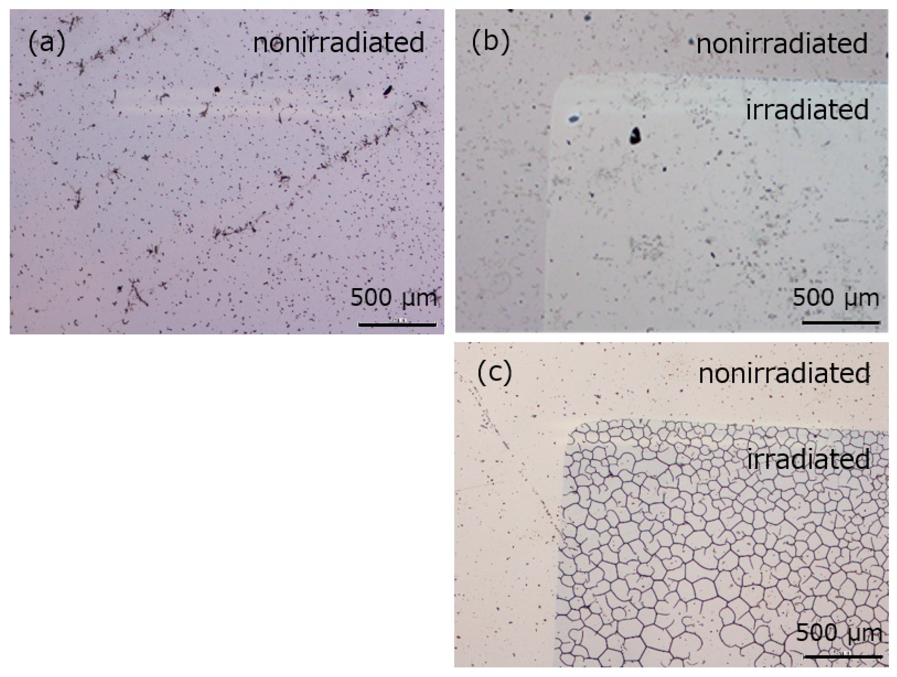
The sample surface before and after F2 laser irradiation was observed with an optical microscope. The results are shown in Figure 2. Figure 2a is a micrograph before laser irradiation, and Figure 2b is a micrograph after laser irradiation for 90 min. As shown in Figure 2b, an optical change on reflection was observed in the laser irradiated area. No such optical change was observed at laser irradiation times of 15 and 60 min. Thus, observation by AFM was performed to confirm whether a step occurred at the boundary between the laser irradiated area and the nonirradiated area. As a result, a clear step could not be measured. Therefore, it can be determined that the optical change in the laser irradiated area is not due to physical material removal such as laser ablation. Additionally, no change in surface roughness was observed between the laser irradiated area and the nonirradiated area.
However, when the sample irradiated with the laser for 90 min was placed in a plastic case for one month, a fine network-like structure was observed only in the laser irradiated area, as shown in Figure 2c. Figure 3 shows the SEM image of a part of the formed network-like structure. As shown in the image, it was confirmed that the carbon thin film surface, which had been flat over the entire irradiation area, was subdivided into polygonal areas. Additionally, judging from the focal position under an optical microscope, it was found that the outline of the polygon, micron-sized reticulated structure was relatively swollen.
Thus, the change in the chemical bonding state between the laser irradiated area and the nonirradiated area was analyzed by Raman spectroscopy. As shown in Figure 4, the nonirradiated carbon thin film exhibited a broad spectrum with a peak around 1530 cm−1. Although there is no clear shoulder around 1400 cm−1 in this spectrum, the nonirradiated sample is considered to have a structure of diamond-like carbon, which is a type of amorphous carbon [23]. No change was also observed in the Raman spectrum after irradiation with F2 laser for 90 min. On the other hand, as mentioned above, one month after laser irradiation, a micron-sized reticulated structure was observed only in the irradiated area, but the Raman spectrum even in this subdivided flat area was almost the same as the nonirradiated spectrum. However, on the reticulated structure, the spectral shape changed remarkably, and a Raman spectrum with two peaks near 1360 and 1580 cm−1 was obtained. They are D-line (1320–1380 cm−1) and G-line (1520–1600 cm−1), attributed to the breathing mode of graphitic clusters and to the stretching of C=C bonds, respectively [24]. Generally, in the Raman spectra of carbon materials, a highly oriented pyrolytic graphite (HOPG) shows a single sharp Raman band at 1581 cm−1. When the structure is disturbed and the crystallite size becomes smaller to approximately 20 nm, a new Raman band is observed near 1360 cm−1 as a pyrolytic graphite (PG). In glassy carbon (GC), where the structure is further disturbed and the crystallite size becomes much smaller to approximately 2 nm, the Raman band near 1580 cm−1 shifts to higher wavenumbers. In addition, the width of the Raman band tends to widen [25]. However, the crystallinity cannot be assessed only by Raman spectroscopy. This should either be revised or supplemented by electron diffraction or by the crystallite size estimation via modern interpretations of Tuinstra–Koenig law [26,27]. Moreover, to identify the formed reticulated structure as a specific type of carbon, it is necessary to indicate not only the peak positions of the D-line and G-line but also the ID/IG ratio and their FWHM with good reproducibility. At present, Raman spectra cannot be measured at all points of the reticulated structure, and even now there are variations in the ID/IG ratio and FWHM. Thus, it is considered that the swelled area of the reticulated structure might be graphitized to have carbon nanocrystals. Generally, in research on structural change of carbon thin films by laser, it is necessary to set the single pulse fluence of lasers to approximately 1 J/cm2 and over, based on the thermal melting process [28,29]. Therefore, this work can be considered as a structural change by a mechanism different from the conventional one.
The formation mechanism of the micron-sized reticulated structure can be qualitatively considered as follows. When an amorphous carbon thin film is irradiated with a low single pulse fluence of F2 laser, photoexcitation at high density occurs on the surface of the carbon thin film, and active oxygen atoms are generated by photodecomposition of oxygen molecules in the atmosphere. The high density means that due to the short wavelength of the F2 laser, the optical absorption coefficient of the material is generally high; the laser penetration depth is short, and many photons are absorbed in the thin surface layer. Thus, it is believed that the carbon atoms in the thin film react with active oxygen atoms and photochemically remove the carbon atoms to be CO or CO2. However, the quantum yield of the photochemical removal may be low. In addition, the depth might be estimated to be approximately 10 nm or less [15]. Thus, no clear step occurs. Then, density change occurs in the laser irradiated area, and an optical change is observed. It is thought that the stress generated in the thin film due to lowering the film density causes the micron-sized reticulated structural change gradually; the reticulated structure may have been graphitized under compressive stress. The possibility of high absorption of carbon in the VUV range could lead to surface oxidation and stress creation during photoexcitation with 157 nm, and stress normalization upon surface cooling can be also expressed. In fact, when a three-slit photomask with a width of 100 µm and a length of 1 mm was used, no reticulated structure was observed even one month after laser irradiation, as shown in Figure 5. This is because smaller mask apertures can significantly reduce the stress induced in the thin film [30]. The reason why it takes one month for the micron-sized reticulated structure to appear is not understood at present. On the other hand, one month is not a threshold time but means that the phenomenon appears with good reproducibility if it is one month at the latest. In addition, by irradiating the F2 laser again on the sample surface on which the reticulated structure is formed, it is possible to reproduce or increase the micron-sized reticulated structure. The present results indicate the possibility of forming a micron-sized reticulated structure composed of carbon nanocrystals in an amorphous carbon thin film with a uniform structure, which can further expand the applications of carbon materials. Moreover, if the density change of the carbon thin film can be increased by the F2 laser, it is suggested that a larger stress could be generated, and a larger carbon crystal might be obtained.
4. Conclusions
The amorphous carbon thin films were irradiated with the F2 laser with the wavelength of 157 nm at the low single pulse fluence of 10 mJ/cm2. It was found that the micron-sized reticulated structural change occurred and caused the network-like swelling structure. Moreover, the reticulated structure was graphitized and is believed to contain carbon nanocrystals. This is because the amorphous carbon thin film was photoexcited at high density by the F2 laser, and the active oxygen atoms were preferentially generated by the photodecomposition of atmospheric oxygen molecules. It is believed that part of the carbon atoms has been photochemically removed. As a result, it can be inferred that the density change of the thin film was induced, and the optical change was observed. It is considered that the stress generated in the thin film due to the density change causes the micron-sized reticulated structural change. The results obtained in the present work are expected to lead to the development of new possibilities for carbon materials by forming the micron-sized reticulated structures in amorphous carbon thin films with a uniform structure. In the future, if it is possible to give a higher density change in the carbon thin film by F2 laser, we may be able to obtain larger carbon crystals on micron-sized reticulated structure.
Funding
This work was supported by JSPS KAKENHI, grant number JP21K04732.
Data Availability Statement
The data that support the findings of this study are available from the corresponding author, M.O., upon reasonable request.
Acknowledgments
The author acknowledges Hiroki Ono and Kaede Iwasaki, National Defense Academy, for helpful assistance and valuable discussion.
Conflicts of Interest
The authors declare no conflict of interest.
References
- Yoon, H.; Liu, P.; Park, Y.; Choi, G.; Choi, P.-P.; Sohn, H. Pulsed laser-assisted additive manufacturing of Ti-6Al-4V for in-situ grain refinement. Sci. Rep. 2022, 12, 22247. [Google Scholar] [CrossRef]
- Chakraborty, S.; Park, H.-Y.; Ahn, S.I. Copper laser patterning on a flexible substrate using a cost-effective 3D printer. Sci. Rep. 2022, 12, 21149. [Google Scholar] [CrossRef]
- Ródenas, A.; Gu, M.; Corrielli, G.; Paiè, P.; John, S.; Kar, A.K.; Osellame, R. Three-dimensional femtosecond laser nanolithography of crystals. Nat. Photonics 2019, 13, 105–109. [Google Scholar] [CrossRef] [Green Version]
- Xu, X.; Wang, T.; Chen, P.; Zhou, C.; Ma, J.; Wei, D.; Wang, H.; Niu, B.; Fang, X.; Wu, D.; et al. Femtosecond laser writing of lithium niobate ferroelectric nanodomains. Nature 2022, 609, 496–501. [Google Scholar] [CrossRef] [PubMed]
- Suttmann, O.; Obata, K.; Nakajima, Y.; Hohnholz, A.; Koch, J.; Terakawa, M.; Overmeyer, L. UV laser photo-polymerization of elastic 2D/3D structures using photo-curable PDMS (Polydimethylsiloxane). J. Laser Micro. Nanoeng. 2017, 12, 153–158. [Google Scholar] [CrossRef] [Green Version]
- Zazo, R.; Solis, J.; Sanchez-Gil, J.A.; Ariza, R.; Serna, R.; Siegel, J. Deep UV laser induced periodic surface structures on silicon formed by self-organization of nanoparticles. Appl. Surf. Sci. 2020, 520, 146307. [Google Scholar] [CrossRef]
- Meinertz, J.; Fricke-Begemann, T.; Ihlemann, J. Micron and sub-micron gratings on glass by UV laser ablation. Physica. Procedia. 2013, 41, 708–712. [Google Scholar] [CrossRef] [Green Version]
- Iwasaki, K.; Yoshida, T.; Okoshi, M. Near-superhydrophobic silicone microcapsule arrays encapsulating ionic liquid electrolytes for micro-power storage assuming use in seawater. Sci. Rep. 2022, 12, 18264. [Google Scholar] [CrossRef]
- Takao, H.; Okoshi, M.; Inoue, N. Fabrication of SiO2-humps on silicone rubber using F2 laser. Jpn. J. Appl. Phys. 2002, 41, L1088–L1089. [Google Scholar] [CrossRef]
- Okoshi, M.; Kimura, T.; Takao, H.; Inoue, N.; Yamashita, T. Photochemical modification of silicone films using F2 laser for selective chemical etching. Jpn. J. Appl. Phys. 2004, 43, 3438–3442. [Google Scholar] [CrossRef]
- Okoshi, M.; Li, J.; Herman, P.R. 157-nm F2-laser writing of silica optical waveguides in silicone rubber. Opt. Lett. 2005, 30, 2730–2732. [Google Scholar] [CrossRef]
- Nojiri, H.; Okoshi, M. Surface texturing effect on crack suppression of SiO2 film formed by F2 laser-induced photochemical surface modification of silicone on polycarbonate under heat resistance test. Jpn. J. Appl. Phys. 2017, 56, 085502. [Google Scholar] [CrossRef]
- Okoshi, M.; Awaihara, Y.; Yamashita, T.; Inoue, N. F2 laser induced surface modification of iron thin films to obtain corrosion resistance. Jpn. J. Appl. Phys. 2014, 53, 022702. [Google Scholar] [CrossRef]
- Okoshi, M.; Awaihara, Y.; Yamashita, T.; Inoue, N. Fabrication of hydrophobic and corrosion resistant iron thin film by interference exposure using 157 nm F2 laser. Mater. Lett. 2015, 139, 300–302. [Google Scholar] [CrossRef]
- Okoshi, M.; Iwai, K.; Nojiri, H.; Inoue, N. F2 laser induced modification of aluminum thin films into transparent aluminum oxide. Jpn. J. Appl. Phys. 2012, 51, 122701. [Google Scholar] [CrossRef]
- Losero, E.; Jagannath, S.; Pezzoli, M.; Goblot, V.; Babashah, H.; Lashuel, H.A.; Galland, C.; Quack, N. Neuronal growth on high-aspect-ratio diamond nanopillar arrays for biosensing applications. Sci. Rep. 2023, 13, 5909. [Google Scholar] [CrossRef] [PubMed]
- Stoddart, A. Fullerenes make connections. Nat. Synth. 2023, 2, 78. [Google Scholar] [CrossRef]
- Tian, H.; Ma, Y.; Li, Z.; Cheng, M.; Ning, S.; Chen, J.; Zhou, W.; Liu, L.; Wang, E.; Pei, J.; et al. Disorder-tuned conductivity in amorphous monolayer carbon. Nature 2023, 615, 56–61. [Google Scholar] [CrossRef]
- Ban, M.; Chen, J. Fabrication of plane-type axon guidance substrates by applying diamond-like carbon thin film deposition. Sci. Rep. 2023, 13, 8489. [Google Scholar] [CrossRef] [PubMed]
- Wang, X.; Zhang, X.; Wang, C.; Lu, Y.; Hao, J. High temperature tribology behavior of silicon and nitrogen doped hydrogenated diamond-like carbon (DLC) coatings. Tribol. Int. 2022, 175, 107845. [Google Scholar] [CrossRef]
- Jang, Y.-J.; Kim, J.-I.; Lee, W.-Y.; Kim, J. Friction properties of thick tetrahedral amorphous carbon coating with different surface defects under dry contact conditions. Appl. Surf. Sci. 2023, 550, 149332. [Google Scholar] [CrossRef]
- Lai, C.Q.; Lim, G.Y.; Tai, K.J.; Lim, K.J.D.; Yu, L.; Kanaujia, P.K.; Seetoh, P.I. Exceptional energy absorption characteristics and compressive resilience of functional carbon foams scalably and sustainably derived from additively manufactured kraft paper. Addit. Manuf. 2022, 58, 102992. [Google Scholar] [CrossRef]
- Yoshikawa, M. Raman spectra of diamondlike amorphous carbon films. Mater. Sci. Forum. 1990, 52–53, 365–386. [Google Scholar]
- Streletskiy, O.A.; Zavidovskiy, I.A.; Balabanyan, V.Y.; Tsiskarashvili, A.V. Antibacterial properties of modified a-C and ta-C coatings: The effects of the sp2/sp3 ratio, oxidation, nitridation, and silver incorporation. Appl. Phys. A 2022, 128, 929. [Google Scholar] [CrossRef]
- Nemanich, R.J.; Solin, S.A. First- and second-order Raman scattering from finite-size crystals of graphite. Phys. Rev. B 1979, 20, 392–401. [Google Scholar] [CrossRef]
- Zickler, G.A.; Smarsly, B.; Gierlinger, N.; Peterlik, H.; Paris, O. A reconsideration of the relationship between the crystallite size La of carbons determined by X-ray diffraction and Raman spectroscopy. Carbon 2006, 44, 3239–3246. [Google Scholar] [CrossRef]
- Mallet-Ladeira, P.; Puech, P.; Toulouse, C.; Cazayous, M.; Ratel-Ramond, N.; Weisbecker, P.; Vignoles, G.L.; Monthioux, M. A Raman study to obtain crystallite size of carbon materials: A better alternative to the Tuinstra–Koenig law. Carbon 2014, 80, 629–639. [Google Scholar] [CrossRef]
- Zkria, A.; Haque, A.; Egiza, M.; Abubakr, E.; Murasawa, K.; Yoshitake, T.; Narayan, J. Laser-induced structure transition of diamond-like carbon coated on cemented carbide and formation of reduced graphene oxide. MRS Commun. 2019, 9, 910–915. [Google Scholar] [CrossRef]
- Kudryashov, S.I.; Karabutov, A.A.; Kudryashova, M.A.; Beketov, V.I.; Zorov, N.B. Laser-induced phase transitions of carbon. Mendeleev. Commun. 1998, 8, 29–30. [Google Scholar] [CrossRef]
- Nojiri, H.; Okoshi, M. Crack suppression of silica glass formed by zoned F2 laser-induced photochemical surface modification of hard silicone thin film coating on polycarbonate. Jpn. J. Appl. Phys. 2016, 55, 122701. [Google Scholar] [CrossRef]
Figure 1.
Schematic drawing of the experimental setup.

Figure 2.
Optical micrographs of the carbon thin films: (a) before F2 laser irradiation; (b) after F2 laser irradiation; (c) one month after F2 laser irradiation.
Figure 2.
Optical micrographs of the carbon thin films: (a) before F2 laser irradiation; (b) after F2 laser irradiation; (c) one month after F2 laser irradiation.

Figure 3.
SEM image of the formed micron-sized reticulated structure.

Figure 4.
Raman spectra of the carbon thin films before and after F2 laser irradiation.

Figure 5.
Optical micrographs of the carbon thin films: (a) after F2 laser irradiation; (b) one month after F2 laser irradiation.
Figure 5.
Optical micrographs of the carbon thin films: (a) after F2 laser irradiation; (b) one month after F2 laser irradiation.

Disclaimer/Publisher’s Note: The statements, opinions and data contained in all publications are solely those of the individual author(s) and contributor(s) and not of MDPI and/or the editor(s). MDPI and/or the editor(s) disclaim responsibility for any injury to people or property resulting from any ideas, methods, instructions or products referred to in the content. |
© 2023 by the author. Licensee MDPI, Basel, Switzerland. This article is an open access article distributed under the terms and conditions of the Creative Commons Attribution (CC BY) license (https://creativecommons.org/licenses/by/4.0/).
Share and Cite
MDPI and ACS Style
Okoshi, M. F2 Laser-Induced Micro-Reticulated Structural Changes of Amorphous Carbon Thin Films. Micro 2023, 3, 602-609. https://doi.org/10.3390/micro3020041
AMA Style
Okoshi M. F2 Laser-Induced Micro-Reticulated Structural Changes of Amorphous Carbon Thin Films. Micro. 2023; 3(2):602-609. https://doi.org/10.3390/micro3020041
Chicago/Turabian StyleOkoshi, Masayuki. 2023. "F2 Laser-Induced Micro-Reticulated Structural Changes of Amorphous Carbon Thin Films" Micro 3, no. 2: 602-609. https://doi.org/10.3390/micro3020041