Article

Pt and Pd Nanoparticle Crystallization in the Sol-Gel-Derived Thin SiO2 Films

1
Petersburg Nuclear Physics Institute of National Research Centre “Kurchatov Institute”, 188300 Gatchina, Russia
2
Institute of Silicate Chemistry of Russian Academy of Sciences, 199034 Saint-Petersburg, Russia
3
Ioffe Institute, 194021 Saint-Petersburg, Russia
4
Saint Petersburg Electrotechnical University “LETI”, 197376 Saint-Petersburg, Russia
*
Author to whom correspondence should be addressed.
Physchem 2023, 3(2), 259-269; https://doi.org/10.3390/physchem3020018
Submission received: 27 February 2023 / Revised: 29 May 2023 / Accepted: 12 June 2023 / Published: 15 June 2023
(This article belongs to the Section Nanoscience)

Abstract

:
The crystallization and distribution the features of Pt, Pd and Pt/Pd nanoparticles in spin-on glass SiO2 films were studied within a wide range of the dopant concentrations in silica sol (from 10 to 80 mol.% Pt, Pd or Pt/Pd per 100 mol.% Si). The grazing incidence X-ray diffraction (GIXRD) characterization revealed that the formation of 4–8 nm sized crystalline Pt, Pd and Pt/Pd nanoparticles in SiO2 films began at the dopant concentrations of at least 10 mol.% Pt and/or Pd per 100 mol.% Si. The nanoparticles obtained from sols with the lower Pt, Pd or Pt/Pd concentrations were characterized by an amorphous structure. The dopants distribution over the film thickness (~21–47 nm) was studied using X-ray reflectometry. The effect of the dopant concentration, spin-coating modes and heat treatment temperature on the film thickness was characterized. When only one of the dopants (Pt or Pd) was introduced into the silica sol, the resulting nanoparticles were preferentially localized close to the film surface. When dopants were used together, the Pt/Pd nanoparticles were distributed more evenly.

1. Introduction

Spin-on glass films of SiO2, TiO2 and ITO doped with various elements (B, Pt, Pd, Nb, etc.) are used in microelectronics and photonics, e.g., as diffuse emitters for semiconductor materials in the manufacture of solar cell modules [1,2], and optical and semiconductor sensors with improved performances [3,4,5]. Thus, such dopants are usually distributed in SiO2 or TiO2 film-forming matrices obtained from sols in the form of micro- or nanoscale interpenetrating phases [6] or nanoparticles [7,8,9,10]. The size, morphology and phase composition of these nanoparticles and their distribution in the film significantly affect the target (optical, catalytic, etc.) properties of the spin-on glass films. The process of silica film formation is determined by the rheological properties of a sol and the conditions when it is coated on a substrate. The rheological properties of the sol are determined by the precursor concentrations, the nature of the solvents, the sol aging time and other factors. The structure and thickness of the obtained film is determined by spin-coating modes: the temperature of the applied sol, the rotation speed and temperature of the substrate, as well as the temperature of the subsequent heat treatment of the film. Therefore, research to establish the patterns between the technological modes of spin-on glass film production with specified properties and their structure is of particular interest.
The characterization of the structure and composition of nanosized (thickness about 30–100 nm) films, such as spin-on glass films, is quite complicated and requires the use of a complex set of research methods. In our earlier studies, catalytically active “spin-on glass” silica films were synthesized using a sol-gel method [11,12]. The results of our studies showed that the films doped with Pt nanoparticles, obtained from sols aged for 6 years, were 1.5–2 times thicker than the films obtained from the sols aged for 1 week. Various temperature modes were used: increasing the annealing temperature led to a decrease in the film thickness and an increase in the electron density [12]. The study of the Pt/Pd nanoparticle crystal structure in silica films and xerogels showed that they are formed as crystallites with a common mixed-alloy-type lattice. The lattice parameters in such crystallites depend on the ratio of Pt and Pd in the initial sol. The crystallite size was 5–6 nm in the films and 10–17 nm in the xerogels obtained under identical technological conditions from the same sol [13].
In this research work, to study the film formation and crystallization of SiO2 thin films depending on the wide range changes in the concentration of dopants (Pt and Pd compounds) in silica sols and spin-coating modes, a set of research methods—grazing incident diffraction of X-ray (GiXRD), X-ray reflectometry (XRR) and transmission electron microscopy (TEM)—was used. Subsequently, the applied research methods can be extended to other “spin-on glass” films obtained from various precursors (primarily silicon alkoxides and other compounds) containing different dopants.

2. Materials and Methods

2.1. Chemicals

Tetraethoxysilane Si(OC2H5)4 (TEOS), hexachloroplatinic (IV) acid hexahydrate H2PtCl6·H2O and palladium (II) chloride PdCl2 were used as the sol precursors. Hydrochloric acid solution (37 wt.%), ethanol (96 wt.%.), butanol-1 and distilled water were also used in the synthesis. All the reactants were of reagent-grade purity and used without further purification.

2.2. Silica Sol Synthesis and Spin-On Glass Film Formation

The sols were obtained according to the procedure developed in our earlier studies and described in detail in [11,13]. The ratios between the components (platinum, palladium and silica) in the solution (mol.%) are shown in Table 1. During all syntheses, TEOS was used as a precursor in the content 3 vol.%. The sols were spin-coated onto a single-crystal silicon wafer (pre-cleaned in alcohol solutions) at the spinning rates of 500, 1500 or 2500 rpm for 45 s, followed by heat treatment at Ta = 100, 130, 250, 500 °C for 30 min in air.
An identification of the samples, for example “5Pt_5Pd_100Si_250”, means that the film was prepared from the sol with the component ratio (in mol.%) of 5Pt:5Pd:100Si, and dried at the temperature of 250 °C.

2.3. Characterization

The phase composition of Pt, Pd or Pt/Pd-containing silica films was determined using the grazing incidence X-ray diffraction (GIXRD) method, using a Rigaku SmartLab diffractometer (CuKα, 45 kV, 200 mA) with in-plane geometry, involving a quasi-parallel X-ray beam formed by a parallel-slit collimator and an incident on the sample surface at a fixed grazing angle ω = 1 deg. The detector was rotated around the φ-axis, rectangular to the plane of the sample surface, also rotating around the same axis.
The film thickness and roughness were determined via X-ray reflectometry (XRR) measurements using the Rigaku SmartLab diffractometer in the quasi-parallel X-ray beam mode. The reflectivity curves were recorded at ω/2θ geometry with a step of ω = 0.005°.
The distribution of Pt, Pd or Pt/Pd nanoparticles in the prepared silica films was studied via transmission electron microscopy (TEM) using a Jeol JEM-2100F microscope (accelerating voltage 200 kV, point resolution 0.19 nm). The samples for TEM characterization were prepared by depositing the studied material onto a conventional copper TEM grid coated with a lacey carbon film.

3. Results and Discussion

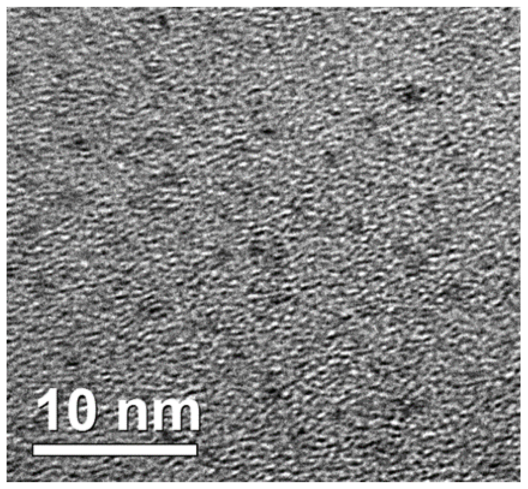
3.1. Surface Morphology

Straight after placing a sol drop onto the rotating substrate and the formation of the film, its surface condition (continuity and homogeneity) was visually assessed according to the appearance of “Newton rings”. If the concentration of the metal salts in the sol is too high, the films are formed with defects called “comets”. Based on the visual assessment, the acceptable range of Pt and Pd concentrations in the sols was established and ranged from 5 to 80 mol.% Me (Pt, Pt/Pd, Pd) per 100 mol.% Si. At Me contents higher than 80 mol.%, the surface of the obtained films was non-uniform, involving “comet” defects. The surface morphology of the films obtained at dopant concentrations (Pt, Pd or Pt/Pd) less than 5 mol.% per 100 mol.% Si was described in detail in our previous studies [11,12].

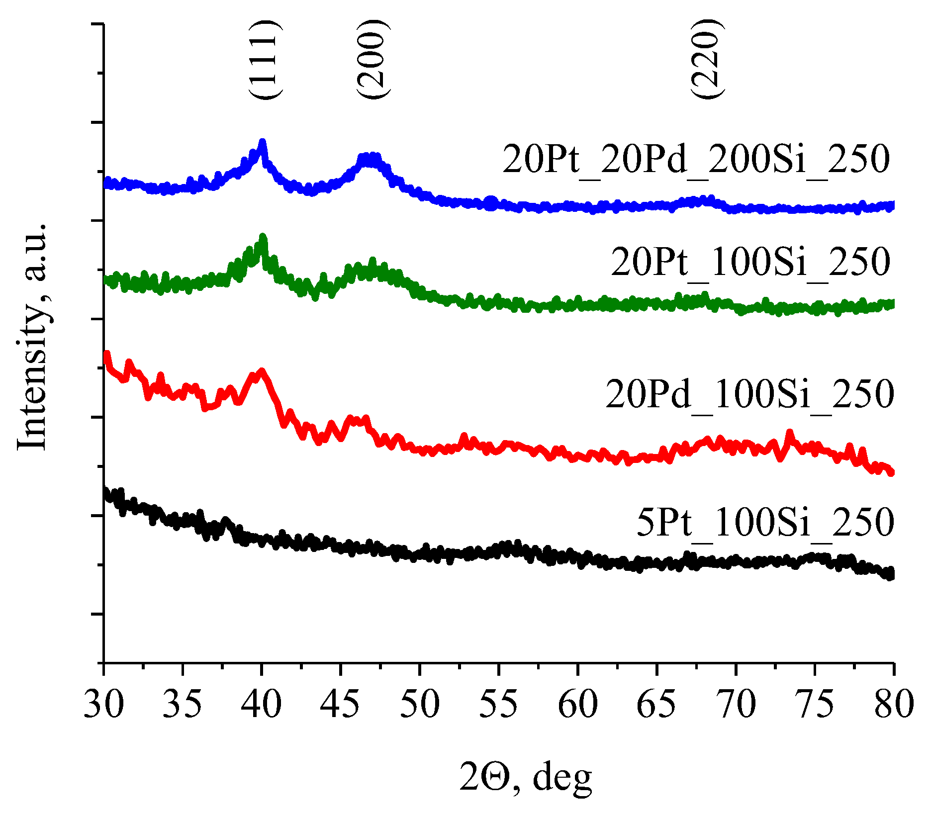
3.2. Phase Composition of Silica Films Doped with Pt and Pd

In the XRD profiles of the films with the lowest Pt or Pd content (5 mol. per 100 mol.% Si), no diffraction peaks were observed, indicating the crystalline structure (Figure 1, Table 2). For the films with higher Pt or Pd concentrations (10 mol.% per 100 mol.% Si and higher), the peaks corresponding to a face-centered cubic (FCC) Pt or Pd lattice appear in the XRD profiles.
In order to study the possible «nucleation» of crystallites, the sol (5Pt_5Pd_100Si) was coated as a film onto a Cu mesh, followed by air-drying first at an ambient temperature. Then, the film was treated additionally at 130 °C for 1 h with thermostat in air until the complete removal of solvents and residual organic substances.
Figure 2 shows a TEM image of this film, indicating the formation of 1–2 nm sized metal nanoparticles in the silica matrix (5Pt_5Pd_100Si_130). The parameter of the Pt/Pd lattice is a = 3.896 Å, indicating that the size of metal nanoparticles is only about 3–5 lattice periods. Nanoparticles of such a small size cannot have a regular crystal structure and can be characterized as crystal embryos with an amorphous structure.
The average crystallite size was determined from the peak width of Bragg peaks (111) of the FCC lattice. For this purpose, additional measurements were made near the Bragg peak (111), in the angle range of 35–45°, with the step of 0.01° and large exposure for the intensity measurement at each point. The SCR values of the Pt/Pd nanoparticles calculated using the Scherrer equation are summarized in Table 2 [14].
Although no clear correlation is found between the average crystallite size and dopant content in the samples containing Pd and Pt/Pd nanoparticles, the average crystallite size of the films containing Pt nanoparticles is directly proportional to their Pt content.

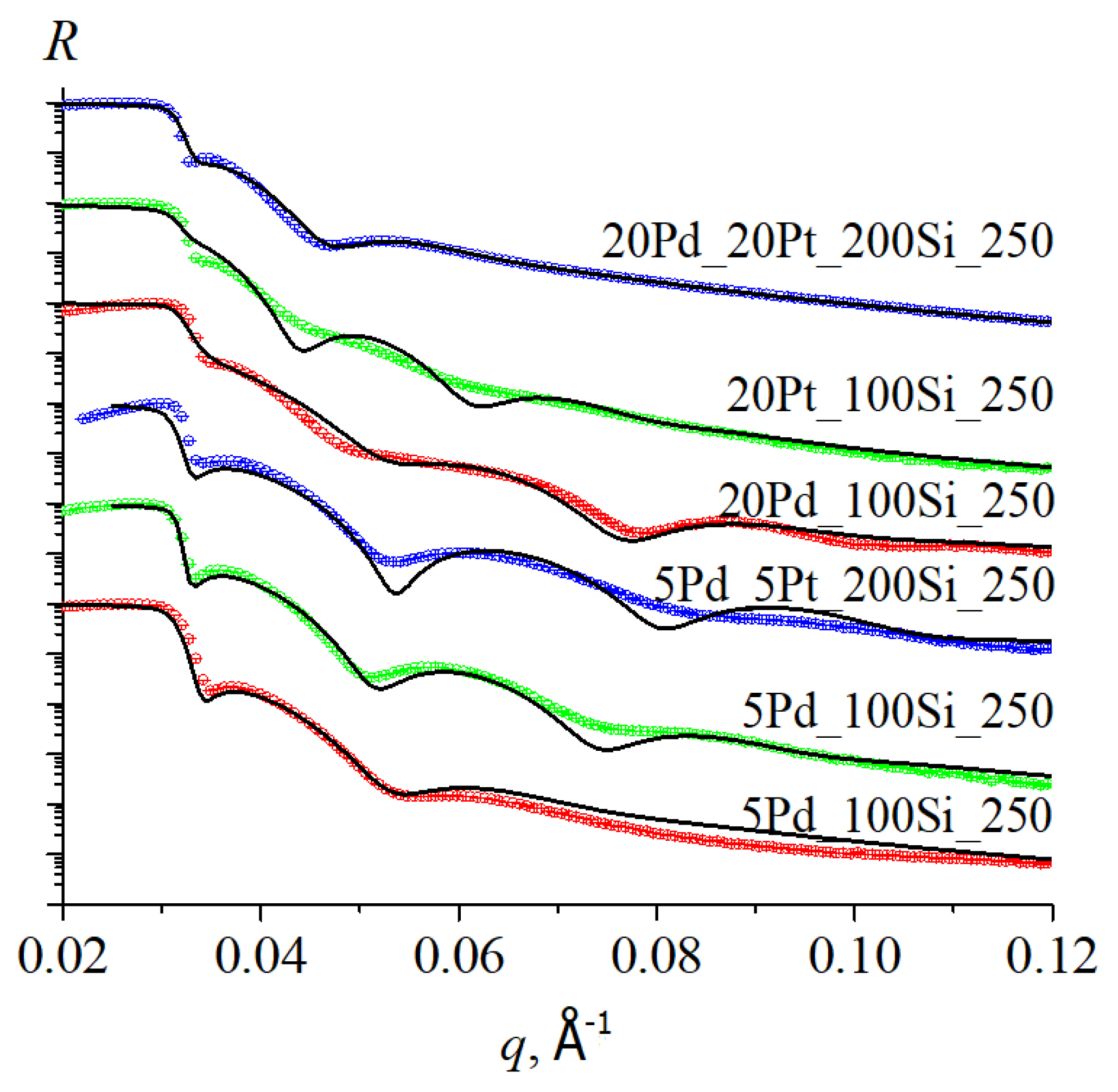
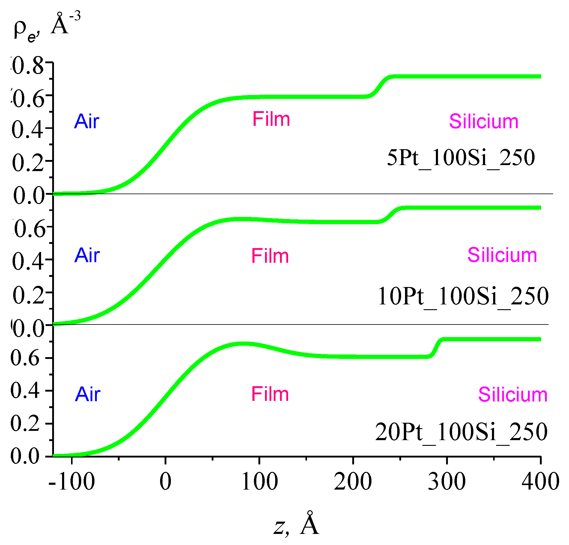
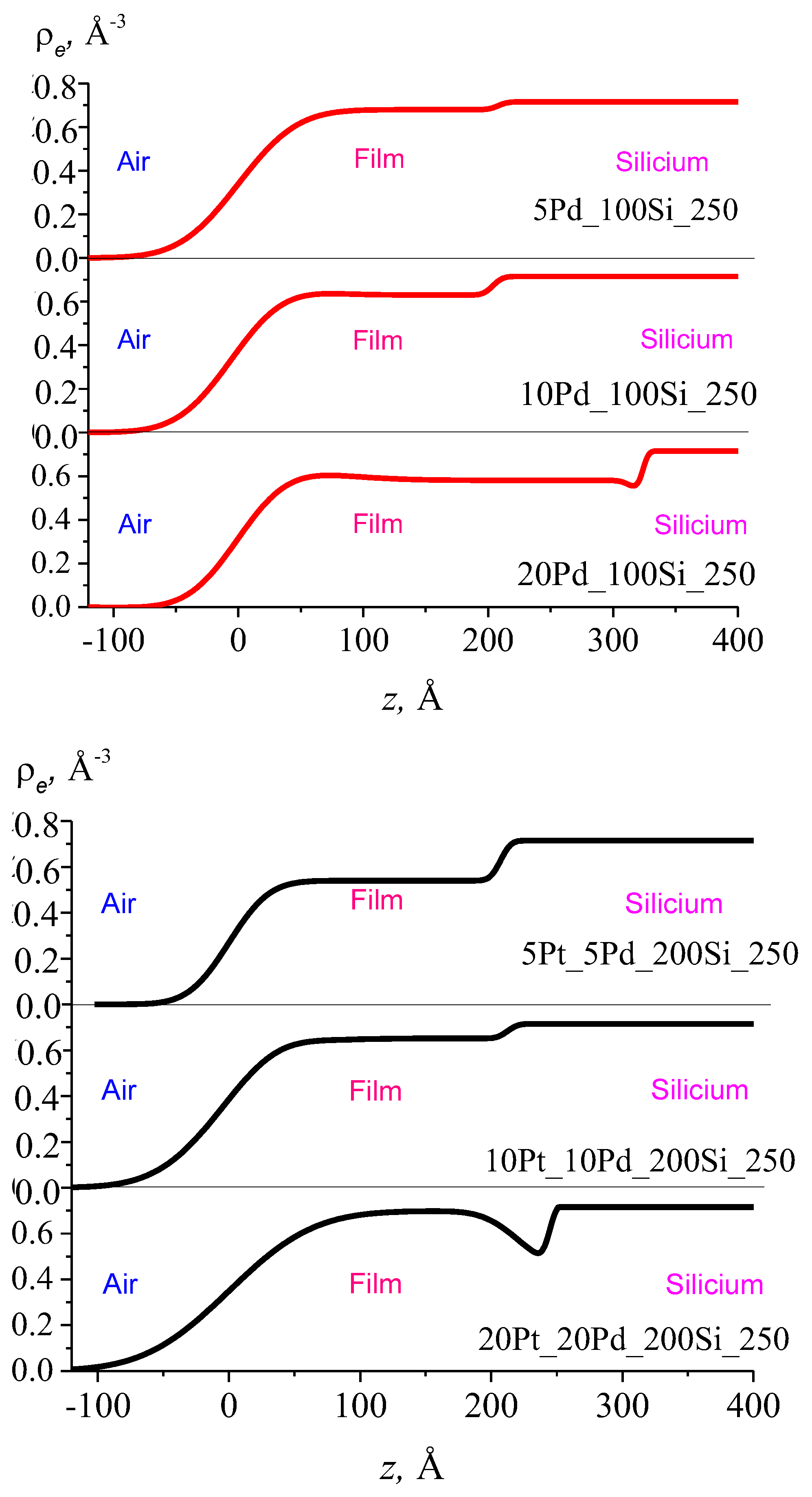
3.3. Thickness Profile of Silica Films Doped with Pt/Pd

Figure 3 shows examples of XRR plots for the studied samples. The oscillation period of the X-ray reflection coefficient R, depending on the transmitted wave vector q, is inversely proportional to the film thickness, and the oscillation attenuation provides information about the roughness value of the sample surface σ. The reflectometric curves, R(q), were calculated using the Motofit software package, allowing for the calculation of reflection coefficients of X-rays from thin films and multilayer systems [15].
To fit the reflectometric curves obtained for the films with low metal concentrations (5 mol. per 100 mol. Si), a film model with a uniform thickness of electron density, ρe, was used. This model approximation gave a good agreement between the calculated and experimental R(q) curves. However, in order to satisfactorily describe the reflection from the samples with the higher metal concentrations, it was necessary to complicate the model by introducing the electron density gradient along the film depth z (Figure 4). For the samples with nanoparticles of a single dopant (Pt or Pt), the electron density maximum was observed near the surface of the films, while for the films containing mixed Pt/Pd nanoparticles, the electron density maximum was closer to the middle of their thickness.
Since the reflectometric curves of the films 40Pt_100Si, 80Pt_100Si, 40Pd_100Si and 80Pd_100Si were significantly smoothed due to an intensive off-specular X-ray scattering, it was impossible to determine their parameters from XRR data.
The higher concentration of the metal nanoparticles near the surface of the obtained films has the important practical application as the basis of hydrogen sensors. In our previous work [16], the silica films containing Pd nanoparticles were coated onto the InP substrate by spin-coating at room temperature and a substrate rotation frequency of ~1700 rpm; after that, they were heat-fixed at 130 °C with a thermostat for 50 min. The thickness of the synthesized films, according to X-ray reflectometry data, was d = 46.8 ± 0.3 nm, and the size of the DCSR nanoparticles was ~8 nm. The measurement of the current-voltage characteristics of the InP/Pd thin-film structures showed a decrease in the cut-off voltage in the presence of hydrogen. Previously, for hydrogen-sensitive Pd/n-InP Schottky diodes, it was observed that by illuminating the structure with a LED (λ = 0.9 µm) and an impulse exposure to hydrogen, the photovoltage and photocurrent changed.
The increase in the electron density near the upper boundaries of the silica films doped with only Pt or Pd nanoparticles indicates that in these samples the metal particles are concentrated mainly near the surface. A similar distribution of metal nanoparticles has been observed previously in the silica films containing Pt nanoparticles [12]. The predominant concentration of the metallic nanoparticles was then established from a combination of X-ray reflectometry and Rutherford backscattering (RBS) data.
Table 3 shows the parameters of the studied films determined from fitting the corresponding reflectivity curves. The range of the film thickness varies from 20 to 32 nm, increasing with the concentration of metallic nanoparticles. The value of the maximum electron density also correlates with the content of the Pt, Pd or Pt/Pd nanoparticles.
For the samples with low metal concentrations (5 mol. per 100 mol. Si), it is possible to calculate the value of their porosity according to the electron density, ρe, obtained using X-ray reflectometry data of the single-layer model. The average mass density of the film can be calculated using the electron density value obtained from experimental data. The density of a known pore-free material can be calculated by:
ρ = i x i ρ i
where xi is the component fraction (Pt, Pd or SiO2) in the material, ρi is the density of the component, and the density of platinum ρ(Pt) = 21.44 g/cm3; palladium ρ(Pd) = 12.02 g/cm3 and amorphous silicon dioxide ρ(SiO2) = 2.2 g/cm3.
The porosity value, P, can be estimated by:
P = ( 1 ρ e x p ρ ) · 100 %
The average measured sample density and porosity values are shown in Table 4.
The table shows that the porosity of the films containing Pt and Pt/Pd nanoparticles is approximately twice as high as the one containing only Pd nanoparticles. It can be assumed that this is due to the fact that Pt nanoparticles contribute actively to the formation of agglomerates in the films.

3.4. Effect of the Synthesis Conditions on the Film Thickness

A simplified model describing the effect of spin-coating process parameters on the prepared film thickness was proposed by Meyerhofer in [17] and further developed by Bornside et al. [18,19]. It should be noted that, according to the model approximations, both the stages of sol coating on the substrate and solvent evaporation are sequential and run independently to each other. According to this model, the thickness of a spin-coated film is described by the equation:
d = ( 1 x 0 ) [ 3 η 0 p M k x 0 2 ρ 0 2 ω 2 R T ] 1 / 3 ,
where x0 is the initial concentration of the solvent, η0 and ρ0 are the viscosity and density of the applied sol spin-coated, respectively, p and M are the vapor pressure and molecular weight of the solvent, respectively, R is the universal gas constant and T is the temperature.
The mass transfer coefficient k is defined by the expression:
k = c D ( ω / ν ) 1 / 2 ,
where c is a constant determined by the Schmidt number, D is the diffusion coefficient of the solvent molecules in air and ν is the kinematic viscosity of the gas layer above the sample surface.
Thus, it follows from the model approximations that the film thickness is d ~ ω 1 / 2 . According to experimental studies of various sols, the dependence of the thickness of the obtained films on the rotation frequency is estimated as d ~ ω λ , where the power degree λ varies from 0.45 to 1.40, but in most cases for silica sols, the index λ is close to 0.5.
The thicknesses of the 20Pt_100Si_250 films obtained at different substrate rotation frequencies are shown in Figure 5. In the interval of rotation frequency ω ϵ [1500, 2500] rpm, the experimental points are well fitted by the d ~ ω λ law, with the index λ = 0.68 ± 0.04. At the substrate rotation frequency ω = 1000 rpm, the film thickness no longer follows the power law d ~ ω 0.68 ± 0.04 . The effect of the substrate rotation speed on the film formation process will be the subject of additional studies in the future.
The deviation of the index λ from 0.5 can be explained by the fact that the model proposed by Meyerhoffer does not take into account the porosity of the films and the presence of any nanoparticles in the films, assuming that the films are homogeneous and continuous. Although the effect of porosity and nanoparticles on λ is unknown, it can be assumed that they make a contribution to this value, e.g., due to the effect of sol over saturation with platinum and palladium salts upon the solvent evaporation process during the film coating. As shown in [20], the dependence of the deposited film thickness on spin speed likely depends on the nature of the evaporation process. Particularly, if the flux of the evaporated solvent molecules from the surface is proportional to the square root of the rotation rate, then d ~ ω 1 / 2 , while in the case the solvent flux is constant (does not depend on the rotation rate), d ~ ω 3 / 2 , and in the case of hard-to-vaporize solvents, d ~ ω 1 . The change in the dynamics of the evaporation process is mainly due to the formation of a near-surface region with a low solvent concentration (skin layer) and the subsequent formation of a glassy layer during the centrifugation of sol-gel films. These processes are facilitated by the rapid polycondensation of the silica sol. The diffusion of the solvent molecules through such a layer is considerably hindered, resulting in an increased λ index from 0.5 to 1 [20]. The indirect evidence of this hypothesis is the observed concentration of metal nanoparticles near the film surface, since the formation of a dense vitreous layer leads to the increase in the porosity of the lower layer of the forming film, and consequently to a decrease in its density.
Another possible mechanism responsible for the observed increase in the index λ relates to the non-Newtonian rheology of the sol during spin-coating, after reaching a certain critical shear rate. Increasing the sol concentration leads to an increase in the number of aggregates in it and a growth of its viscosity, but these aggregates collapse with the increasing shear rate, and consequently, the sol viscosity of the sol decreases. In turn, the decrease in viscosity leads to an increase in convective centrifugal flow and an increase in the λ index [21,22]. The non-Newtonian rheology of the sol should lead to an increase in film thickness as it moves toward the edge of the sample. However, our measurements showed that the difference between the film thicknesses in the center of the samples and their edge does not exceed 3–5%, even for the samples with a diameter of 50 mm.
To study the effect of heat treatment temperature on the thickness of the obtained films, sols with a metal concentration of 20 mol per 100 mol Si were coated on silicon substrates, with subsequent spin-coating at ω = 2500 rpm, and heated at fixed temperatures Ta = 20–500 °C. Figure 6 shows the thickness of silica films doped with Pt, Pd and Pt/Pd as a function of their heating temperature.
The obtained data show that the thickness of the films decreases with the increasing temperature, Ta, probably due to the film shrinkage and reduction in porosity during heat treatment at fixed elevated temperatures. The slope of the film thickness curve on the heat treatment temperature for the films doped with Pt/Pd nanoparticles is markedly different from that of the dopant Pt or Pd samples. This may be related to the spatial distribution of crystallites and nanoparticles in the films. Crystallites assemble into nanoparticles, which can form spatial agglomerates both on the surface and inside the film. The formation of agglomerates from Pt and Pt/Pd nanoparticles was previously observed in [11,23]. The structure and location of such agglomerates have an influence on the number of pores and their distribution in the silicate film. According to the X-ray reflectometry data, the electron density of the films doped with Pt/Pd nanoparticles is markedly lower than that of the samples doped with only Pt or Pd nanoparticles (Table 3), indicating a greater porosity of these samples. Therefore, annealing such films leads to a significant decrease in porosity and, consequently, an increase in film shrinkage.

4. Conclusions

The spin-coating method allowed for obtaining silica sol thin films doped with platinum-group metal nanoparticles. The thickness of such films depends on the centrifugation modes and the concentration of the dopants distributed in the silica films in the form of Pt, Pd or Pt/Pd nanoparticles. Increasing the spin rate speed leads to a decrease in the thickness of the obtained films, including due to the formation of a near-surface region with a low solvent concentration (skin layer), followed by the formation of a dense vitreous layer significantly hindering the diffusion of solvent molecules. This is indirectly confirmed by the presence of an electron density gradient with an increased concentration of nanoparticles near the upper boundaries of the films, particularly evident in samples with a large Pt, Pd or Pt/Pd content.
The influence of non-Newtonian rheology of doped silica sols on the thickness of the obtained films can be ignored, since direct measurements did not reveal the presence of a significant gradient in a film thickness between the center and the edges of the samples.
An increase in the heat treatment temperature of the films results in a decrease in their thickness that can account for the increase in the porosity of the films during their annealing.
The nanoparticles in the films formed from low-dopant-content sols (5 moles of Pt, Pd or Pt/Pd per 100 moles of Si) are characterized by an amorphous structure. A TEM analysis of the 5Pt_5Pd_100Si_130 film showed the formation of the Pt, Pd or Pt/Pd nanoparticles with the size of 1–2 nm (approximately 3–5 FCC parameters of the Pt/Pd lattice) unable to have a regular crystal structure. Increasing the metal content in the initial sol leads to the formation of nanoparticles containing metal crystallites with an average size of about 4–8 nm. The average crystallite size in silica films containing Pt nanoparticles correlates with the platinum content in the initial sol. However, the average crystallite size in the films doped with Pd and Pt/Pt nanoparticles is almost independent of the concentration of metals in the initial sol.

Author Contributions

Conceptualization, N.G. and V.M.; methodology, N.G.; validation, N.G., V.M. and E.G.; formal analysis, V.M., E.G., D.K. and Y.S.; investigation, N.G., V.M., E.G., D.K. and Y.S.; resources, O.S. and N.G.; writing—original draft preparation, N.G., V.M. and Y.S.; writing—review and editing, N.G., V.M., E.G., D.K. and O.S.; visualization, N.G., V.M. and D.K.; supervision, O.S.; project administration, N.G. All authors have read and agreed to the published version of the manuscript.

Funding

This research received no external funding.

Data Availability Statement

Not applicable.

Acknowledgments

TEM studies were performed using the equipment of the Federal Joint Research Center “Material Science and Characterization in Advanced Technologies”, with the support of the Ministry of Science and Higher Education of the Russian Federation.

Conflicts of Interest

The authors declare no conflict of interest.

References

  1. Dominguez, M.A.; Luna-Lopez, J.A.; Moreno, M.; Orduña, A.; Garcia, M.; Alcantara, S.; Soto, S. Solution-processed transparent dielectric based on spin-on glass for electronic devices. Rev. Mex. De Física 2016, 62, 282–284. [Google Scholar]
  2. Yang, N.; Li, S.; Yang, J.; Li, H.; Ye, X.; Liu, C.; Yuan, X. Avoidance of boron rich layer formation in the industrial boron spin-on dopant diffused n-type silicon solar cell without additional oxidation process. J. Mater. Sci. Mater. Electron. 2018, 29, 20081–20086. [Google Scholar] [CrossRef]
  3. Yanagida, S.; Makino, M.; Ogaki, T.; Yasumori, A. Preparation of Pd–Pt Co-Loaded TiO2 Thin Films by Sol-Gel Method for Hydrogen Gas Sensing. J. Electrochem. Soc. 2012, 159, B845. [Google Scholar] [CrossRef]
  4. Qadri, M.U.; Diaz Diaz, A.F.; Cittadini, M.; Martucci, A.; Pujol, M.C.; Ferré-Borrull, J.; Llobet, E.; Aguiló, M.; Díaz, F. Effect of Pt nanoparticles on the optical gas sensing properties of WO3 thin films. Sensors 2014, 14, 11427–11443. [Google Scholar] [CrossRef] [PubMed] [Green Version]
  5. Nicolescu, M.; Mitrea, D.; Hornoiu, C.; Preda, S.; Stroescu, H.; Anastasescu, M.; Calderon-Moreno, J.M.; Predoana, L.; Teodorescu, V.S.; Maraloiu, V.-A.; et al. Structural, Optical, and Sensing Properties of Nb-Doped ITO Thin Films Deposited by the Sol–Gel Method. Gels 2022, 8, 717. [Google Scholar] [CrossRef]
  6. Shilova, O.A.; Tsvetkova, I.N.; Khamova, T.V.; Angelov, B.; Drozdova, I.A.; Kruchinina, I.Y.; Kopitsa, G.P. Sol-Gel Synthesis and Structure of Nanocomposites Based on Tetraethoxysilane and Boron Compounds. Glass Phys. Chem. 2021, 47 (Suppl. S1), S48–S62. [Google Scholar] [CrossRef]
  7. Bhattacharjee, B.; Ganguli, D.; Chaudhuri, S.; Pal, A.K. ZnS: Mn nanocrystallites in SiO2 matrix: Preparation and properties. Thin Solid Films 2002, 422, 98–103. [Google Scholar] [CrossRef]
  8. Manzanares-Martínez, J.; García-Cerda, L.A.; Ramírez-Bon, R.; Espinoza-Beltran, F.J.; Perez-Robles, J.F.; Gonzalez-Hernandez, J. Stabilization of copper-based colloidal particles in sol–gel SiO2 thin films. Thin Solid Films 2000, 365, 30–35. [Google Scholar] [CrossRef]
  9. Babapour, A.; Akhavan, O.; Moshfegh, A.Z.; Hosseini, A.A. Size variation and optical absorption of sol-gel Ag nanoparticles doped SiO2 thin film. Thin Solid Films 2006, 515, 771–774. [Google Scholar] [CrossRef]
  10. Hernández-Torres, J.; Mendoza-Galván, A. Optical properties of sol–gel SiO2 films containing nickel. Thin Solid Films 2005, 472, 130–135. [Google Scholar] [CrossRef]
  11. Shilova, O.A.; Gubanova, N.N.; Matveev, V.A.; Ivanova, A.G.; Arsentiev, M.Y.; Pugachev, K.E.; Ivankova, E.M.; Kruchinina, I.Y. Processes of film-formation and crystallization in catalytically active ‘spin-on glass’ silica films containing Pt and Pd nanoparticles. J. Mol. Liq. 2019, 288, 110996. [Google Scholar] [CrossRef]
  12. Shilova, O.A.; Gubanova, N.N.; Matveev, V.A.; Bayramukov, V.Y.; Kobzev, A.P. Composition, structure, and morphology of the surface of nanodimensional platinum-containing films obtained from sols. Glass Phys. Chem. 2016, 42, 78–86. [Google Scholar] [CrossRef]
  13. Gubanova, N.N.; Matveev, V.A.; Shilova, O.A. Bimetallic Pt/Pd nanoparticles in sol–gel-derived silica films and xerogels. J. Sol-Gel Sci. Technol. 2019, 92, 367–375. [Google Scholar] [CrossRef]
  14. Taylor, A.; Sinclair, H. On the determination of lattice parameters by the Debye-Scherrer method. Proc. Phys. Soc. 1945, 57, 126. [Google Scholar] [CrossRef]
  15. Heavens, O.S. Optical Properties of Thin Solid Films, 2nd ed.; Dover Publications: Garden City, NY, USA, 2011; p. 272. [Google Scholar]
  16. Grebenshchikova, E.A.; Shutaev, V.A.; Matveev, V.A.; Gubanova, N.N.; Shilova, O.A.; Yakovlev, Y.P. Hydrogen Influence on Electrical and Photoelectrical Properties of InP/Pd Thin-film Structures obtained by Sol-Gel Method. Tech. Phys. Lett. 2022, 5, 42. [Google Scholar] [CrossRef]
  17. Meyerhofer, D. Characteristics of resist films produced by spinning. J. Appl. Phys. 1978, 49, 3993–3997. [Google Scholar] [CrossRef] [Green Version]
  18. Bornside, D.E.; Macosko, C.W.; Scriven, L.E. Spin coating of a PMMA/chlorobenzene solution. J. Electrochem. Soc. 1991, 138, 317. [Google Scholar] [CrossRef]
  19. Bornside, D.E.; Brown, R.A.; Ackmann, P.W.; Frank, J.R.; Tryba, A.A.; Geyling, F.T. The effects of gas phase convection on mass transfer in spin coating. J. Appl. Phys. 1993, 73, 585–600. [Google Scholar] [CrossRef]
  20. Sukanek, P.C. Dependence of film thickness on speed in spin coating. J. Electrochem. Soc. 1991, 138, 1712. [Google Scholar] [CrossRef]
  21. Shimoji, S. Numerical analysis of the spin-coating process. J. Appl. Phys. 1989, 66, 2712–2718. [Google Scholar] [CrossRef]
  22. Nitta, S.V.; Jain, A.; Wayner, P.C., Jr.; Gill, W.N.; Plawsky, J.L. Effect of sol rheology on the uniformity of spin-on silica xerogel films. J. Appl. Phys. 1999, 86, 5870–5878. [Google Scholar] [CrossRef]
  23. Shilova, O.A.; Gubanova, N.N.; Ivanova, A.G.; Arsent’ev, M.Y.; Ukleev, V.A. Composition and Structure of Platinum-Containing Thin Composite Films Prepared from Silica Sols. Russ. J. Inorg. Chem. 2017, 62, 645–653. [Google Scholar] [CrossRef]
Figure 1. The typical GiXRD patterns of silica films doped with Pt, Pd and Pt/Pd.
Physchem 03 00018 g001
Figure 2. TEM-image of Pt/Pd nanoparticles in the silica matrix prepared from the sol 5Pt_5Pd_100Si and heat-treated at 130 °C.
Physchem 03 00018 g002
Figure 3. Experimental (symbols) and calculated (lines) reflectometric curves of the X-ray reflection coefficient, R, depending on the transmitted wave vector q for silica films doped with Pt, Pd and Pt/Pd.
Physchem 03 00018 g003
Figure 4. Distribution of electron density (ρe) over the depth (z) of the doped silica film.
Physchem 03 00018 g004aPhyschem 03 00018 g004b
Figure 5. Thickness of 20Pt_100Si_250 films obtained at different substrate rotation frequencies, ω.
Physchem 03 00018 g005
Figure 6. Thickness of the silica films doped with Pt (), Pd () and Pt/Pd () as a function of heating temperature.
Physchem 03 00018 g006
Table 1. Calculated ratios of primary components in the silica sols doped with Pt, Pd and Pt/Pd dopants.
Ratio between Pt, Pd and Si Compounds in the Doped Silica Sols, mol.%
Pt-containing sol5Pt:100Si10Pt:100Si20Pt:100Si40Pt:100Si80Pt:100Si
Pd-containing sol5Pd:100Si10Pd:100Si20Pd:100Si40Pd:100Si80Pd:100Si
Pt/Pd-containing sol5Pt:5Pd:200Si10Pt:10Pd:200Si20Pt:20Pd:200Si40Pt:40Pd:200Si80Pt:80Pd:200Si
Table 2. Coherent scattering region DCSR (the size of the formed crystallites) for Pt, Pd and Pt/Pd nanoparticles in the doped silica films of different compositions, heat-treated at 250 °C.
DopantsDCSR (111), nm
Pt5Pt_100Si10Pt_100Si20Pt_100Si40Pt_100Si80Pt_100Si
Amorph *4.5 ± 0.54.7 ± 0.56.7 ± 0.47.8 ± 0.4
Pd5Pd_100Si10Pd_100Si20Pd_100Si40Pd_100Si80Pd_100Si
Amorph *Amorph *6.7 ± 0.46.6 ± 0.46.3 ± 0.4
Pt/Pd5Pt_5Pd_200Si10Pt_10Pd_200Si20Pt_20Pd_200Si40Pt_40Pd_200Si80Pt_80Pd_200Si
Amorph *5.0 ± 0.44.7 ± 0.66.0 ± 0.44.9 ± 0.4
* X-ray amorphous phase.
Table 3. Parameters of the silica films doped with Pt, Pd and Pt/Pd nanoparticles obtained by fitting reflectivity curves.
Filmsd, nmρe max, nm−3ρe min, nm−3σ, nm
Silica films doped with Pt
5Pt_100Si_25022.8 ± 0.70.59 ± 0.020.59 ± 0.023.4 ± 0.4
10Pt_100Si_25024.0 ± 0.90.86 ± 0.020.63 ± 0.023.9 ± 0.5
20Pt_100Si_25031.6 ± 2.10.76 ± 0.020.61 ± 0.024.2 ± 0.7
40Pt_100Si_250----
80Pt_100Si_250----
Silica films doped with Pd
5Pd_100Si_25020.8 ± 1.20.68 ± 0.020.68 ± 0.024.4 ± 0.7
10Pd_100Si_25022.0 ± 1.50.88 ± 0.020.63 ± 0.025.1 ± 1.0
20Pd_100Si_25031.0 ± 1.50.72 ± 0.020.58 ± 0.024.2 ± 0.7
40Pd_100Si_250----
80Pd_100Si_250----
Silica films doped with Pt/Pd
5Pt_5Pd_200Si_25020.7 ± 0.40.54 ± 0.020.54 ± 0.022.4 ± 0.3
10Pt_10Pd_200Si_25024.7± 1.80.78 ± 0.020.65 ± 0.024.2 ± 0.7
20Pt_20Pd_200Si_25026.5 ± 1.60.78 ± 0.020.46 ± 0.025.6 ± 1.1
40Pt_40Pd_200Si_25024.0 ± 2.50.90 ± 0.020.37 ± 0.026.1 ± 1.2
80Pt_80Pd_200Si_25027.2 ± 2.70.93 ± 0.040.37 ± 0.025.5 ± 1.0
d—film thickness; ρe max and ρe min—maximal and minimal electron density; σ—roughness of film. Since the reflectometric curves of samples 40Pt_100Si, 80Pt_100Si, 40Pd_100Si and 80Pd_100Si are significantly smoothed due to an intensive off-specular X-ray scattering, it is impossible to determine the film parameters for these samples from XRR data.
Table 4. Density and porosity of silica films doped with Pt, Pd and Pt/Pd nanoparticles.
Filmsρe, nm−3ρexp, g/cm−3P, %
5Pt_100Si_2500.59 ± 0.022.00 ± 0.0736 ± 3
5Pd_100Si_2500.68 ± 0.022.25 ± 0.0716 ± 3
5Pt_5Pd_200Si_2500.54 ± 0.021.81 ± 0.0737 ± 3
Disclaimer/Publisher’s Note: The statements, opinions and data contained in all publications are solely those of the individual author(s) and contributor(s) and not of MDPI and/or the editor(s). MDPI and/or the editor(s) disclaim responsibility for any injury to people or property resulting from any ideas, methods, instructions or products referred to in the content.

