1. Introduction
Recently, the emerging interest in low-power consumption self-sustainable indoor electronic devices for Internet of Things (IoT) applications have led to considerable attention from researchers to develop an ambient energy harvesting system that can adequately provide power to such devices [
1,
2,
3,
4]. Organic photovoltaics (OPVs) are a prominent next-generation clean energy technology that can be utilized to develop a portable power source. Such power sources can be integrated into low-power consumption IoT devices to design a battery-independent self-sustainable system. In the past few years, the continual advancement in device engineering and the development of efficient non-fullerene acceptor (NFA) and polymer donor materials have resulted in a power conversion efficiency (PCE) of organic photovoltaics above 18% under standard 1 sun (100 mW/cm
2, AM 1.5G) light illumination [
5,
6,
7]. Indoor lighting systems such as light-emitting diodes (LED) or fluorescent lamps (FL) emit visible light in the 400–750 nm range with an intensity of 100–1000 lux, corresponding to 25–300 µW/cm
2 of incident power density, which is significantly lower than standard 1 sun (100 mW/cm
2) illumination conditions. Accordingly, the optimization approaches used to achieve a high device performance under standard 1 sun (100 mW/cm
2) illumination conditions could change under indoor or low-light illumination. To achieve an outstanding IOPV performance in low light or indoor lighting, the absorption spectrum of the light absorbing layer must closely match the emission spectrum of an indoor lighting system and should have low open-circuit voltage losses (V
loss) and high external quantum efficiencies (EQE) to minimalize carrier recombination [
8,
9,
10,
11]. A recent report by He Yan and coworkers demonstrated a promising NFA-based IOPV with a PCE of 30% under 1200 lux (3000 K LED lamp) through interfacial engineering [
1]. On the other hand, Jianhui Hou and coworkers designed an efficient NFA material that exhibits a PCE of 26.1% with an open-circuit voltage of 1.10 V under 1000 lux (2700 K LED lamp) illumination [
12].
In the field of IOPV, the main focus of researchers is the design and development of efficient donor and acceptor absorber materials having a well-matched spectral response to the indoor lighting systems, whereas much less effort has been devoted to understand the critical impact of charge transport layers on IOPVs device performance under low or dim illuminations [
10,
12,
13,
14,
15]. The charge transport layers play a vital role to tune the energy-levels between the photo-active layer and the electrodes for efficient charge carrier extraction, transportation and minimizing defect states to reduce surface recombination. Furthermore, charge transport layers can directly influence the series resistance (R
s) and the shunt resistance (R
sh) of OPV device, which can significantly affect the device performance [
16]. Steim et al. have presented a comprehensive study on the effects of series and shunt resistance on the performance of OPV devices under indoor and outdoor lighting conditions [
17]. A high shunt resistance (~85 kΩ cm
2 under 1000 lux) is required to prevent the leakage currents for indoor application of OPVs, whereas series resistance is less critical. On the other hand, under outdoor or 1 sun light illumination conditions, a shunt resistance of 1 kΩ cm
2 or higher is sufficient, and a series resistance of 3 Ω cm
2 or lower is essential to prevent losses. Lechene et al. reported the device optimization of PCDTBT: PC
71BM-based IOPV by varying the thickness of ethoxylated polyethyleneimine (PEIE) cathode interfacial layer (CIL) [
18]. Under 1 sun light illumination conditions, the device performance was rarely affected by the thickness of PEIE cathode interfacial layer. However, the performance was significantly affected under indoor light conditions. Thick PEIE CIL-based OPV devices showed a high shunt resistance and higher device performance, whereas thin PEIE CIL-based devices did not perform well due to significant high leakage currents. Non-conjugated polyelectrolytes have been extensively studied for CILs in fullerene-based OPV devices and exhibit higher device performance and stability compared to other conjugated polyelectrolytes and metal oxide CILs [
19,
20,
21,
22,
23]. Regardless of the excellent device performance of organic photovoltaics utilizing polyethyleneimine ethoxylated (PEIE) and polyethyleneimine (PEI) as a cathode interfacial layer, an unwanted chemical reaction of PEIE and PEI with non-fullerene acceptor materials limits the further improvement of such devices. In our previous studies, we extensively discussed the reactivity between high-performance non-fullerene acceptors (NFAs) and polyethyleneimine-based cathode interfacial layers, highlighting the detrimental effects on chemical and electronic structure of the acceptor molecules [
24,
25]. The electron-accepting functional groups present in non-fullerene acceptor materials are likely to interact with electron-rich amine groups of PEIE and PEI, leading to chemical degradation of the NFA structure. This interrupts the intramolecular charge transfer in the NFA materials, resulting in electronic defects or trap-states at the CIL and bulk-heterojunction (BHJ) interface [
25,
26,
27]. Researchers have adopted numerous approaches to eliminate the chemical reaction between PEI or PEIE and NFA materials. One approach utilized in such studies involved the protonation of PEIE by incorporating it with an acidic aqueous solution, which was subsequently added to the photoactive layer solution [
24,
26,
27]. However, the acidic treatment to PEIE or photoactive layer is not desired, as it can significantly affect the device stability. Recently, Qin et al. reported a CIL by Zn
2+-chelated polyethyleneimine (PEI-Zn) which is chemically compatible with NFA-based photoactive layers [
28]. Despite this, PEI-Zn CIL demonstrates higher photovoltaic performance and excellent mechanical stability compared to ZnO, and thus, processing at high temperatures (150 °C) is required.
In this study, the cathode interfacial layer was synthesized by a simple chemical reaction involving PEIE and CoCl2. Metal ions act as mediators to facilitate the cross-linking of PEIE molecules by forming quaternary ammonium salts and chelation. The work function of the metal salt-mediated PEIE (referred to as Co-PEIE) matches the lowest unoccupied molecular orbital (LUMO) of non-fullerene acceptor materials, resulting in enhanced electrical properties. The utilization of Co-PEIE cathode interfacial layer in an inverted photovoltaic device architecture achieved impressive PCEs of 12.47% and 15.51% for the PBDB-T: IT-M and PBDB-T-2F: BTP-4F photo-absorber layers, respectively, under standard 1 sun illumination conditions. In contrast, the performance levels of PEIE cathode interfacial layer-based OPV devices with PBDB-T: IT-M and PBDB-T-2F: BTP-4F photo-absorber layers were found to be comparatively lower, with PCEs of only 10.46% and 12.86%, respectively. To understand the role of the cathode interfacial layer, our investigations focused on studying charge carrier recombination dynamics and electrical properties under intensity-dependent illuminations. The main objective was to assess the feasibility of using organic photovoltaic devices in low-light environments while minimizing energy losses. Notably, the photovoltaic performance trends of both PEIE and Co-PEIE interlayer-based photovoltaic devices exhibited similarities when exposed to intensities closer to 1 sun illumination conditions. This trend can be attributed to higher charge carrier densities and reduced leakage current in such lighting conditions. However, the Co-PEIE-based OPV devices displayed significantly lower leakage current under low-light illuminations, which played a crucial role in minimizing open-circuit voltage (VOC) and fill factor (FF) losses, while maintaining high output power. Consequently, the Co-PEIE CILs yielded PCEs of 22.60% and 18.34% for the PBDB-T: IT-M and PBDB-T-2F: BTP-4F photo-absorber layers, respectively, under an LED light source (1000 lux, 2700 K). This finding suggests that such a power source can effectively fulfill the energy demands of battery-free wireless sensors for IoT applications, particularly in low-light or indoor environments.
3. Results and Discussion
The development of non-fullerene acceptor materials that better harvest energy from ultraviolet to the near-infrared region, having excellent bandgap tunability and significantly reduced V
OC loss compared to fullerene-based acceptor materials, has led to a fundamental breakthrough in outdoor as well as indoor organic photovoltaics applications. Chemical structure of donor/acceptor photoactive materials utilized in this work are displayed in
Figure 1a. Polymer PBDB-T and PBDB-T-2F are electron donor materials that have excellent device performance when combined with non-fullerene acceptors IT-M and BTP-4F to fabricate OPVs. The molecular energy levels of these donor and acceptor materials are presented in
Figure 1c. The energy level values of donor and acceptor materials were collected from previous reports, whereas CILs work function values were determined by ultraviolet photoelectron spectroscopy [
29,
30]. Both PBDB-T and PBDB-T-2F donor materials absorb in the visible spectral range, which is compatible with indoor lighting systems. The absorption spectra of PBDB-T: IT-M and PBDB-T-2F: BTP-4F blends are shown in
Figure 1d. The lower ionization potential 5.33 eV and 5.50 eV of PBDB-T and PBDB-T-2F, respectively, ensure the higher V
OC in OPV devices. Most of the fullerene-based acceptor materials have absorbance in the UV-vis region, whereas relatively large electron affinity causes a low V
OC and large V
loss in OPV devices. We fabricated inverted OPV devices, as shown in
Figure 1b, having PBDB-T: IT-M and PBDB-T-2F: BTP-4F photo-absorber layers and investigated the role of CILs to maximize the device performance under standard 1 sun (AM 1.5 G, 100 mW/cm
2) as well as indoor lighting illumination conditions. The purpose of selecting two different photoactive layers with absorbance edge at 770 nm and 932 nm for PBDB-T: IT-M and PBDB-T-2F: BTP-4F, respectively, is to understand the mechanism of V
OC loss under low-light intensities of the standard solar spectrum and indoor LED light spectrum due to the spectral response of the photoactive layer. Kelvin probe force microscopy was utilizes to analyze the surface potential of PEIE and Co-PEIE CIL, where the surface potential can directly influence the surface dipoles of the CIL [
31].
Figure 1e,f show the distribution of surface potential energy and topography images of PEIE and Co-PEIE CIL deposited side by side on ITO glass substrate, whereas
Figure 1g exhibits the potential scan profile graph. PEIE CIL displays relatively lower surface potential compared to Co-PEIE CIL. The formation of surface dipoles and the de-trapping of electrons are responsible for the increase in surface potential. The work function (WF) of PEIE and Co-PEIE CIL was analyzed from the secondary electron cut-off measured using ultraviolet photoelectron spectroscopy (UPS) as presented in
Figure S1. The WF of PEIE and Co-PEIE interlayers coated on ITO-glass substrates shift from −4.23 eV to −4.01 eV revealing an enhanced injection-barrier of 0.22 eV.
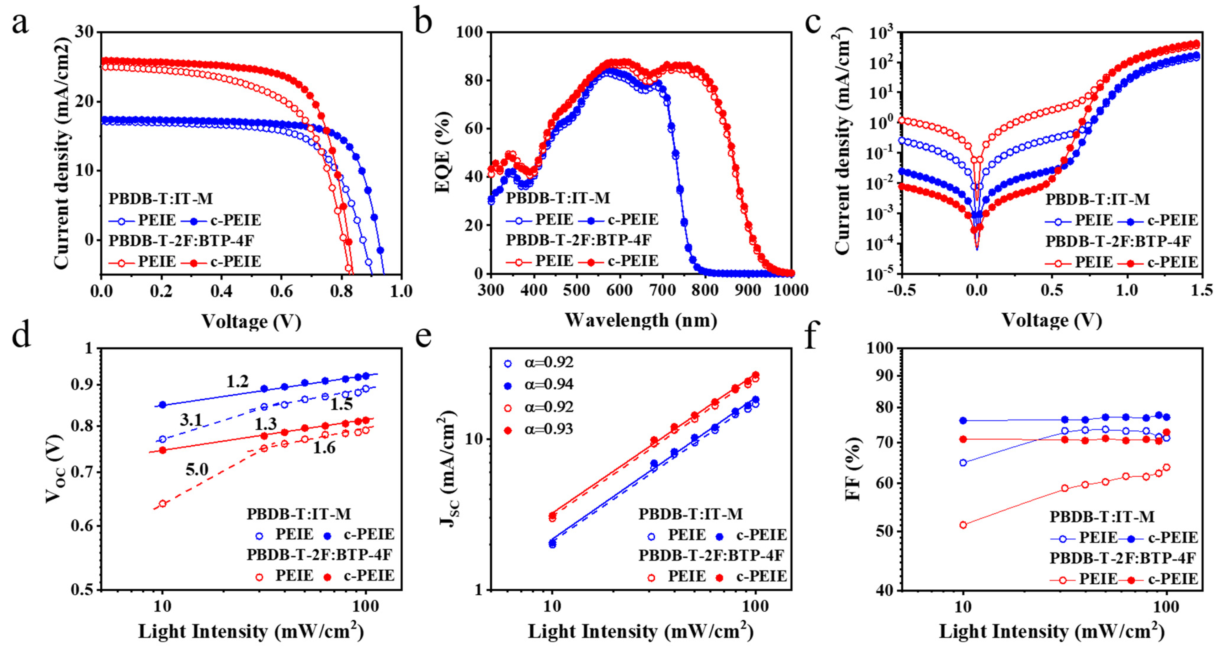
Figure 2a illustrates the current density–voltage (J-V) characteristics of inverted OPV devices with PBDB-T: IT-M and PBDB-T-2F: BTP-4F photoactive layers utilizing PEIE and Co-PEIE CILs under standard 1 sun illumination conditions, while the summary of key device parameters is presented in
Table 1. The maximum PCE of PBDB-T: IT-M and PBDB-T-2F: BTP-4F photoactive layer-based OPV with pure PEIE is 10.46% (V
OC: 0.87 V, J
SC: 17.11 mA/cm
2, and FF: 70.19%) and 12.86% (V
OC: 0.80 V, J
SC: 25.03 mA/cm
2, and FF: 63.72%), respectively, under standard 1 sun illumination conditions. Conversely, by utilizing Co-PEIE as a CIL, the PCE increases to 12.47% (V
OC: 0.92 V, J
SC: 17.42 mA/cm
2, and FF: 77.53%) and 15.51% (V
OC: 0.82 V, J
SC: 25.87 mA/cm
2, and FF: 72.77%) for PBDB-T: IT-M and PBDB-T-2F: BTP-4F photoactive layer-based OPVs, respectively. Significant improvement in V
OC and FF of Co-PEIE CIL-based photovoltaic devices could be the result of better charge transport and lower charge carrier recombination as compared to PEIE CIL-based OPV devices. In addition,
Figure 2b exhibits that the external quantum efficiencies of the Co-PEIE CIL-based photovoltaic devices are slightly higher than those of the PEIE-based devices for both PBDB-T: IT-M and PBDB-T-2F: BTP-4F photoactive layers throughout the visible region, resulting in relatively higher J
SC. Meanwhile, there was no significant difference in optical transmittance between PEIE and Co-PEIE CIL (
Figure S2). Therefore, the improved EQE values of the Co-PEIE-based devices compared to PEIE can be the result of a more efficient charge extraction.
We conducted a comprehensive analysis of the relationship between light intensity and key parameters, such as V
OC and J
SC, to gain insights into charge recombination mechanisms. We focused on trap-assisted recombination and bimolecular recombination, as well as the role of the shunt resistor. By analyzing the slope of the V
OC versus light intensity at kT/q (where k: Boltzmann constant, T: absolute temperature, and q: elementary charge), we can determine the dominant recombination mechanism. If the slope corresponds to 1.0 kT/q, it indicates that bimolecular recombination is the primary process. Alternatively, if the slope is 2.0 kT/q, it suggests that trap-assisted recombination is more significant [
32,
33].
Figure 2d represents the V
OC verses light intensity graph of PBDB-T: IT-M and PBDB-T-2F: BTP-4F active layer-based photovoltaic devices with PEIE and Co-PEIE CILs. The PEIE CIL-based OPV device with the PBDB-T: IT-M and PBDB-T-2F: BTP-4F photoactive layers shows a slope of 1.5 kT/q and 1.6 kT/q, respectively, over 0.3 sun (30 mW/cm
2) illumination intensity, whereas under lower-intensity light illuminations, the slope dramatically increases to 3.1 kT/q and 5.0 kT/q, signifying the trap-assisted recombination domination. The observed phenomenon can be attributed to the relatively high leakage current exhibited by photovoltaic devices incorporating PEIE CIL under low-light illuminations, coupled with a low shunt resistance [
32]. In the meantime, Co-PEIE CIL-based devices exhibit a slope of 1.25 kT/q and 1.27 kT/q for PBDB-T: IT-M and PBDB-T-2F: BTP-4F, respectively, which suggests that the Co-PEIE CIL-based devices exhibit reduced reliance on the light intensity, leading to a suppression of trap-assisted recombination. Moreover, the V
OC is a highly sensitive parameter in photovoltaic devices, particularly to surface recombination occurring between the BHJ layer and CIL interface. Voc of the device drop significantly as trap density increases due to surface recombination. Even though, the slope of the intensity-dependent V
OC does not reach 2.0 kT/q. Therefore, the higher kT/q slope of the PEIE-based OPV devices is likely to be the result of low R
sh, as shown in
Figure 2c. To determine the shunt resistance of the best-performing devices, we employed a double-diode fitting of the dark J-V curves, following the methodology anticipated by Suckow et al. [
34]. The calculated shunt resistance of PEIE and Co-PEIE interlayer-based OPV devices with the PBDB-T: IT-M photoactive layer was estimated as 1.59 × 10
4 Ω cm
2 and 1.36 × 10
5 Ω cm
2 from dark J-V characteristics, respectively, whereas the shunt resistance values of 6.14 × 10
3 Ω cm
2 and 3.9 × 10
5 Ω cm
2 were calculated for PEIE and Co-PEIE-based OPV devices with the PBDB-T-2F: BTP-4F photoactive layer, respectively. Under low-light conditions, the proportion of total current flowing through the shunt resistance increases, resulting in higher fractional power loss and a decrease in both V
OC and FF. Additionally,
Figure 2e exhibits the investigation of bimolecular recombination in PEIE and Co-PEIE-based OPV devices with PBDB-T: IT-M and PBDB-T-2F: BTP-4F active layers. The deviation of the slope from unity in the power law (J
SC ∝ I
α) dependence of J
SC on light intensity suggests a bimolecular recombination process [
35,
36]. Slopes calculated for PEIE and Co-PEIE CIL-based photovoltaics are 0.92 and 0.94 with the PBDB-T: IT-M photoactive layer, whereas they are 0.92 and 0.93 with the PBDB-T-2F: BTP-4F absorber layer. These results suggest that Co-PEIE CIL-based devices exhibit a relatively low bimolecular recombination, generating higher J
SC and FF under low-light illumination conditions. Moreover,
Figure 2f illustrates that the photovoltaic devices utilizing Co-PEIE CIL maintain a constant FF at relatively lower light intensities, while PEIE CIL-based photovoltaic devices experience a significant decrease in FF, indicating severe trap-assisted recombination [
37,
38].
Furthermore, to evaluate the potential role of CILs to reduce the open-circuit voltage and fill factor losses under very low light illuminations, we characterized both PEIE and Co-PEIE CIL-based photovoltaic devices under various low-light illuminations (10–0.1 mW/cm
2) including 100 mW/cm
2 (1 sun) and dark conditions, as shown in
Figure 3. These results are particularly interesting, as under light intensities of 30–100 mW/cm
2, both PEIE and Co-PEIE CIL-based photovoltaic devices, regardless of photoactive layer, showed a similar trend in terms of the change in V
OC and FF, whereas this trend altered dramatically for the PEIE interlayer-based photovoltaics under 10 mW/cm
2 illuminations.
Figure 3a,b represent the normalized V
OC and FF graphs of PEIE and Co-PEIE interlayer-based photovoltaic devices with PBDB-T: IT-M and PBDB-T-2F: BTP-4F photoactive layers under illumination intensities ranging from 10 mW/cm
2 to 0.1 mW/cm
2. No significant change in J
SC due to a change in light intensity was observed for both PEIE and Co-PEIE interlayer-based photovoltaics, as it changes linearly with a change in light intensity (
Figure S3). These results establish that under low-light conditions, Co-PEIE CIL plays an important role in maintaining a higher device performance by reducing V
OC and FF losses.
Figure 3c,d and
Figure 3e,f show the J-V curves of PEIE and Co-PEIE interlayer-based photovoltaics with the PBDB-T: IT-M and PBDB-T-2F: BTP-4F active layers, respectively, measured under different light illuminations including the dark and 1 sun illumination conditions. At low-bias voltages, it is well established that the dark current is primarily governed by the leakage current, while the light current is influenced by the disparity between the photogenerated current and the leakage current [
39,
40,
41]. In comparison to Co-PEIE interlayer-based devices, the photovoltaic devices employing PEIE cathode interfacial layer showed significantly higher dark current density and relatively lower shunt resistance. Because photogenerated current densities are enormously low under low-light illuminations, the leakage current exerts a greater influence on the total current of the devices, thus reducing both open-circuit voltage and fill factor. The relationship between V
OC and leakage current can be illustrated by the following equation [
1]:
where
n is the ideality factor,
k is the Boltzmann constant,
T is temperature, J
ph is the photocurrent, J
ds is the reverse dark saturation current, and R
sh is the shunt resistance. It is clear from the above equation that a high J
ds results in a reduced Voc. Therefore, the V
OC losses can be reduced effectively by suppressing the dark current. Consistently with previous observations, our findings also support the conclusion that achieving outstanding photovoltaic device performance under low illumination necessitates a very low leakage current and a high shunt resistance. These characteristics are crucial in minimizing power losses and optimizing the efficiency of photovoltaic devices operating in low-light conditions [
41,
42,
43,
44].
Furthermore, the exceptional hole-blocking properties of Co-PEIE interlayer-based photovoltaic devices under low light highlight their remarkable characteristics, including very low leakage current and high shunt resistance. These attributes indicate the effective prevention of undesired hole transport and leakage pathways, thereby minimizing recombination losses and enhancing the overall device performance. In contrast, the relatively poor hole blocking ability observed in PEIE CIL-based devices may be attributed to factors such as the surface roughness of the PEIE CIL, inadequate electron extraction, and increased carrier recombination at the interface between the BHJ layer and the CIL. These limitations in PEIE CIL contribute to a compromised device performance, particularly in low-light conditions. To investigate the role of surface roughness of CIL influencing the leakage current and shunt resistance, we analyzed surface roughness of PEIE and Co-PEIE interlayers by utilizing an atomic force microscope (AFM). The topographic AFM images of the PEIE and Co-PEIE interlayers are shown in
Figure S4. Both the PEIE and Co-PEIE interlayers showed comparable surface roughness, which negates the major cause of a high leakage current and low shunt resistance of PEIE interlayer-based OPV under low-light illuminations. We also analyzed electron extraction of PEIE and Co-PEIE interlayers under different light illumination intensities such as 100, 1 and 0.1 mW/cm
2. To evaluate the electron extraction of PEIE and Co-PEIE interlayer-based photovoltaics with PBDB-T: IT-M and PBDB-T-2F: BTP-4F active layers, the photo-current densities (J
ph) were measured as a function of the effective applied voltage (V
eff) under different illuminations conditions and plotted on double-logarithmic scale, as shown in
Figure 4. The J
ph represents the difference in current densities between different light intensities and dark. The V
eff can be evaluated from the difference in voltage (V
eff = V
0 − V
app), where V
0 is the voltage when J
ph = 0, and V
app is the applied voltage. When the effective applied voltage rises, all of the charge carriers in the photo-absorber layer may be swept out, resulting in a saturated photocurrent. As can be seen in
Figure 4a,b, under 100 mW/cm
2 (1 sun) illumination conditions when the effective applied voltage is around 0.2 V, the J
ph of both PEIE and Co-PEIE interlayer-based photovoltaic devices can reach a saturated current, whereas under low-light intensities (1 and 0.1 mW/cm
2), only Co-PEIE CIL-based OPV devices can reach saturation at a lower effective applied voltage. These results illustrate that the Co-PEIE interlayer has a better charge extraction capacity under low-light illuminations compared to PEIE. Furthermore, the charge extraction was evaluated using time-resolved photoluminescence (TRPL) decay characterization with excitation at 405 nm and emission at 850 nm for the BTP-4F acceptor material deposited on PEIE and Co-PEIE interlayers, as shown in
Figure S5. The TRPL spectrum of the PEIE and Co-PEIE interlayers with BTP-4F exhibits a decay time of 1.08 ns and 0.97 ns, respectively. The Co-PEIE interlayer has a shorter decay time, indicating that electron extraction at the Co-PEIE/active layer interface is much efficient compared to PEIE/active layer interface. Comparatively reduced charge extraction property of PEIE CIL-based devices could be the result of poor electron mobility and relatively higher charge carrier recombination at the BHJ/CIL interface. In our previous report, we extensively discussed how the utilization of a pure PEIE interlayer in photovoltaic devices could lead to a decrease in electron mobility due to the undesired reaction between PEIE and NFAs. This reaction, in turn, results in an imperfect molecular structure of the NFAs, leading to reduced charge transport capabilities [
24,
25]. On the other hand, when Co-PEIE is employed as a CIL, it offers a notable enhancement in electron mobility. This improvement stems from the effective prevention of the undesired reaction between PEIE and NFAs, thereby leading to enhanced charge carrier transport and reduced interfacial resistance at both the BHJ/CIL and CIL/electrode interfaces. Consequently, we believe that the serious trap-assisted recombination in PEIE CIL-based OPV devices possibly originates at the BHJ/CIL or CIL/electrode interface, as pure PEIE CIL cannot effectively block the hole, resulting in electron–hole recombination [
1,
40].
Finally, to evaluate the device performance of PEIE and Co-PEIE CIL-based photovoltaics under indoor illumination, we utilized a 2700 K LED lamp. Accurate measurements of the photovoltaic device’s PCEs under low-light conditions are of great interest. Therefore, the lamp power must be measured with a high-precision power meter. We precisely measured the emission power spectra of LED lamps at 200, 500, 1000 and 2000 lux to accurately assess LED lamps to simulate indoor lighting environment.
Figure 5a depicts the emission power spectra and integrated power densities of the LED lamp at various light intensities. The integrated power densities calculated from LED lamp emission spectra at 200, 500, 1000 and 2000 lux are 56.14, 137.95, 277.21 and 556.13 µW/cm
2, respectively. The theoretical current densities were evaluated by combining the photon flux spectra with their corresponding illumination intensities, as illustrated in
Figure 5b, and theoretical current densities for LED lamps at approximately 200, 500, 1000 and 2000 lux intensities were calculated as 26.45, 65.01, 130.70 and 261.99 µA/cm
2, respectively.
Figure 5c,d illustrate the J-V characteristics of PBDB-T: IT-M and PBDB-T-2F: BTP-4F active layer-based OPV devices with PEIE and Co-PEIE CILs at 200, 500, 1000 and 2000 lux under the LED (2700 K) lamp. The detailed IOPV device parameters of both PBDB-T: IT-M and PBDB-T-2F: BTP-4F active layer-based IOPV devices with PEIE and Co-PEIE CILs at different light intensities are presented in
Table 2. The J
SC and V
OC of IOPV devices increase significantly as the light intensity increases from 200 to 2000 lux, due to an increase in the number of incident photons. Since incident light power directly relates to J
SC, the slope of J
SC versus incident light intensity under LED lamp source in our IOPV device is 0.99, which implies that the photons-to-electron conversion ratio remains almost constant as incident light intensities decrease. The best PCEs measured for PBDB-T: IT-M active layer-based IOPV devices under the LED light source at 200, 500, 1000 and 2000 lux illuminations are 9.65, 17.53, 18.31 and 19.20% for PEIE CIL and 19.53, 21.58, 22.60 and 23.66% for Co-PEIE CIL, respectively. The poor device performance of PEIE CIL-based IOPV devices under low-light illuminations is the result of a significantly high leakage current and low R
sh that directly affect the V
OC and FF of IOPV devices, as shown in
Table 2, whereas the best PCEs measured for PBDB-T-2F: BTP-4F active layer-based IOPV devices under LED light source at 200, 500, 1000 and 2000 lux illuminations are 4.90, 8.98, 14.32 and 14.74% for PEIE CIL and 14.84, 17.02, 18.34 and 19.61% for Co-PEIE CIL, respectively. In addition, with regard to the role of CILs, the poor IOPV device performance of PBDB-T-2F: BTP-4F-based devices compared to PBDB-T: IT-M-based devices is due to the spectral mis-match of PBDB-T-2F: BTP-4F absorbance and LED light source emission spectra. In this study, we used PBDB-T-2F wide-bandgap polymer donor and BTP-4F low-bandgap acceptor materials, which can effectively convert solar photons to electrons under standard 1 sun illumination conditions. In contrast, in an indoor environment, absorbance spectra above 750 nm are redundant, resulting in significant photovoltage [
10]. These losses can be recovered to some extent through fine tuning the CILs energy levels, which can effectively reduce the trap-mediated charge recombination under very low-light illuminations resulting in reduced V
OC and FF losses. The same trend can be observed in PBDB-T-2F: BTP-4F-based IOPV devices with Co-PEIE CIL as compared to PEIE CIL. We observed that the V
OC loss of PBDB-T: IT-M and PBDB-T-2F: BTP-4F-based devices with PEIE CILs under low-light illuminations (1000 lux) as compared to 1 sun illumination conditions is around 25% and 24%, respectively, whereas these losses reduce to 17% and 21% for PBDB-T: IT-M and PBDB-T-2F: BTP-4F-based devices with Co-PEIE CILs, respectively. Normalized V
OC and FF of both PBDB-T: IT-M and PBDB-T-2F: BTP-4F-based IOPV devices with PEIE and Co-PEIE CILs under 200–2000 lux light illuminations are presented in
Figure 5e,f. Our findings show that incorporating metal salt ions improved the electronic energy level of PEIE, resulting in reduced V
OC and FF losses.


