
Nanoimprinting of Biomimetic Nanostructures


Profactor GmbH, Im Stadtgut D1, 4407 Steyr-Gleink, Austria
Nanomanufacturing 2022, 2(1), 17-40; https://doi.org/10.3390/nanomanufacturing2010002
Submission received: 22 December 2021
/
Revised: 21 January 2022
/
Accepted: 26 January 2022
/
Published: 9 February 2022
Abstract
:Biomimetic micro- and nano- structures have attracted considerable interest over the last decades for various applications ranging from optics to life sciences. The complex nature of the structures, however, presents significant challenges for fabrication and their application in real-life settings. Nanoimprint lithography could provide an interesting opportunity in this respect. This article seeks to provide an overview of what has already been achieved using nanoscale replication technologies in the field of biomimetics and will aim to highlight opportunities and challenges for nanoimprinting in this respect in order to inspire new research.
1. Introduction
1.1. Nanoimprinting
Nanoimprint lithography [1,2,3] is a method to replicate micro- and nanostructures. Since its beginnings in the 1990s [4,5,6] it has seen a strong increase in popularity and use both in academia and industry.
In a typical nanoimprint process as sketched in Figure 1, a nanopatterned stamp is brought into contact with a substrate that is coated with a liquid polymer. As soon as the stamp is in good contact with the substrate and the polymer has filled all the cavities of the stamp, the polymer is hardened. This can be achieved typically either by UV-curing (for UV-curable polymers), which is then called UV-NIL, or by cooling down below the glass transition temperature (for thermoplastic materials), which is then called hot embossing. As soon as the imprint material is hardened, the stamp can be removed and the nanopattern has been copied. The hardened polymer can now be used further in a semiconductor-type of process to transfer the pattern into the substrate, e.g., by reactive ion etching, or the polymer already represents the final structure, e.g., a diffractive optical element.
The stamp that is used in such a nanoimprint process is typically a negative copy of a master structure. This is done to keep the master safe and limit the number of replication processes with the master directly. Assuming that with a single stamp 100 imprints can be made and 100 stamps can be replicated from the master, in total 10,000 imprints can be made from a single master. In many cases the stamp can be used many times before it needs replacement [7,8].
Nanoimprint lithography combines several features which make it very interesting for numerous applications. In the following sections these characteristics are briefly discussed and exemplary references are given.
1.1.1. High Resolution
1.1.2. Direct Patterning of Complex and Hierarchical Structures
Nanoimprinting is able to perform single-step patterning of multilevel or hierarchical patterns or patterns with very different dimensions. If the right stamp (and master) is available it is possible to fabricate in a single imprinting step structures of very different lateral dimensions [14,15], of different vertical dimensions with multiple height levels [16,17,18], or curved surfaces [19] and hierarchical structures [14,20,21,22]. It is also possible to perform nanoimprinting on complex curved objects [23,24,25,26]. Figure 2 shows an example for a pattern that combines features on different length scales which can be fabricated using nanoimprinting in a single step. To fabricate the master structure, first the pattern with the larger length scale was replicated using NIL, then—on top of this pattern—the short periodicity grating pattern was nanoimprinted. This pattern was then used as a master for stamp fabrication to be able to imprint the complex pattern in one single imprinting step. Details can be found in reference [14].
1.1.3. Direct Patterning of Functional Materials
While for conventional optical lithography typically a pattern transfer is necessary, in nanoimprinting a functional material can be patterned directly, thus reducing the number of process steps significantly (e.g., [27,28,29]). Such functional materials can serve optical properties (such as for diffractive optical elements) [30,31,32,33,34] or can directly act as microfluidic channels [35,36,37,38,39] or substrates for further processing [40,41], where the nanoimprinted material remains a functional component of the final device. Also, organic semiconductors have directly been imprinted [42], sol-gel materials [7,43], even silicon [44] or metals and ceramics [45].
1.1.4. Cost-Effective Large-Area Patterning
Nanoimprinting is possible on wafer scale [16] even on display sized panels [46,47,48,49] and in large area roller-based processes [50,51,52,53,54,55,56]. Figure 3 shows a photograph of the roll-to-plate UV-nanoimprint (R2P UV-NIL) tool at PROFACTOR. Cost-effectiveness and suitability for production of nanoimprinting has been addressed in many publications, e.g., [57,58,59,60,61].
1.1.5. Different Types of Nanoimprinting
To avoid misunderstandings, a short clarification regarding the term “nanoimprinting” and explanations of which types of nanoimprinting will be dealt with in this article should be given here. As already briefly mentioned in the beginning, the focus will be on nanoimprinting methods where material on the surface of a substrate is displaced and shaped into the desired topography. This includes the following variants:
UV-NIL–UV-based or UV-curing nanoimprinting, using a material that is hardened by UV-radiation. (e.g., SmartNIL® [46], J-FIL [62], SCIL [63], STU® simultaneous thermal and UV [64]);
T-NIL–thermal NIL, using a material that can be thermally cured (e.g., SCIL [63]), sometimes also called thermally curing NIL;
HE-Hot embossing, using a thermoplastic material [5]. It should be noted here that nanoimprinting using thermoplastic materials is sometimes also called thermal NIL in literature. The reader should be aware of this possible mixup between thermal and thermally curing NIL;
Reversal NIL—all of the aforementioned variants can in principle also be performed in a reversal way, meaning that the stamp is coated instead of the substrate [65].
This article will not cover molecular imprinting and micro contact printing. Micro contact printing (µCP) [66,67,68] or nano contact printing (nCP) is a method to deposit for example thin layers or monolayers of biomolecules on surfaces. Also, here the technical challenges and the solutions applied are often similar between nanoimprinting and µCP (e.g., large-area homogeneous contact between stamp and substrate), but the final result is rather different, e.g., a glass surface with a regular protein pattern.
This article will, therefore, focus on nanoimprinting methods that mechanically modify a polymer surface to generate a biomimetic topographical pattern. The polymer might have some specific chemical properties, which are however typically not modified during the nanoimprinting process.
For many examples mentioned in this paper, casting processes have also been used to replicate the biomimetic features. In contrast to pure casting processes, nanoimprinting aims at creating the final pattern in a thin film on top of a substrate. So, in general a casting process would not be considered to be a nanoimprint process (although casting is often used to fabricate PDMS (polydimethylsiloxane) stamps from nanostructured master structures). Not only, but especially, in the context of biomimetics very interesting results have also been obtained by replica casting. Therefore, these will also be referred to in this paper.
1.2. Biomimetics
Biomimetics is the use of solutions nature has found in the course of evolution to all kinds of challenges in engineering sciences. Studying how nature addresses different problems starting from mechanical challenges in tree branches and bones of animals to creating colours on butterfly wings can give insights into problem-solving strategies, that are typically resource efficient and have been optimized for millions of years. Many examples will be mentioned below, but the list is not exhaustive. There many excellent reviews dealing with biomimetics and the reader is referred to them for further reading, e.g., [69,70,71,72].
The use of biomimetics for sensors is discussed in, e.g., [73]. Material design for composite materials [74] or antifouling materials [75] has been discussed as well as its use in additive manufacturing [76]. Many other examples could be mentioned here. This paper will also only focus on surface effects that are accessible using nanoimprint lithography.
2. Nanoimprinting and Biomimetics
Suitability of Nanoimprinting
Due to the often complex nature of the structures designed by nature, nanoimprinting is a technology well suited to the replication of such structures. If there is a master available, in general you can readily replicate the nanostructures. The challenge of master fabrication will be discussed in the next paragraph. The fact that you can—in a single processing step—replicate complex hierarchical structures using nanoimprinting is especially helpful in the context of biomimetic structures. The interest in nanoimprinting in combination with biomimetics has been growing steadily over the last few years, which is illustrated in Figure 4, which plots the number of publications found when searching for “nanoimprint biomimetics” on Google scholar [77] per year.
3. Functionalities
In this section, nanoimprint results to achieve different functionalities based on biomimetic structures will be presented. The results will not be discussed in detail, which is undertaken in the respective papers, but an overview will be given on what kind of structures have been realized using nanoimprinting. This overview can only try to mention many interesting papers, but cannot be complete in any sense. The order in which the topics and individual papers are presented does not imply ranking in any sense. A review of biomimetic structures for functional applications is given in, e.g., [78].
3.1. Optics
Many applications of nanoimprint processes in research and industry belong to the field of optics. Here, the combination of directly patterning a functional material and creating a complex shape in one single patterning step often plays an important role and is therefore well suited for nanoimprinting.
3.1.1. Structural Colors
Structural colors are colors that are not based on pigments but on nanostructured materials [79,80,81,82]. They can be found in insects [83,84] like butterflies [85,86,87] and beetles, spiders [88,89], birds [86,90,91] and fish [92]. Constructive and destructive interference, diffraction and randomness come together to achieve a unique color impression.
Figure 5 (left) shows a cross section of a nanoscale element that can be found on the wings of the Morpho butterfly. It is elongated in the y-direction together with other such elements responsible for the metallic blue appearance of the butterfly. Saito et al. have been working intensively on structural colors [82], and especially also on the Morpho butterfly. The blue color of this insect’s wings has drawn a lot of attention. The mechanisms behind the color generation are discussed in [93]. In [94,95] they describe how depositing a multilayer stack on a substrate that has been prepatterned using nanoimprinting can mimic the color of the butterfly. Such structures can even be transformed into pigments and added to a lacquer, e.g., for automotive applications [96].
Also the multilevel undercut nanostructures have been directly replicated using nanoimprinting [97], see Figure 6. The authors could demonstrate that it is possible to replicate a nanoimprint stamp from an undercut master and to use those stamps in a UV-based nanoimprinting process again. The crucial enabling factor to allow for successful nanoimprinting of such structures is finding the right material with suited mechanical properties. The mastering was done using optical or e-beam lithography and reactive ion etching on a substrate containing a multilayer stack of Si/SiO2 to provide the material contrast for selective etching [98].
Zobl et al. [99] could show that it is also possible to directly use the butterfly wing as the original structure and to create a stamp and a positive epoxy cast from such a structure showing all the biological details of the wing. Also, Huang et al. [100] used natural butterfly structures for creating a biomimetic replica, but employed a process that destroys the natural master structure.
3.1.2. Antireflection Structures
The nanostructures found on the eyes of certain insects especially on moths have a distinct antireflection effect. The structures were reported in the 1960s [103,104] and the optical properties have been investigated (e.g., [105]). Today moth-eye inspired structures are commercially used for different applications (e.g., [106,107,108,109]). An array of conically shaped structures (see Figure 7) with a periodicity of around 200 nm a height of 200 nm creates a layer with an effective graded refractive index greatly reducing the reflectivity of the surface [110]. It is suspected that the reduction of reflections on the insects’ eyes hides them from predators at night and additionally improves night vision [110].
Nanoimprinting of such structures has been reported on various substrates often with the motivation of increasing the performance of photovoltaic cells or for display applications.
Broadband moth-eye antireflection coatings fabricated by low-cost nanoimprinting have been reported in [111]. Waver scale soft roller-based UV-NIL was utilized in this publication. Roll-to-plate UV-NIL with a nickel mold was also used in [112] to fabricate moth eye structures on polycarbonate (PC) substrates. For flexible display applications also the mechanical stability of the nanostructures is important. Tan et al. [113] used a UV-curable hardcoat material to prepare moth-eye structures on a flexible polyethylene terephthalate (PET) and triacetyl cellulose (TAC) substrates. Polymer templates, which were obtained from nickel masters in a hot-embossing process, were used in [114] to fabricate moth-eye antireflective structures on glass substrate in a UV-NIL process. R2R UV-NIL was used by Burghoorn et al. in [115] to create moth-eye structures in OrmoComp® on foils. Hot embossing was used in [116] to prepare antireflection structures in PMMA.
In contrast to the papers mentioned so far, where a functional coating was nanostructured using nanoimprinting, Boden and Bagnall [117] used hot-embossing nanoimprinting, lift-off and subsequent etching to transfer the moth-eye pattern into a silicon.
In [118] anodized aluminum oxide (AAO) membranes were directly used as stamps with HSQ as imprint material on glass. The AAO stamps were etched away after imprinting. An AAO mold was also used in [119] by Zhang et al. in a R2R UV-NIL process to fabricate moth-eye structures on PET substrates. An etched glassy carbon layer was used as a stamp in a UV-NIL process by Yano et al., in [120].
Moth-eye structures on curved surfaces were reported in [23]. Here the possibility to nanoimprint on curved objects was used to directly imprint moth-eye structures on lenses. Figure 8 shows an example of such a process, where the substrate was a full hemisphere. Biomimetic antireflective structures have also been fabricated on microlens arrays [121]. Xie et al. [33] present a single step UV-NIL process, which replicates microlenses including moth-eye structures.
Although not strictly spoken a nanoimprint process also the paper of Schulte et al. [122] has to be mentioned here. It presents a replication technique based on [123] and reflection measurement results of different plant surfaces. Complex surface structures of plants such as Ficus elastica, Chrysanthemum leucanthemum or Tulipa gesneriana were replicated.
The following table briefly summarizes the main features of the processes reported in the aforementioned publications. As can be seen, many approaches lead to interesting results, which shows that the flexibility of nanoimprinting is an important aspect for potential applications.
Table 1 gives an overview of functionalities inspired by natural sources also indicating the type of nanoimprint process used. In this table and also in the following tables the features are indicated as “artificial” or “natural”. “Natural” means that the master was directly taken from nature, e.g., a rose petal, while “artificial” micro-/nano features are fabricated in a lab using some micro-/or nanostructuring technology like electron beam lithography. A brief overview of these mastering technologies is given in Section 3.6.
3.2. Surface Interactions with Solids
The surface structure and chemistry of any object or animal plays a crucial role in its interaction with the environment. This can be related to the movement of the animal, to its interaction with water or to its defense against bacteria. Some of the solutions nature has provided in this respect will be mentioned here.
3.2.1. Friction
The skin of certain snakes exhibits interesting friction properties, a frictional anisotropy based on micro-nanostructures [124]. Figure 9 shows an image of the skin of the California King Snake (Lampropeltis getula californiae) [124,125]. The structures exhibit a pronounced anisotropy, which is also reflected in the friction properties.
In [126] the authors describe a process where a foil patterned using UV-NIL is used as an inlay for ceramic injection molding to obtain snake-skin inspired structures on a ceramic surface. The respective grey-scale e-beam mastering process is explained in [127]. It could be shown that the desired friction modification could be achieved on a ceramic surface. Figure 10 shows an AFM image of the ceramic surface.
Also, polymeric surfaces have been investigated. Snake skin-inspired surfaces fabricated by a moulding technique [128] have been shown to exhibit interesting and anisotropic friction properties in, e.g., [124,129].
Yoon et al. [130] as well as Burton et al. [131] and Singh et al. [132,133] used hot embossing to modify polymeric surfaces and assess the friction properties. The background to their work is the study of MEMS-related tribological questions. The natural inspiration was taken from the lotus leaf, however an artifical structure was created. In their work Yoon et al. use different nanoimprint processing conditions to modify the final geometry of the pattern and investigate the influence on the friction.
3.2.2. Adhesion
The special properties of the Gecko foot have been of interest since the beginning of the 20th century [136,137] and there have been multiple attempts to mimic the behavior of Gecko feet. The working principles and properties of the Gecko-adhesion are discussed, e.g., in [138,139]. An overview of hierarchical bio-inspired adhesive surfaces is given in [140].
An approach to the development of a synthetic Gecko tape is described by Davies et al. in [141]. The authors use photolithography to fabricate a master structure and nano moulding to create the adhesive hair structures in silicon rubber creating a mushroom-shaped structure, as shown in Figure 11a. Similar structures are reported in [142]. Kwak et al. [143] demonstrate micropillars with a triangular cross-section also made from PDMS. Hot embossing combined with electrically induced polymer deformation is utilized by Hu et al. in [144] to create different geometries of mushroom-shaped structures made from PMMA (poly methylmethacrylate).
PDMS casting is also used in [145] by Wang et al., However, they also create mushrooms with a nano rough top, similar to what is shown in Figure 11b, by performing their molding process on a nanostructured substrate.
Raut et al. use a sacrificial-layer mediated hot embossing nanoimprinting method to fabricate Gecko-inspired dry adhesives [146] from polycarbonate sheets and demonstrated it in a climbing device. Their structures resemble the image in Figure 11c. In Terashima et al. [147] a structure like this is replicated using UV-NIL based on a master structure fabricated by high-resolution two-photon polymerization (2PP). Based on a porous anodic alumina (PAA) template Ho et al. [148] used a variant of hot embossing—capillary force lithography [149]—to fabricate hierarchical Gecko-structures in polycarbonate (PC).
Table 2 provides an overview of functionalities, inspiration source and NIL process used in the context of biomimetic surfaces, which influence the interaction between solids.
3.3. Surface Interaction with Liquids
For many animals and plants, it is a matter of survival to adequately handle liquids that contact their surface. Therefore, it is not surprising that many different surface structures have evolved to address different challenges, such as how to repel water to achieve self-cleaning, how to guide and harvest water in desert regions, or how to reduce drag when moving in water.
3.3.1. Repelling of Liquids
The most famous example for a self-cleaning surface is the lotus leaf [150]. However, many other plants and animals also exhibit superhydrophobic surfaces or at least surfaces with a very high contact angle of water [151,152] and applications and the fabrication of such surfaces has generated much interest [153,154,155,156,157,158,159].
Hwang et al. [160] used PDMS casting from the backside of bamboo leaves to create a stamp for UV-based NIL. They compared different fabrication procedures for the stamp to achieve an optimized imprint performance. In [43] Saison et al. also used PDMS stamps copied from natural lotus leaves and butterfly wings to create superhydrophobic surfaces in sol-gel materials. A UV-curing polyurethane acrylate (PUA) stamp material was used to obtain stamps from a natural rose petal to imprint into a UV-curable nanoimprint material by Choo et al. [161]. Yang and coworkers [162] used nanoimprinting on wood and a rose petal as master structure to create superhydrophobic wood surfaces. In [163] the authors coated the lotus leaves they used as master structures with inorganic films to directly use them as nanoimprint stamps in a hot-embossing process.
Starting from simple artificial structures, Sun at al. varied the process conditions during a hot-embossing process to obtain a broad range of different biomimetic hierarchical structures [164]. Also, preparing artificial biomimetic structures using induced wrinkling, Li et al. [165] presented a work with a focus on large-area R2R NIL fabrication of biomimetic surfaces for superhydrophobicity.
Moth-eye structures—often primarily investigated for their antireflection properties—also exhibit superhydrophobicity. Sun et al. present this aspect in their paper [112]. This is also highlighted in [166] by Kim et al. Zhang et al. [167] presented a combined UV and thermal NIL approach to fabricate antireflective and superhydrophobic sol-gel structures on glass substrates.
The combination of hot embossing and self-induced wrinkling to create superhydrophobic structures in poly (hydroxyethyl methacrylate) films is reported in [168].
The surface structures of different plant surfaces have been replicated by moulding by Koch et al., in [123] and the contact angles have been investigated.
A concept related to superhydrophobic surfaces is so-called SLIPS (slippery liquid infused porous surfaces) [169]. Nanoimprinting of such biomimetic surfaces is shown in [165]. Li et al., use roll-to-roll nanoimprinting on polyethylene terephthalate (PET) films as substrates.
Anti-fogging and anti-icing properties are often investigated in association with superhydrophobicity. In [121] this is shown by Raut et al., for the example of microlenses with moth-eye structures. They use two consecutive nanoimprint steps to achieve their goals. The fabrication of biomimetic polymer nanocone films based on a hexagonally packed alumina taper-nanopore template is shown in [170]. There, Zhang et al., demonstrate the importance of the tip geometry to achieve the desired antifogging properties.
A different approach is taken by Li et al. [171], who use nanoimprinting to create moth-eye structures on PMMA but coat them with silica nanoparticles to make the surface superhydrophilic, which also results in anti-fogging properties of the surface. Anti-icing of hot embossed FEP (fluorinated ethylene propylene) films is investigated by Durret et al., in [172].
A review of bio-inspired antifogging materials was undertaken by Han et al. in [173] for further reading.
Omniphobicity is often associated with reentrant or undercut structures. Hensel et al. [174] present biologically inspired omniphobic surfaces by reverse imprint lithography. Structures such as those sketched in Figure 12c are arranged in a regular array and interconnected with each other. The inspiration for these complex structures was taken from the structures found on the skin of springtails (Collembola) [175,176].
3.3.2. Liquid Transport
In nature there is not only the need for non-wetting surfaces, but also surfaces that direct water or other liquids in a desired direction. Lifka et al. [177] present a short overview of passive, unidirectional fluid transport and an optimized surface structure for passive, unidirectional fluid transport. Zhang et al. [178] provide a review of this interesting phenomenon of unidirectional transport of liquids induced by bioinspired micro-nanostructures.
Based on the structures found in pitcher plants [179], Peng and Wu describe a droplet array generated by roller nanoimprint in [180]. They use PDMS stamps with the biomimetic structures as microfluidic chips to entrap droplets between the stamp and the substrate. In a R2R UV-curing process they seal the chip with the polymer substrate, trapping single droplets making use of the special behavior of the liquid on the biomimetic surface.
3.3.3. Drag Reduction
The skin of sharks exhibits interesting drag-reduction properties (along with anti-biofouling and antimicrobial properties) [181,182]. Figure 13 shows SEM images of epoxy replicas [181] of real shark skin.
Pu et al. [183] also prepared direct copies from real shark skin using PDMS moulds and polyurethane. In [184] Han et al. report the use of hot embossing to replicate natural shark skin. They also prepared a large-area surface by stitching several replicated samples together for measurements of the drag reduction effect.
Roller-based UV-NIL of sharkskin structures is presented in [185] by Chen et al. In their paper they propose a UV-NIL tool, that could directly perform the patterning on the surface of ships and measure the drag reduction properties.
Comprehensive reviews on recent advances in microstructured surfaces and their applications for drag reduction are presented in [158,186].
Table 3 briefly summarizes some examples where nanoimprinting was used to achieve bio-inspired surfaces that influence the interaction with liquids.
3.4. Life Sciences
An interesting area of applications for nanoimprinting are the life sciences, where NIL is used for the fabrication of microfluidic devices (e.g., [187] or [188]) as well as substrates for cell growth. For the latter in particular, biomimetic structures are used and will be discussed in Section 3.4.1. Another application where biomimetic structures are often used are antimicrobial or anti-biofouling surfaces. Examples for nanoimprinting of such structures are given in Section 3.4.2 below.
3.4.1. Cell Growth
In contrast to all surfaces mentioned so far, the micro-/nanostructures relevant for cell growth are typically not easily accessible, since they cannot be found on the outer surface of animals or plants. The micro-nanostructured surfaces employed for cell growth, therefore, are in many cases artificial and the research is aimed at understanding how different substrate micro-/nanotopographies influence the growth, proliferation or differentiation of different cells. The structures investigated in this field of research are not biomimetic in the sense that, e.g., the structure found on the moth-eyes is used for antireflective coatings on solar panels, but biomimetic as they try to mimic the natural biological environment of the cells, or at least some aspects of it, to better understand the cells. This is a very large field of research, just considering the large number of different organs and cells of interest in the human body [189,190], which potentially exhibit different behavior on the same surface. There are numerous reviews available dealing with how micro- and nanostructures influence cell behavior (e.g., [191,192]) and only selected nanoimprint related examples can be mentioned here briefly.
For the control of cell-growth, chemical patterning of surfaces is interesting (see, e.g., [193,194]), which falls into the domain of nCP or µCP, which will not be covered here.
Using hot embossing it is possible to directly pattern standard substrates like tissue culture polystyrene. This has been demonstrated by Hu et al. [195] and the influence of the imprinted structures on the growth of bovine pulmonary artery smooth muscle cells was investigated. High aspect ratio pillar arrays with an aspect ratio of up to 5 were hot embossed in polycarbonate by Viela et al. [196]. They tested C17.2 cells (mouse multipotent neural progenitor or stem-like cells) and found that different patterns triggered very different responses. In another paper dealing with stem cells, Wu et al. [197] used hot embossing of polycaprolactone (PCL) to prepare their substrates for cell growth. Also in this work, differences in nanotopography led to changes in morphology and cytoskeletal structure, which in turn influenced cell aggregation and cell differentiation.
Double-sided nanoimprinting is presented in [198] by Seunarina et al. for the hot-embossing fabrication of 3D polymer scaffolds for tissue engineering.
Randomly organized nanostructures mimicking the irregular distribution of natural collagen fibers were replicated by hot embossing and transferred into gold structures in [199] to improve growth of neurons. PCL membranes were used as substrates for cell growth by Monteiro et al. [200]. The stamp is copied from a natural leaf (Rubus fruticosus, a blackberry species) and exhibits complex hierarchical structures.
An especially interesting application is the surface structuring of implants to improve the biocompatibility, bone ingrowth etc. Titanium is a material that is often used for implants [201,202]. In [203] Domanski et al. present results of a cytotoxicity study of cells on nanopatterned titanium surfaces. Nanostructuring was achieved by hot embossing and subsequent reactive ion etching into the substrate. Although the results presented were obtained on flat titanium, nanoimprinting is capable of patterning on curved surfaces (e.g., [26]).
Direct imprinting of titanium using ultra-nanocrystalline diamond stamps is presented by Greer et al. [204]. They used an anodization step to lower the required imprint force and can use a roller-type of imprinting process to pattern a titanium rod.
3.4.2. Antimicrobial and Anti-Biofouling Surfaces
Somehow the opposite of providing a hospitable environment for cells is establishing an antimicrobial surface, aiming at killing bacteria, inactivating viruses, making it unattractive for cells to reside on a surface.
Surfaces to achieve this have been artificially engineered (e.g., [205]) but more direct biomimetic approaches have also been followed (e.g., [206]). In this context, the needle-like structures on cicada or dragonfly wings in particular have attracted considerable interest, but also the moth-eye structure and the skin of sharks. An overview of different approaches is given in [207].
In [208] Zhang et al., used natural cicada wings as nanoimprint stamps for hot embossing. Reid et al. [209] used UV-curing PEG to copy the structures of natural cicada wings two times to obtain the positive structure in the end again. They found the antimicrobial effect also in the PEG replicas.
Antibacterial effects of the artificial surface of nanoimprinted moth-eye film were investigated by Minoura et al. [210]. They find that moth-eye surfaces fabricated using UV-NIL in UV-curable PEG exhibit significant antibacterial effects when tested with Staphylococcus aureus and Esherichia coli. Similar findings also on UV-NIL fabricated moth-eye films are reported in [211]. Low adhesion of E. coli was also observed on SLIPS surfaces fabricated by nanoimprinting [165].
Pu et al. [183] present anti-biofouling results on copies of real shark skin with respect to the adhesion of algae. Bioinspired photocatalytic shark-skin surfaces with antibacterial and antifouling properties are reported in [212] by Arisoy et al. They used UV or IR curing nanoimprinting of a nanoimprint material that contains titanium dioxide (TiO2) nanoparticles. The formation of Staphylococcus aureus biofilms on shark-skin inspired PDMS surfaces was investigated in [213]. The shark-skin inspired surface significantly reduced biofilm formation. In [214] May et al. showed the effectiveness of shark skin-inspired PDMS patterns in reducing the biofilm formation on endotracheal tubes. Using real shark-skin as master structure for a UV-NIL process is reported in [185]. Chen et al. tested the surfaces for their anti-fouling performance and found that the biomimetic shark-skin surface exhibits very good properties in this respect.
Table 4 gives an overview of some exemplary publications in which nanoimprinting was used to fabricate biomimetic surfaces for life sciences applications.
3.5. Energy Applications
The application of biomimetic structures for energy applications should be mentioned here separately, although the basic effects have already been discussed before, since addressing the challenges of the climate crisis is of high importance. Providing clean renewable energy is one of the important challenges of coming years [215,216,217].
Nosonovsky and Bhushan [218] provide an overview of the multiscale effect relevant on biomimetic surfaces and how they could be used for energy conversion and green engineering.
The efficient light management and self-cleaning properties of natural surfaces such as those of the rose petal are interesting for photovoltaic applications. Fritz et al. [219] not only investigate the replication process from natural rose petals but also address the important aspect of upscaling. They use hot embossing and stitching to create larger area rose petal structures and investigate the performance of CIGS (copper indium gallium diselenide) photovoltaic cells equipped with such foils.
Deniz et al. [118] prepared moth-eye inspired sol-gel layers for anti-reflective applications in photovoltaics. AAO membranes were used as stamps directly. PDMS stamps and PMMA as imprint material were used in [220] by Chen et al., The aim in this work was also the fabrication of anti-reflective surfaces for photovoltaics. The benefits of biomimetic light harvesting and anti-reflection and self-cleaning are also relevant for organic photovoltaics as demonstrated by Chen et al. [221]. Moth-eye nanostructures were directly nanoimprinted into functional layers of the photovoltaic device.
The lotus leaf effect is utilized to prepare a robust triboelectric nanogenerator (TENG) by Choi et al. [222]. The lotus leaf TENG performs better than the flat reference TENG. Furthermore, the superior self-cleaning capability is relevant for the application.
In [223], Back et al., fabricated periodic nanostructures from high-temperature stable sol–gel material using UV-based nanoimprinting for light management in solar cells.
Table 5 briefly summarizes the processes and functionalities mentioned in this section.
3.6. Mastering of Biomimetic Structures
In general, mastering is a critical step for nanoimprinting. The replicated structure cannot be better than the original structure. For biomimetic structures there are two approaches: you can try to replicate the nanostructure directly from what you find in nature or you can try to artificially recreate the structures. In the tables above, it has already been pointed out where natural or artificial masters have been used.
While natural masters represent the “perfect” natural micro- or nanostructure, they are typically not flat on a millimeter or even larger scale or available in a large area at all. Furthermore, they cannot be adapted to any nanoimprint process-related needs, e.g., if structure dimensions have to be adapted to the materials used. Therefore, artificial masters are often created.
An example for this challenge is presented in [126]. Grey-scale electron beam lithography was used for the fabrication of snake skin-inspired structures in [127], since the original snake structures were too small to be used directly in the application with the material necessary there.
Optical and conventional lithography were used in [98] in combination with a multi-layer substrate and reactive ion etching to create Morpho butterfly-inspired structures. However, the randomness necessary to achieve the full optical effect could not be implemented. Colloidal lithography or self-assembly techniques can provide certain randomness, which may or may not be wanted.
The following Table 6 provides an overview of the mastering methods of examples that are mentioned in the previous sections, where artificial structures were used. Details can be found in the respective publications.
4. Discussion
Nanoimprint lithography has been used successfully for the replication of biomimetic structures. The special properties of the NIL process provide interesting opportunities in the context of complex micro- and nanostructured surfaces. Looking at the examples presented above, it can be noted that nanoimprinting has successfully been used for a wide range of biomimetic structures and for a wide range of applications. All types of nanoimprinting have been investigated: hot embossing, UV-NIL, thermal NIL, in a plate-to-plate way or in roller-based processes. This broad flexibility of nanoimprinting in general is very promising, considering the direct application and fabrication of biomimetic structures.
While nanoimprinting is already used in commercial products this is—as far as is known to the author—not the case for nanoimprinting of biomimetic structures (with the exception of moth-eye anti-reflective films (e.g., [111,112,123]). This could be related to challenges associated with the mastering of such complex structures. The mastering and stamp fabrication especially on a large area is a challenge. This is true for the artificial structures created by classical semiconductor technology or self-organized or self-assembled processes as well as for structures copied directly from natural samples. While artificial structures have the potential to be scaled up to large areas for roller-based processes, for example, the complexity of biomimetic structures is challenging. On the other hand, there have been many successful attempts to fabricate stamps directly from natural inspiration, but here it seems even more difficult to achieve large-area masters or stamps, even more so if they have to be stitch-free. Therefore, mastering and large-area stamp fabrication are definitively a challenge for future work.
As far as the applications are concerned, it can be seen that biomimetic structures often exhibit a combination of interesting properties, like anti-reflective and anti-microbial properties combined. This could also be a direction that could open up interesting and promising applications for nanomanufacturing using nanoimprint technology.
While this paper did not aim to give a complete overview of biomimetic effects, it highlighted possibilities and opportunities for nanoimprint processes and hopes to inspire the readers to follow new ideas taking advantage of efficient and robust solutions provided by nature.
Funding
This work has been partially supported by the European Union and the State of Upper Austria within the strategic program Innovative Upper Austria 2020 and #upperVision2030, project: WI-2020-578813/4 ‘DigiManu (Extended 2021)’.
Data Availability Statement
All data presented here can be found in the referenced literature.
Acknowledgments
The author acknowledges the continuous support from as well as fruitful discussions and the enjoyable collaboration with Sonja Kopp and Michael Haslinger.
Conflicts of Interest
The author declares no conflict of interest.
References
- Schift, H. Nanoimprint Lithography: An Old Story in Modern Times? A Review. J. Vac. Sci. Technol. B Microelectron. Nanometer. Struct. 2008, 26, 458. [Google Scholar] [CrossRef] [Green Version]
- Zhou, W. Nanoimprint Lithography: An Enabling Process for Nanofabrication; Springer Science & Business Media: Berlin/Heidelberg, Germany, 2013; ISBN 978-3-642-34428-2. [Google Scholar]
- Miyauchi, A. (Ed.) Nanoimprinting and Its Applications; CRC Press: Boca Raton, FL, USA, 2019; ISBN 978-0-429-62851-1. [Google Scholar]
- Chou, S.Y.; Krauss, P.R.; Renstrom, P.J. Imprint of Sub-25 Nm Vias and Trenches in Polymers. Appl. Phys. Lett. 1995, 67, 3114. [Google Scholar] [CrossRef] [Green Version]
- Chou, S.Y.; Krauss, P.R.; Renstrom, P.J. Nanoimprint Lithography. J. Vac. Sci. Technol. B 1996, 14, 4129–4133. [Google Scholar] [CrossRef]
- Haisma, J.; Verheijen, M.; van den Heuvel, K.; van den Berg, J. Mold-assisted Nanolithography: A Process for Reliable Pattern Replication. J. Vac. Sci. Technol. B 1996, 14, 4124–4128. [Google Scholar] [CrossRef]
- Haslinger, M.J.; Verschuuren, M.A.; van Brakel, R.; Danzberger, J.; Bergmair, I.; Mühlberger, M. Stamp Degradation for High Volume UV Enhanced Substrate Conformal Imprint Lithography (UV-SCIL). Microelectron. Eng. 2016, 153, 66–70. [Google Scholar] [CrossRef]
- Haslinger, M.J.; Mitteramskogler, T.; Kopp, S.; Leichtfried, H.; Messerschmidt, M.; Thesen, M.W.; Mühlberger, M. Development of a Soft UV-NIL Step&repeat and Lift-off Process Chain for High Speed Metal Nanomesh Fabrication. Nanotechnology 2020, 31, 345301. [Google Scholar] [CrossRef]
- Muehlberger, M.; Boehm, M.; Bergmair, I.; Chouiki, M.; Schoeftner, R.; Kreindl, G.; Kast, M.; Treiblmayr, D.; Glinsner, T.; Miller, R.; et al. Nanoimprint Lithography from CHARPAN Tool Exposed Master Stamps with 12.5 nm hp. Microelectron. Eng. 2011, 88, 2070–2073. [Google Scholar] [CrossRef]
- Hua, F.; Sun, Y.; Gaur, A.; Meitl, M.A.; Bilhaut, L.; Rotkina, L.; Wang, J.; Geil, P.; Shim, M.; Rogers, J.A.; et al. Polymer Imprint Lithography with Molecular-Scale Resolution. Nano Lett. 2004, 4, 2467–2471. [Google Scholar] [CrossRef]
- Austin, M.D.; Ge, H.; Wu, W.; Li, M.; Yu, Z.; Wasserman, D.; Lyon, S.A.; Chou, S.Y. Fabrication of 5 Nm Linewidth and 14 Nm Pitch Features by Nanoimprint Lithography. Appl. Phys. Lett. 2004, 84, 5299–5301. [Google Scholar] [CrossRef] [Green Version]
- Verschuuren, M.A.; Knight, M.W.; Megens, M.; Polman, A. Nanoscale Spatial Limitations of Large-Area Substrate Conformal Imprint Lithography. Nanotechnology 2019, 30, 345301. [Google Scholar] [CrossRef] [Green Version]
- Resnick, D.J.; Dauksher, W.J.; Mancini, D.; Nordquist, K.J.; Ainley, E.; Gehoski, K.; Baker, J.H.; Bailey, T.C.; Choi, B.J.; Johnson, S.; et al. High Resolution Templates for Step and Flash Imprint Lithography. J. Micro/Nanolithography MEMS MOEMS 2002, 1, 284–289. [Google Scholar] [CrossRef] [Green Version]
- Moharana, A.R.; Außerhuber, H.M.; Mitteramskogler, T.; Haslinger, M.J.; Mühlberger, M.M. Multilayer Nanoimprinting to Create Hierarchical Stamp Masters for Nanoimprinting of Optical Micro- and Nanostructures. Coatings 2020, 10, 301. [Google Scholar] [CrossRef] [Green Version]
- Okuda, K.; Niimi, N.; Kawata, H.; Hirai, Y. Micro-Nano Mixture Patterning by Thermal-UV Novel Nanoimprint. J. Vac. Sci. Technol. B 2007, 25, 2370. [Google Scholar] [CrossRef]
- Landis, S.; Reboud, V.; Enot, T.; Vizioz, C. Three Dimensional on 300mm Wafer Scale Nano Imprint Lithography Processes. Microelectron. Eng. 2013, 110, 198–203. [Google Scholar] [CrossRef]
- Waid, S.; Wanzenboeck, H.D.; Gavagnin, M.; Langegger, R.; Muehlberger, M.; Bertagnolli, E. Focused Ion Beam Induced Ga-Contamination—An Obstacle for UV-Nanoimprint Stamp Repair? J. Vac. Sci. Technol. B 2013, 31, 041602. [Google Scholar] [CrossRef]
- Wanzenboeck, H.D.; Waid, S.; Bertagnolli, E.; Muehlberger, M.; Bergmair, I.; Schoeftner, R. Nanoimprint Lithography Stamp Modification Utilizing Focused Ion Beams. J. Vac. Sci. Technol. B Microelectron. Nanometer Struct. 2009, 27, 2679. [Google Scholar] [CrossRef]
- Koshelev, A.; Calafiore, G.; Piña-Hernandez, C.; Allen, F.I.; Dhuey, S.; Sassolini, S.; Wong, E.; Lum, P.; Munechika, K.; Cabrini, S. High Refractive Index Fresnel Lens on a Fiber Fabricated by Nanoimprint Lithography for Immersion Applications. Opt. Lett. 2016, 41, 3423. [Google Scholar] [CrossRef]
- Zhang, F.; Low, H.Y. Ordered Three-Dimensional Hierarchical Nanostructures by Nanoimprint Lithography. Nanotechnology 2006, 17, 1884–1890. [Google Scholar] [CrossRef]
- Jeong, H.E.; Kwak, R.; Khademhosseini, A.; Suh, K.Y. UV-Assisted Capillary Force Lithography for Engineering Biomimetic Multiscale Hierarchical Structures: From Lotus Leaf to Gecko Foot Hairs. Nanoscale 2009, 1, 331. [Google Scholar] [CrossRef]
- Choi, H.-J.; Choo, S.; Shin, J.-H.; Kim, K.-I.; Lee, H. Fabrication of Superhydrophobic and Oleophobic Surfaces with Overhang Structure by Reverse Nanoimprint Lithography. J. Phys. Chem. C 2013, 117, 24354–24359. [Google Scholar] [CrossRef]
- Haslinger, M.J.; Moharana, A.R.; Mühlberger, M. Antireflective moth-eye structures on curved surfaces fabricated by nanoimprint lithography. In Proceedings of the 35th European Mask and Lithography Conference, Dresden, Germany, 29 August 2019. [Google Scholar] [CrossRef]
- Moharana, A.R.; Kulha, P.; Haslinger, M.J.; Mühlberger, M.; Fechtig, D. 3D Printed Freeform Lenses with Nanoimprinted Moth-Eye Antireflective Structures; Presented at the NNT2019, Boston [Mass.]; PROFACTOR GmbH: Steyr, Austria, 2019; Available online: https://nnt2019.org/documents/uploads/Amiya_R._Moharana_Pavel_Kulha_Michael_J._Haslinger_Michael_Muehlberger_and_Daniel_Fechtig~NNT2019_Abstract_amohar_final.pdf (accessed on 30 November 2021).
- Farshchian, B.; Amirsadeghi, A.; Hurst, S.M.; Wu, J.; Lee, J.; Park, S. Soft UV-Nanoimprint Lithography on Non-Planar Surfaces. Microelectron. Eng. 2011, 88, 3287–3292. [Google Scholar] [CrossRef]
- Köpplmayr, T.; Häusler, L.; Bergmair, I.; Mühlberger, M. Nanoimprint Lithography on Curved Surfaces Prepared by Fused Deposition Modelling. Surf. Topogr. Metrol. Prop. 2015, 3, 024003. [Google Scholar] [CrossRef]
- Chang, C.-Y.; Yang, S.-Y.; Chu, M.-H. Rapid Fabrication of Ultraviolet-Cured Polymer Microlens Arrays by Soft Roller Stamping Process. Microelectron. Eng. 2007, 84, 355–361. [Google Scholar] [CrossRef]
- Chang, C.Y.; Yang, S.Y.; Sheh, J.L. A Roller Embossing Process for Rapid Fabrication of Microlens Arrays on Glass Substrates. Microsyst. Technol. 2006, 12, 754–759. [Google Scholar] [CrossRef]
- Yang, Y.; Lee, K.; Mielczarek, K.; Hu, W.; Zakhidov, A. Nanoimprint of Dehydrated PEDOT:PSS for Organic Photovoltaics. Nanotechnology 2011, 22, 485301. [Google Scholar] [CrossRef]
- Osipov, V.; Doskolovich, L.L.; Bezus, E.A.; Drew, T.; Zhou, K.; Sawalha, K.; Swadener, G.; Wolffsohn, J.S.W. Application of Nanoimprinting Technique for Fabrication of Trifocal Diffractive Lens with Sine-like Radial Profile. J. Biomed. Opt. 2015, 20, 025008. [Google Scholar] [CrossRef] [Green Version]
- Mattelin, M.-A.; Radosavljevic, A.; Missinne, J.; Cuypers, D.; Kommeren, S.; Vandael, J.; ter Meulen, J.M.; Verduyckt, L.; Van Steenberge, G. Fabrication and replication of high efficiency blazed gratings with grayscale electron beam lithography and UV nanoimprint lithography. In Proceedings of the Advanced Fabrication Technologies for Micro/Nano Optics and Photonics XIII; von Freymann, G., Blasco, E., Chanda, D., Eds.; SPIE: San Francisco, CA, USA, 2020; p. 3. [Google Scholar]
- Gale, M. Replication Techniques for Diffractive Optical Elements. Microelectron. Eng. 1997, 34, 321–339. [Google Scholar] [CrossRef]
- Xie, S.; Wan, X.; Yang, B.; Zhang, W.; Wei, X.; Zhuang, S. Design and Fabrication of Wafer-Level Microlens Array with Moth-Eye Antireflective Nanostructures. Nanomaterials 2019, 9, 747. [Google Scholar] [CrossRef] [PubMed] [Green Version]
- Peng, C.; Liang, X.; Fu, Z.; Chou, S.Y. High Fidelity Fabrication of Microlens Arrays by Nanoimprint Using Conformal Mold Duplication and Low-Pressure Liquid Material Curing. J. Vac. Sci. Technol. B 2007, 25, 410–414. [Google Scholar] [CrossRef]
- Chen, J.; Zhou, Y.; Wang, D.; He, F.; Rotello, V.M.; Carter, K.R.; Watkins, J.J.; Nugen, S.R. UV-Nanoimprint Lithography as a Tool to Develop Flexible Microfluidic Devices for Electrochemical Detection. Lab Chip 2015, 15, 3086–3094. [Google Scholar] [CrossRef]
- Gale, B.K.; Jafek, A.R.; Lambert, C.J.; Goenner, B.L.; Moghimifam, H.; Nze, U.C.; Kamarapu, S.K. A Review of Current Methods in Microfluidic Device Fabrication and Future Commercialization Prospects. Inventions 2018, 3, 60. [Google Scholar] [CrossRef] [Green Version]
- Talin, A. Micromechanical and Microfluidic Devices Incorporating Resonant Metallic Gratings Fabricated Using Nanoimprint Lithography. J. Nanophotonics 2008, 2, 021785. [Google Scholar] [CrossRef] [Green Version]
- Islam, R.; Glinsner, T. Microfluidic technology and polymer nanoimprinting. In Proceedings of the Microfluidics and BioMEMS, San Francisco, CA, USA, 21–25 October 2001; SPIE: Bellingham, WA, USA, 2001; Volume 4560, pp. 250–255. [Google Scholar]
- Pépin, A.; Youinou, P.; Studer, V.; Lebib, A.; Chen, Y. Nanoimprint Lithography for the Fabrication of DNA Electrophoresis Chips. Microelectron. Eng. 2002, 61–62, 927–932. [Google Scholar] [CrossRef]
- Haslinger, M.J.; Sivun, D.; Pöhl, H.; Munkhbat, B.; Mühlberger, M.; Klar, T.A.; Scharber, M.C.; Hrelescu, C. Plasmon-Assisted Direction- and Polarization-Sensitive Organic Thin-Film Detector. Nanomaterials 2020, 10, 1866. [Google Scholar] [CrossRef]
- Deng, K.; Liu, Z.; Wang, M.; Li, L. Nanoimprinted Grating-Embedded Perovskite Solar Cells with Improved Light Management. Adv. Funct. Mater. 2019, 29, 1900830. [Google Scholar] [CrossRef]
- Kim, M.-S.; Kim, J.-S.; Cho, J.C.; Shtein, M.; Kim, J.; Guo, L.J.; Kim, J. Flexible Conjugated Polymer Photovoltaic Cells with Controlled Heterojunctions Fabricated Using Nanoimprint Lithography. Appl. Phys. Lett. 2007, 90, 123113. [Google Scholar] [CrossRef]
- Saison, T.; Peroz, C.; Chauveau, V.; Berthier, S.; Sondergard, E.; Arribart, H. Replication of Butterfly Wing and Natural Lotus Leaf Nanostructures by Nanoimprint on Silica Sol-Gel Films. Bioinspiration Biomim. 2008, 3, 046004. [Google Scholar] [CrossRef]
- Chou, S.Y.; Keimel, C.; Gu, J. Ultrafast and Direct Imprint of Nanostructures in Silicon. Nature 2002, 417, 835–837. [Google Scholar] [CrossRef]
- Yu, C.-C.; Chen, H.-L. Nanoimprint Technology for Patterning Functional Materials and Its Applications. Microelectron. Eng. 2015, 132, 98–119. [Google Scholar] [CrossRef]
- Nanoimprint Lithography (NIL)-SmartNIL®. Available online: https://www.evgroup.com/technologies/nanoimprint-lithography-smartnil/ (accessed on 3 November 2021).
- Applications. Morphotonics. Available online: https://www.morphotonics.com/applications-2/ (accessed on 30 November 2021).
- Meulen, J.M.T.; Veldhuizen, L.W.; Kommeren, A.S.; Willems, A.A.G.; Dielen, M.; Driessen, E.; Neelen, R.A.W.; Ercan, E.; Tam, K.K.G.; Titulaer, B.J.F. 33-6: Roll-To-Plate Nano-Imprint Lithography for High-Volume Production of AR Glasses: Equipment, Materials, and Processes. SID Symp. Dig. Tech. Pap. 2021, 52, 447–449. [Google Scholar] [CrossRef]
- Ter Meulen, J.M.; Veldhuizen, P.; Kommeren, S.; Ercan, E.; Tam, G.; Titulaer, B. Roll-to-plate nanoimprint lithography for high volume production: Equipment, materials, and processes. In Proceedings of the Advanced Fabrication Technologies for Micro/Nano Optics and Photonics XIV, Online, 6–12 March 2021; SPIE: Bellingham, WA, USA, 2021; Volume 11696, p. 116960R. [Google Scholar]
- Tan, H.; Gilbertson, A.; Chou, S.Y. Roller Nanoimprint Lithography. J. Vac. Sci. Technol. B 1998, 16, 3926–3928. [Google Scholar] [CrossRef] [Green Version]
- Guo, C.; Tian, Q.; Wang, H.; Sun, J.; Du, L.; Wang, M.; Zhao, D. Roller Embossing Process for the Replication of Shark-Skin-Inspired Micro-Riblets. Micro Nano Lett. 2017, 12, 439–444. [Google Scholar] [CrossRef]
- John, J.; Tang, Y.; Rothstein, J.P.; Watkins, J.J.; Carter, K.R. Large-Area, Continuous Roll-to-Roll Nanoimprinting with PFPE Composite Molds. Nanotechnology 2013, 24, 505307. [Google Scholar] [CrossRef]
- Mäkelä, T.; Haatainen, T. Roll-to-Roll Pilot Nanoimprinting Process for Backlight Devices. Microelectron. Eng. 2012, 97, 89–91. [Google Scholar] [CrossRef]
- Leitgeb, M.; Nees, D.; Ruttloff, S.; Palfinger, U.; Götz, J.; Liska, R.; Belegratis, M.R.; Stadlober, B. Multilength Scale Patterning of Functional Layers by Roll-to-Roll Ultraviolet-Light-Assisted Nanoimprint Lithography. ACS Nano 2016, 10, 4926–4941. [Google Scholar] [CrossRef]
- Yde, L.; Lindvold, L.; Stensborg, J.; Voglhuber, T.; Außerhuber, H.; Wögerer, S.; Fischinger, T.; Mühlberger, M.; Hackl, W. Roll-to-Plate UV-Nanoimprinting for Micro and Nano-Optics. Available online: http://www.nntconf.org/submissions/rollerNIL%20NNT%20R2P%20v1.pdf (accessed on 28 August 2020).
- Lee, J.; Park, S.; Choi, K.; Kim, G. Nano-Scale Patterning Using the Roll Typed UV-Nanoimprint Lithography Tool. Microelectron. Eng. 2008, 85, 861–865. [Google Scholar] [CrossRef]
- Ge, J.; Ding, B.; Hou, S.; Luo, M.; Nam, D.; Duan, H.; Gao, H.; Lam, Y.C.; Li, H. Rapid Fabrication of Complex Nanostructures Using Room-Temperature Ultrasonic Nanoimprinting. Nat. Commun. 2021, 12, 3146. [Google Scholar] [CrossRef]
- Ahn, S.-W.; Lee, K.-D.; Kim, J.-S.; Kim, S.H.; Park, J.-D.; Lee, S.-H.; Yoon, P.-W. Fabrication of a 50 Nm Half-Pitch Wire Grid Polarizer Using Nanoimprint Lithography. Nanotechnology 2005, 16, 1874–1877. [Google Scholar] [CrossRef]
- Viheriälä, J.; Niemi, T.; Kontio, J.; Pessa, M. Nanoimprint lithography—Next generation nanopatterning methods for nanophotonics fabrication. In Recent Optical and Photonic Technologies; IntechOpen: London, UK, 2010; ISBN 978-953-7619-71-8. [Google Scholar]
- Malloy, M. Technology Review and Assessment of Nanoimprint Lithography for Semiconductor and Patterned Media Manufacturing. J. Micro/Nanolithog. MEMS MOEMS 2011, 10, 032001. [Google Scholar] [CrossRef]
- Resnick, D.J.; Choi, J. A Review of Nanoimprint Lithography for High-Volume Semiconductor Device Manufacturing. Adv. Opt. Technol. 2017, 6, 229–241. [Google Scholar] [CrossRef]
- J-FIL Overview–Canon Nanotechnologies. Available online: http://cnt.canon.com/technology/j-fil-overview/ (accessed on 3 November 2021).
- Technology-How It Works. SCIL Nanoimprint Solutions. Available online: https://www.scil-nano.com/technology-how-it-works/ (accessed on 3 November 2021).
- Obducat. Mashen-Admin STU®—Simultaneous Thermal and UV. Available online: https://www.obducat.com/technologies-markets/our-technologies/stu-simultaneous-thermal-and-uv/ (accessed on 3 November 2021).
- Huang, X.D.; Bao, L.-R.; Cheng, X.; Guo, L.J.; Pang, S.W.; Yee, A.F. Reversal Imprinting by Transferring Polymer from Mold to Substrate. J. Vac. Sci. Technol. B Microelectron. Nanometer Struct. 2002, 20, 2872. [Google Scholar] [CrossRef]
- Michel, B.; Bernard, A.; Bietsch, A.; Delamarche, E.; Geissler, M.; Juncker, D.; Kind, H.; Renault, J.-P.; Rothuizen, H.; Schmid, H.; et al. Printing Meets Lithography: Soft Approaches to High-Resolution Patterning. IBM J. Res. Dev. 2001, 45, 697–719. [Google Scholar] [CrossRef]
- Kaufmann, T.; Jan Ravoo, B. Stamps, Inks and Substrates: Polymers in Microcontact Printing. Polym. Chem. 2010, 1, 371–387. [Google Scholar] [CrossRef]
- Kumar, A.; Whitesides, G.M. Features of Gold Having Micrometer to Centimeter Dimensions Can Be Formed through a Combination of Stamping with an Elastomeric Stamp and an Alkanethiol “Ink” Followed by Chemical Etching. Appl. Phys. Lett. 1993, 63, 2002–2004. [Google Scholar] [CrossRef]
- Bhushan, B. Biomimetics: Lessons from Nature—An Overview. Philos. Trans. R. Soc. A Math. Phys. Eng. Sci. 2009, 367, 1445–1486. [Google Scholar] [CrossRef] [Green Version]
- Stachelberger, H.; Gruber, P.; Gebeshuber, I.C. Biomimetics: Its technological and societal potential. In Biomimetics—Materials, Structures and Processes: Examples, Ideas and Case Studies; Gruber, P., Bruckner, D., Hellmich, C., Schmiedmayer, H.-B., Stachelberger, H., Gebeshuber, I.C., Eds.; Biological and Medical Physics, Biomedical Engineering; Springer: Berlin/Heidelberg, Germany, 2011; pp. 1–6. ISBN 978-3-642-11934-7. [Google Scholar]
- Bar-Cohen, Y. Biomimetics—Using Nature to Inspire Human Innovation. Bioinspir. Biomim. 2006, 1, P1–P12. [Google Scholar] [CrossRef]
- Miyauchi, A.; Shimomura, M. Industrial Biomimetics; CRC Press: Boca Raton, FL, USA, 2019; ISBN 978-0-429-60275-7. [Google Scholar]
- Lenau, T.; Cheong, H.; Shu, L. Sensing in Nature: Using Biomimetics for Design of Sensors. Sens. Rev. 2008, 28, 311–316. [Google Scholar] [CrossRef]
- Boaretto, J.; Fotouhi, M.; Tende, E.; Aver, G.F.; Marcon, V.R.R.; Cordeiro, G.L.; Bergmann, C.P.; de Camargo, F.V. Biomimetics and Composite Materials toward Efficient Mobility: A Review. J. Compos. Sci. 2021, 5, 22. [Google Scholar] [CrossRef]
- Sullivan, T.; O’Callaghan, I. Recent Developments in Biomimetic Antifouling Materials: A Review. Biomimetics 2020, 5, 58. [Google Scholar] [CrossRef]
- Du Plessis, A.; Broeckhoven, C.; Yadroitsava, I.; Yadroitsev, I.; Hands, C.H.; Kunju, R.; Bhate, D. Beautiful and Functional: A Review of Biomimetic Design in Additive Manufacturing. Addit. Manuf. 2019, 27, 408–427. [Google Scholar] [CrossRef]
- Google Scholar. Available online: https://scholar.google.com/ (accessed on 7 December 2021).
- Malshe, A.P.; Bapat, S.; Rajurkar, K.P.; Haitjema, H. Bio-Inspired Textures for Functional Applications. CIRP Ann. 2018, 67, 627–650. [Google Scholar] [CrossRef]
- Kinoshita, S.Y.S.; Yoshioka, S.; Miyazaki, J. Physics of Structural Colors. Rep. Prog. Phys. 2008, 71, 076401. [Google Scholar] [CrossRef] [Green Version]
- Anderson, T.F. An Electron Microscope Study of Some Structural Colors of Insects. J. Appl. Phys. 1942, 13, 748. [Google Scholar] [CrossRef]
- Xu, J. Biomimetic Photonic Materials with Tunable Structural Colors. J. Colloid Interface Sci. 2013, 17, 1–17. [Google Scholar] [CrossRef]
- Saito, A. Material Design and Structural Color Inspired by Biomimetic Approach. Sci. Technol. Adv. Mater. 2011, 12, 064709. [Google Scholar] [CrossRef] [Green Version]
- Mason, C.W. Structural Colors in Insects. I. J. Phys. Chem. 1926, 30, 383–395. [Google Scholar] [CrossRef]
- Mason, C.W. Structural Colors in Insects. II. J. Phys. Chem. 1927, 31, 321–354. [Google Scholar] [CrossRef]
- Butt, H.; Yetisen, A.K.; Mistry, D.; Khan, S.A.; Hassan, M.U.; Yun, S.H. Morpho Butterfly-Inspired Nanostructures. Adv. Opt. Mater. 2016, 4, 497–504. [Google Scholar] [CrossRef]
- Stavenga, D.G. Thin Film and Multilayer Optics Cause Structural Colors of Many Insects and Birds. Mater. Today Proc. 2014, 1, 109–121. [Google Scholar] [CrossRef]
- Zobl, S.; Wilts, B.D.; Salvenmoser, W.; Pölt, P.; Gebeshuber, I.C.; Schwerte, T. Orientation-Dependent Reflection of Structurally Coloured Butterflies. Biomimetics 2020, 5, 5. [Google Scholar] [CrossRef] [Green Version]
- McCoy, D.E.; McCoy, V.E.; Mandsberg, N.K.; Shneidman, A.V.; Aizenberg, J.; Prum, R.O.; Haig, D. Structurally Assisted Super Black in Colourful Peacock Spiders. Proc. R. Soc. B 2019, 286, 20190589. [Google Scholar] [CrossRef] [PubMed] [Green Version]
- Wilts, B.D.; Otto, J.; Stavenga, D.G. Ultra-Dense, Curved, Grating Optics Determines Peacock Spider Coloration. Nanoscale Adv. 2020, 2, 1122–1127. [Google Scholar] [CrossRef] [Green Version]
- Mason, C.W. Structural Colors in Feathers. I. J. Phys. Chem. 1923, 27, 201–251. [Google Scholar] [CrossRef]
- Mason, C.W. Structural Colors in Feathers. II. J. Phys. Chem. 1923, 27, 401–448. [Google Scholar] [CrossRef] [Green Version]
- Fu, Y.; Tippets, C.A.; Donev, E.U.; Lopez, R. Structural Colors: From Natural to Artificial Systems: Structural Colors. Wiley Interdiscip. Rev. Nanomed. Nanobiotechnology 2016, 8, 758–775. [Google Scholar] [CrossRef]
- Saito, A.; Ishikawa, Y.; Miyamura, Y.; Akai-Kasaya, M.; Kuwahara, Y. Optimization of reproduced morpho-blue coloration. In Proceedings of the Volume 6767, Photonic Crystals and Photonic Crystal Fibers for Sensing Applications III, Boston, MA, USA, 9–12 September 2007; Du, H.H., Fudouzi, H., Eds.; SPIE: Bellingham, WA, USA, 2007; p. 676706. [Google Scholar] [CrossRef]
- Saito, A.; Miyamura, Y.; Ishikawa, Y.; Murase, J.; Akai-Kasaya, M.; Kuwahara, Y. Reproduction, Mass-Production, and Control of the Morpho-Butterfly’s Blue. Adv. Fabr. Technol. Micro/Nano Opt. Photonics II 2009, 7205, 720506. [Google Scholar] [CrossRef]
- Saito, A.; Ishibashi, K.; Ohga, J.; Hirai, Y.; Kuwahara, Y. Fabrication Process of Large-Area Morpho-Color Flexible Film via Flexible Nano-Imprint Mold. J. Photopol. Sci. Technol. 2018, 31, 113–119. [Google Scholar] [CrossRef] [Green Version]
- Toyota’s New Structural Blue Paint Shimmers on Lexus LC500. Available online: https://www.sae.org/site/news/2017/11/toyotas-new-structural-blue-paint-shimmers-on-lexus-lc500 (accessed on 9 December 2021).
- Muehlberger, M.; Ruttloff, S.; Nees, D.; Moharana, A.; Belegratis, M.R.; Taus, P.; Kopp, S.; Wanzenboeck, H.D.; Prinz, A.; Fechtig, D. Nanoimprint Replication of Biomimetic, Multilevel Undercut Nanostructures. Nanomaterials 2021, 11, 1051. [Google Scholar] [CrossRef]
- Taus, P.; Prinz, A.; Wanzenboeck, H.D.; Schuller, P.; Tsenov, A.; Schinnerl, M.; Shawrav, M.M.; Haslinger, M.; Muehlberger, M. Mastering of NIL Stamps with Undercut T-Shaped Features from Single Layer to Multilayer Stamps. Nanomaterials 2021, 11, 956. [Google Scholar] [CrossRef]
- Zobl, S.; Salvenmoser, W.; Schwerte, T.; Gebeshuber, I.C.; Schreiner, M. Morpho Peleides Butterfly Wing Imprints as Structural Colour Stamp. Bioinspir. Biomim. 2016, 11, 016006. [Google Scholar] [CrossRef]
- Huang, J.; Wang, X.; Wang, Z.L. Controlled Replication of Butterfly Wings for Achieving Tunable Photonic Properties. Nano Lett. 2006, 6, 2325–2331. [Google Scholar] [CrossRef] [PubMed]
- Feng, L.; Zhang, Y.; Li, M.; Zheng, Y.; Shen, W.; Jiang, L. The Structural Color of Red Rose Petals and Their Duplicates. Langmuir 2010, 26, 14885–14888. [Google Scholar] [CrossRef] [PubMed]
- Feng, L.; Zhang, Y.; Xi, J.; Zhu, Y.; Wang, N.; Xia, F.; Jiang, L. Petal Effect: A Superhydrophobic State with High Adhesive Force. Langmuir 2008, 24, 4114–4119. [Google Scholar] [CrossRef]
- Bernhard, C.G.; Miller, W.H. A Corneal Nipple Pattern in Insect Compound Eyes. Acta Physiol. Scand. 1962, 56, 385–386. [Google Scholar] [CrossRef]
- Bernhard, C.G. Structural and Functional Adaptation in a Visual System-Strukturelle Und Funktionelle Adaptation in Einem Visuellen System. Endeavour 1967, 26, 79–84. [Google Scholar]
- Wilson, S.J.; Hutley, M.C. The Optical Properties of “Moth Eye” Antireflection Surfaces. Opt. Acta Int. J. Opt. 1982, 29, 993–1009. [Google Scholar] [CrossRef]
- Ultra Black Technology for Those of Us Who Don’t Turn off the Lights to Watch TV. Available online: https://news.samsung.com/global/ultra-black-technology-for-those-of-us-who-dont-turn-off-the-lights-to-watch-tv (accessed on 18 January 2022).
- Buy the Philips 9000 Series Smart LED TV 46PFL9706T/12 Smart LED TV. Available online: https://www.philips.co.uk/c-p/46PFL9706T_12/9000-series-smart-led-tv-with-ambilight-spectra-xl-and-perfect-pixel-hd (accessed on 18 January 2022).
- G.MothTM|Anti-Reflection & Anti-Glare|Optical Control|Products & Solutions|GEOMATEC. Available online: https://www.geomatec.com/products-and-solutions/optical-control/anti-reflection-and-anti-glare/gmoth/ (accessed on 18 January 2022).
- Moth Eye-Type Antireflective Film MOSMITETM Online Exhibition|Products. Available online: https://www.m-chemical.co.jp/en/products/departments/mcc/ams/tech/1209994_7578.html (accessed on 18 January 2022).
- Stavenga, D.G.; Foletti, S.; Palasantzas, G.; Arikawa, K. Light on the Moth-Eye Corneal Nipple Array of Butterflies. Proc. R. Soc. B Biol. Sci. 2006, 273, 661–667. [Google Scholar] [CrossRef] [Green Version]
- Chen, Q.; Hubbard, G.; Shields, P.A.; Liu, C.; Allsopp, D.W.E.; Wang, W.N.; Abbott, S. Broadband Moth-Eye Antireflection Coatings Fabricated by Low-Cost Nanoimprinting. Appl. Phys. Lett. 2009, 94, 263118. [Google Scholar] [CrossRef]
- Sun, J.; Wang, X.; Wu, J.; Jiang, C.; Shen, J.; Cooper, M.A.; Zheng, X.; Liu, Y.; Yang, Z.; Wu, D. Biomimetic Moth-Eye Nanofabrication: Enhanced Antireflection with Superior Self-Cleaning Characteristic. Sci. Rep. 2018, 8, 5438. [Google Scholar] [CrossRef] [Green Version]
- Tan, G.; Lee, J.-H.; Lan, Y.-H.; Wei, M.-K.; Peng, L.-H.; Cheng, I.-C.; Wu, S.-T. Broadband Antireflection Film with Moth-Eye-like Structure for Flexible Display Applications. Optica 2017, 4, 678. [Google Scholar] [CrossRef]
- Bae, B.-J.; Hong, S.-H.; Hong, E.-J.; Lee, H.; Jung, G. Fabrication of Moth-Eye Structure on Glass by Ultraviolet Imprinting Process with Polymer Template. Jpn. J. Appl. Phys. 2009, 48, 010207. [Google Scholar] [CrossRef]
- Burghoorn, M.; Roosen-Melsen, D.; de Riet, J.; Sabik, S.; Vroon, Z.; Yakimets, I.; Buskens, P. Single Layer Broadband Anti-Reflective Coatings for Plastic Substrates Produced by Full Wafer and Roll-to-Roll Step-and-Flash Nano-Imprint Lithography. Materials 2013, 6, 3710–3726. [Google Scholar] [CrossRef] [PubMed]
- Xu, H.; Gong, L.; Zhang, S.; Ma, R.; Pan, L.; Zhao, J.; Li, Y. Biomimetic Moth-Eye Anti-Reflective Poly-(Methyl Methacrylate) Nanostructural Coating. J. Bionic Eng. 2019, 16, 1030–1038. [Google Scholar] [CrossRef]
- Boden, S.A.; Bagnall, D.M. Nanostructured biomimetic moth-eye arrays in silicon by nanoimprint lithography. In Proceedings of the Biomimetics and Bioinspiration, San Diego, CA, USA, 2–6 August 2009; International Society for Optics and Photonics: Bellingham, WA, USA, 2009; Volume 7401, p. 74010J. [Google Scholar] [CrossRef]
- Deniz, H.; Khudiyev, T.; Buyukserin, F.; Bayindir, M. Room Temperature Large-Area Nanoimprinting for Broadband Biomimetic Antireflection Surfaces. Appl. Phys. Lett. 2011, 99, 183107. [Google Scholar] [CrossRef] [Green Version]
- Zhang, C.; Peng, L.; Lai, X.; Ni, J. Fabrication of Moth-Eye Nanostructure Arrays Using Roll-to-Roll UV-Nanoimprint Lithography with an Anodic Aluminum Oxide Mold. IEEE Trans. Nanotechnol. 2015, 14, 1127–1137. [Google Scholar] [CrossRef]
- Yano, T.; Sugawara, H.; Taniguchi, J. Moth-Eye Structured Mold Using Sputtered Glassy Carbon Layer for Large-Scale Applications. Micro Nano Eng. 2020, 9, 100077. [Google Scholar] [CrossRef]
- Raut, H.K.; Dinachali, S.S.; Loke, Y.C.; Ganesan, R.; Ansah-Antwi, K.K.; Góra, A.; Khoo, E.H.; Ganesh, V.A.; Saifullah, M.S.M.; Ramakrishna, S. Multiscale Ommatidial Arrays with Broadband and Omnidirectional Antireflection and Antifogging Properties by Sacrificial Layer Mediated Nanoimprinting. ACS Nano 2015, 9, 1305–1314. [Google Scholar] [CrossRef]
- Schulte, A.J.; Koch, K.; Spaeth, M.; Barthlott, W. Biomimetic Replicas: Transfer of Complex Architectures with Different Optical Properties from Plant Surfaces onto Technical Materials. Acta Biomater. 2009, 5, 1848–1854. [Google Scholar] [CrossRef]
- Koch, K.; Schulte, A.J.; Fischer, A.; Gorb, S.N.; Barthlott, W. A Fast, Precise and Low-Cost Replication Technique for Nano- and High-Aspect-Ratio Structures of Biological and Artificial Surfaces. Bioinspir. Biomim. 2008, 3, 046002. [Google Scholar] [CrossRef]
- Baum, M.J.; Heepe, L.; Fadeeva, E.; Gorb, S.N. Dry Friction of Microstructured Polymer Surfaces Inspired by Snake Skin. Beilstein J. Nanotechnol. 2014, 5, 1091–1103. [Google Scholar] [CrossRef] [Green Version]
- Baum, M.J.; Kovalev, A.E.; Michels, J.; Gorb, S.N. Anisotropic Friction of the Ventral Scales in the Snake Lampropeltis Getula Californiae. Tribol. Lett. 2014, 54, 139–150. [Google Scholar] [CrossRef]
- Mühlberger, M.; Rohn, M.; Danzberger, J.; Sonntag, E.; Rank, A.; Schumm, L.; Kirchner, R.; Forsich, C.; Gorb, S.; Einwögerer, B.; et al. UV-NIL Fabricated Bio-Inspired Inlays for Injection Molding to Influence the Friction Behavior of Ceramic Surfaces. Microelectron. Eng. 2015, 141, 140–144. [Google Scholar] [CrossRef]
- Kirchner, R.; Guzenko, V.A.; Rohn, M.; Sonntag, E.; Mühlberger, M.; Bergmair, I.; Schift, H. Bio-Inspired 3D Funnel Structures Made by Grayscale Electron-Beam Patterning and Selective Topography Equilibration. Microelectron. Eng. 2015, 141, 107–111. [Google Scholar] [CrossRef]
- Gorb, S.N. Visualisation of Native Surfaces by Two-Step Molding. Micros. Today 2007, 15, 44–47. [Google Scholar] [CrossRef] [Green Version]
- Baum, M.J.; Heepe, L.; Gorb, S.N. Friction Behavior of a Microstructured Polymer Surface Inspired by Snake Skin. Beilstein J. Nanotechnol. 2014, 5, 83–97. [Google Scholar] [CrossRef] [Green Version]
- Yoon, E.; Singh, A.; Kong, H.; Kim, B.; Kim, D.-H.; Jeong, H.; Suh, K.Y. Tribological Properties of Bio-Mimetic Nano-Patterned Polymeric Surfaces on Silicon Wafer. Tribol. Lett. 2006, 21, 31–37. [Google Scholar] [CrossRef]
- Burton, Z.; Bhushan, B. Hydrophobicity, Adhesion, and Friction Properties of Nanopatterned Polymers and Scale Dependence for Micro- and Nanoelectromechanical Systems. Nano Lett. 2005, 5, 1607–1613. [Google Scholar] [CrossRef]
- Singh, R.A.; Siyuan, L.; Satyanarayana, N.; Kustandi, T.S.; Sinha, S.K. Bio-Inspired Polymeric Patterns with Enhanced Wear Durability for Microsystem Applications. Mater. Sci. Eng. C 2011, 31, 1577–1583. [Google Scholar] [CrossRef]
- Arvind Singh, R.; Yoon, E.-S.; Suh, K.-Y.; Kim, D.-H. Biomimetic surfaces for tribological applications in micro/nano-devices. In Nano-Tribology and Materials in MEMS; Sinha, S.K., Satyanarayana, N., Lim, S.C., Eds.; Springer: Berlin/Heidelberg, Germany, 2013; pp. 147–162. ISBN 978-3-642-36934-6. [Google Scholar]
- Singh, R.A.; Yoon, E.-S.; Kim, H.J.; Kong, H.; Park, S.; Jeong, H.E.; Suh, K.Y. Enhanced Tribological Properties of Lotus Leaf-like Surfaces Fabricated by Capillary Force Lithography. Surf. Eng. 2007, 23, 161–164. [Google Scholar] [CrossRef]
- Singh, R.A.; Yoon, E.-S.; Kim, H.J.; Kim, J.; Jeong, H.E.; Suh, K.Y. Replication of Surfaces of Natural Leaves for Enhanced Micro-Scale Tribological Property. Mater. Sci. Eng. C 2007, 27, 875–879. [Google Scholar] [CrossRef]
- Kroner, E.; Davis, C.S. A Study of the Adhesive Foot of the Gecko: Translation of a Publication by Franz Weitlaner. J. Adhes. 2015, 91, 481–487. [Google Scholar] [CrossRef]
- Weitlaner, F. Eine Untersuchung über den Haftfuss des Gecko. Verh. Der Zool. Bot. Ges. Wien 1902, 52, 328–332. [Google Scholar]
- Autumn, K.; Puthoff, J. Properties, principles, and parameters of the gecko adhesive system. In Biological Adhesives; Smith, A.M., Ed.; Springer International Publishing: Cham, Switzerland, 2016; pp. 245–280. ISBN 978-3-319-46081-9. [Google Scholar]
- Autumn, K.; Gravish, N. Gecko Adhesion: Evolutionary Nanotechnology. Phil. Trans. R. Soc. A 2008, 366, 1575–1590. [Google Scholar] [CrossRef]
- Brodoceanu, D.; Bauer, C.T.; Kroner, E.; Arzt, E.; Kraus, T. Hierarchical Bioinspired Adhesive Surfaces—A Review. Bioinspir. Biomim. 2016, 11, 051001. [Google Scholar] [CrossRef]
- Davies, J.; Haq, S.; Hawke, T.; Sargent, J.P. A Practical Approach to the Development of a Synthetic Gecko Tape. Int. J. Adhes. Adhes. 2009, 29, 380–390. [Google Scholar] [CrossRef]
- Kim, S.; Sitti, M. Biologically Inspired Polymer Microfibers with Spatulate Tips as Repeatable Fibrillar Adhesives. Appl. Phys. Lett. 2006, 89, 261911. [Google Scholar] [CrossRef] [Green Version]
- Kwak, M.K.; Jeong, H.E.; Bae, W.G.; Jung, H.-S.; Suh, K.Y. Anisotropic Adhesion Properties of Triangular-Tip-Shaped Micropillars. Small 2011, 7, 2296–2300. [Google Scholar] [CrossRef]
- Hu, H.; Tian, H.; Li, X.; Shao, J.; Ding, Y.; Liu, H.; An, N. Biomimetic Mushroom-Shaped Microfibers for Dry Adhesives by Electrically Induced Polymer Deformation. ACS Appl. Mater. Interfaces 2014, 6, 14167–14173. [Google Scholar] [CrossRef]
- Wang, Y.; Hu, H.; Shao, J.; Ding, Y. Fabrication of Well-Defined Mushroom-Shaped Structures for Biomimetic Dry Adhesive by Conventional Photolithography and Molding. ACS Appl. Mater. Interfaces 2014, 6, 2213–2218. [Google Scholar] [CrossRef]
- Raut, H.K.; Baji, A.; Hariri, H.H.; Parveen, H.; Soh, G.S.; Low, H.Y.; Wood, K.L. Gecko-Inspired Dry Adhesive Based on Micro–Nanoscale Hierarchical Arrays for Application in Climbing Devices. ACS Appl. Mater. Interfaces 2018, 10, 1288–1296. [Google Scholar] [CrossRef]
- Terashima, S.; Ochi, A.; Sato, J.; Suzuki, M.; Takahashi, T.; Aoyagi, S. Proposal of a Three-Stage Hair Structure Imitating the Sole of Gecko Foot and Its Fabrication by UV Nanoimprinting. Precis. Eng. 2021, 67, 359–369. [Google Scholar] [CrossRef]
- Ho, A.Y.Y.; Yeo, L.P.; Lam, Y.C.; Rodríguez, I. Fabrication and Analysis of Gecko-Inspired Hierarchical Polymer Nanosetae. ACS Nano 2011, 5, 1897–1906. [Google Scholar] [CrossRef]
- Suh, K.Y.; Kim, Y.S.; Lee, H.H. Capillary Force Lithography. Adv. Mater. 2001, 1386–1389. [Google Scholar] [CrossRef]
- Barthlott, W.; Neinhuis, C. Purity of the Sacred Lotus, or Escape from Contamination in Biological Surfaces. Planta 1997, 202, 1–8. [Google Scholar] [CrossRef]
- Webb, H.K.; Crawford, R.J.; Ivanova, E.P. Wettability of Natural Superhydrophobic Surfaces. Adv. Colloid Interface Sci. 2014, 210, 58–64. [Google Scholar] [CrossRef] [PubMed]
- Jiaqiang, E.; Jin, Y.; Deng, Y.; Wei, Z.; Zhao, X.; Han, D.; Peng, Q.; Zhiqing, Z. Wetting Models and Working Mechanisms of Typical Surfaces Existing in Nature and Their Application on Superhydrophobic Surfaces: A Review. Adv. Mater. Interfaces 2018, 5, 1701052. [Google Scholar] [CrossRef]
- Celia, E.; Darmanin, T.; de Givenchy, E.T.; Amigoni, S.; Guittard, F. Recent Advances in Designing Superhydrophobic Surfaces. J. Colloid Interface Sci. 2013, 402, 1–18. [Google Scholar] [CrossRef] [PubMed]
- Subhash Latthe, S.; Basavraj Gurav, A.; Shridhar Maruti, C.; Shrikant Vhatkar, R. Recent Progress in Preparation of Superhydrophobic Surfaces: A Review. JSEMAT 2012, 2, 76–94. [Google Scholar] [CrossRef]
- Nishimoto, S.; Bhushan, B. Bioinspired Self-Cleaning Surfaces with Superhydrophobicity, Superoleophobicity, and Superhydrophilicity. RSC Adv. 2013, 3, 671–690. [Google Scholar] [CrossRef]
- Zhang, Y.-L.; Xia, H.; Kim, E.; Sun, H.-B. Recent Developments in Superhydrophobic Surfaces with Unique Structural and Functional Properties. Soft Matter 2012, 8, 11217–11231. [Google Scholar] [CrossRef]
- Quan, Y.-Y.; Chen, Z.; Lai, Y.; Huang, Z.-S.; Li, H. Recent Advances in Fabricating Durable Superhydrophobic Surfaces: A Review in the Aspects of Structures and Materials. Mater. Chem. Front. 2020, 5, 1655–1682. [Google Scholar] [CrossRef]
- Liravi, M.; Pakzad, H.; Moosavi, A.; Nouri-Borujerdi, A. A Comprehensive Review on Recent Advances in Superhydrophobic Surfaces and Their Applications for Drag Reduction. Prog. Org. Coat. 2020, 140, 105537. [Google Scholar] [CrossRef]
- Kong, T.; Luo, G.; Zhao, Y.; Liu, Z. Bioinspired Superwettability Micro/Nanoarchitectures: Fabrications and Applications. Adv. Funct. Mater. 2019, 29, 1808012. [Google Scholar] [CrossRef]
- Hwang, J.; Hong, S.-H.; Lee, H. Mimicking the Nanostructure of Bamboo Leaves (Backside) for Hydrophobicity Using Polydimethylsiloxane Moulding and Nano-Imprint Lithography. J. Nanosci. Nanotech. 2009, 9, 3644–3647. [Google Scholar] [CrossRef]
- Choo, S.; Choi, H.-J.; Lee, H. Replication of Rose-Petal Surface Structure Using UV-Nanoimprint Lithography. Mater. Lett. 2014, 121, 170–173. [Google Scholar] [CrossRef]
- Yang, Y.; He, H.; Li, Y.; Qiu, J. Using Nanoimprint Lithography to Create Robust, Buoyant, Superhydrophobic PVB/SiO2 Coatings on Wood Surfaces Inspired by Red Roses Petal. Sci. Rep. 2019, 9, 9961. [Google Scholar] [CrossRef]
- Dai, S.; Ding, W.; Wang, Y.; Zhang, D.; Du, Z. Fabrication of Hydrophobic Inorganic Coatings on Natural Lotus Leaves for Nanoimprint Stamps. Thin Solid Films 2011, 519, 5523–5527. [Google Scholar] [CrossRef] [Green Version]
- Sun, J.; Li, H.; Huang, Y.; Zheng, X.; Liu, Y.; Zhuang, J.; Wu, D. Simple and Affordable Way to Achieve Polymeric Superhydrophobic Surfaces with Biomimetic Hierarchical Roughness. ACS Omega 2019, 4, 2750–2757. [Google Scholar] [CrossRef]
- Li, Y.; John, J.; Kolewe, K.W.; Schiffman, J.D.; Carter, K.R. Scaling up Nature: Large Area Flexible Biomimetic Surfaces. ACS Appl. Mater. Interfaces 2015, 7, 23439–23444. [Google Scholar] [CrossRef] [Green Version]
- Kim, S.; Jung, U.T.; Kim, S.-K.; Lee, J.-H.; Choi, H.S.; Kim, C.-S.; Jeong, M.Y. Nanostructured Multifunctional Surface with Antireflective and Antimicrobial Characteristics. ACS Appl. Mater. Interfaces 2015, 7, 326–331. [Google Scholar] [CrossRef] [PubMed]
- Zhang, D.; Yu, W.; Hao, D.; Li, L.; Liu, H.; Lu, Z. Functional Nanostructured Surfaces in Hybrid Sol–Gel Glass in Large Area for Antireflective and Super-Hydrophobic Purposes. J. Mater. Chem. 2012, 22, 17328. [Google Scholar] [CrossRef]
- Li, Y.; Dai, S.; John, J.; Carter, K.R. Superhydrophobic Surfaces from Hierarchically Structured Wrinkled Polymers. ACS Appl. Mater. Interfaces 2013, 5, 11066–11073. [Google Scholar] [CrossRef] [PubMed]
- McHale, G.; Orme, B.V.; Wells, G.G.; Ledesma-Aguilar, R. Apparent Contact Angles on Lubricant-Impregnated Surfaces/SLIPS: From Superhydrophobicity to Electrowetting. Langmuir 2019, 35, 4197–4204. [Google Scholar] [CrossRef] [PubMed]
- Zhang, W.; Lin, G.; Li, J.; Xue, H.; Luo, Y.; Gao, X. Fabrication of Biomimetic Polymer Nanocone Films with Condensate Microdrop Self-Removal Function. Adv. Mater. Interfaces 2015, 2, 1500238. [Google Scholar] [CrossRef]
- Li, J.; Zhu, J.; Gao, X. Bio-Inspired High-Performance Antireflection and Antifogging Polymer Films. Small 2014, 10, 2578–2582. [Google Scholar] [CrossRef]
- Durret, J.; Frolet, N.; Gourgon, C. Hydrophobicity and Anti-Icing Performances of Nanoimprinted and Roughened Fluoropolymers Films under Overcooled Temperature. Microelectron. Eng. 2016, 155, 1–6. [Google Scholar] [CrossRef]
- Han, Z.; Feng, X.; Guo, Z.; Niu, S.; Ren, L. Flourishing Bioinspired Antifogging Materials with Superwettability: Progresses and Challenges. Adv. Mater. 2018, 30, 1704652. [Google Scholar] [CrossRef]
- Hensel, R.; Finn, A.; Helbig, R.; Braun, H.-G.; Neinhuis, C.; Fischer, W.-J.; Werner, C. Biologically Inspired Omniphobic Surfaces by Reverse Imprint Lithography. Adv. Mater. 2014, 26, 2029–2033. [Google Scholar] [CrossRef]
- Helbig, R.; Nickerl, J.; Neinhuis, C.; Werner, C. Smart Skin Patterns Protect Springtails. PLoS ONE 2011, 6, e25105. [Google Scholar] [CrossRef] [Green Version]
- Noble-nesbitt, J. Transpiration in Podura Aquatica L.(Collembola, Isotomidae) and the Wetting Properties of Its Cuticle. J. Exp. Biol. 1963, 40, 681–700. [Google Scholar] [CrossRef]
- Lifka, S.; Hischen, F.; Heitz, J.; Baumgartner, W. An Optimised Surface Structure for Passive, Unidirectional Fluid Transport Bioinspired by True Bugs. J. Bionic Eng. 2021, 18, 375–386. [Google Scholar] [CrossRef]
- Zhang, L.; Liu, G.; Chen, H.; Liu, X.; Ran, T.; Zhang, Y.; Gan, Y.; Zhang, D. Bioinspired Unidirectional Liquid Transport Micro-Nano Structures: A Review. J. Bionic Eng 2021, 18, 1–29. [Google Scholar] [CrossRef]
- Chen, H.; Zhang, P.; Zhang, L.; Liu, H.; Jiang, Y.; Zhang, D.; Han, Z.; Jiang, L. Continuous Directional Water Transport on the Peristome Surface of Nepenthes Alata. Nature 2016, 532, 85–89. [Google Scholar] [CrossRef]
- Peng, Z.; Wu, T. High-Throughput Droplet Array Generated by Roller Nanoimprint Lithography with Biomimetic Surfaces. In Proceedings of the 2019 41st Annual International Conference of the IEEE Engineering in Medicine and Biology Society (EMBC), Berlin, Germany, 23–27 July 2019; IEEE: Berlin, Germany, 2019; pp. 1074–1077. [Google Scholar]
- Bhushan, B. Biomimetics Inspired Surfaces for Drag Reduction and Oleophobicity/Philicity. Beilstein J. Nanotechnol. 2011, 2, 66–84. [Google Scholar] [CrossRef] [Green Version]
- Jung, Y.C.; Bhushan, B. Biomimetic Structures for Fluid Drag Reduction in Laminar and Turbulent Flows. J. Phys. Condens. Matter 2010, 22, 035104. [Google Scholar] [CrossRef]
- Pu, X.; Li, G.; Huang, H. Preparation, Anti-Biofouling and Drag-Reduction Properties of a Biomimetic Shark Skin Surface. Biol. Open 2016, 5, 389–396. [Google Scholar] [CrossRef] [Green Version]
- Han, X.; Zhang, D.; Li, X.; Li, Y. Bio-Replicated Forming of the Biomimetic Drag-Reducing Surfaces in Large Area Based on Shark Skin. Sci. Bull. 2008, 53, 1587–1592. [Google Scholar] [CrossRef] [Green Version]
- Chen, H.; Zhang, X.; Ma, L.; Che, D.; Zhang, D.; Sudarshan, T.S. Investigation on Large-Area Fabrication of Vivid Shark Skin with Superior Surface Functions. Appl. Surf. Sci. 2014, 316, 124–131. [Google Scholar] [CrossRef]
- Chen, D.; Liu, Y.; Chen, H.; Zhang, D. Bio-inspired Drag Reduction Surface from Sharkskin. Biosurface Biotribology 2018, 4, 39–45. [Google Scholar] [CrossRef]
- Lohse, M.; Heinrich, M.; Grützner, S.; Haase, A.; Ramos, I.; Salado, C.; Thesen, M.W.; Grützner, G. Versatile Fabrication Method for Multiscale Hierarchical Structured Polymer Masters Using a Combination of Photo- and Nanoimprint Lithography. Micro Nano Eng. 2021, 10, 100079. [Google Scholar] [CrossRef]
- Bilenberg, B.; Hansen, M.; Johansen, D.; Özkapici, V.; Jeppesen, C.; Szabo, P.; Obieta, I.M.; Arroyo, O.; Tegenfeldt, J.O.; Kristensen, A. Topas-Based Lab-on-a-Chip Microsystems Fabricated by Thermal Nanoimprint Lithography. J. Vac. Sci. Technol. B Microelectron. Nanometer Struct. 2005, 23, 2944. [Google Scholar] [CrossRef]
- Bianconi, E.; Piovesan, A.; Facchin, F.; Beraudi, A.; Casadei, R.; Frabetti, F.; Vitale, L.; Pelleri, M.C.; Tassani, S.; Piva, F.; et al. An Estimation of the Number of Cells in the Human Body. Ann. Hum. Biol. 2013, 40, 463–471. [Google Scholar] [CrossRef] [PubMed]
- HuBMAP Consortium. The Human Body at Cellular Resolution: The NIH Human Biomolecular Atlas Program. Nature 2019, 574, 187–192. [Google Scholar] [CrossRef] [PubMed] [Green Version]
- Andalib, M.N.; Dzenis, Y.; Donahue, H.J.; Lim, J.Y. Biomimetic Substrate Control of Cellular Mechanotransduction. Biomater. Res. 2016, 20, 11. [Google Scholar] [CrossRef] [Green Version]
- McMurray, R.; Dalby, J.M.; Gadegaar, N. Nanopatterned surfaces for biomedical applications. In Biomedical Engineering, Trends in Materials Science; Laskovski, A., Ed.; IntechOpen: London, UK, 2011; ISBN 978-953-307-513-6. [Google Scholar]
- Quist, A.P.; Pavlovic, E.; Oscarsson, S. Recent Advances in Microcontact Printing. Anal. Bioanal. Chem. 2005, 381, 591–600. [Google Scholar] [CrossRef]
- Kim, D.-H.; Lee, H.; Lee, Y.K.; Nam, J.-M.; Levchenko, A. Biomimetic Nanopatterns as Enabling Tools for Analysis and Control of Live Cells. Adv. Mater. 2010, 22, 4551–4566. [Google Scholar] [CrossRef]
- Hu, W.; Yim, E.K.F.; Reano, R.M.; Leong, K.W.; Pang, S.W. Effects of Nanoimprinted Patterns in Tissue-Culture Polystyrene on Cell Behavior. J. Vac. Sci. Technol. B Microelectron. Nanometer Struct. 2005, 23, 2984. [Google Scholar] [CrossRef] [Green Version]
- Viela, F.; Granados, D.; Ayuso-Sacido, A.; Rodríguez, I. Biomechanical Cell Regulation by High Aspect Ratio Nanoimprinted Pillars. Adv. Funct. Mater. 2016, 26, 5599–5609. [Google Scholar] [CrossRef]
- Wu, Y.-N.; Law, J.B.K.; He, A.Y.; Low, H.Y.; Hui, J.H.P.; Lim, C.T.; Yang, Z.; Lee, E.H. Substrate Topography Determines the Fate of Chondrogenesis from Human Mesenchymal Stem Cells Resulting in Specific Cartilage Phenotype Formation. Nanomed. Nanotechnol. Biol. Med. 2014, 10, 1507–1516. [Google Scholar] [CrossRef]
- Seunarine, K.; Gadegaard, N.; Tormen, M.; Meredith, D.; Riehle, M.; Wilkinson, C. 3D Polymer Scaffolds for Tissue Engineering. Nanomedicine 2006, 1, 281–296. [Google Scholar] [CrossRef]
- Nowduri, B.; Schulte, S.; Decker, D.; Schäfer, K.-H.; Saumer, M. Biomimetic Nanostructures Fabricated by Nanoimprint Lithography for Improved Cell-Coupling. Adv. Funct. Mater. 2020, 30, 2004227. [Google Scholar] [CrossRef]
- Monteiro, N.O.; Fangueiro, J.F.; Neves, N.M. Fabrication of Biomimetic Patterned PCL Membranes Mimicking the Complexity of Rubus Fruticosus Leaves Surface. Colloids Surf. B Biointerfaces 2021, 206, 111910. [Google Scholar] [CrossRef]
- López-Valverde, N.; Flores-Fraile, J.; Ramírez, J.M.; de Sousa, B.M.; Herrero-Hernández, S.; López-Valverde, A. Bioactive Surfaces vs. Conventional Surfaces in Titanium Dental Implants: A Comparative Systematic Review. J. Clin. Med. 2020, 9, 2047. [Google Scholar] [CrossRef]
- Wang, Q.; Zhou, P.; Liu, S.; Attarilar, S.; Ma, R.L.-W.; Zhong, Y.; Wang, L. Multi-Scale Surface Treatments of Titanium Implants for Rapid Osseointegration: A Review. Nanomaterials 2020, 10, 1244. [Google Scholar] [CrossRef]
- Domanski, M.; Luttge, R.; Lamers, E.; Walboomers, X.F.; Winnubst, L.; Jansen, J.A.; Gardeniers, J.G.E. Submicron-Patterning of Bulk Titanium by Nanoimprint Lithography and Reactive Ion Etching. Nanotechnology 2012, 23, 065306. [Google Scholar] [CrossRef]
- Greer, A.I.M.; Seunarine, K.; Khokhar, A.Z.; MacLaren, I.; Brydone, A.S.; Moran, D.A.J.; Gadegaard, N. Increased Efficiency of Direct Nanoimprinting on Planar and Curved Bulk Titanium through Surface Modification. Microelectron. Eng. 2013, 112, 67–73. [Google Scholar] [CrossRef]
- Alalwan, H.; Nile, C.J.; Rajendran, R.; McKerlie, R.; Reynolds, P.; Gadegaard, N.; Ramage, G. Nanoimprinting of Biomedical Polymers Reduces Candidal Physical Adhesion. Nanomed. Nanotechnol. Biol. Med. 2018, 14, 1045–1049. [Google Scholar] [CrossRef] [Green Version]
- Jaggessar, A.; Shahali, H.; Mathew, A.; Yarlagadda, P.K.D.V. Bio-Mimicking Nano and Micro-Structured Surface Fabrication for Antibacterial Properties in Medical Implants. J. Nanobiotechnol. 2017, 15, 64. [Google Scholar] [CrossRef] [Green Version]
- Larrañaga-Altuna, M.; Zabala, A.; Llavori, I.; Pearce, O.; Nguyen, D.T.; Caro, J.; Mescheder, H.; Endrino, J.L.; Goel, G.; Ayre, W.N.; et al. Bactericidal Surfaces: An Emerging 21st-Century Ultra-Precision Manufacturing and Materials Puzzle. Appl. Phys. Rev. 2021, 8, 021303. [Google Scholar] [CrossRef]
- Zhang, G.; Zhang, J.; Xie, G.; Liu, Z.; Shao, H. Cicada Wings: A Stamp from Nature for Nanoimprint Lithography. Small 2006, 2, 1440–1443. [Google Scholar] [CrossRef]
- Reid, G.; McCormack, J.C.; Habimana, O.; Bayer, F.; Goromonzi, C.; Casey, E.; Cowley, A.; Kelleher, S.M. Biomimetic Polymer Surfaces by High Resolution Molding of the Wings of Different Cicadas. Materials 2021, 14, 1910. [Google Scholar] [CrossRef] [PubMed]
- Minoura, K.; Yamada, M.; Mizoguchi, T.; Kaneko, T.; Nishiyama, K.; Ozminskyj, M.; Koshizuka, T.; Wada, I.; Suzutani, T. Antibacterial Effects of the Artificial Surface of Nanoimprinted Moth-Eye Film. PLoS ONE 2017, 12, e0185366. [Google Scholar] [CrossRef] [PubMed] [Green Version]
- Yamada, M.; Minoura, K.; Mizoguchi, T.; Nakamatsu, K.; Taguchi, T.; Kameda, T.; Sekiguchi, M.; Suzutani, T.; Konno, S. Antibacterial Effects of Nano-Imprinted Moth-Eye Film in Practical Settings. PLoS ONE 2018, 13, e0198300. [Google Scholar] [CrossRef] [PubMed]
- Dundar Arisoy, F.; Kolewe, K.W.; Homyak, B.; Kurtz, I.S.; Schiffman, J.D.; Watkins, J.J. Bioinspired Photocatalytic Shark-Skin Surfaces with Antibacterial and Antifouling Activity via Nanoimprint Lithography. ACS Appl. Mater. Interfaces 2018, 10, 20055–20063. [Google Scholar] [CrossRef]
- Chung, K.K.; Schumacher, J.F.; Sampson, E.M.; Burne, R.A.; Antonelli, P.J.; Brennan, A.B. Impact of Engineered Surface Microtopography on Biofilm Formation of Staphylococcus Aureus. Biointerphases 2007, 2, 89–94. [Google Scholar] [CrossRef] [Green Version]
- May, R.M.; Hoffman, M.G.; Sogo, M.J.; Parker, A.E.; O’Toole, G.A.; Brennan, A.B.; Reddy, S.T. Micro-Patterned Surfaces Reduce Bacterial Colonization and Biofilm Formation in Vitro: Potential for Enhancing Endotracheal Tube Designs. Clin. Transl. Med. 2014, 3, 8. [Google Scholar] [CrossRef] [Green Version]
- IPCC. Summary for Policymakers. In IPCC Special Report on Renewable Energy Sources and Climate Change Mitigation; Edenhofer, O., Pichs-Madruga, R., Sokona, Y., Seyboth, K., Matschoss, P., Kadner, S., Zwickel, T., Eickemeier, P., Hansen, G., Schlömer, S., von Stechow, C., Eds.; Cambridge University Press: Cambridge, UK; New York, NY, USA, 2011; Available online: https://www.ipcc.ch/site/assets/uploads/2018/03/Summary-for-Policymakers-1.pdf (accessed on 22 December 2021).
- Sims, R.E.H. Renewable Energy: A Response to Climate Change. Sol. Energy 2004, 76, 9–17. [Google Scholar] [CrossRef]
- Gielen, D.; Boshell, F.; Saygin, D.; Bazilian, M.D.; Wagner, N.; Gorini, R. The Role of Renewable Energy in the Global Energy Transformation. Energy Strategy Rev. 2019, 24, 38–50. [Google Scholar] [CrossRef]
- Nosonovsky, M.; Bhushan, B. Multiscale Effects and Capillary Interactions in Functional Biomimetic Surfaces for Energy Conversion and Green Engineering. Philos. Trans. R. Soc. A 2009, 367, 1511–1539. [Google Scholar] [CrossRef]
- Fritz, B.; Hünig, R.; Guttmann, M.; Schneider, M.; Reza, K.M.S.; Salomon, O.; Jackson, P.; Powalla, M.; Lemmer, U.; Gomard, G. Upscaling the Fabrication Routine of Bioreplicated Rose Petal Light Harvesting Layers for Photovoltaic Modules. Sol. Energy 2020, 201, 666–673. [Google Scholar] [CrossRef]
- Chen, J.Y.; Chang, W.-L.; Huang, C.K.; Sun, K.W. Biomimetic Nanostructured Antireflection Coating and Its Application on Crystalline Silicon Solar Cells. Opt. Express 2011, 19, 14411. [Google Scholar] [CrossRef]
- Chen, J.-D.; Zhou, L.; Ou, Q.-D.; Li, Y.-Q.; Shen, S.; Lee, S.-T.; Tang, J.-X. Enhanced Light Harvesting in Organic Solar Cells Featuring a Biomimetic Active Layer and a Self-Cleaning Antireflective Coating. Adv. Energy Mater. 2014, 4, 1301777. [Google Scholar] [CrossRef]
- Choi, D.; Kim, D.W.; Yoo, D.; Cha, K.J.; La, M.; Kim, D.S. Spontaneous Occurrence of Liquid-Solid Contact Electrification in Nature: Toward a Robust Triboelectric Nanogenerator Inspired by the Natural Lotus Leaf. Nano Energy 2017, 36, 250–259. [Google Scholar] [CrossRef]
- Back, F.; Bockmeyer, M.; Rudigier-Voigt, E.; Löbmann, P. Periodic Nanostructures Imprinted on High-Temperature Stable Sol–Gel Films by Ultraviolet-Based Nanoimprint Lithography for Photovoltaic and Photonic Applications. Thin Solid Film. 2014, 562, 274–281. [Google Scholar] [CrossRef]
- Goto, K.; Taniguchi, J. Fabrication of Bio-Inspired 3D Nanoimprint Mold Using Acceleration-Voltage-Modulation Electron-Beam Lithography. Adv. Opt. Technol. 2019, 8, 289–297. [Google Scholar] [CrossRef]
- Ho, A.Y.Y.; Gao, H.; Lam, Y.C.; Rodríguez, I. Controlled Fabrication of Multitiered Three-Dimensional Nanostructures in Porous Alumina: Three-Dimensional Nanostructures in Porous Alumina. Adv. Funct. Mater. 2008, 18, 2057–2063. [Google Scholar] [CrossRef]
Figure 1.
Sketch of an ultraviolet (UV)-based nanoimprint process. From Left to Right: the stamp is brought in close vicinity of the substrate, which is coated with a UV-curable resin (imprint material), before bringing it into direct contact with the substrate. While still in contact, the resin is hardened using UV-light (Center). Finally, the stamp can be removed (Right) and the pattern has been copied from the stamp to the now solid resin.

Figure 2.
Atomic force microscope image of an example for single step nanoimprinting of complex structures, process details are reported in [14]. Reprinted from Ref. [14].

Figure 3.
Roll-to-plate UV nanoimprint (R2P UV-NIL) tool in the cleanroom at PROFACTOR.

Figure 4.
Number of publications found in Google scholar by searching for “nanoimprint biomimetics” per year as of December 2021.
Figure 4.
Number of publications found in Google scholar by searching for “nanoimprint biomimetics” per year as of December 2021.

Figure 5.
Sketch of a cross section of the tree-like nanostructures found on the wings of Morpho blue butterflies responsible for the metallic blue color. Left: exemplary sketch of the naturally occurring structure, Right: artificial design, that can be replicated using nanoimprinting.
Figure 5.
Sketch of a cross section of the tree-like nanostructures found on the wings of Morpho blue butterflies responsible for the metallic blue color. Left: exemplary sketch of the naturally occurring structure, Right: artificial design, that can be replicated using nanoimprinting.

Figure 6.
Left: master structure for Morpho butterfly-inspired nanostructures. Center: Stamp replicated from such a master. Right: imprinted structures using such a stamp. Details on mastering and the imprinting process can be found in [97,98] respectively. Reprinted from Ref. [97] and Ref. [98].

Figure 7.
Moth-eye antireflective structures Left: Sketch of natural structures, Right: artificial idealized structure.
Figure 7.
Moth-eye antireflective structures Left: Sketch of natural structures, Right: artificial idealized structure.

Figure 8.
Photograph of a polymer hemisphere with moth-eye structures nanoimprinted on top. The high periodicity leads to diffraction colors when viewed under large angles. Details of the fabrication process can be found in [23].
Figure 8.
Photograph of a polymer hemisphere with moth-eye structures nanoimprinted on top. The high periodicity leads to diffraction colors when viewed under large angles. Details of the fabrication process can be found in [23].

Figure 9.
Scanning electron micrograph of a snake skin surface [124]. The arrow points toward the head of the snake [125]. Reprinted from Ref. [124].

Figure 10.
Atomic force micrograph from a ceramic surface with snake skin inspired patterns. Process details can be found in [126].
Figure 10.
Atomic force micrograph from a ceramic surface with snake skin inspired patterns. Process details can be found in [126].

Figure 11.
Left: Gecko spatula sketch of natural structure, followed by different artificial concepts: (a) mushroom shape, (b) mushroom shape with nanostructures, (c) hair without cap structure but nanostructured top (hierarchical structure). Indicative scale bar only. Natural as well as realized artificial structures vary in dimensions.

Figure 12.
Sketches of some examples of biomimetic structures, (i) natural lotus leaf, (ii) rose petal, (a–c) artificial structures mimicking lotus leaves, moth eyes and springtail structures. Scale-base is only indicative.
Figure 12.
Sketches of some examples of biomimetic structures, (i) natural lotus leaf, (ii) rose petal, (a–c) artificial structures mimicking lotus leaves, moth eyes and springtail structures. Scale-base is only indicative.

Figure 13.
Scanning electron microscopy (SEM) images of shark skin replica. Arrow point in swimming direction of the shark [181]. Reprinted from Ref. [181].


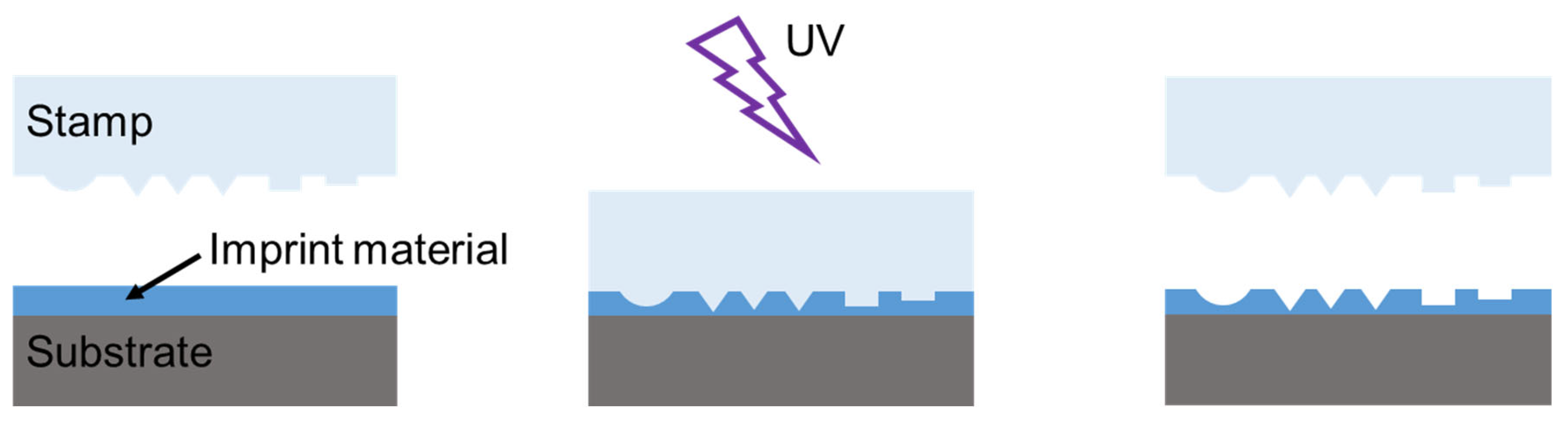
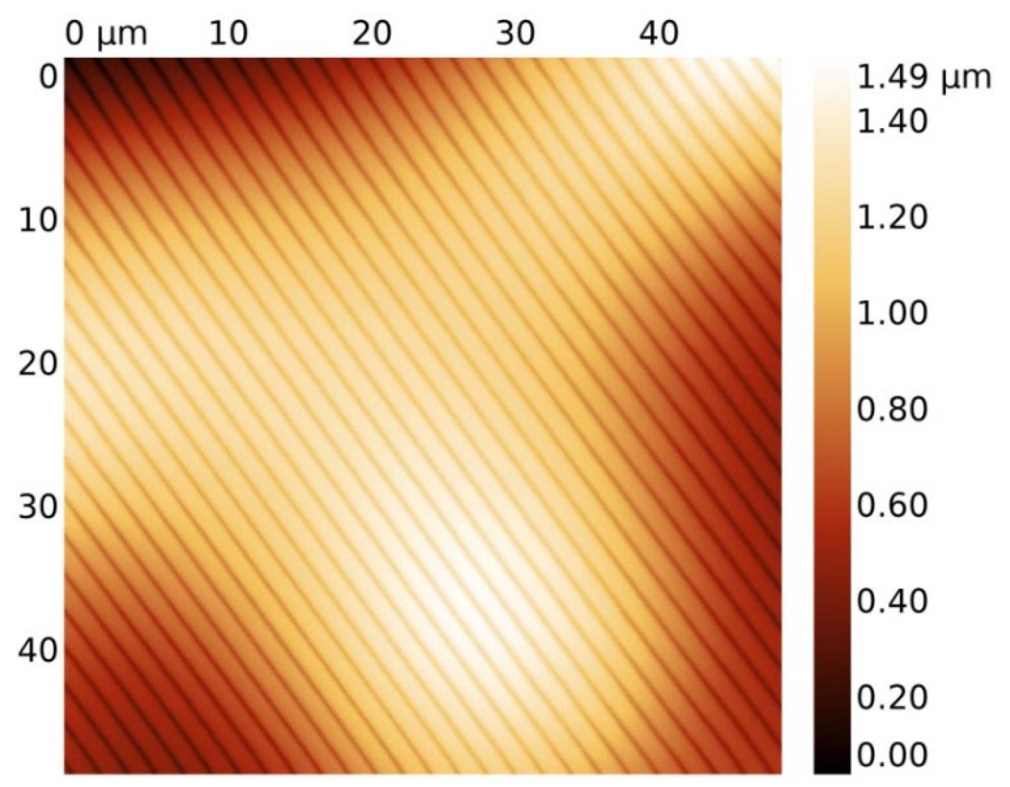
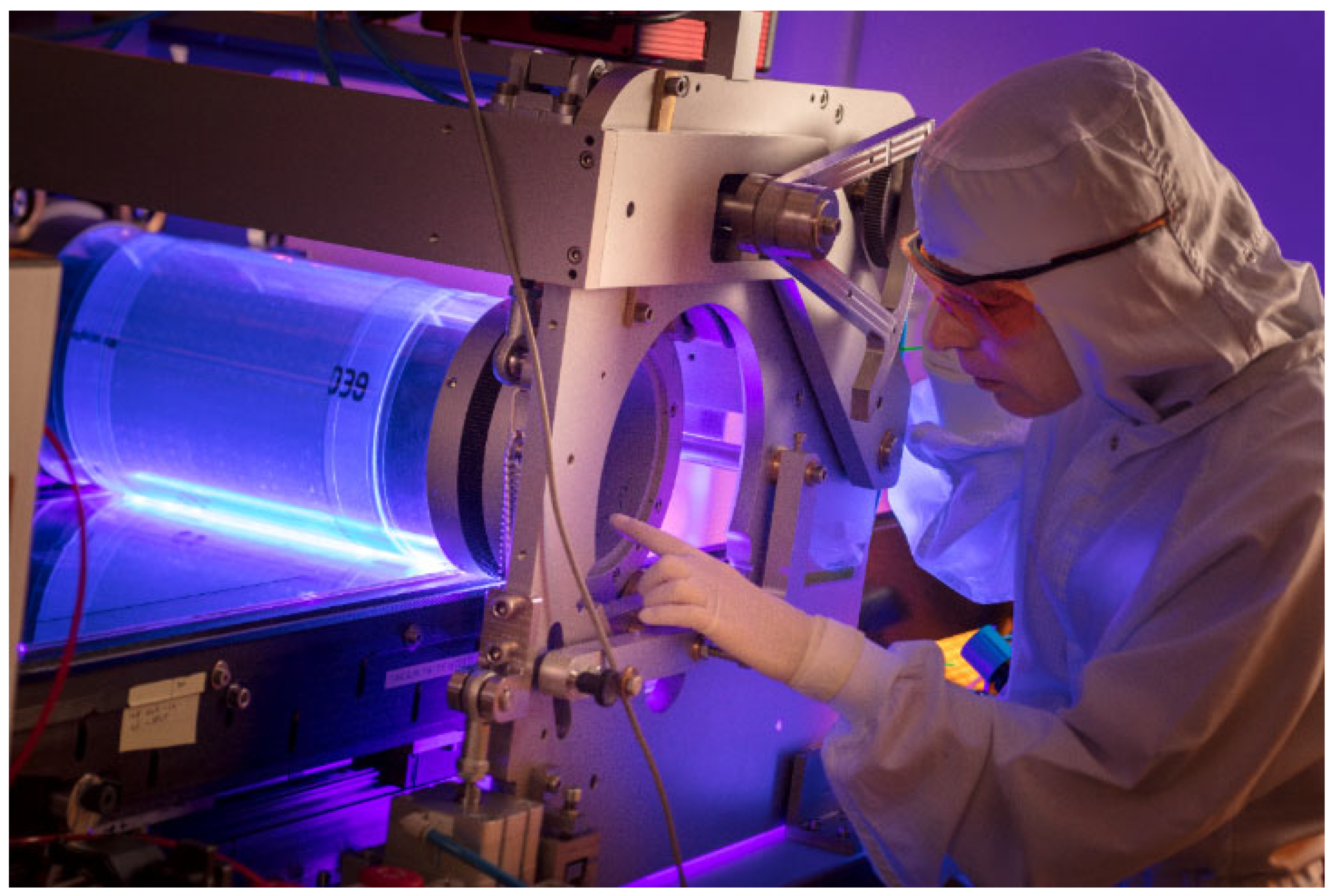
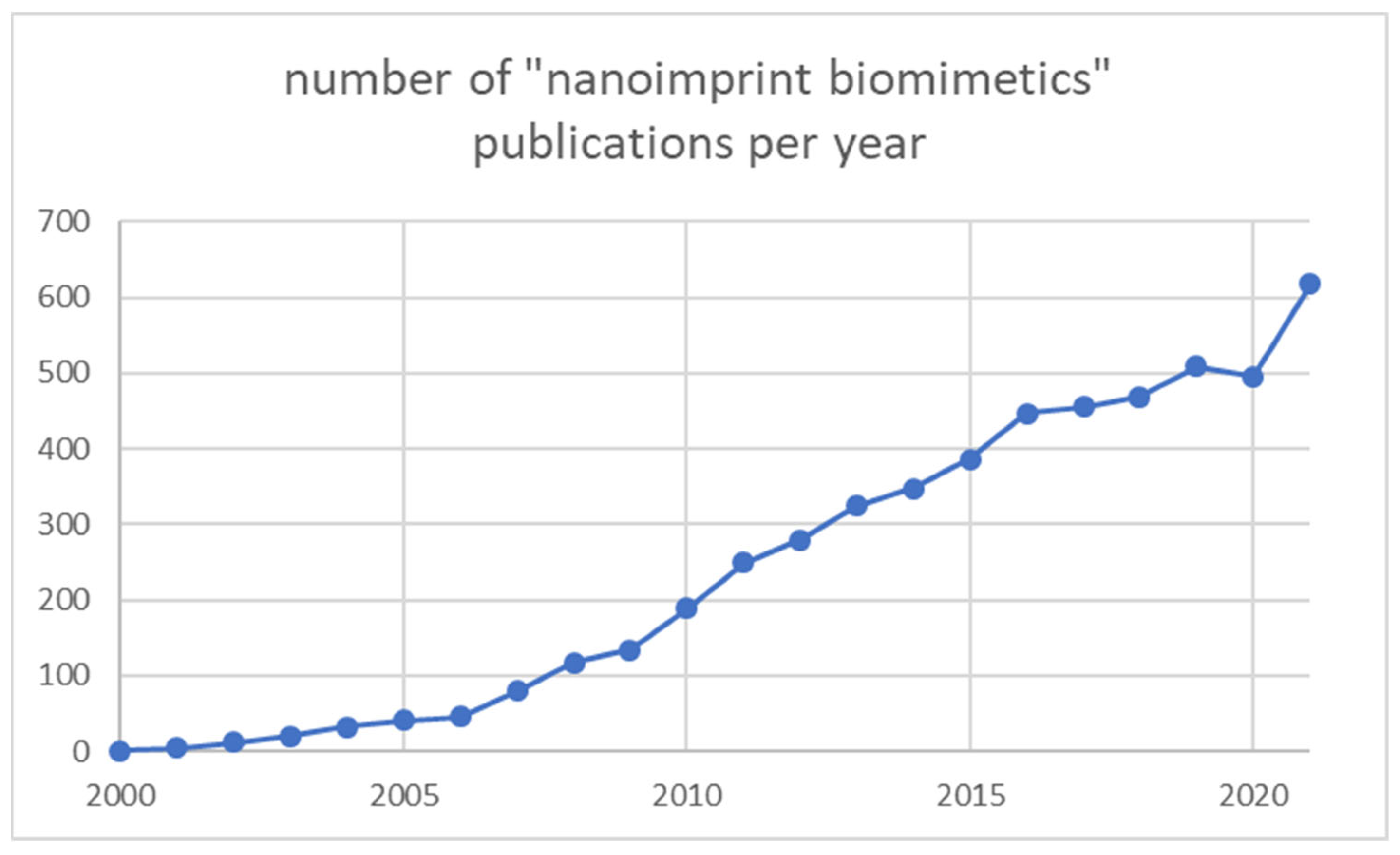
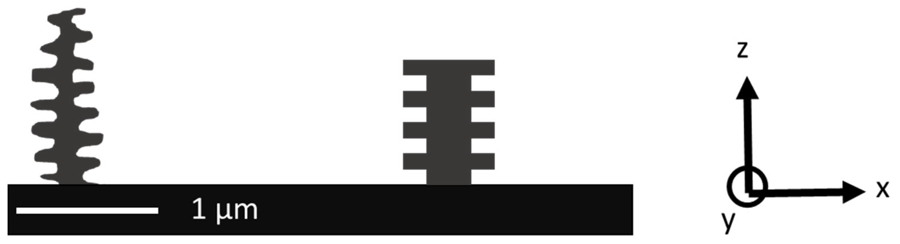
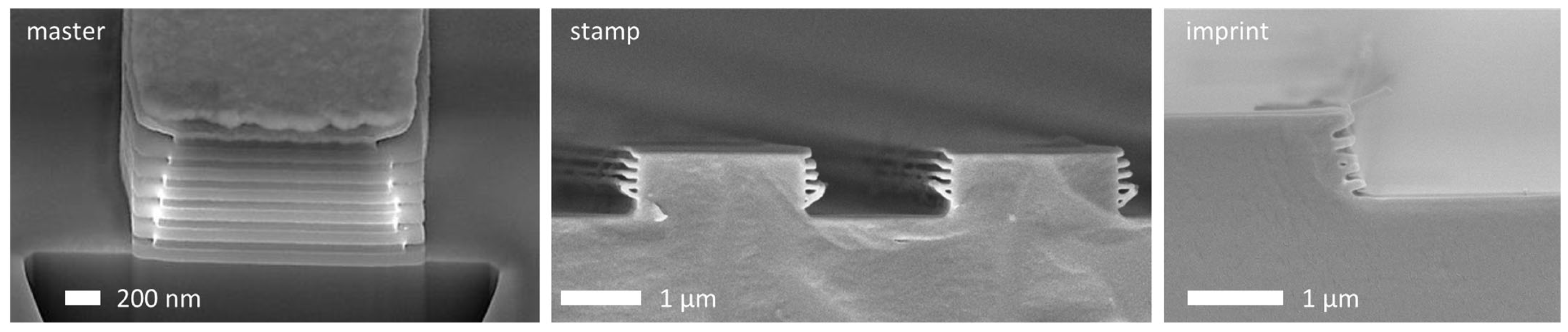
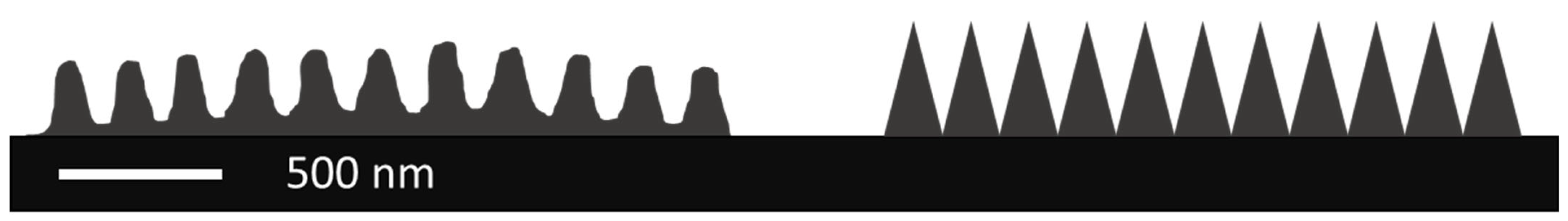
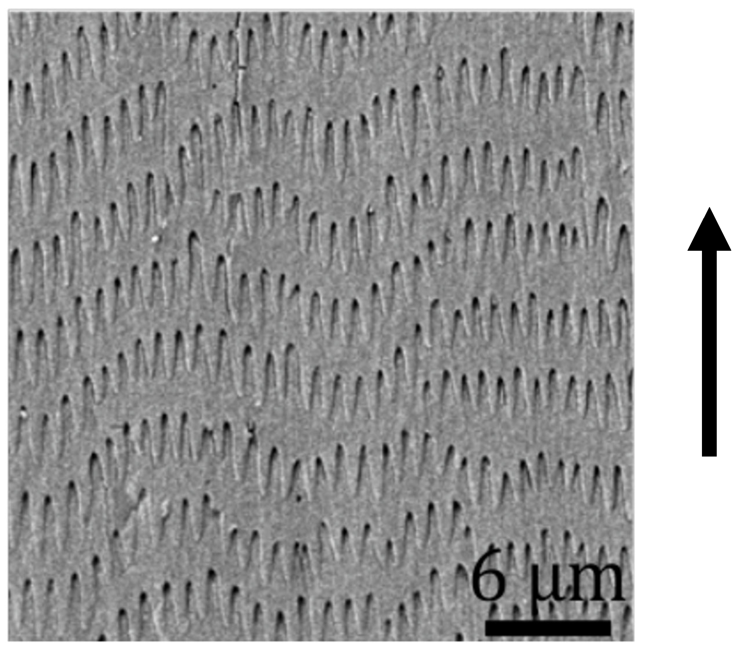
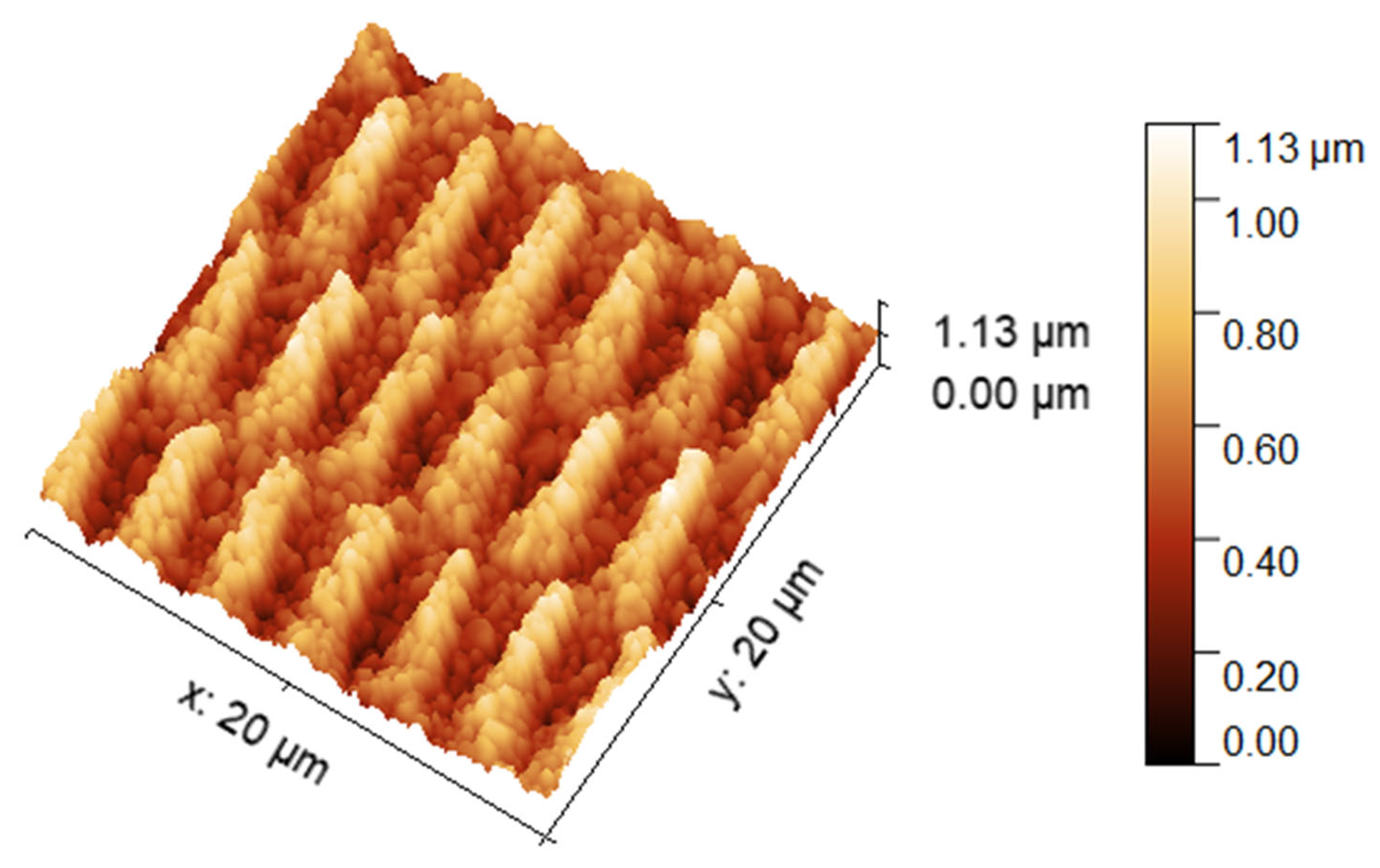
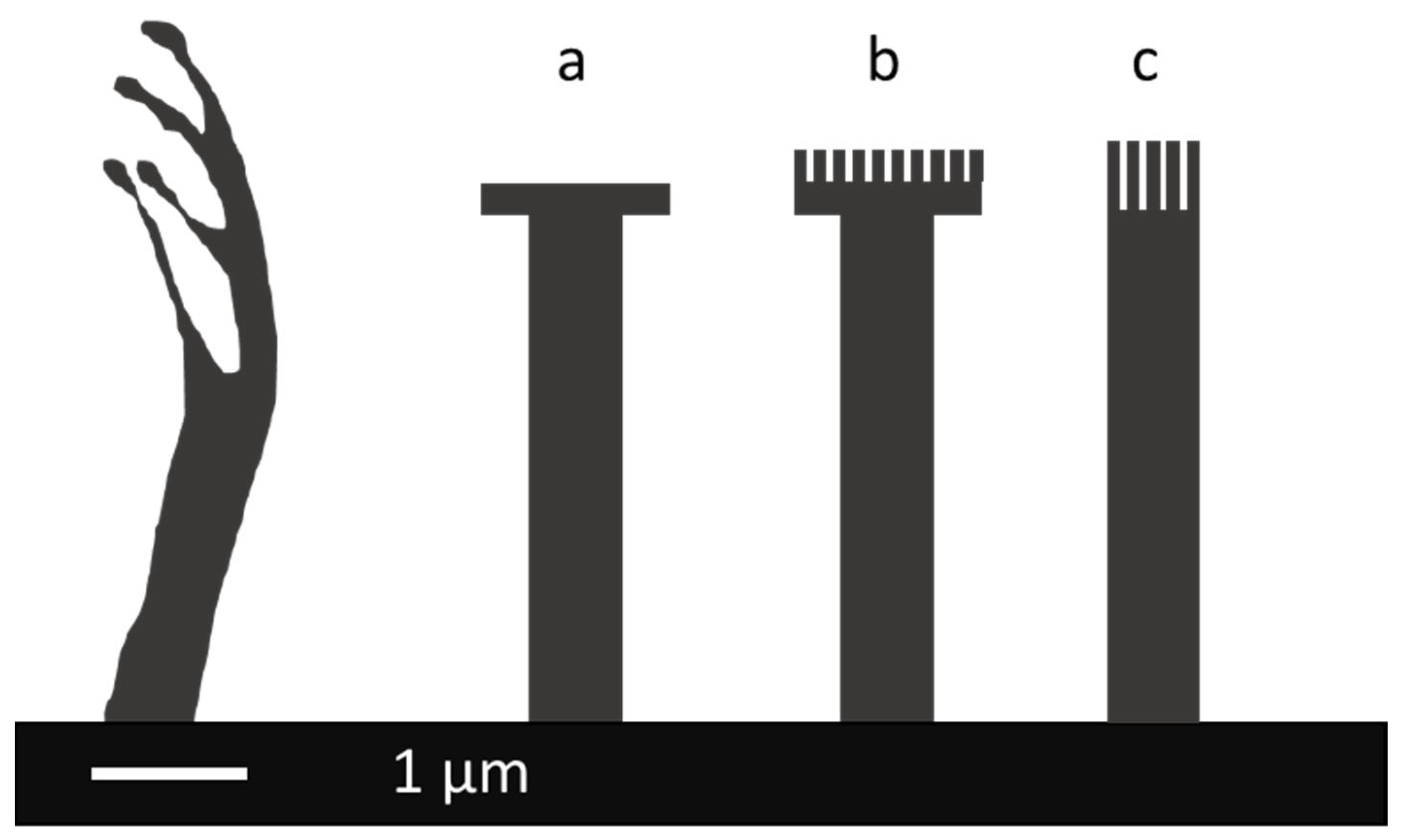
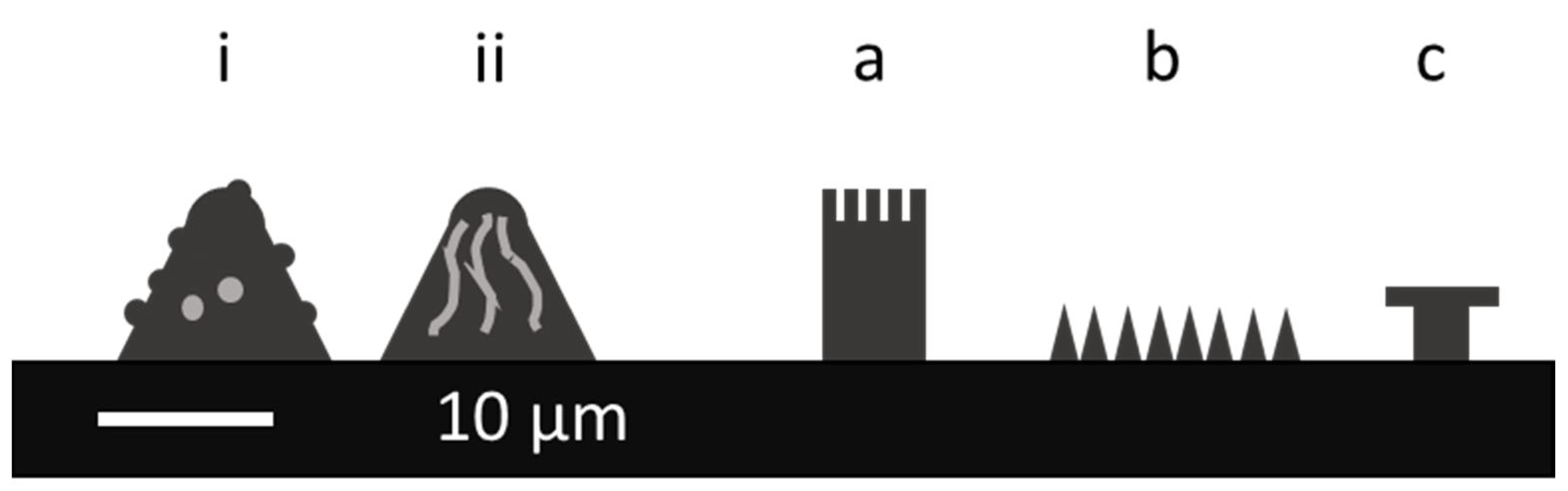
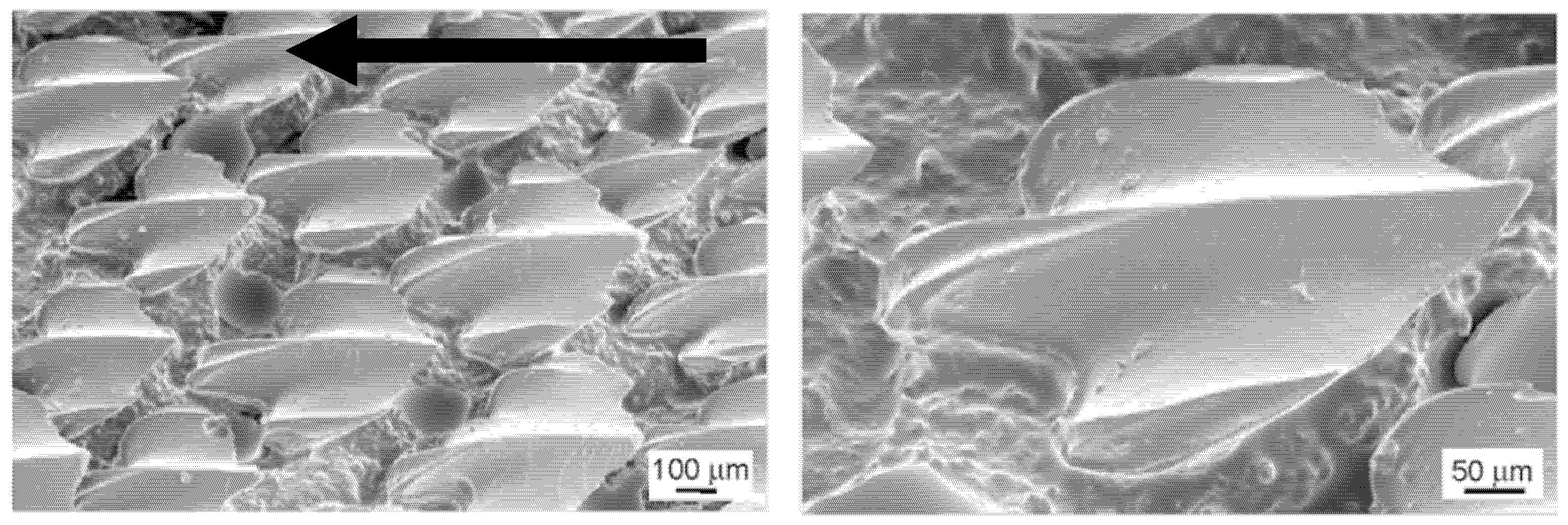
Table 1.
Examples for nanoimprinting of biomimetic structures for optical applications.
| Functionality | Inspiration | Features | Replication Process | References |
|---|---|---|---|---|
| Structural colors | Morpho butterfly | artificial | UV-NIL | [94,95] |
| artificial | UV-NIL | [97] | ||
| natural | epoxy casting | [99] | ||
| rose | natural | solvent assisted casting | [101,102] | |
| Antireflection structures | moth-eye | artificial | UV soft roller nanoimprint | [111] |
| R2P UV-NIL | [112,115] | |||
| R2R UV-NIL | [119] | |||
| UV-NIL | [33,120] | |||
| hot embossing | [116,117] | |||
| plants | natural | epoxy casting | [122] |
Table 2.
Examples for nanoimprinting of biomimetic structures for modifying the surface interaction with solids.
Table 2.
Examples for nanoimprinting of biomimetic structures for modifying the surface interaction with solids.
| Functionality | Inspiration | Features | NIL Process | References |
|---|---|---|---|---|
| Friction modification | snake skin | artificial | UV-NIL | [126] |
| epoxy casting | [124,129] | |||
| lotus leave | artificial | hot embossing | [130,131,132] | |
| natural | hot embossing | [134,135] | ||
| Adhesion | gecko foot | artificial | silicone casting | [141,143,145] |
| hot embossing | [144,146,148] | |||
| UV-NIL | [147] |
Table 3.
Examples for the use of nanoimprinting to fabricate surfaces that influence the interaction with liquids.
Table 3.
Examples for the use of nanoimprinting to fabricate surfaces that influence the interaction with liquids.
| Functionality | Inspiration | Features | NIL Process | Ref |
|---|---|---|---|---|
| Repelling of liquids | lotus | natural | thermal NIL | [43] |
| hot embossing | [163] | |||
| bamboo | natural | UV-NIL | [160] | |
| rose | natural | UV-NIL | [161] | |
| hot embossing | [162,164] | |||
| artificial | R2R UV-NIL | [165] | ||
| hot embossing | [164] | |||
| pitcher plants | artificial | R2R UV-NIL | [165] | |
| butterfly | natural | thermal NIL | [43] | |
| moth-eye | artificial | R2R UV-NIL | [112] | |
| hot embossing | [166,172] | |||
| UV+ thermal | [167] | |||
| springtail | artificial | reversal | [174] | |
| liquid guidance | pitcher plant | artificial | R2R | [180] |
| drag reduction | shark skin | natural | hot embossing | [184] |
| epoxy/PU casting | [182] | |||
| UV-NIL | [185] |
Table 4.
Examples for life science applications of biomimetic structures fabricated by nanoimprinting.
Table 4.
Examples for life science applications of biomimetic structures fabricated by nanoimprinting.
| Functionality | Inspiration | Features | NIL Process | References |
|---|---|---|---|---|
| cell growth | collagen fibers | natural | hot embossing | [199] |
| tissue engineering | Rubus fruticosus leaves | natural | hot embossing | [200] |
| antibacterial | moth-eye | UV-NIL | [210,211] | |
| cicada wing | natural | UV-NIL | [209] | |
| shark skin | natural | PDMS and PU casting | [183] | |
| UV-NIL | [185] | |||
| artificial | UV-NIL | [212] | ||
| PDMS casting | [213] |
Table 5.
Examples for energy related applications of biomimetic structures fabricated by nanoimprinting.
Table 5.
Examples for energy related applications of biomimetic structures fabricated by nanoimprinting.
| Functionality | Inspiration | Features | NIL Process | Reference |
|---|---|---|---|---|
| antireflection and light management for photovoltaics | moth-eye | artificial | reversal NIL | [220] |
| artificial | room temperature embossing | [118] | ||
| thermal NIL | [221] | |||
| rose petal | natural | hot embossing | [219] | |
| artificial | UV-NIL | [223] | ||
| current generation | lotus leave | natural | hot embossing | [222] |
Table 6.
Examples for mastering methods for artificial biomimetic structures.
| Mastering Technology | Inspiration | References |
|---|---|---|
| electron beam lithography | snake skin | [127] |
| rose petal | [224] | |
| optical lithography | shark skin | [214] |
| laser interference lithography | moth-eye | [111,203] |
| self-organized etching | moth-eye | [118] |
| gecko | [148,225] | |
| nanoparticle self-assembly + etching | moth-eye | [113,220] |
| additive manufacturing | gecko | [147] |
Publisher’s Note: MDPI stays neutral with regard to jurisdictional claims in published maps and institutional affiliations. |
© 2022 by the author. Licensee MDPI, Basel, Switzerland. This article is an open access article distributed under the terms and conditions of the Creative Commons Attribution (CC BY) license (https://creativecommons.org/licenses/by/4.0/).
Share and Cite
MDPI and ACS Style
Muehlberger, M. Nanoimprinting of Biomimetic Nanostructures. Nanomanufacturing 2022, 2, 17-40. https://doi.org/10.3390/nanomanufacturing2010002
AMA Style
Muehlberger M. Nanoimprinting of Biomimetic Nanostructures. Nanomanufacturing. 2022; 2(1):17-40. https://doi.org/10.3390/nanomanufacturing2010002
Chicago/Turabian StyleMuehlberger, Michael. 2022. "Nanoimprinting of Biomimetic Nanostructures" Nanomanufacturing 2, no. 1: 17-40. https://doi.org/10.3390/nanomanufacturing2010002