Article

Advances in CdZnTeSe for Radiation Detector Applications

1
Savannah River National Laboratory, Aiken, SC 29808, USA
2
Brookhaven National Laboratory, Upton, NY 11973, USA
*
Author to whom correspondence should be addressed.
Radiation 2021, 1(2), 123-130; https://doi.org/10.3390/radiation1020011
Submission received: 16 March 2021 / Revised: 5 April 2021 / Accepted: 8 April 2021 / Published: 25 April 2021

Abstract

:

Simple Summary

Cadmium-zinc-telluride is the most important semiconductor material today for room temperature gamma-ray detector applications. The radiation detectors are widely used for medical imaging, homeland security, and X- and gamma-ray astronomy. However, the material has longstanding technological problems. Despite significant improvements over the past 3 decades, the technology still suffers from major detrimental defects such as a high concentration of tellurium inclusions and sub-grain boundary network/dislocation walls, which adversely impact the yield of high-quality detectors fabricated from the crystals. To address these challenges, selenium was added to the cadmium zinc telluride matrix. The Se addition was found to have a profound effect to reduce the deleterious defects in the crystals. The resulting cadmium-zinc-telluride-selenide material was found to be free from a sub-grain boundary network with reduced tellurium inclusions. Thus, cadmium zinc telluride selenide material is a promising approach to increase the yield of high-quality radiation detectors as compared to cadmium zinc telluride. This paper reports a path to the advancement of the quaternary material to achieve the best detector performance. This advance may resolve the longstanding issues associated with cadmium zinc telluride-based X- and gamma-ray detectors.

Abstract

Detection of X- and gamma-rays is essential to a wide range of applications from medical imaging to high energy physics, astronomy, and homeland security. Cadmium zinc telluride (CZT) is the most widely used material for room-temperature detector applications and has been fulfilling the requirements for growing detection demands over the last three decades. However, CZT still suffers from the presence of a high density of performance-limiting defects, such as sub-grain boundary networks and Te inclusions. Cadmium zinc telluride selenide (CZTS) is an emerging material with compelling properties that mitigate some of the long-standing issues seen in CZT. This new quaternary is free from sub-grain boundary networks and possesses very few Te inclusions. In addition, the material offers a high degree of compositional homogeneity. The advancement of CZTS has accelerated through investigations of the material properties and virtual Frisch-grid (VFG) detector performance. The excellent material quality with highly reduced performance-limiting defects elevates the importance of CZTS as a potential replacement to CZT at a substantially lower cost.

1. Introduction

Radiation detectors, especially for the X- and gamma-ray range, are being developed and utilize the advantages of semiconductor radiation detectors operating at room temperature. These detectors have a large number of applications ranging from homeland security to medical imaging, astronomy, and high energy physics [1,2,3,4]. Intense global search has been carried out to develop efficient semiconductors with high detection efficiency at lower cost [4]. CdZnTe remains the leading material of choice today and has dominated the global market for more than three decades. However, the performance and yield of high-quality detector-grade materials are still limited by the presence of high concentrations of randomly distributed performance-limiting defects, such as Te inclusions and sub-grain boundary networks [5]. These defects act as trapping centers, severely hindering the localized charge transport and imposing severe spatial inhomogeneity in the charge transport characteristics of the detector, which adversely affects the device performance [5,6,7,8]. Cd1−xZnxTe1−ySey (CZTS), a new quaternary II–VI compound semiconductor material, has emerged as a next-generation detector material in the last few years and has the potential to surpass CZT at a lower cost due to its higher yield of high-quality detectors. The addition of selenium in the CZT matrix successfully circumvents many of the long-standing issues associated with the material [9,10], thus gaining attention for further studies by various groups [11,12,13,14,15,16]. The addition of selenium to CZT provides multipronged advantages over conventional CZT. The compositional homogeneity of Cd1−xZnxTe1−ySey has been found to increase significantly for ingots grown by both the traveling heater method (THM) and Bridgman method [9,10,11] as compared with CZT [17,18]. The addition of selenium in the CZT matrix has also been found to increase hardness, with reduced cadmium vacancy and significant reduction of Te inclusions with respect to CZT, plus the resulting CZTS materials have been found to be free from sub-grain boundary networks [9,10,19,20]. Various compositions with selenium concentrations of 1.5, 2, 4, and 7 atomic % have been studied while keeping Zn at 10 atomic % for all the compositions. The Cd1−xZnxTe1−ySey composition with x = 0.1 and y = 0.02 has been found to be optimal in terms of charge transport characteristics and device performance. In this article, we report the advancement of Cd1−xZnxTe1−ySey (x = 0.1, y = 0.02) by the THM technique and discuss the performance of Frisch-grid detectors fabricated from as-grown CZTS ingots.

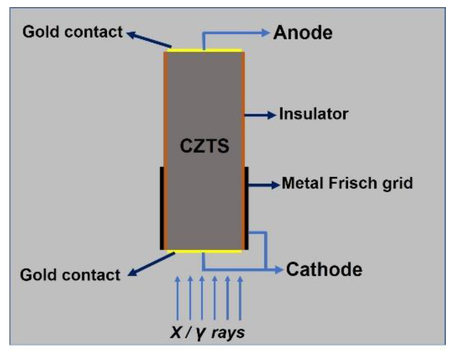
2. Methods and Materials

Indium-doped Cd0.9Zn0.1Te0.98Se0.02 ingots with 52 mm diameter were grown by the THM technique. The starting materials were 6N purity Cd0.9Zn0.1Te from 5N Plus Inc. and 6N purity CdSe from Azelis Inc. Tellurium was used as the solvent for the THM growth. Both 6N purity tellurium and 6N purity indium were procured from Alfa Aesar. The compound Cd0.9Zn0.1Te0.98Se0.02 was first synthesized from a stoichiometric amount of Cd0.9Zn0.1Te and CdSe in a 52 mm inner diameter ampoule. The inner wall of the ampoule was precoated with carbon film by cracking spectroscopic-grade acetone at 900 °C, followed by annealing at ~1150 °C. The synthesized material was used for the THM growth, which was carried out in carbon-coated 52 mm internal and 58 mm outer diameter quartz ampoules. The growth conditions were reported earlier [10,21] for the CZTS ingots. The optimization of the growth parameters mainly involved the fine-tuning of the height for the solution zone, which depends on parameters such as the amount of tellurium, growth temperature, temperature gradient, and translation speed [22].
The grown ingots were cut into pieces of desired sizes using a programmable diamond impregnated wire saw for further material characterization and device fabrication. The samples were then lapped on silicon carbide (SiC) papers subsequently polished on a felt pad using alumina suspensions of successive grit sizes. The final polishing was performed with 0.05 µm alumina suspension to obtain mirror-finished surfaces. Infrared (IR) transmission microscopic and X-ray topographic studies were performed using a Nikon Eclipse LV 100 Microscope and LBNL Advanced Light Source (ALS) Synchrotron Beamline 3.3.2 with an X-ray beam energy ranging from 4 to 25 keV, respectively. Virtual Frisch-grid (VFG) detector geometries were used to evaluate the detector performances fabricated from the as-grown Cd0.9Zn0.1Te0.98Se0.02 ingots. Figure 1 shows a schematic of the VFG detector configuration. The geometries of VFG detector samples in general have large aspect ratio parallelepiped bar shapes, as shown in Figure 1. Details of VFG detector geometry have been discussed earlier [23].
The side walls of the detector sample were wrapped with an insulator, Kapton tape in the present case. A metal strip of copper was wrapped on the insulating layer known as the Frisch grid, as illustrated in Figure 1. The end faces were coated with a metallic film, gold in the present investigation. The gold films acted as the anode and cathode contacts. The gold contacts on the anode and cathode faces were deposited by a gold chloride solution on as-polished CZTS surfaces. A higher leakage current was observed for bromine–methanol etched surfaces compared with as-polished surfaces. Thus, as-polished surfaces were chosen to fabricate the detectors to achieve a better signal-to-noise ratio because of the lower leakage current of the detector. The cathode and the metallic Frisch grid were electrically connected, and the cathode side was irradiated by different gamma sources to evaluate the detector response. The induced signal was registered through an eV Products preamplifier (A 4039), an Ortec 672 shaping amplifier, and MCA-3 series/P 7882 card from FAST ComTec. All the detector measurements were performed at room temperature in the range of 21–23 °C on as-grown Cd0.9Zn0.1Te0.98Se0.02 samples. All the results presented here are on as-grown material; no postgrowth thermal treatments were performed for the THM-grown CZTS samples.

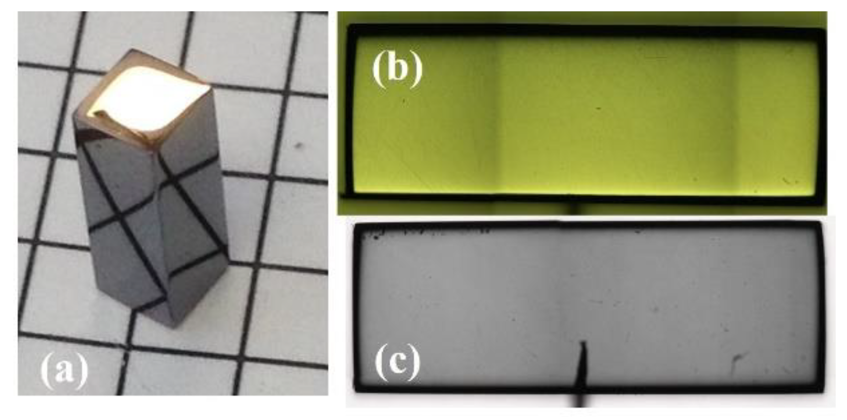
3. Results and Discussion

We have been developing CdZnTeSe detectors over the last 4 years and steadily improved the material quality and VFG detector performances. In the early phase of the research, we achieved an energy resolution in the range of ~1.3% to ~2% at 662 keV for the VFG detectors with a length of 9–10 mm fabricated from as-grown Cd0.9Zn0.1Te0.98Se0.02 ingots. Figure 2 summarizes some of the VFG detector performances fabricated from as-grown ingot, depicting all the detectors as having very few Te inclusions. The dimensions of the detectors are noted in the figure. The measured dark current density at 500 V obtained were 91, 49, 53, 63 pA/mm2 for the four devices, respectively and the resistivity values are in the range of ~1–3 × 10¹⁰ ohm-cm. The current densities for the three detectors out of four, were found to be reasonably uniform. Although all the detectors were fabricated from the same ingot, the observed variation of resistivity was reasonably large. However, the repeatability of the measured resistivity values varied for the same sample when refabricated using a similar surface preparation process. Similar effects were also observed for CZT samples. The operating bias voltages mentioned in Figure 2 were the optimum values for the corresponding detectors for the best energy resolution. The relatively wide variations of the energy resolutions, and optimum operating bias voltages suggest the presence of a fair amount of inhomogeneity in the grown ingot and surface properties of the detectors. Such wide variations of the electronic properties in CZT are very common due to randomly distributed high concentrations of sub-grain boundary networks and Te inclusions. However, due to the absence of sub-grain boundaries in CZTS material, the material uniformity and yield of high-resolution detectors were higher than CZT. Figure 3a shows the optical photograph of a typical bar detector with gold contact corresponding to the detector displayed in the bottom left corner of Figure 2. The detector dimensions are 3.4 × 3.6 × 9.7 mm3. Figure 3b,c shows scanned microscopic images of the detector in the reflection and IR transmission mode. As mentioned earlier, Figure 3c demonstrates the presence of very few Te inclusions, which can be considered a major achievement in the development of the quaternary compound CZTS. Modeling indicates that the presence of Te inclusions with concentrations of less than ~2 × 104 cm−3, ~3 × 103 cm−3, and ~7–8 × 102 cm−3 for 5, 10, and 15 µm sizes, respectively, in CZT material can be tolerated to achieve an energy resolution in the range of ~0.5%–0.6% at 662 keV [5]. In the present case for CZTS, the presence of very few Te inclusions suggests that the material is capable of producing very-high-energy-resolution detectors with higher yield as compared with CZT. Another major hurdle that CZT is facing is the presence of high concentrations of sub-grain boundary networks distributed randomly in the CZT matrix that evidently impose a significant impact on the detector performance [5]. This motivates the investigation of the sub-grain boundaries and their networks in CZTS. X-ray topography is perhaps the most powerful tool to explore the presence of sub-grain boundaries and their networks. In this present study, we conducted measurements using a synchrotron radiation source, especially in the reflection mode. Prior to the measurements, mirrorlike polished samples were etched in a 2% bromine–methanol solution for 2 min to remove any possible mechanically damaged layers that might have been produced during the polishing process. Sub-grain boundaries are essentially dislocations arranged in planes, which form dislocation walls, and their network is known as sub-grain boundary network. Such an isolated dislocation wall, namely, sub-grain boundary, is visible in Figure 4 along the arrow heads. Figure 4 depicts an X-ray topographic image of the whole detector shown in Figure 3a. As opposed to CZT, the topographic image of the CZTS detector is free from the presence of a sub-grain boundary network. The CZTS samples were consistently found to be free from a sub-grain boundary network for all the compositions with selenium concentrations between 1.5 and 7 at%. However, occasional presence of isolated sub-grain boundaries was observed [10,23]. These sub-grain boundary networks in CZT are known to degrade the detector response severely. Thus, the absence of a sub-grain boundary network in CZTS samples is highly promising and has the potential to increase the yield of very high-quality detectors from a given ingot. The production of sub-grain boundary-free CZTS material is an important improvement, which has otherwise been impossible to achieve for CZT due to its poor thermophysical properties near and below its melting point. The selenium plays an important role in the CZT matrix as an effective solid solution hardening agent.
The pulse height spectrum of the VFG detector for a 137Cs sealed source registered at room temperature under an applied bias of −1800 V and shaping time of 6 micro-second. is shown in Figure 5, revealing a well-resolved low-energy barium X-ray photopeak at ~32 keV and a characteristic 662 keV photopeak. Figure 5b is a magnified version of the spectrum to enhance the 662 keV photopeak. The energy at 662 keV was ~1.3% with a peak-to-valley ratio of ~20.
The overall performance of the as-grown CZTS detectors was observed to be excellent even at the early stage of our research. The underlying reason is the drastic reduction of performance-limiting defects as a result of the addition of selenium in the CZT matrix. The presence of high concentrations of sub-grain boundary networks and Te inclusions in CZT has been an unresolved major hurdle that restricts the yield of high-quality detector-grade material from grown ingots, resulting in a high cost of end products. The addition of selenium has been found to successfully alleviate many of the issues and enhance the potential for low-production cost. A continuous effort is being made to improve the material quality of the new quaternary material by optimizing the growth parameters. Within a short period of time, we have successfully improved the material properties and achieved as-measured energy resolutions in the range of 1 ± 0.1% at 662 keV for ~10 mm long VFG detectors [10,24]. The best energy resolution achieved with VFG CZTS detectors at room temperature thus far was ~0.77% at 662 keV without any charge-loss corrections. The profound improvements of the material quality of CZTS and detector performances within a span of about 4 years is very compelling. However, the new CZTS material still suffers from issues pertaining to impurity content. The impurities responsible for deep levels have been found to be very high in tens of ppb (parts per billion) as confirmed by glow discharge mass spectrometry (GDMS). These impurities in general have not been detectable in commercial CZT, except for Fe at ~22 ppba [25]. Table 1 lists the concentrations of some of the selected impurities present in two separate CZTS ingots. The presence of such high impurities in the CZTS matrix is believed to originate from the CdSe starting material. Thus, CZTS has room for further improvement of the material properties and the detector performance by purifying the starting materials.

4. Summary

The long-standing issues suffered by CZT pertaining to the presence of high concentrations of performance-limiting defects (sub-grain boundary network and Te inclusions) due to poor thermophysical properties motivated the researchers to find a suitable alternative material with better detector performance at a lower cost of production. We pursued an approach to improve CZT material properties by adding selenium to the matrix and discussed the advancement of CdZnTeSe. The effectiveness of adding selenium to the CdTe matrix was observed three decades ago by the infrared substrate community for night vision applications. The resulting ternary compound CdTeSe with as low as 0.4% Se was reported to be free from a sub-grain boundary network [26], while codoping with Zn and Se in the CdTe matrix was also observed to produce sub-grain boundary-free quaternary CdZnTeSe material [27]. The reported advantages of selenium addition to the CdTe/CZT matrix have motivated the development of CdZnTeSe for radiation detector applications. The optimum composition of the ternary compound (Cd0.9Zn0.1Te0.98Se0.02) has been determined for realizing the best detector performance. As discussed, in the early phase of the research, we attained an energy resolution in the range of ~1.3% to ~2% at 662 keV for the VFG detectors with a length of 9–10 mm fabricated from as-grown CZTS ingots. Within a short period of time, we have successfully improved the material properties, and very-high-energy-resolution VFG detectors have been achieved with average FWHM values of 1 ± 0.1% at 662 keV for ~10 mm long detectors [10,24]. The new compound CZTS has been found to be free from sub-grain boundary networks with very few Te inclusions embedded in the matrix, which improves the yield of high-quality detectors from the as-grown ingot with the potential of a significant reduction of detector cost. Achieving high-resolution detectors from as-grown CZTS in the early stage of our research reflects the efficacy of adding selenium to the CZT matrix due to the reduction of many performance-limiting defects. The quaternary CZTS has also been reported to be superior to CZT for some medical imaging applications, particularly those requiring a high flux of X-rays [14]. The observed high concentrations of external impurities suggest that further improvement of detector performances is possible through the growth of the quaternary material using purified starting materials. The material properties and the achieved detector performance supersede the present-day CZT material. Thus, the new material Cd0.9Zn0.1Te0.98Se0.02 with dramatically reduced defects offers tremendous potential to successfully replace CdZnTe material at a reduced cost.

Author Contributions

Conceptualization, U.N.R., R.B.J.; methodology, G.S.C., Y.C., U.N.R.; validation, G.S.C., Y.C., R.B.J.; investigation, writing—original draft preparation, U.N.R.; writing—review and editing, U.N.R., R.B.J., Y.C.; visualization, U.N.R., Y.C., G.S.C.; supervision, U.N.R., R.B.J. All the authors participated in scientific discussions and critically reviewed the manuscript. All authors have read and agreed to the published version of the manuscript.

Funding

This work was supported by the U.S. Department of Energy Office of Defense Nuclear Nonproliferation Research and Development (DNN R&D.) The authors from SRNL acknowledges the partial support from the Laboratory Directed Research and Development (LDRD) program within the Savannah River National Laboratory (SRNL). This document was prepared in conjunction with work accomplished under Contract No. DE-AC09-08SR22470 with the U.S. Department of Energy (DOE) Office of Environmental Management (EM).

Institutional Review Board Statement

Not applicable.

Informed Consent Statement

Not applicable.

Data Availability Statement

This study did not report any data.

Conflicts of Interest

The authors declare no conflict of interest.

References

  1. Schlesinger, T.E.; Toney, J.E.; Yoon, H.; Lee, E.Y.; Brunett, B.A.; Franks, L.; James, R.B. Cadmium zinc telluride and its use as a nuclear radiation detector material. Mater. Sci. Eng. R. 2001, 32, 103–189. [Google Scholar] [CrossRef]
  2. Yang, G.; James, R.B. Physics, Applications of CdTe, CdZnTe, and CdMnTe Radiation Detectors. In Defects, Hetero- and Nano-structures, Crystal Growth, Surfaces and Applications Part II; Triboulet, R., Siffert, P., Eds.; Elsevier: Amsterdam, The Netherlands, 2009; pp. 214–238. [Google Scholar]
  3. Del Sordo, S.; Abbene, L.; Caroli, E.; Mancini, A.M.; Zappettini, A.; Ubertini, P. Progress in the Development of CdTe and CdZnTe Semiconductor Radiation Detectors for Astrophysical and Medical Applications. Sensors 2009, 9, 3491–3526. [Google Scholar] [CrossRef] [PubMed]
  4. Johns, P.M.; Nino, J.C. Room temperature semiconductor detectors for nuclear security. J. Appl. Phys. 2019, 126, 040902-1-20. [Google Scholar] [CrossRef] [Green Version]
  5. Bolotnikov, A.E.; Camarda, G.S.; Cui, Y.; Yang, G.; Hossain, A.; Kim, K.; James, R.B. Characterization and evaluation of extended defects in CZT crystals for gamma-ray detectors. J. Cryst. Growth 2013, 379, 46–56. [Google Scholar] [CrossRef]
  6. Carini, G.A.; Bolotnikov, A.E.; Camarda, G.S.; James, R.B. High-resolution X-ray mapping of CdZnTe detectors. Nucl. Instrum. Methods Phys. Res. Sect. A Accel. Spectrometers Detect. Assoc. Equip. 2007, 579, 120–124. [Google Scholar] [CrossRef]
  7. Amman, M.; Lee, J.S.; Luke, P.N. Electron trapping nonuniformity in high-pressure-Bridgman-grown CdZnTe. J. Appl. Phys. 2002, 92, 3198–3206. [Google Scholar] [CrossRef] [Green Version]
  8. Camarda, G.S.; Bolotnikov, A.E.; Cui, Y.; Hossain, A.; Awadalla, S.A.; MacKenzie, J.; Chen, H.; James, R.B. Polarization Studies of CdZnTe Detectors Using Synchrotron X-Ray Radiation. IEEE Trans. Nucl. Sci. 2008, 55, 3725–3730. [Google Scholar] [CrossRef] [Green Version]
  9. Roy, U.N.; Camarda, G.S.; Cui, Y.; Gul, R.; Hossain, A.; Yang, G.; Zazvorka, J.; Dědič, V.; Franc, J.; James, R.B. Role of selenium addition to CdZnTe matrix for room-temperature radiation detector applications. Sci. Rep. 2019, 9, 1–7. [Google Scholar] [CrossRef] [Green Version]
  10. Roy, U.N.; Camarda, G.S.; Cui, Y.; Gul, R.; Yang, G.; Zazvorka, J.; Dedic, V.; Franc, J.; James, R.B. Evaluation of CdZnTeSe as a high-quality gamma-ray spectroscopic material with better compositional homogeneity and reduced defects. Sci. Rep. 2019, 9, 1–7. [Google Scholar] [CrossRef] [Green Version]
  11. Hwang, S.; Yu, H.; Bolotnikov, A.E.; James, R.B.; Kim, K. Anomalous Te Inclusion Size and Distribution in CdZnTeSe. IEEE Trans. Nucl. Sci. 2019, 66, 2329–2332. [Google Scholar] [CrossRef]
  12. Chaudhuri, S.K.; Sajjad, M.; Kleppinger, J.W.; Mandal, K.C. Charge transport properties in CdZnTeSe semiconductor room-temperature γ-ray detectors. J. Appl. Phys. 2020, 127, 1–8. [Google Scholar] [CrossRef]
  13. Chaudhuri, S.K.; Sajjad, M.; Kleppinger, J.W.; Mandal, K.C. Correlation of Space Charge Limited Current and γ-Ray Response of CdxZn1-xTe1-ySey Room-Temperature Radiation Detectors. IEEE Elect. Device Lett. 2020, 41, 1336–1339. [Google Scholar] [CrossRef]
  14. Yakimov, A.; Smith, D.J.; Choi, J.; Araujo, S.L. Growth and characterization of detector-grade CdZnTeSe by horizontal Bridgman technique. SPIE Proc. 2019, 11114. [Google Scholar] [CrossRef]
  15. Chanda, S.; Ghosh, D.; Debnath, B.; Debbarma, M.; Bhattacharjee, R.; Chattopadhyay, S. Calculations of the structural and optoelectronic properties of cubic CdxZn1−xSeyTe1−y semiconductor quaternary alloys using the DFT-based FP-LAPW ap-proach. J. Comp. Elect. 2020, 19, 1–25. [Google Scholar] [CrossRef]
  16. Rejhon, M.; Dědič, V.; Beran, L.; Roy, U.N.; Franc, J.; James, R.B. Investigation of Deep Levels in CdZnTeSe Crystal and Their Effect on the Internal Electric Field of CdZnTeSe Gamma-Ray Detector. IEEE Trans. Nucl. Sci. 2019, 66, 1952–1958. [Google Scholar] [CrossRef]
  17. Zhang, N.; Yeckel, A.; Burger, A.; Cui, Y.; Lynn, K.G.; Derby, J.J. Anomalous segregation during electrodynamic gradient freeze growth of cadmium zinc telluride. J. Cryst. Growth 2011, 325, 10–19. [Google Scholar] [CrossRef]
  18. Roy, U.N.; Weiler, S.; Stein, J.; Cui, Y.; Groza, M.; Buliga, V.; Burger, A. Zinc mapping in THM grown detector grade CZT. J. Cryst. Growth 2012, 347, 53–55. [Google Scholar] [CrossRef]
  19. Franc, J.; Moravec, P.; Dědič, V.; Roy, U.; Elhadidy, H.; Minárik, P.; Šíma, V. Microhardness study of Cd1-x ZnxTe1-ySey crystals for X-ray and gamma ray detectors. Mater. Today Commun. 2020, 24, 1–5. [Google Scholar] [CrossRef]
  20. Gul, R.; Roy, U.N.; Camarda, G.S.; Hossain, A.; Yang, G.; Vanier, P.; Lordi, V.; Varley, J.; James, R.B. A comparison of point defects in Cd1−xZnxTe1−ySey crystals grown by Bridgman and traveling heater methods. J. Appl. Phys. 2017, 121, 1–7. [Google Scholar] [CrossRef]
  21. Roy, U.N.; Gueorguiev, A.; Weiller, S.; Stein, J. Growth of spectroscopic grade Cd0.9Zn0.1Te:In by THM technique. J. Cryst. Growth 2009, 312, 33–36. [Google Scholar] [CrossRef]
  22. Roy, U.N.; Burger, A.; James, R.B. Growth of CdZnTe crystals by the traveling heater method. J. Cryst. Growth 2013, 379, 57–62. [Google Scholar] [CrossRef]
  23. Kargar, A.; Jones, A.M.; McNeil, W.J.; Harrison, M.J.; McGregor, D.S. CdZnTe Frisch collar detectors for γ-ray spectroscopy. Nucl. Instrum. Methods Phys. Res. A 2006, 558, 497–503. [Google Scholar] [CrossRef]
  24. Roy, U.N.; Camarda, G.S.; Cui, Y.; James, R.B. High-resolution virtual Frisch grid gamma-ray detectors based on as-grown CdZnTeSe with reduced defects. Appl. Phys. Lett. 2019, 114. [Google Scholar] [CrossRef]
  25. McCoy, J.J.; Kakkireni, S.; Gilvey, Z.H.; Swain, S.K.; Bolotnikov, A.E.; Lynn, K.G. Overcoming Mobility Lifetime Product Limitations in Vertical Bridgman Production of Cadmium Zinc Telluride Detectors. J. Electron. Mater. 2019, 48, 4226–4234. [Google Scholar] [CrossRef]
  26. Rudolph, P. Fundamental studies on Bridgman growth of CdTe. Prog. Cryst. Growth Charact. 1994, 29, 275–381. [Google Scholar] [CrossRef]
  27. Tanaka, A.; Masa, Y.; Seto, S.; Kawasaki, T. Zinc and selenium co-doped CdTe substrates lattice matched to HgCdTe. J. Cryst. Growth 1989, 94, 166–170. [Google Scholar] [CrossRef]
Figure 1. Schematic diagram of a virtual-grid CZTS detector.
Radiation 01 00011 g001
Figure 2. Performance of Frisch-grid detectors fabricated from the same THM-grown ingot.
Radiation 01 00011 g002
Figure 3. (a) Optical photograph of the as-grown CZTS bar detector with gold contact, (b) microscopic scanned image of the detector in reflection mode, and (c) microscopic scanned image of the detector in IR transmission mode. Detector dimensions: 3.4 × 3.6 × 9.7 mm3.
Radiation 01 00011 g003
Figure 4. X-ray topographic image of an as-grown detector. Detector dimensions: 3.4 × 3.6 × 9.7 mm3.
Radiation 01 00011 g004
Figure 5. (a) Pulse height spectrum of the VFG detector for a 137Cs source and (b) a magnified version of the same spectrum to enhance the 662 keV peak. Detector dimensions: 3.4 × 3.6 × 9.7 mm3.
Radiation 01 00011 g005
Table 1. Selected impurity concentrations present in two different THM-grown Cd0.9Zn0.1Te0.98Se0.02 ingots as measured by GDMS.
ElementsCZTS Ingot #1CZTS Ingot #2
Concentration (ppb at.)Concentration (ppb at.)
Fe4242
Cu<422
Ti<5<5
Cr36<20
Pb1110
Ni16<4
Sn<100<100
Publisher’s Note: MDPI stays neutral with regard to jurisdictional claims in published maps and institutional affiliations.

