Article

A Systematic Method for Scaling Coefficients of the Continuous-Time Low-Pass ΣΔ Modulator Using a Simulink-Based Toolbox

Electronics and Electrical Communications Engineering Department, Ain Shams University, Cairo 11517, Egypt
*
Author to whom correspondence should be addressed.
Eng 2024, 5(1), 1-16; https://doi.org/10.3390/eng5010001
Submission received: 31 October 2023 / Revised: 3 December 2023 / Accepted: 14 December 2023 / Published: 19 December 2023
(This article belongs to the Section Electrical and Electronic Engineering)

Abstract

:
The sigma-delta modulator (SDM) is one of the well-established data converter architectures. It is well-known for achieving a high signal-to-noise ratio (SNR). In the SDM, the integrators in the loop filter could suffer from overloading if the signal swing exceeds its maximum level, which leads to performance and SNR degradation. Thus, scaling the system coefficients is needed, such that there is no overloading for the integrators. In this work, we present a systematic general method that could be used for scaling the signal swings in the continuous-time low-pass sigma-delta modulator (SDM). The proposed method can be applied to any continuous-time low-pass SDM architecture, and it includes the scaling of all the possible combinations of the system coefficients. Moreover, an open-source Simulink-based toolbox that includes the systematic method is presented. This toolbox could help the designer to execute the scaling process and the simulations in an efficient way. In addition to that, a design example is discussed to illustrate the proposed method, wherein the presented toolbox is used for simulations, and the simulation results are shown.

1. Introduction

The sigma-delta modulator (SDM) is the most commonly used data converter in high-precision applications. It can perform high-resolution data conversion using the oversampling and noise-shaping techniques. There is a recent trend nowadays to use the sigma-delta modulator in high-speed applications. For such applications, the continuous-time sigma-delta modulator is widely used. The continuous-time sigma-delta modulator is preferred over the discrete-time sigma-delta modulator due to its higher speed and its lower power consumption [1,2].
In continuous-time sigma-delta modulators, the integrators could suffer from overloading if the output signal swing exceeds the full-scale limit. This overloading causes degradation in the performance of the modulator that can be noticed when implementing the circuits, wherein the signal is clipped if its swing is larger than the full-scale limit. Therefore, one important step in the system-level design of the SDM is to perform scaling for the system coefficients, such that the integrators’ output swings are within the full-scale limit, so that there is no overloading [3,4].
Figure 1 shows a general third-order continuous-time low-pass sigma-delta modulator. It includes all the possible system coefficients. It includes feedforward coefficients (“k” coefficients), input feedforward coefficients (“b” coefficients), resonators (“g” coefficients), and feedback DAC coefficients (“a” coefficients). There are two types of coefficients that are included: the resistive types (ending with ”R”) and the capacitive types (ending with “C”). For the feedback DACs, each one can be either a resistive DAC or a current DAC. The third-order SDM includes three integrators. Each integrator supports three input paths: including resistive input paths (R), capacitive input paths (C), and DAC input paths (D). It also includes an adder block and a quantizer block. The quantizer can be a single-bit or a multi-bit quantizer. This general third-order SDM is used for illustration in this work; however, the same concepts can be applied to any other order.
Several methods for SDM coefficient scaling have been published before. A systematic method for scaling integrators’ output swings in sigma-delta modulators has been proposed in [5]. Another systematic method for scaling integrators’ output swings in resonator-based continuous-time sigma-delta modulators has been proposed in [6]. Moreover, another method for scaling the feedback coefficients of continuous-time sigma-delta modulators has been proposed in [7]. These methods can be used to scale integrators’ output swings by scaling the system coefficients, while preserving both the signal transfer function (STF) and the noise transfer function (NTF). However, these methods still have some limitations.
First, every one of these methods discusses only one specific filter type of the sigma-delta modulator, either SDM with feedback filter architecture or SDM with feedforward filter architecture. However, various published designs tend to have a hybrid architecture, including both feedforward and feedback coefficients at the same time, which helps to reduce the STF peaking while ensuring that the integrators’ output swing is not large [8,9,10,11,12,13]. Such hybrid architecture was not included in the previous three methods. Second, they do not include the scaling technique for the input feedforward coefficients (“b” coefficients), which have been used in some recent designs [14,15,16]. Third, they do not include the scaling technique for the capacitive-type coefficients, which have been used in several published sigma delta modulators [17,18,19,20,21]. Fourth, they only include the simplest integrator model (1/S), but they do not include other models for the integrator, such as the opamp-based RC integrator with a series resistor and capacitor in the feedback network, which has been used in multiple SDM designs [22,23,24,25,26,27], or the one with a parallel resistor and capacitor in the feedback network, which has been used in some SDM designs [28,29]. Fifth, they do not include the method of adjusting the signal swing at the input of the quantizer, which is needed to avoid the overloading of the quantizer. Sixth, none of these methods discussed the trade-off between the integrator output swing and the linearity specification of the integrator.
With respect to the tools for the automation of this scaling process, one well-known option is the MATLAB-based Schreier Delta-Sigma toolbox [30]. It can perform the scaling of the coefficients automatically to adjust the signal swings, and it generates the scaled coefficients. However, it has the same limitations mentioned before in previous scaling methods, with the exception that it includes the option to scale the input feedforward coefficients (“b” coefficients).
In this work, a systematic general method for the scaling of the signal swings in the continuous-time low-pass sigma-delta modulator is proposed. This method overcomes the limitations mentioned before. First, the proposed method is a generic method that could be applied to any SDM architecture, including the scaling of all the possible system coefficients (feedforward coefficients, feedback coefficients, and resonators). Second, it includes the scaling technique of the input feedforward coefficients (“b” coefficients). Third, it provides the scaling method for capacitive-type coefficients in addition to resistive-type coefficients. Fourth, it includes various integrator models that are not included in the previous reported methods, such as the opamp-based RC integrator with a series resistor and capacitor in the feedback network, or the one with a parallel resistor and capacitor in the feedback network. Fifth, it includes the option of adjusting the signal swing at the input of the quantizer. Sixth, it includes the non-linearity effect of the integrator to deduce the trade-off between the integrator output swing and the integrator non-linearity.
Moreover, an open-source MATLAB and Simulink-based toolbox has been included in this work (link in the references section) [31]. This toolbox can be easily used to simulate continuous-time sigma-delta modulators and to scale signal swings, with the proposed systematic method included inside the toolbox. The user can enter the system coefficients, simulate the system, and deduce the needed scaling of the swings. Then, he can select the scaling factor needed for each block, and the new coefficients will be calculated automatically. Hence, this toolbox greatly aids in automating the process of scaling SDM system coefficients.
The paper is organized as follows: In Section 2, the integrator block is discussed in detail, presenting the different models included for the integrator and discussing integrator non-linearity modelling after that. In Section 3, the proposed systematic method for scaling the integrators’ output swings, and the proposed method for adjusting the signal swing at the input of the quantizer are both presented. In Section 4, a design example is discussed for illustration, and the toolbox simulation results are shown. Section 5 concludes the paper.

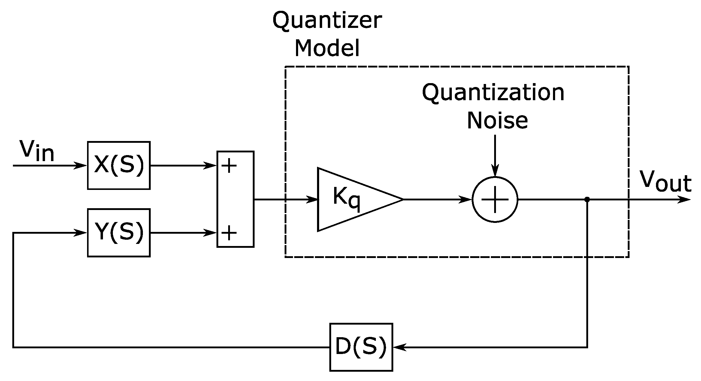
2. Modelling of the Integrator

Before discussing the proposed systematic scaling method, it is crucial to first discuss the model of the integrator that can be used in the continuous-time low-pass SDM. The proposed toolbox, accompanied by the proposed systematic method, includes various models for the opamp-based RC integrator. The integrator model can generally support resistive input path, capacitive input path, and DAC input path. The DAC could be a current DAC or a resistive DAC. Regarding the integrator feedback network, the included designs have three types of the feedback networks: a capacitor, a capacitor with a series resistor, and a capacitor with a parallel resistor.
Figure 2 shows a simplified schematic of the family of opamp-based RC integrator designs included in the study. A summary of the included designs of the opamp-based RC integrator is presented in Table 1. The definitions of the main circuit parameters related to Figure 2 are shown in Table 2. The output expressions of the included designs of the opamp-based RC integrator are shown in Table 3. The negative sign due to the inverting gain of the single-ended opamp-based RC integrator is neglected for simplicity. It is worth mentioning that the opamp is assumed to be ideal for simplicity because non-idealities, such as its finite gain and bandwidth do not have any significant effect on the system coefficients scaling process. Table 4 includes the definitions of the input coefficients used in the equations mentioned in Table 3. Table 5 includes the definitions of some parameters used in the equations mentioned in Table 3.
Figure 3 shows the simplified general diagram of the model of the integrator. There are three types of input paths: the resistive input path, capacitive input path, and the DAC input path (which can be either current DAC or resistive DAC). There is a transfer function block for each one of the three paths based on the derived equations from (2) to (7). The model also includes a saturation block which includes the option of swing limitation beyond a certain threshold. Moreover, it has the option to include the non-linearity effect of the opamp. This will be discussed in the next paragraph.
One important thing that was not included in the previous methods [5,6,7] is the non-linearity effect of the opamp gain used in the integrator. In real circuits, as the output swing of the integrator becomes large (even within the allowed full-scale limit), the output impedance of the opamp can be affected due to the change in the available headroom on the CMOS transistors, and hence the gain of the opamp can vary with the output swing level. Such non-linearity in the opamp gain leads to harmonic distortion and degradation in the SNDR (Signal to Noise and Distortion Ratio). Thus, it is important to include such an effect in the integrator model to see the non-linearity effect versus the output swing level.
Equations (14) and (15) describe the transfer function of this block given that the input is within the full-scale limit. Ideally (i.e., with no included non-linearity), the output equals the input. However, by including the non-linearity effect, there will be a smooth gain compression in the transfer function.
The term (α) represents the non-linearity. If its value is zero, this means that the block is perfectly linear (non-linearity is not included). As its value becomes larger than zero, this means more non-linearity. Figure 4 shows the characteristics of this block for different values of (α). In this graph, both the input and the output are normalized over the full- scale limit.
V o u t = V i n   ;   if   α = 0  
V o u t = 1   tanh ( α ) tanh ( α V i n )   ;   if   α 0  

3. Proposed Systematic Method for Scaling the Signal Swings

3.1. Proposed Method for Scaling the Integrators’ Output Swings

Now, after discussing the model of the integrator, the general idea of the scaling method of the integrator’s output swing is discussed here. Figure 5 shows the general basic concept of this method. If it is desired to scale the integrator output swing by factor (F), all the input paths of the integrator are scaled by the factor (F), and all the paths connected to the output of the integrator are scaled by (1/F). There are three input paths of the integrators: the resistive input path, the capacitive input path, and the DAC input path. The paths connected to the output of the integrator are the resistive path and the capacitive path. By using this scaling method, the signal transfer function (STF) and the noise transfer function (NTF) of the SDM are not affected at all.

3.2. Proposed Method for Adjusting the Quantizer Input Signal Swing

In addition to the scaling of the integrator output swing, this paper presents a method to adjust the signal swing at the input of the quantizer. For adjusting the signal swing at the input of the quantizer, all the input paths to the quantizer are scaled by the factor (Fq), and all the paths connected to the output of the quantizer (which are the feedback DACs) are scaled by (1/Fq).
This proposed method has no effect on the noise transfer function (NTF). However, it has an effect on the signal transfer function (STF). The whole STF is scaled by the factor (Fq). Therefore, for example, if the signal swing at the input of the quantizer is scaled by (Fq = 0.7), the STF magnitude will be multiplied by 0.7, which means that its magnitude will decrease by 3 dB and the SNR will decrease by 3 dB.
Figure 6 shows the simplified diagram of the original SDM before adjusting the quantizer input signal swing. The quantizer is modelled as a gain block (Kq) (wherein Kq is the gain of the quantizer) and the quantization noise is added after it. The STF and NTF of the system can be deduced using th diagram below, and they are given by (16) and (17).
S T F = X S K q 1 + D S K q Y S
N T F = 1 1 + D S K q Y S
If the input path of the quantizer is scaled by (Fq), and the output path of the quantizer is scaled by (1/Fq), the new simplified diagram of the modified SDM is shown in Figure 7. The new STF and NTF of the system can be deduced using the diagram below, and they are given by (18) and (19).
S T F   a f t e r   i n c l u d i n g   F q = X S K q F q 1 + 1 F q D S K q F q Y S = X S K q F q 1 + D S K q Y S
N T F   a f t e r   i n c l u d i n g   F q = 1 1 + 1 F q D S K q F q Y s = 1 1 + D S K q Y S
It is clear from the previous equations that the NTF will remain unchanged, while the STF will change. For the STF, the denominator remains the same, while the numerator is multiplied by the factor (Fq).
It is important to mention that adjusting the signal swing at the input of the quantizer (using Fq) is not exactly linear; this is because the quantizer is a non-linear block in reality. Furthermore, it is also worth mentioning that using the scaling factor (Fq) could lead to a very small change in the output swings of the integrators. That can be noticed in the design example discussed later.

3.3. Summary of the Scaling Factors

By applying the proposed methods mentioned above to the general third-order SDM shown in Figure 1, Table 6 presents a summary. This table shows the scaling factor of each coefficient in the SDM, wherein (F1) is the scaling factor of the first integrator output swing, (F2) is the scaling factor of the second integrator output swing, (F3) is the scaling factor of the third integrator output swing, and (Fq) is the factor used for adjusting the quantizer input signal swing. The third-order SDM is used for illustration; however, the same concept can be applied to any other order.

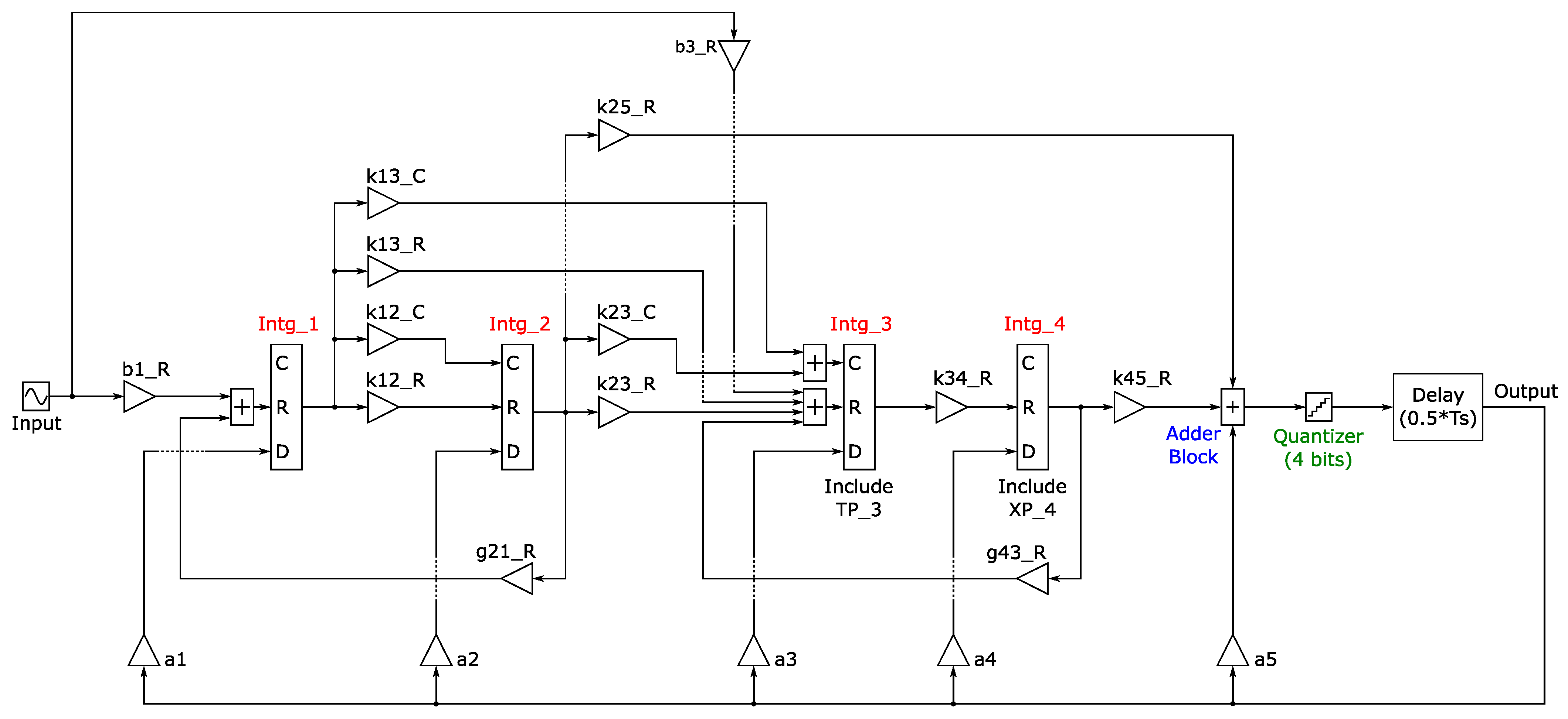
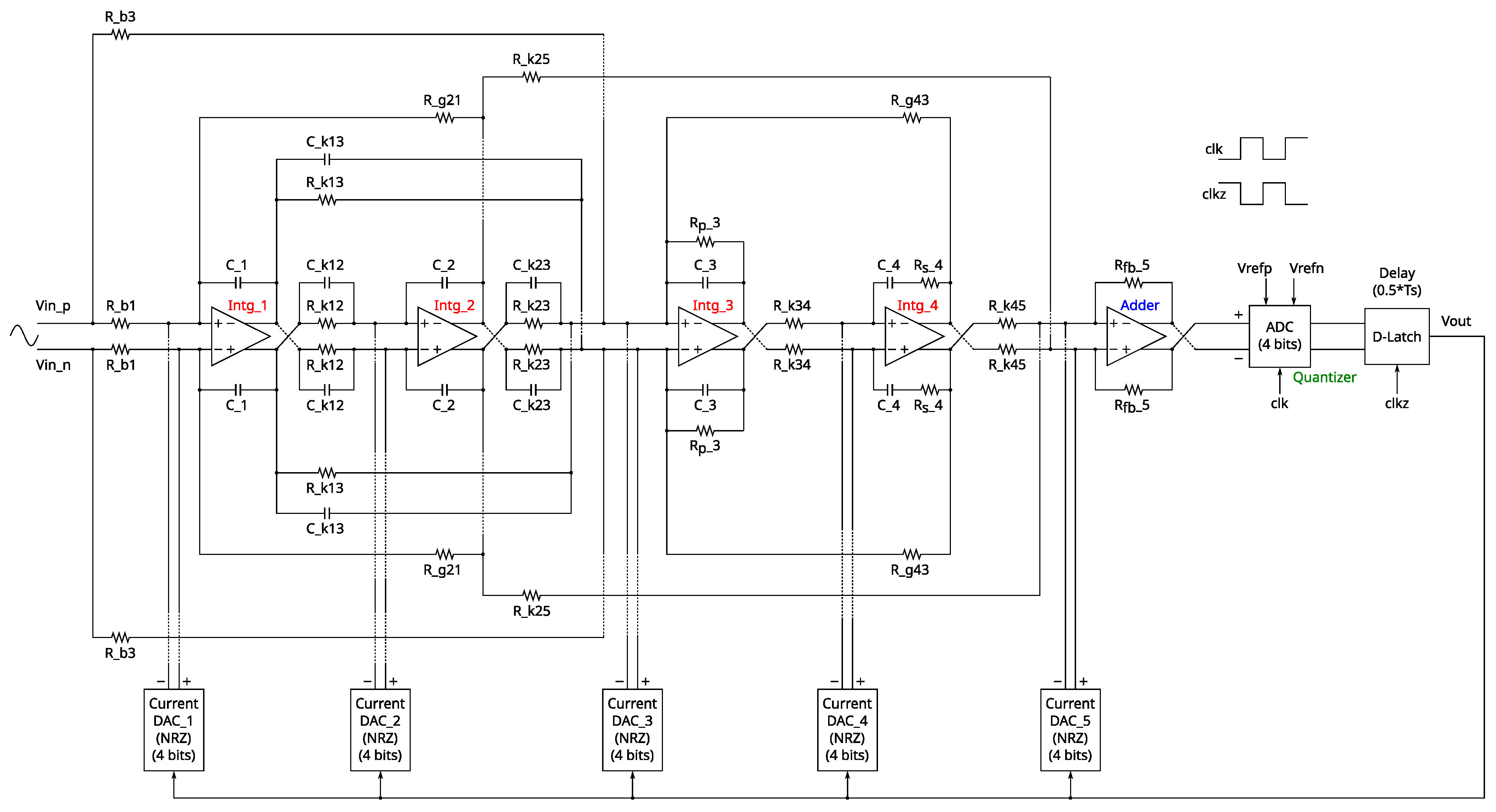
4. Design Example and Simulation Results

4.1. Design Example

For further illustration, a design example is discussed here. The proposed method is applied to a fourth-order SDM. The presented Simulink-based toolbox was used to perform the simulations and the scaling required. Figure 8 shows the simplified diagram of the design example. Figure 9 shows the detailed equivalent circuit diagram. It is a fourth-order continuous-time low-pass sigma-delta modulator with both feedforward coefficients and feedback current DACs. There are four integrators. Each of the first and the second integrators is an opamp-based RC integrator having a capacitor in the feedback network, and its output equation can be defined as mentioned in (2). The third integrator is an opamp-based RC integrator with a resistor parallel to the capacitor in the feedback network, and its output can be defined as mentioned before in (6). The fourth integrator is an opamp-based RC integrator having a series resistor with the capacitor in the feedback network, and its output can be defined as mentioned before in (4). Two types of coefficients are used: the resistive-type and the capacitive-type. There are two resistive-type resonators as well. A multi-bit quantizer is used (4 bits) in this modulator. A delay (0.5 Ts) is included after the quantizer to model the delay of the D-latch that follows the quantizer. The used oversampling ratio (OSR) is 16. Table 7 shows the values of the coefficients of the design example before performing the scaling.

4.2. Simulation Conditions and Observing the Swings

To simulate the SDM, an input signal whose amplitude equals 70% of the full scale is used for testing. Table 8 shows the normalized signals swings (i.e., normalized over the full-scale limit) in the SDM before performing any scaling. It is clear that the output swings of the integrators need to be scaled. It can also be noticed that the signal swing at the input of the quantizer needs to be adjusted.

4.3. Applying the Proposed Scaling Method

Applying the proposed systematic method to this fourth-order design example, the scaling factor of each coefficient in the SDM can be deduced as shown in Table 9, wherein (F1), (F2), (F3), (F4) are the scaling factors of the first integrator output swing, the second integrator output swing, the third integrator output swing, and the fourth integrator output swing, respectively. The term (Fq) is the factor used for adjusting the quantizer input signal swing.

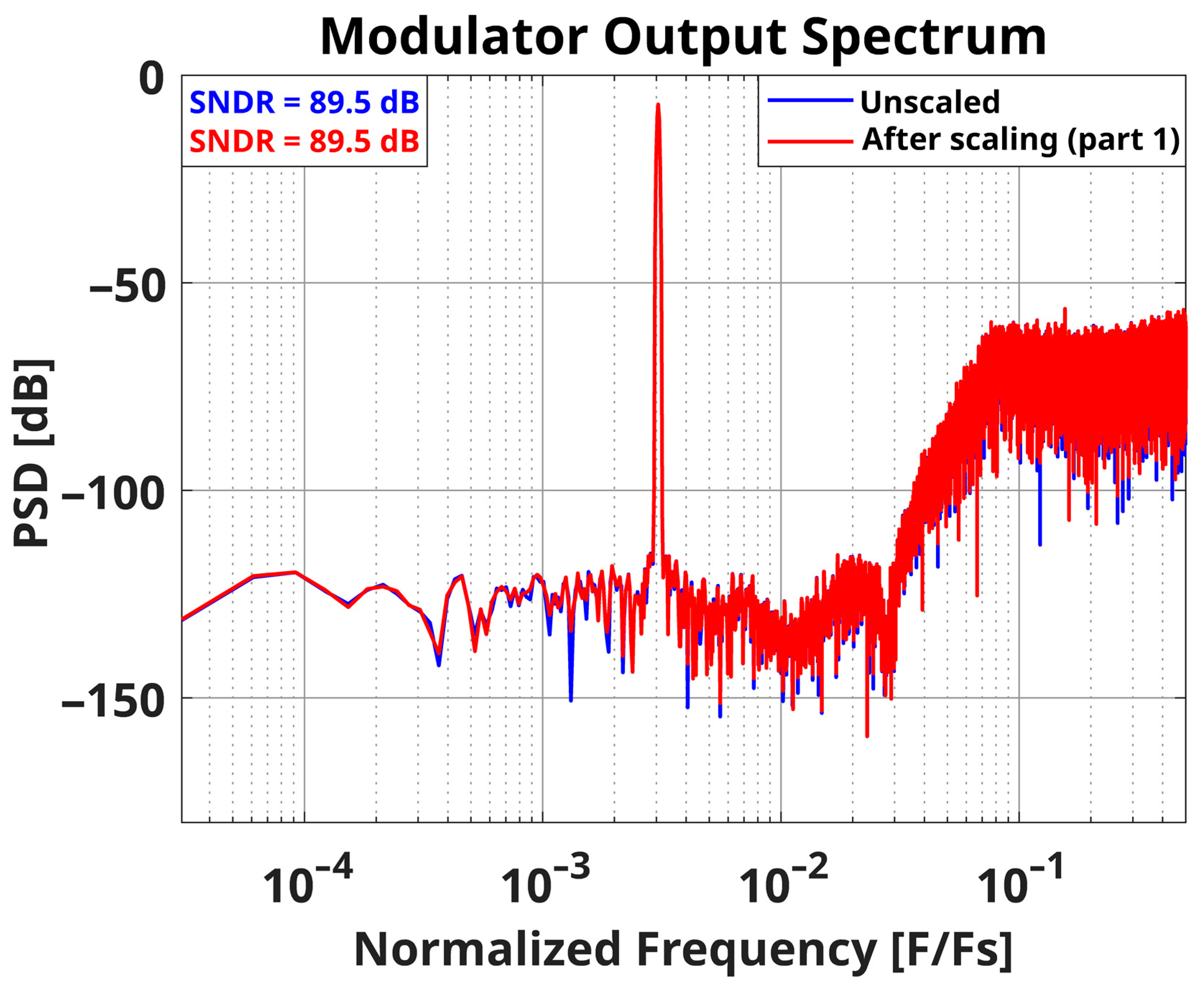
4.4. Simulations and Verification of Swing Scaling

The verification of the swing scaling is divided into three parts. In the first part of the verification, the scaling of the output swings of the integrators is verified alone without adjusting the signal swing at the input of the quantizer. In the second part of the verification, adjusting the signal swing at the input of the quantizer is verified alone, without scaling the output swings of the integrators. In the third part of the verification, the two concepts are verified together. These concepts are scaling the output swings of the integrators and adjusting the signal swing at the input of the quantizer.
Table 10 shows the normalized signal swings before scaling for the original SDM, the scaling factors used for each block, and the normalized swings after the scaling in each part of the verification.
Figure 10 shows the spectrum of the output of the modulator before and after the scaling in the first part of the verification. It is clear that the spectrum is identical in the two cases. Comparing the SNDR before and after the scaling in this part, it remains around 89.5 dB. This means that the STF and NTF remain unchanged.
Figure 11 shows the spectrum of the output of the modulator before and after the scaling in the second part of the verification. Figure 12 shows the spectrum of the output of the modulator before and after doing the scaling in the third part of the verification. From these two parts, it is clear that the spectrum after scaling is identical to the unscaled version except that the magnitude of the signal itself is decreased. Since the signal swing at the input of the quantizer is scaled by 0.7 (−3 dB) (using Fq = 0.7), the STF magnitude is scaled by the same value. As a result, the signal magnitude will decrease by 3 dB, which means that the SNDR will degrade by 3 dB. Comparing the SNDR before and after performing the scaling, the SNDR equals 86.5 dB after scaling in the second and in the third part of the verification, whereas it was 89.5 dB before scaling. This agrees with the deduced Equations (18) and (19).

4.5. Simulations and Verification of Integrator Non-linearity

In SDM, the first integrator is the most critical block for linearity, whereas the other following integrators are less critical. This is because any error due to the non-linearity of the second, third, and fourth integrators is divided by the gain of the previous stages when referring to the input, making it negligible compared to the error resulting from the first integrator.
In this part of the verification, the non-linearity effect of the first integrator is shown. Different values (0.3, 0.4, 0.5, 0.6) of the non-linearity coefficient (α) of the first integrator are simulated twice. The first simulation is performed using (F1 = 0.25), and the second simulation is performed using (F1 = 0.5). The values of (F2), (F3), (F4), and (Fq) are kept at 0.25, 0.25, 0.25, and 0.7, respectively, during the two tests.
Figure 13 shows the SNDR of the SDM versus the non-linearity coefficient (α) of the first integrator. The tradeoff between the non-linearity of the first integrator and its output swing is shown. It can be concluded that as the output swing of the integrator becomes smaller (F1 becomes smaller), the SNDR is better for the same value of the non-linearity coefficient (α).

5. Conclusions

This paper presents a systematic method for scaling the signal swings in the low-pass continuous-time sigma-delta modulator. This method overcomes the limitations mentioned in the previous reported methods. Moreover, a MATLAB and Simulink-based toolbox has been included in this work. The toolbox can be easily used to simulate the continuous-time sigma-delta modulators and to scale the signal swings. The analysis of the proposed method was discussed in detail. Furthermore, a design example was discussed for illustration, and the toolbox simulation results were presented.
In summary, Table 11 shows a comparison between this work and the previously published research.

Author Contributions

Conceptualization, B.M.Z.; Methodology, B.M.Z.; Validation, B.M.Z.; Formal analysis, B.M.Z.; Investigation, B.M.Z.; Resources, B.M.Z.; Writing—original draft, B.M.Z. and M.A.H.; Writing—review and editing, B.M.Z. and M.A.H.; Visualization, M.A.H.; Supervision, H.A.O. and H.A.E. All authors have read and agreed to the published version of the manuscript.

Funding

This research received no external funding.

Institutional Review Board Statement

Not applicable.

Informed Consent Statement

Not applicable.

Data Availability Statement

Conflicts of Interest

The authors declare no conflict of interest.

References

  1. Jain, A.; Venkatesan, M.; Pavan, S. Analysis and design of a high speed continuous-time ΔΣ modulator using the assisted OPAMP technique. IEEE J. Solid-State Circuits 2012, 47, 1615–1625. [Google Scholar] [CrossRef]
  2. Caldwell, T.; Alldred, D.; Schreier, R.; Shibata, H.; Dong, Y. Advances in high-speed continuous-time Delta-sigma modulators. In Proceedings of the IEEE 2014 Custom Integrated Circuits Conference, San Jose, CA, USA, 15–17 September 2014. [Google Scholar] [CrossRef]
  3. de La, R.J.M. Sigma-Delta Converters Practical Design Guide, 2nd ed.; Chapter 2; Wiley-IEEE Press: Hoboken, NJ, USA, 2019. [Google Scholar]
  4. Pavan, S.; Schreier, R.; Temes, G.C. Understanding Delta-Sigma Data Converters, 2nd ed.; Chapter 8; Wiley: Hoboken, NJ, USA, 2017. [Google Scholar]
  5. Beilleau, N.; Aboushady, H.; Louerat, M.M. Systematic approach for scaling coefficients of discrete-time and continuous-time sigma-delta modulators. In Proceedings of the 46th Midwest Symposium on Circuits and Systems 2003, Cairo, Egypt, 27–30 December 2003. [Google Scholar] [CrossRef]
  6. Yazkurt, U.; Dundar, G.; Talay, S.; Beilleau, N.; Aboushady, H.; de Lamarre, L. Scaling input signal swings of overloaded integrators in resonator-based sigma-delta modulators. In Proceedings of the 13th IEEE International Conference on Electronics, Circuits and Systems, Nice, France, 10–13 December 2006. [Google Scholar] [CrossRef]
  7. Zorn, C.; Brückner, T.; Ortmanns, M.; Mathis, W. State scaling of continuous-time sigma-delta modulators. Adv. Radio Sci. 2013, 11, 119–123. [Google Scholar] [CrossRef]
  8. Silva, P.; Huijsing, J. High-Resolution IF-to-Baseband Sigma delta ADC for Car Radios; Chapter 4; Springer: Dordrecht, The Netherlands, 2008. [Google Scholar]
  9. Briseno-Vidrios, C.; Edward, A.; Shafik, A.; Palermo, S.; Silva-Martinez, J. A 75-MHz continuous-time sigma-delta modulator employing a broadband low-power highly efficient common-gate summing stage. IEEE J. Solid-State Circuits 2017, 52, 657–668. [Google Scholar] [CrossRef]
  10. Wu, S.-H.; Kao, T.-K.; Lee, Z.-M.; Chen, P.; Tsai, J.-Y. A 160MHz-BW 72dB-DR 40mW continuous-time ΔΣ modulator in 16nm CMOS with analog ISI-reduction technique. In Proceedings of the 2016 IEEE International Solid-State Circuits Conference (ISSCC), San Francisco, CA, USA, 31 January–4 February 2016. [Google Scholar] [CrossRef]
  11. Huang, J.-F.; Lai, Y.-C.; Lai, W.-C.; Liu, R.-Y. Chip design of a low-voltage wideband continuous-time sigma-delta modulator with DWA technology for WiMAX Applications. Circuits Syst. 2011, 02, 201–209. [Google Scholar] [CrossRef]
  12. Andersson, M.; Anderson, M.; Sundstrom, L.; Mattisson, S.; Andreani, P. A 9MHz filtering ADC with additional 2nd-order ΔΣ modulator noise suppression. In Proceedings of the ESSCIRC (ESSCIRC), Bucharest, Romania, 16–20 September 2013. [Google Scholar] [CrossRef]
  13. Mitteregger, G.; Ebner, C.; Mechnig, S.; Blon, T.; Holuigue, C.; Romani, E. A 20-mW 640-MHz CMOS Continuous-Time ΣΔ ADC With 20-MHz Signal Bandwidth, 80-dB Dynamic Range and 12-bit ENOB. IEEE J. Solid-State Circuits 2006, 41, 2641–2649. [Google Scholar] [CrossRef]
  14. Song, S.; Lee, J.; Roh, J. A 20-MHz bandwidth, 75-dB dynamic range, continuous-time delta-sigma modulator with reduced nonidealities. Int. J. Circuit Theory Appl. 2019, 47, 1370–1380. [Google Scholar] [CrossRef]
  15. Liu, H.; Xing, X.; Gielen, G. A 0-dB STF-Peaking 85-MHz BW 74.4-dB SNDR CT ΔΣ ADC With Unary-Approximating DAC Calibration in 28-nm CMOS. IEEE J. Solid-State Circuits 2021, 56, 287–297. [Google Scholar] [CrossRef]
  16. Llimós Muntal, P.; Jørgensen, I.H.; Bruun, E. A continuous-time delta-sigma ADC for portable ultrasound scanners. Analog. Integr. Circuits Signal Process. 2017, 92, 393–402. [Google Scholar] [CrossRef]
  17. Xiao, Y.; Lu, Z.; Ren, Z.; Peng, X.; Tang, H. A 100-Mhz Bandwidth 80-dB Dynamic Range Continuous-Time Delta-Sigma Modulator with a 2.4-GHz Clock Rate. Nanoscale Res. Lett. 2020, 15, 58. [Google Scholar] [CrossRef] [PubMed]
  18. Ho, S.; Lo, C.L.; Ru, J.; Zhao, J. A 23 mW, 73 dB dynamic range, 80 MHz BW continuous-time delta-sigma modulator in 20 nm CMOS. In Proceedings of the 2014 Symposium on VLSI Circuits Digest of Technical Papers, Honolulu, HI, USA, 10–13 June 2014. [Google Scholar] [CrossRef]
  19. Shu, Y.S.; Tsai, J.Y.; Chen, P.; Lo, T.Y.; Chiu, P.C. A 28fJ/conv-step CT ΔΣ modulator with 78dB DR and 18MHz BW in 28nm CMOS using a highly digital multibit quantizer. In Proceedings of the 2013 IEEE International Solid-State Circuits Conference Digest of Technical Papers, San Francisco, CA, USA, 17–21 February 2013. [Google Scholar] [CrossRef]
  20. Zhang, J.; Yao, L.; Lian, Y. A 1.2-V 2.7-mW 160MHz continuous-time delta-sigma modulator with input-feedforward structure. In Proceedings of the 2009 IEEE Custom Integrated Circuits Conference, San Jose, CA, USA, 13–16 September 2009. [Google Scholar] [CrossRef]
  21. Prefasi, E.; Paton, S.; Hernandez, L.; Gaggl, R.; Wiesbauer, A.; Hauptmann, J. A 0.08 mm2, 7mW time-encoding oversampling converter with 10 bits and 20MHz BW in 65nm CMOS. In Proceedings of the 2010 ESSCIRC, Seville, Spain, 14–16 September 2010. [Google Scholar] [CrossRef]
  22. Cho, J.-K.; Woo, S. A 6-mW, 70.1-dB SNDR, and 20-MHz BW Continuous-Time Sigma-Delta Modulator Using Low-Noise High-Linearity Feedback DAC. IEEE Trans. Very Large Scale Integr. (VLSI) Syst. 2017, 25, 1742–1755. [Google Scholar] [CrossRef]
  23. Bolatkale, M.; Breems, L.J.; Rutten, R.; Makinwa, K.A. A 4GHz CT ΔΣ ADC with 70dB DR and -74dBFS THD in 125MHz BW. In Proceedings of the 2011 IEEE International Solid-State Circuits Conference, San Francisco, CA, USA, 20–24 February 2011. [Google Scholar] [CrossRef]
  24. Andersson, M.; Sundström, L.; Anderson, M.; Andreani, P. Theory and design of a CT ΔΣ modulator with low sensitivity to loop-delay variations. Analog. Integr. Circuits Signal Process. 2013, 76, 353–366. [Google Scholar] [CrossRef]
  25. Ho, C.-Y.; Lee, Z.-M.; Huang, M.-C.; Huang, S.-J. A 75.1dB SNDR, 80.2dB DR, 4th-order feed-forward continuous-time sigma-delta modulator with hybrid integrator for silicon TV-tuner application. In Proceedings of the IEEE Asian Solid-State Circuits Conference, Jeju, Republic of Korea, 14–16 November 2011. [Google Scholar] [CrossRef]
  26. Vadipour, M.; Chen, C.; Yazdi, A.; Nariman, M.; Li, T.; Kilcoyne, P.; Darabi, H. A 2.1 mW/3.2mW delay-compensated GSM/WCDMA Sigma Delta analog-digital converter. In Proceedings of the 2008 IEEE Symposium on VLSI Circuits, Honolulu, HI, USA, 18–20 June 2008. [Google Scholar] [CrossRef]
  27. Keller, M.; Buhmann, A.; Sauerbrey, J.; Ortmanns, M.; Manoli, Y. A comparative study on excess-loop-delay compensation techniques for continuous-time Sigma-Delta Modulators. IEEE Trans. Circuits Syst. I Regul. Pap. 2008, 55, 3480–3487. [Google Scholar] [CrossRef]
  28. Wang, W.; Chan, C.-H.; Zhu, Y.; Martins, R.P. A 100-MHz BW 72.6-dB-SNDR CT ΔΣ Modulator Utilizing Preliminary Sampling and Quantization. IEEE J. Solid-State Circuits 2020, 55, 1588–1598. [Google Scholar] [CrossRef]
  29. Dhanasekaran, V.; Gambhir, M.; Elsayed, M.M.; Sanchez-Sinencio, E.; Silva-Martinez, J.; Mishra, C.; Chen, L.; Pankratz, E. A 20MHz BW 68dB DR CT ΔΣ ADC based on a multi-bit time-domain quantizer and feedback element. In Proceedings of the 2009 IEEE International Solid-State Circuits Conference—Digest of Technical Papers, San Francisco, CA, USA, 8–12 February 2009. [Google Scholar] [CrossRef]
  30. Delta Sigma Toolbox. Available online: https://www.mathworks.com/matlabcentral/fileexchange/19-delta-sigma-toolbox (accessed on 31 October 2023).
  31. Link of the Proposed Toolbox. Password of the File: Bishoy@123! Available online: https://github.com/Bishoy-Milad-Zaky/SDM-Scaling-Toolbox (accessed on 15 December 2023).
Figure 1. Simplified general diagram of a third-order continuous-time low-pass SDM.
Eng 05 00001 g001
Figure 2. Schematic of the included designs of the opamp-based RC integrator.
Eng 05 00001 g002
Figure 3. Simplified general block diagram of the model of the opamp-based RC integrator.
Eng 05 00001 g003
Figure 4. Transfer function of the soft saturation block for different values of (α).
Eng 05 00001 g004
Figure 5. General ideas for scaling integrator output swings.
Eng 05 00001 g005
Figure 6. Simplified SDM diagram before adjusting the quantizer input signal swing.
Eng 05 00001 g006
Figure 7. Simplified SDM diagram after adjusting the quantizer input signal swing.
Eng 05 00001 g007
Figure 8. Simplified diagram of the design example.
Eng 05 00001 g008
Figure 9. Detailed equivalent circuit diagram for the design example.
Eng 05 00001 g009
Figure 10. Modulator output spectrum in the first part of verification.
Eng 05 00001 g010
Figure 11. Modulator output spectrum in the second part of verification.
Eng 05 00001 g011
Figure 12. Modulator output spectrum in the third part of verification.
Eng 05 00001 g012
Figure 13. SNDR versus the non-linearity coefficient (α) of the first integrator.
Eng 05 00001 g013
Table 1. Included designs of the opamp-based RC integrator.
Design #Input Path TypeDAC TypeFeedback Network
D1Resistive and CapacitiveCurrent DACC
D2Resistive and CapacitiveResistive DACC
D3Resistive and CapacitiveCurrent DACC + series R
D4Resistive and CapacitiveResistive DACC + series R
D5Resistive and CapacitiveCurrent DACC + parallel R
D6Resistive and CapacitiveResistive DACC + parallel R
Table 2. Main circuit parameters of the opamp-based RC integrator.
ParameterDefinition
C Integrator capacitor in the feedback network.
R P Parallel resistor with the capacitor in the feedback network.
R S Series resistor with the capacitor in the feedback network.
R i Resistor of the resistive input path.
There are (n) resistive input paths ( R 1 , , R n ) .
C i Capacitor of the capacitive input path.
There are (m) capacitive input paths ( C 1 , , C m ) .
  V R i Input signal of the resistive input path of the integrator.
There are (n) resistive path input signals ( V R 1 , , V R n ) .
  V C i Input signal of the capacitive input path of the integrator.
There are (m) capacitive path input signals (   V C 1 , , V C m ) .
g m Transconductance of the current DAC.
I I D A C = g m   V I D A C (1)
V I D A C Input signal of the current DAC input path.
R D A C Resistor of the resistive DAC input path.
V R D A C Input signal of the resistive DAC input path.
Table 3. Output expressions of the included designs of the opamp-based RC integrator.
Design #Output Expression
D1 V o u t =   S i = 1 m     K C i V C i + i = 1 n   F s K R i V R i + F s K I D A C V I D A C S (2)
D2 V o u t =   S i = 1 m     K C i V C i + i = 1 n   F s K R i V R i + F s K R D A C V R D A C S (3)
D3 V o u t =     i = 1 m   S 2 X P F s + S K C i   V C i + i = 1 n S X P + F s K R i V R i + S X P + F s K I D A C   V I D A C S (4)
D4 V o u t =     i = 1 m   S 2 X P F s + S K C i   V C i + i = 1 n S X P + F s K R i V R i + S X P + F s K R D A C   V R D A C S (5)
D5 V o u t =   S i = 1 m   K C i   V C i + i = 1 n   F s K R i V R i + F s K I D A C V I D A C S + 1 T P (6)
D6 V o u t =   S i = 1 m   K C i   V C i + i = 1 n   F s K R i V R i + F s K R D A C V R D A C S + 1 T P (7)
Table 4. Definitions of the input coefficients.
CoefficientDefinition
K R i Coefficient of the resistive input path.
K R i = 1 F s R i C (8)
K C i Coefficient of the capacitive input path.
K C i = C i C (9)
K I D A C Coefficient of the current DAC input path.
K I D A C = g m F s C (10)
K R D A C Coefficient of the resistive DAC input path.
K R D A C = 1 F s R D A C C (11)
Table 5. Definitions of some parameters used in Table 3.
ParameterDefinition
F s Sampling frequency.
T P T P = R P     C (12)
X P X P = 1 K R i R S   R i = R S F s C (13)
Table 6. Scaling factor for each coefficient in a third-order SDM.
Coeff.Scaling
Factor
Coeff.Scaling
Factor
Coeff.Scaling
Factor
k12_R F 2 F 1 b1_R F 1 k13_R F 3 F 1
k23_R F 3 F 2 b2_R F 2 k14_R F q F 1
k34_R F q F 3 b3_R F 3 k24_R F q F 2
a1 F 1 F q b4_R F q k12_C F 2 F 1
a2 F 2 F q b1_C F 1 k13_C F 3 F 1
a3 F 3 F q b2_C F 2 k23_C F 3 F 2
a4 F q F q = 1 b3_C F 3 g32_R F 2 F 3
g21_R F 1 F 2
g31_R F 1 F 3
g31_C F 1 F 3
Table 7. Values of the coefficients for the design example before scaling.
Coeff.ValueCoeff.ValueCoeff.Value
k12_R0.802a1−0.356k13_R0.129
k23_R0.333a2−1.158k25_R0.155
k34_R0.81a3−1.403k12_C0.2
k45_R0.444a4−2.04k13_C0.129
b1_R0.7a5−0.58k23_C0.0737
b3_R0.45g21_R−0.0377TP_350/Fs
g43_R−0.0062XP_40.1
Table 8. Normalized signal swings in the SDM before scaling.
SignalNormalized SwingSignalNormalized Swing
Integrator 1 output1.6Integrator 4 output3
Integrator 2 output3.4Quantizer input1.25
Integrator 3 output2.95
Table 9. Scaling factor for each SDM coefficient in the design example.
Coeff.Scaling
Factor
Coeff.Scaling
Factor
Coeff.Scaling
Factor
k12_R F 2 F 1 a1 F 1 F q k13_R F 3 F 1
k23_R F 3 F 2 a2 F 2 F q k25_R F q F 2
k34_R F 4 F 3 a3 F 3 F q k12_C F 2 F 1
k45_R F q F 4 a4 F 4 F q k13_C F 3 F 1
b1_R F 1 a5 F q F q = 1 k23_C F 3 F 2
b3_R F 3 g21_R F 1 F 2 g43_R F 3 F 4
Table 10. Summary of the verification of swing scaling.
Original SDMFirst Part of VerificationSecond Part of VerificationThird Part of Verification
SignalNormalized Swing before ScalingScaling FactorNormalized Swing after ScalingScaling FactorNormalized Swing after ScalingScaling FactorNormalized Swing after Scaling
Integrator 1 output1.6F1 = 0.50.8F1 = 11.62F1 = 0.50.81
Integrator 2 output3.4F2 = 0.250.85F2 = 13.42F2 = 0.250.855
Integrator 3 output2.95F3 = 0.250.74F3 = 12.98F3 = 0.250.745
Integrator 4 output3F4 = 0.250.75F4 = 13.11F4 = 0.250.78
Quantizer input1.25Fq = 11.25Fq = 0.70.93Fq = 0.70.93
Table 11. Comparison between this work and the previously published research.
Point of Comparison[5][6][7][30]This Work
SDM architectureEither
feedforward or feedback
Either
feedforward or feedback
FeedbackEither
feedforward or feedback
Generic architecture
(all possible combinations of
coefficients are included)
R feedforward coeff.YesYesNoYesYes
C feedforward coeff.NoNoNoNoYes
R input feedforward coeff.NoNoNoYesYes
C input feedforward coeff.NoNoNoNoYes
R resonatorYesYesNoYesYes
C resonatorNoNoNoNoYes
Integrator model(1/S)(1/S)(1/S)(1/S)Multiple models
Includes adder blockYesYesNoYesYes
Includes scaling of the quantizer inputNoNoNoNoYes
Includes toolbox for
the process automation
NoNoNoYesYes
Disclaimer/Publisher’s Note: The statements, opinions and data contained in all publications are solely those of the individual author(s) and contributor(s) and not of MDPI and/or the editor(s). MDPI and/or the editor(s) disclaim responsibility for any injury to people or property resulting from any ideas, methods, instructions or products referred to in the content.

