Article

Three-Dimensional TID Hardening Design for 14 nm Node SOI FinFETs

Institute of Microelectronics, Chinese Academy of Sciences, Beijing 100029, China
*
Author to whom correspondence should be addressed.
Eng 2021, 2(4), 620-631; https://doi.org/10.3390/eng2040039
Submission received: 29 October 2021 / Revised: 19 November 2021 / Accepted: 30 November 2021 / Published: 3 December 2021
(This article belongs to the Section Electrical and Electronic Engineering)

Abstract

:
The fin field-effect transistor (FinFET) has been the mainstream technology on the VLSI platform since the 22 nm node. The silicon-on-insulator (SOI) FinFET, featuring low power consumption, superior computational power and high single-event effect (SEE) resistance, shows advantages in integrated circuits for space applications. In this work, a rad-hard design methodology for SOI FinFETs is shown to improve the devices’ tolerance against the Total Ionizing Dose (TID) effect. Since the fin height direction enables a new dimension for design optimization, a 3D Source/Drain (S/D) design combined with a gate dielectric de-footing technique, which has been readily developed for the 14 nm node FinFETs, is proposed as an effective method for SOI FinFETs’ TID hardening. More importantly, the governing mechanism is thoroughly investigated using fully calibrated technology computer-aided design (TCAD) simulations to guide design optimizations. The analysis demonstrates that the 3D rad-hard design can modulate the leakage path in 14 nm node n-type SOI FinFETs, effectively suppress the transistors’ sensitivity to the TID charge and reduce the threshold voltage shift by >2×. Furthermore, the rad-hard design can reduce the electric field in the BOX region and lower its charge capture rate under radiation, further improving the transistor’s robustness.

Graphical Abstract

1. Introduction

The fin field-effect transistor (FinFET) has been the mainstream technology on the VLSI platform [1,2,3,4,5]. In the past decade, FinFETs have been aggressively scaled, and the 14/16 nm node is currently the most widely used technology. In comparison with traditional devices, an ultra-thin fully depleted channel and high-κ gate dielectric technology are adopted in FinFET [2], contributing to its superior short-channel effect suppression as well as performance enhancement. The superior performance and low power consumption in advanced FinFET VLSI meet the requirements of computational power and energy efficiency in future aerospace electrical systems. Moreover, FinFET based on the silicon-on-insulator (SOI) process can largely suppress the impact of transient currents induced by a single-event effect (SEE). By isolating the active channel and the substrate using the buried oxide (BOX) layer [6,7], SEE-induced soft errors can be prevented. Moreover, SOI FinFET exhibits a comparable tolerance to the Total Ionizing Dose (TID) radiation to the bulk counterpart [8] and thus guarantees its survivability in space application. Therefore, because of its superior performance and radiation tolerance, SOI FinFET shows great potential in future aerospace electronic devices.
Despite the superior SEE tolerance, SOI devices and ICs are sensitive to the Total Ionizing Dose (TID) effect [9,10,11], causing critical limitations to their applications in long-term missions such as deep space explorations. More importantly, device scaling brings new challenges regarding the TID tolerance in advanced technology nodes [12,13,14]. When the channel length is reduced from 130 nm to 50 nm, the threshold voltage shift (ΔVTSAT) caused by the TID effect increases by 2~3× [12]. Furthermore, geometry scaling is expected to degrade the transistors’ TID tolerance. Therefore, SOI FinFETs’ TID hardening is of extensive significance for their application in deep space missions.
To enhance the IC’s lifetime under radiation, transistors’ TID hardening techniques have been widely investigated, as shown in Table 1 [15,16,17,18,19]. By adopting the double SOI structure [15,20,21] or the ground plane implantation method [16], the body bias can be utilized to cancel out the ΔVTSAT. In the dummy gate-assisted SOI [17] or by adjusting the back-channel implantation [18], the built-in potential is utilized to suppress the TID-induced leakage current. STI material optimization [19] has also been proposed for TID hardening in planner SOI transistors. However, these techniques, designed based on planner processes, are not compatible with the commercial SOI FinFET process flow. Despite various works that have investigated FinFETs’ TID tolerance and the effect’s governing mechanism [12,13,14,22,23,24], to the authors’ best knowledge, few have proposed a process-compatible rad-hard design. Therefore, it is absolutely critical to propose a TID hardening design methodology for SOI FinFETs.
In this work, 14 nm node SOI FinFET’s TID sensitivity is systematically investigated to guide design optimization. Since the fin height direction enables a new dimension for design optimization, a three-dimensional (3D) Source/Drain (S/D) design combined with a gate dielectric de-footing technique—developed by the Institute of Microelectronics, Chinese Academy of Science (IMECAS) [25,26]—is proposed for SOI FinFETs’ TID hardening. Fully calibrated TCAD analysis shows that the rad-hard design can effectively suppress the transistors’ sensitivity to the TID charge and reduce the ΔVTSAT by >2×. At the same time, the reduced electric field in the BOX region can lower its charge trapping rate under radiation, further improving the transistor’s TID tolerance.

2. 3D Design for TID Hardening

To improve the TID tolerance in 14 nm node SOI FinFET devices, a radiation hardness design combining a 3D S/D design and a gate dielectric de-footing process is proposed. The schematics of the rad-hard SOI FinFET are shown in Figure 1. The objective of the 3D design is to enhance the gate electrostatic control near the fin bottom.
The S/D module engineering has been shown to be a critical factor for DC/analog performance enhancement in sub-14 nm nodes [27,28,29]. Advanced S/D formation technologies, such as the 3D S/D recess and re-epitaxy [27] adopted by Applied Materials and IBM as well as the 3D spacer formation technique [25] integrated with IMECAS’s FinFET process, have been developed to precisely control the vertical profile (in the fin height direction). These technologies enable new dimensions of freedom for design optimizations. Compared to the conventional vertically uniform S/D module (Figure 1a), the proposed 3D S/D design features a suppressed local dopant encroachment near the sub-fin (Figure 1b), forming a vertically non-uniform profile featuring reduced dopant encroachment near the fin bottom. In this work, the 3D S/D developed by IMECAS (Figure 2a) [25] is utilized for TID hardening. In this process, the local spacer thickness is controlled to be much larger than the value of that near the fin top. Ions are obliquely implanted into the source and drain region, leaving a relatively lightly doped fin bottom blocked by the local spacer. The 3D S/D design increases the effective channel length near the fin bottom, reducing the local drain fringing field and improving the local electrostatic control [30].
In addition, a gate dielectric optimization, featuring reduced gate dielectric thickness and enhanced electrostatic control near the fin bottom, can be adopted for TID hardening. The corresponding processes have been successfully integrated into commercial and research FinFET platforms [2,31]. By over-etching the BOX in the sacrificial SiO2 removal process [25], the dielectric fin foot (Figure 1c) can be removed, reducing the gate dielectric thickness near the fin bottom (Figure 1d). Therefore, the local gate electrostatic control can be improved with minimal modification in the process flow.

3. Results and Analysis

3.1. Structure Setup for TID Hardening Evaluation

To evaluate the effectiveness of the rad-hard design, numerical simulations are utilized to compare the TID’s impact on device performance in both conventional SOI FinFETs and the proposed rad-hard design. The simulated structures are shown in Figure 2. The rad-hard design combines the 3D S/D design (Figure 1b) and the gate dielectric optimization (Figure 1d). In advanced technology nodes, both the device performance and the TID effect have become increasingly sensitive to detailed geometry parameters [10,11,12,13,14,27,28,29]. Therefore, realistic module parameters instead of idealized geometries are required to improve the accuracy of the analysis. This study refers to the 14 nm node FinFET experimental results (Figure 3) fabricated by IMECAS. In realistic FinFETs, a taper angle is designed in the fin etching process to ensure the mechanical reliability of the structure. In the gate dielectric formation process, a SiO2 layer is formed by surface oxidation before the high-k dielectric deposition to reduce the interface defect concentration. The oxidation rate at the fin bottom is higher than that near the fin top, resulting in an oxide fin foot with a thicker interfacial layer and a larger equivalent oxide thickness (EOT). In this work, key parameters such as the active fin’s geometry and the channel length are set according to the TEM parameter extraction results (Table 2). FinFETs with both conventional and optimized S/D and the gate dielectric modules are simulated and compared.

3.2. Physical Model Setup

In this work, Sentaurus TCAD tools [32] are used to evaluate the effectiveness of the rad-hard design. A density gradient model is used to accurately capture the carrier quantum confinement in the active fins. A drift-diffusion model with modified saturation velocity [33] and thin-film mobility [4,34] is used to emulate the quasi-ballistic transport. The simulation platform can accurately predict the performance of 14/10 nm node FinFET [29], adding credibility to this analysis. According to [35], it is not high-κ gate dielectric technology but the BOX that is most sensitive to TID irradiation. Therefore, a uniformly distributed charge layer is added to the active fin/BOX interface to investigate the device’s TID response and the charge density is set to be 4 × 1011 cm−2, corresponding to the trapped charge generated by the 1Mrad(Si) TID irradiation [36,37,38].

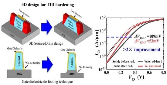
3.3. TID Hardening Result

The proposed rad-hard design improves the TID tolerance of the device by reducing the sensitivity of it to TID charges. The transfer characteristics of the 14 nm node SOI FinFETs with and without rad-hard design are shown in Figure 4. The rad-hard design can effectively reduce the TID-induced ΔVTSAT (defined as a constant current threshold voltage and extracted at IDS = 1 μA/μm) from 109 mV to 53 mV (factor >2×). It is also worth noting that the rad-hard design does not degrade device performance. The simulated SOI FinFETs’ electrical parameters are listed in Table 3. It is worth noting that the 3D design features a 14 mV/dec improved SS, together with a 15% higher ION compared to conventional SOI FinFETs, suggesting that TID hardening can be achieved without sacrificing device performance.

3.4. Analysis and Discussion

3.4.1. TID Effect’s Mechanism in SOI FinFETs

The most significant impact of the TID effect is the ΔVTSAT [9,10,11], which is governed by two factors: the trapped charge density and its coupling to the sub-threshold current path. The first factor is proportional to the electric field perpendicular to the channel/BOX interface [38]. The second factor is determined by the distance between the current path and the BOX (where the trapped charge exists). Therefore, the TID’s impact can be effectively suppressed by reducing the electric field in the BOX together with shifting the leakage current towards the fin top.
In FinFETs with a realistic tapered fin, the sub-threshold current’s distribution is controlled by the local gate electrostatic control as well as the drain fringing field [29]. In an SOI FinFET with a 150 nm LG (Figure 5a), the drain fringing field is relatively weak, resulting in an almost uniform sub-threshold energy barrier profile in the channel (Figure 5b). The current density is higher near the fin top, which is caused by the extra top gate control (Figure 5c). Therefore, its coupling effect to the TID-induced trapped charge is reasonably weak. Meanwhile, the low drain fringing field leads to a moderate off-state electric field in the BOX (Figure 5d) and a relatively low charge-trapping rate, further suppressing the transistor’s sensitivity to the TID irradiation.
However, the TID’s impact becomes more critical as the transistors scale down. This is dominated by the drastically increased drain fringing field in ultra-scaled devices. In a tapered fin, the local TSi near the fin bottom is larger than that near the fin top (Figure 2c) and thus results in a reduced local gate electrostatic control. This phenomenon has been thoroughly discussed in [30,39]. Therefore, the drain fringing field has a stronger impact on the virtual cathode (analogous to the DIBL effect in planar FETs), forming a localized virtual cathode (Figure 6a). Instead of forming an almost uniform current distribution in the SOI FinFET with a 150 nm LG (Figure 5c), a localized sub-threshold current path is formed near the fin bottom (Figure 6b). The reduced distance between the current path and the BOX results in an extensively stronger coupling, increasing the TID’s impact on device performance. TCAD simulations show that the device becomes significantly more sensitive to the TID irradiation. The ΔVTSAT induced by a 4 × 1011 cm−2 TID charge increases by 48 mV (from 61 mV to 109 mV, 1.8×) as the LG scales (Figure 7). This trend is consistent with experimental results [22], adding credibility to the analysis. In addition, the higher electric field in the BOX (Figure 6b) also increases the charge trapping rate [38], further reducing SOI FinFET’s TID tolerance. Therefore, it is of great significance to develop a TID hardening technique for ultra-scaled SOI FinFETs.

3.4.2. TID Hardening Methodology

Physical interpretation shows that the relatively low TID tolerance in conventional 14 nm node SOI FinFET is strongly influenced by the localization of the sub-threshold current path. Therefore, the TID hardening design focuses on suppressing the drain fringing field and improving the gate electrostatic control, especially near the fin bottom where the leakage path occurs. This can be effectively achieved by combining the 3D S/D module and the gate dielectric de-footing process (Figure 8a). The former suppresses the fin bottom dopant encroachment and reduces the local drain fringing field [29], while the latter enhances the local gate electrostatic control. Both optimizations contribute to increasing the barrier energy near the fin bottom, resulting in a virtual cathode shifted towards the fin top (Figure 8b). The sub-threshold current path modulation (Figure 8c) suppresses the coupling effect to the trapped charge in the BOX and therefore reduces the ΔVTSAT by >2×, as shown in Figure 4.
Moreover, the electric field distribution in the BOX of the rad-hard SOI FinFET is also investigated (Figure 8c). The rad-hard design reduces the drain fringing field near the fin bottom and thus decreases the electric field in the BOX, especially under the channel region. This suppresses the charge accumulation during irradiation, further improving the TID tolerance of the 14 nm node SOI FinFET.

4. Conclusions

In this work, an innovative TID hardening design, combining a 3D S/D doping technique and a gate dielectric de-footing process, is proposed for 14 nm node SOI FinFETs, and the optimization methodology is well established. The strong coupling between the localized leakage path near the fin bottom and the radiation-induced trapped charge in the BOX is identified as the dominating factor in the increasingly critical TID effect in aggressively scaled SOI FinFETs. By improving the gate electrostatic control close to the fin bottom, the rad-hard design can effectively shift the leakage path toward the fin top. As a result, the ΔVTSAT is effectively reduced by >2× from 109 mV to 53 mV without degrading device performance. Moreover, the TID charge capture rate is also reduced by suppressing the electric field in the BOX, further enhancing the device’s robustness. The optimization methodology in this work can provide guidance for irradiation resistance improvement in advanced devices, paving the way for their application in future deep space exploration missions.

Author Contributions

Data curation, P.L., C.Y. and Y.L.; Formal analysis, P.L. and C.Y.; Investigation, P.L., C.Y. and Y.L.; Methodology, P.L., C.Y. and Y.L.; Project administration, P.L., B.L. and Z.H.; Supervision, B.L. and Z.H.; Visualization, C.Y. and Y.L.; Writing—original draft, P.L., C.Y. and Y.L.; Writing—review & editing, P.L., C.Y. and Y.L. All authors have read and agreed to the published version of the manuscript.

Funding

This research was funded by National Natural Science Foundation of China grant number 6187032253.

Institutional Review Board Statement

Not applicable.

Informed Consent Statement

Not applicable.

Acknowledgments

The authors would like to thank Qingzhu Zhang in IMECAS for supplying SOI FinFET TEM images.

Conflicts of Interest

The authors declare no conflict of interest.

References

  1. Jan, C.-H.; Bhattacharya, U.; Brain, R.; Choi, S.-J.; Curello, G.; Gupta, G.; Hafez, W.; Jang, M.; Kang, M.; Komeyli, K.; et al. A 22nm SoC platform technology featuring 3-D tri-gate and high-k/metal gate, optimized for ultra low power, high performance and high density SoC applications. In Proceedings of the 2012 International Electron Devices Meeting, San Francisco, CA, USA, 10–13 December 2012; pp. 3.1.1–3.1.4. [Google Scholar] [CrossRef]
  2. Natarajan, S.; Agostinelli, M.; Akbar, S.; Bost, M.; Bowonder, A.; Chikarmane, V.; Chouksey, S.; Dasgupta, A.; Fischer, K.; Fu, Q.; et al. A 14nm logic technology featuring 2nd-generation FinFET, air-gapped interconnects, self-aligned double patterning and a 0.0588 m2 SRAM cell size. In Proceedings of the 2014 IEEE International Electron Devices Meeting, San Francisco, CA, USA, 15–17 December 2014; pp. 3.7.1–3.7.3. [Google Scholar] [CrossRef]
  3. Auth, C.; Aliyarukunju, A.; Asoro, M.; Bergstrom, D.; Bhagwat, V.; Birdsall, J.; Bisnik, N.; Buehler, M.; Chikarmane, V.; Ding, G.; et al. A 10nm high performance and low-power CMOS technology featuring 3rd generation FinFET transistors, Self-Aligned Quad Patterning, contact over active gate and cobalt local interconnects. In Proceedings of the 2017 IEEE International Electron Devices Meeting (IEDM), San Francisco, CA, USA, 2–6 December 2017; pp. 29.1.1–29.1.4. [Google Scholar] [CrossRef]
  4. Hashemi, P.; Balakrishnan, K.; Majumdar, A.; Khakifirooz, A.; Kim, W.; Baraskar, A.; Yang, L.A.; Chan, K.; Engelmann, S.U.; Ott, J.A.; et al. Strained Si1xGex-on-insulator PMOS FinFETs with excellent sub-threshold leakage, extremely-high short-channel performance and source injection velocity for 10nm node and beyond. In Proceedings of the 2014 Symposium on VLSI Technology (VLSI-Technology): Digest of Technical Papers, Honolulu, HI, USA, 9–12 June 2014; pp. 1–2. [Google Scholar] [CrossRef]
  5. Liu, J.; Mukhopadhyay, S.; Kundu, A.; Chen, S.; Wang, H.; Huang, D.; Lee, J.; Wang, M.; Lu, R.; Lin, S.; et al. A Reliability Enhanced 5nm CMOS Technology Featuring 5th Generation FinFET with Fully-Developed EUV and High Mobility Channel for Mobile SoC and High Performance Computing Application. In Proceedings of the 2020 IEEE International Electron Devices Meeting (IEDM), San Francisco, CA, USA, 12–18 December 2020; pp. 9.2.1–9.2.4. [Google Scholar] [CrossRef]
  6. Yonghong, L.; Chaohui, H.; Fazhan, Z.; Tianlei, G.; Gang, L.; Zhengsheng, H.; Jie, L.; Gang, G. Experimental study on heavy ion single event effects in SOI SRAMs. Nucl. Instrum. Methods Phys. Res. Sect. B Beam Interact. Mater. Atoms 2009, 267, 83–86. [Google Scholar] [CrossRef]
  7. Li, G.; An, X.; Ren, Z.; Wang, J.; Huang, R. Investigation on Impact of Fin Width on Single-Event-Transient in Bulk and SOI FinFETs. In Proceedings of the 2018 14th IEEE International Conference on Solid-State and Integrated Circuit Technology (ICSICT), Qingdao, China, 31 October–3 November 2018; pp. 1–3. [Google Scholar] [CrossRef]
  8. Hughes, H.; McMarr, P.; Alles, M.; Zhang, E.; Arutt, C.; Doris, B.; Liu, D.; Southwick, R.; Oldiges, P. Total Ionizing Dose Radiation Effects on 14 nm FinFET and SOI UTBB Technologies. In Proceedings of the 2015 IEEE Radiation Effects Data Workshop (REDW), Boston, MA, USA, 13–17 July 2015; pp. 1–6. [Google Scholar] [CrossRef] [Green Version]
  9. Tan, F.; Huang, R.; An, X.; Wu, W.; Feng, H.; Huang, L.; Fan, J.; Zhang, X.; Wang, Y. Total ionizing dose (TID) effect and single event effect (SEE) in quasi-SOI nMOSFETs. Semicond. Sci. Technol. 2013, 29, 015010. [Google Scholar] [CrossRef]
  10. Rezzak, N.; Zhang, E.X.; Ball, D.R.; Alles, M.L.; Loveless, T.D.; Schrimpf, R.D.; Rodbell, K. Total-ionizing-dose radiation response of 32 nm partially and 45 nm fully-depleted SOI devices. In Proceedings of the 2012 IEEE International SOI Conference (SOI), Napa, CA, USA, 1–4 October 2012; pp. 1–2. [Google Scholar] [CrossRef]
  11. Domae, Y.; Komatsubara, H.; Shindou, H.; Makihara, A.; Kuboyama, S.; Ida, J. Improvement of the tolerance to total ionizing dose in SOI CMOS. In Proceedings of the 2008 IEEE International SOI Conference, New Paltz, NY, USA, 6–9 October 2008; pp. 135–136. [Google Scholar]
  12. Li, B.; Huang, Y.; Wu, J.; Zhang, Q.; Yang, L.; Wan, F.; Luo, J.; Han, Z.; Yin, H. Constant voltage stress characterization of nFinFET transistor during total ionizing dose experiment. Microelectron. Reliab. 2018, 88–90, 969–973. [Google Scholar] [CrossRef]
  13. Ren, Z.; An, X.; Li, G.; Chen, G.; Li, M.; Yu, G.; Guo, Q.; Zhang, X.; Huang, R. TID Response of Bulk Si PMOS FinFETs: Bias, Fin Width, and Orientation Dependence. IEEE Trans. Nucl. Sci. 2020, 67, 1320–1325. [Google Scholar] [CrossRef]
  14. Moon, J.-B.; Moon, D.-I.; Choi, Y.-K. Influence of Total Ionizing Dose on Sub-100 nm Gate-All-Around MOSFETs. IEEE Trans. Nucl. Sci. 2014, 61, 1420–1425. [Google Scholar] [CrossRef]
  15. Huang, Y.; Li, B.; Zhao, X.; Zheng, Z.; Gao, J.; Zhang, G.; Li, B.; Zhang, G.; Tang, K.; Han, Z.; et al. An Effective Method to Compensate Total Ionizing Dose-Induced Degradation on Double-SOI Structure. IEEE Trans. Nucl. Sci. 2018, 65, 1532–1539. [Google Scholar] [CrossRef]
  16. Gaillardin, M.; Martinez, M.; Paillet, P.; Raine, M.; Andrieu, F.; Faynot, O.; Thomas, O. Total Ionizing Dose Effects Mitigation Strategy for Nanoscaled FDSOI Technologies. IEEE Trans. Nucl. Sci. 2014, 61, 3023–3029. [Google Scholar] [CrossRef]
  17. Roh, Y.T.; Lee, H.C. Layout Modification of a PD-SOI n-MOSFET for Total Ionizing Dose Effect Hardening. IEEE Trans. Electron Devices 2018, 66, 308–315. [Google Scholar] [CrossRef]
  18. Liu, C.; Zhu, H.; Xie, X.; Hu, Z.; Bi, D.; Zhang, Z.; Zou, S. Investigation of Radiation Hardening by Back-Channel Adjustment in PDSOI MOSFETs. IEEE Trans. Nucl. Sci. 2021, 68, 2609–2615. [Google Scholar] [CrossRef]
  19. Peng, C.; Hu, Z.; En, Y.; Chen, Y.; Lei, Z.; Zhang, Z.; Zhang, Z.; Li, B. Radiation Hardening by the Modification of Shallow Trench Isolation Process in Partially Depleted SOI MOSFETs. IEEE Trans. Nucl. Sci. 2018, 65, 877–883. [Google Scholar] [CrossRef]
  20. Li, B.; Wu, J.; Gao, J.; Kuang, Y.; Li, J.; Zhao, X.; Zhao, K.; Han, Z.; Luo, J. The total ionizing dose response of a DSOI 4Kb SRAM. Microelectron. Reliab. 2017, 76–77, 714–718. [Google Scholar] [CrossRef]
  21. Li, B.; Zhao, K.; Wu, J.; Zhao, X.; Su, J.; Gao, J.; Gao, C.; Luo, J. Electromagnetic susceptibility characterization of double SOI device. Microelectron. Reliab. 2016, 64, 168–171. [Google Scholar] [CrossRef]
  22. Chatterjee, I.; Zhang, E.X.; Bhuva, B.L.; Reed, R.A.; Alles, M.L.; Mahatme, N.N.; Ball, D.R.; Schrimpf, R.D.; Fleetwood, D.M.; Linten, D.; et al. Geometry Dependence of Total-Dose Effects in Bulk FinFETs. IEEE Trans. Nucl. Sci. 2014, 61, 2951–2958. [Google Scholar] [CrossRef]
  23. Duan, G.X.; Zhang, C.X.; Zhang, E.X.; Hachtel, J.; Fleetwood, D.M.; Schrimpf, R.D.; Reed, R.A.; Alles, M.L.; Pantelides, S.T.; Bersuker, G.; et al. Bias Dependence of Total Ionizing Dose Effects in SiGe-MOS FinFETs. IEEE Trans. Nucl. Sci. 2014, 61, 2834–2838. [Google Scholar] [CrossRef]
  24. Riffaud, J.; Gaillardin, M.; Marcandella, C.; Martinez, M.; Paillet, P.; Duhamel, O.; Lagutere, T.; Raine, M.; Richard, N.; Andrieu, F.; et al. Investigations on the Geometry Effects and Bias Configuration on the TID Response of nMOS SOI Tri-Gate Nanowire Field-Effect Transistors. IEEE Trans. Nucl. Sci. 2017, 65, 39–45. [Google Scholar] [CrossRef]
  25. Zhang, Q.; Yin, H.; Luo, J.; Yang, H.; Meng, L.; Li, Y.; Wu, Z.; Zhang, Y.; Zhang, Y.; Qin, C.; et al. FOI FinFET with ultra-low parasitic resistance enabled by fully metallic source and drain formation on isolated bulk-fin. In Proceedings of the 2016 IEEE International Electron Devices Meeting (IEDM), San Francisco, CA, USA, 3–7 December 2016; pp. 17.3.1–17.3.4. [Google Scholar] [CrossRef]
  26. Li, B.; Huang, Y.-B.; Yang, L.; Zhang, Q.-Z.; Zheng, Z.-S.; Zhu, H.-P.; Bu, J.-H.; Yin, H.-X.; Luo, J.-J.; Han, Z.-S.; et al. Process variation dependence of total ionizing dose effects in bulk nFinFETs. Microelectron. Reliab. 2018, 88–90, 946–951. [Google Scholar] [CrossRef]
  27. Mochizuki, S.; Colombeau, B.; Yu, L.; Dube, A.; Choi, S.; Stolfi, M.; Bi, Z.; Chang, F.; Conti, R.A.; Liu, P.; et al. Advanced Arsenic Doped Epitaxial Growth for Source Drain Extension Formation in Scaled FinFET Devices. In Proceedings of the 2018 IEEE International Electron Devices Meeting (IEDM), San Francisco, CA, USA, 1–5 December 2018; pp. 35.2.1–35.2.4. [Google Scholar] [CrossRef]
  28. Badran, M.S.; Issa, H.H.; Eisa, S.M.; Ragai, H. Low Leakage Current Symmetrical Dual-k 7 nm Trigate Bulk Underlap FinFET for Ultra Low Power Applications. IEEE Access 2019, 7, 17256–17262. [Google Scholar] [CrossRef]
  29. Yoon, J.-S.; Jeong, J.; Lee, S.; Baek, R.-H. Sensitivity of Source/Drain Critical Dimension Variations for Sub-5-nm Node Fin and Nanosheet FETs. IEEE Trans. Electron Devices 2020, 67, 258–262. [Google Scholar] [CrossRef]
  30. Liang, X.; Taur, Y. A 2-D Analytical Solution for SCEs in DG MOSFETs. IEEE Trans. Electron Devices 2004, 51, 1385–1391. [Google Scholar] [CrossRef]
  31. Seo, K.-I.; Haran, B.; Gupta, D.; Guo, D.; Standaert, T.; Xie, R.; Shang, H.; Alptekin, E.; Bae, D.-I.; Bae, G.; et al. A 10nm platform technology for low power and high performance application featuring FINFET devices with multi workfunction gate stack on bulk and SOI. In Proceedings of the 2014 Symposium on VLSI Technology (VLSI-Technology): Digest of Technical Papers, Honolulu, HI, USA, 9–12 June 2014; pp. 1–2. [Google Scholar] [CrossRef]
  32. Synopsys Inc. Sentaurus User’s Manual; Synopsys: Mountain View, CA, USA, 2018. [Google Scholar]
  33. Granzner, R.; Polyakov, V.; Schwierz, F.; Kittler, M.; Luyken, R.; Rösner, W.; Städele, M. Simulation of nanoscale MOSFETs using modified drift-diffusion and hydrodynamic models and comparison with Monte Carlo results. Microelectron. Eng. 2006, 83, 241–246. [Google Scholar] [CrossRef]
  34. Tsutsui, G.; Saitoh, M.; Saraya, T.; Nagumo, T.; Hiramoto, T. Mobility enhancement due to volume inversion in [110]-oriented ultra-thin body double-gate nMOSFETs with body thickness less than 5 nm. In Proceedings of the IEEE InternationalElectron Devices Meeting, 2005. IEDM Technical Digest, Washington, DC, USA, 5 December 2005; pp. 729–732. [Google Scholar] [CrossRef]
  35. Simoen, E.; Gaillardin, M.; Paillet, P.; Reed, R.A.; Schrimpf, R.; Alles, M.L.; El-Mamouni, F.; Fleetwood, D.M.; Griffoni, A.; Claeys, C. Radiation Effects in Advanced Multiple Gate and Silicon-on-Insulator Transistors. IEEE Trans. Nucl. Sci. 2013, 60, 1970–1991. [Google Scholar] [CrossRef]
  36. Haeffner, T.D.; Reed, R.A.; Schrimpf, R.D.; Fleetwood, D.M.; Keller, R.F.; Jiang, R.; Sierawski, B.D.; McCurdy, M.W.; Zhang, E.X.; Mohammed, R.W.; et al. Comparison of Total-Ionizing-Dose Effects in Bulk and SOI FinFETs at 90 and 295 K. IEEE Trans. Nucl. Sci. 2019, 66, 911–917. [Google Scholar] [CrossRef]
  37. Shu, L.; Wang, L.; Zhao, K.; Zhou, X.; Zhao, Y.-F.; Galloway, K.F.; Sui, C.-L.; Liu, C.-M.; Cao, W.-Y.; Chen, W.-P.; et al. TID-Induced OFF-State Leakage Current in Partially Radiation-Hardened SOI LDMOS. IEEE Trans. Nucl. Sci. 2020, 67, 1133–1138. [Google Scholar] [CrossRef]
  38. Alles, M.L.; Hughes, H.L.; Ball, D.R.; McMarr, P.J.; Schrimpf, R.D. Total-Ionizing-Dose Response of Narrow, Long Channel 45 nm PDSOI Transistors. IEEE Trans. Nucl. Sci. 2014, 61, 2945–2950. [Google Scholar] [CrossRef]
  39. Lu, P.; Colombeau, B.; Hung, S.; Li, W.; Duan, X.; Li, Y.; Bazizi, E.M.; Natarajan, S.; Woo, J.C.S. Source/Drain Extension Doping Engineering for Variability Suppression and Performance Enhancement in 3-nm Node FinFETs. IEEE Trans. Electron Devices 2021, 68, 1352–1357. [Google Scholar] [CrossRef]
Figure 1. Comparison between a conventional SOI FinFET and the proposed 3D design. (a) A 3D schematic of a conventional SOI FinFET with a vertically uniform S/D, (b) a 3D schematic of the SOI FinFET with the proposed 3D S/D design, (c) the fin cross-section in a conventional SOI FinFET and (d) the fin cross-section in with an optimized gate dielectric.
Eng 02 00039 g001
Figure 2. Simulated SOI FinFET structures for TID hardening evaluation. (a,b) 3D schematics of a conventional design and the proposed rad-hard design, respectively; (c,d) fin cross-sections in a conventional device and the rad-hard device, respectively.
Eng 02 00039 g002
Figure 3. The 14 nm node FinFET process results for physical parameter extraction. (a) The 3D S/D’s TEM and (b) the fin geometry fabricated by IMECAS [25]. The extracted physical parameters are listed in Table 2.
Eng 02 00039 g003
Figure 4. Comparison of the (a) log scale and (b) linear scale transfer characteristics’ drift caused by the total dose radiation in SOI n-FinFETs with and without reinforcement.
Eng 02 00039 g004
Figure 5. Simulation results of a long channel (LG = 150 nm) SOI n-FinFET. (a) Schematics of the simulated device, (b) the potential energy distribution in channel region, (c) the sub-threshold current distribution in the tapered fin and (d) the distribution of the electric field in the BOX perpendicular to the channel/BOX interface.
Eng 02 00039 g005
Figure 6. Simulation results of the 14 nm node SOI n-FinFET without TID hardening. (a) The potential energy distribution in channel region, (b) the sub-threshold current distribution in the tapered fin and (c) the distribution of the electric field in the BOX perpendicular to the channel/BOX interface.
Eng 02 00039 g006
Figure 7. Comparison of the (a) log scale and (b) linear scale transfer characteristics’ drift caused by the total dose radiation in long channel (LG = 150 nm) and 14 nm node (LG = 20 nm) SOI n-FinFETs.
Eng 02 00039 g007
Figure 8. Simulation results of the 14 nm node SOI n-FinFET with the TID hardening design. (a) The potential energy distribution in channel region, (b) the sub-threshold current distribution in the tapered fin and (c) the distribution of the electric field in the BOX perpendicular to the channel/BOX interface.
Eng 02 00039 g008aEng 02 00039 g008b
Table 1. Reported TID hardening methodology based on SOI technology and their compatibility with SOI FinFETs.
ReferenceTID Hardening MethodologySOI FinFET
Compatible
Y. Huang et al. [15]Double SOIN
M. Gaillardin et al. [16]Ground plane implantation under the BOXN
Y. T. Roh et al. [17]Dummy gate-assisted SOIN
C. Liu et al. [18]Back-channel adjustmentN
C. Peng et al. [19]STI oxide nitridationN
This work3D S/D & gate dielectric optimizationY
Table 2. Physical parameters used in 14 nm node SOI FinFET simulations.
Physical ParametersConventional DesignRad-Hard Design
Fin top width (nm)10
Fin height (nm)25
Fin pitch (nm)40
Taper angle (°)79
Channel length (nm)20
Fin top spacer length (nm)10
S/D doping concentration (cm−3)2 × 10²⁰
Channel doping concentration (cm−3)1016
Junction doping diffusion gradient (nm/dec)5
Fin top EOT (nm)1.0
Fin bottom spacer length (nm)1030
Fin bottom EOT (nm)1.21.0
Oxide footingYesNo
Table 3. Simulated electrical characteristics of 14 nm node SOI FinFETs with various designs and radiation conditions.
Electrical CharacteristicsConventional
Design before
Radiation
Conventional
Design after
Radiation
3D Design
before Radiation
3D Design
after Radiation
Threshold Voltage (V)0.3290.2200.2580.205
On-state Current (A/μm)5.80 × 10−46.85 × 10−46.71 × 10−47.17 × 10−4
Off-state Current (A/μm)1.0 × 10−103.5 × 10−91.0 × 10−108.2 × 10⁻¹⁰
Sub-threshold Swing(mV/dec)79.085.964.967.4
Transconductance (mS/μm)1.962.131.511.56
Publisher’s Note: MDPI stays neutral with regard to jurisdictional claims in published maps and institutional affiliations.

