Review

Recent Progress in Short and Mid-Infrared Single-Photon Generation: A Review

by
Arianna Elefante
,
Stefano Dello Russo
,
Fabrizio Sgobba
,
Luigi Santamaria Amato
,
Deborah Katia Pallotti
,
Daniele Dequal
and
Mario Siciliani de Cumis
*
Italian Space Agency (ASI), Centro di Geodesia Spaziale ‘Giuseppe Colombo’, Località Terlecchia, 75100 Matera, Italy
*
Author to whom correspondence should be addressed.
Optics 2023, 4(1), 13-38; https://doi.org/10.3390/opt4010003
Submission received: 25 November 2022 / Revised: 20 December 2022 / Accepted: 10 January 2023 / Published: 12 January 2023

Abstract

:
The generation of single photons in the mid-infrared spectral region is attracting the interest of scientific and technological research, motivated by the potential improvements that many important and emerging applications, such as quantum sensing, metrology and communication, could benefit from. This review reports the progress in short and mid-infrared single photon generation, focusing on probabilistic sources based on the two non-linear processes of spontaneous parametric downconversion (SPDC) and four wave mixing (FWM). On one hand, numerical simulations of mid-infrared SPDC are described as a powerful tool to assist and guide the experimental realization, along with the implementation and engineering of novel non-linear materials. On the other hand, the advantages offered by FWM in silicon waveguides in terms of integration, miniaturization and manufacturability are presented, providing an optimal technology for integrated quantum applications.

1. Introduction

Nowadays, there is a rapidly expanding research focus on developing new quantum optical technologies which are opening the way to novel applications in quantum sensing, metrology, simulation, computing and communication. The common requirement at the heart of all these applications is the availability of a quantum photonic platform for the generation, manipulation and measurement of single photons and correlated photon pairs. Single photons are essential for quantum sensing [1] to perform absorption measurement in the few-photon regime, in quantum metrology [2] to allow the subshot-noise phase estimation, as well as in imaging [3]. Entangled photon pairs are becoming key components in quantum information processing [4] including quantum key distribution [5], connecting quantum nodes [6], tests of the Bell inequality [7], and generation of certified random numbers [8].
A large variety of quantum systems have been developed so far to make possible the implementation of the mentioned applications, ranging from trapped atoms, defects in solid state, superconductor structures as well as nonlinear materials to generate correlated photon pairs. The generation of photon pairs by using nonlinear optical processes has been widely investigated both in the visible range, achieving emission with a wide bandwidth [9] and high efficiency [10], and in the near-IR, especially at the telecom band at 1550 nm for applications such as qubits in quantum network or quantum communication at long distance [11] by using a bright photon-pair source.
A further challenging step that is attracting research and technological interest, is the extension of quantum systems to longer wavelengths, where quantum applications could fully harness their potential. The interesting wavelength range includes the short-infrared [1.5–3] µm, the mid-infrared [3–8] µm and the long-infrared [8–15] µm. The strong absorption bands of most gases in the mid-infrared (MIR) range promote and enhance gas sensing [12] and environmental monitoring applications [13] at these wavelengths, as well as quantum LIDAR [14]. Quantum infrared thermal imaging benefits from the emission of MIR light by room temperature objects [15]. Medical imaging [16,17,18] at ultra-low light levels would be realized. Among all the applications, the main driving force pushing the research on MIR single photon sources is the field of quantum information and communications. In this context, quantum key distribution (QKD) is at the heart of cryptography as a powerful tool to distribute a secrete key between two parties, with unconditional security of communication guaranteed by the quantum laws of physics. Extending the QKD to the MIR region, with respect to the NIR systems already implemented both in optical fiber or free-space links, could result in a higher bit rate and higher maximum distance achieved [19], thanks to several advantages inherited by the MIR operation. For free space secure communication [20], the atmospheric transparency window between 3 and 5 μm, as well as the one at 10 μm [21], presents a Rayleigh scattering cross-section well reduced compared to the NIR region, which is particularly helpful in the presence of fog or haze [22,23]. For daylight communication, the background radiation from the sun causes a binding effect, which in the MIR range is up to three times lower compared to the NIR 1550 nm wavelength. For fiber-based communication, the extension to MIR can increase the communication bandwidth [24].
The realization of all these applications requires, as the first step, the development of well performing single photon and photon-pair sources in the MIR wavelength range, as well as of single photons detectors [25]. A bridge between the potential of the quantum applications and the existing immature quantum MIR technologies would make accessible the benefits of the MIR range for quantum applications which have not been fully exploited yet due to technological limitations. The photon sources must match the requirements of device miniaturization and compactness required by most quantum photonics applications, where the capability to integrate the source and the detector on a single chip using nanophotonics fabrication is crucial for large-scale implementation of quantum-enhanced technology. Integrated optics could provide bright sources due to strong confinement and long interaction length, high speed switching enabled by low required voltage, compactness and robustness [26].
This review is focused on the state of art of single photon and photon pair sources in the challenging MIR range. In Section 2 the basic working principle of the probabilistic sources based on the non-linear processes of spontaneous parametric downconversion (SPDC) and four wave mixing (FWM) will be introduced, followed by an outlook on the main features used to characterize these sources in Section 3. Section 4 is focused on the SPDC process for the generation of MIR photons: the helpful contribution offered by numerical simulations on SPDC processes based on novel non-linear materials as well as experimental implementations of MIR SPDC will be presented. In Section 5 the most promising results concerning the generation of MIR heralded single photons through FWM will be discussed, with a particular emphasis on the possibility of integration derived by the exploitation of silicon waveguides.

2. Probabilistic Sources

An ideal on demand photon source producing a single photon in a known mode every time it is called for is not achievable because of inevitable system losses and non-zero multiphoton rates [26]. There are three main approaches that can be implemented to approximate the ideal behavior of a single photon source: strongly attenuated laser light [27,28], deterministic sources based on isolated single quantum systems that can only emit one photon at a time [29], or probabilistic sources [26]. Probabilistic sources are based on photons created in pairs through mainly two mechanisms, both based on the laser excitation of a nonlinear optical material: spontaneous parametric downconversion in bulk crystals and waveguides and four wave mixing in optical fibers. The powerful peculiarity of these photon pair sources is the capability to be implemented as a “heralded” single photon source, where the detection of one photon in one arm heralds the existence of a photon in the other arm. This feature represents the pillar for a wide range of experiments, from tests of fundamental physics [7,30] to metrology [2], to entanglement-enhanced applications [31].
The non-deterministic nature of such single photon sources is a limitation that could prevent them to simultaneously reach a high probability of producing a photon and a high single photon fidelity [32]. Nevertheless, the probabilistic nature of SPDC sources can be bypassed with the implementation of proper schemes, which allow approximation of them to nearly deterministic photon sources with high production rates and photon purity. These approaches are based on photon source multiplexing [26]: array of low-probability, but high-fidelity photon pair sources are used, creating a system with the probability that at least one source generates a photon pair tending to unity, as the number of the sources increase, maintaining at the same time high single-photon fidelity. Several schemes can be adopted, based on temporal, spatial or frequency multiplexing. The general structure of a multiplexed source consists of multiple pair sources pumped simultaneously, each with its own heralding detector. If one heralding detector fires, the corresponding partner photon is directed to the output. If multiple detectors fire, just one of the partner photons is directed to the output, removing the other photons to not deteriorate the single-photon state.

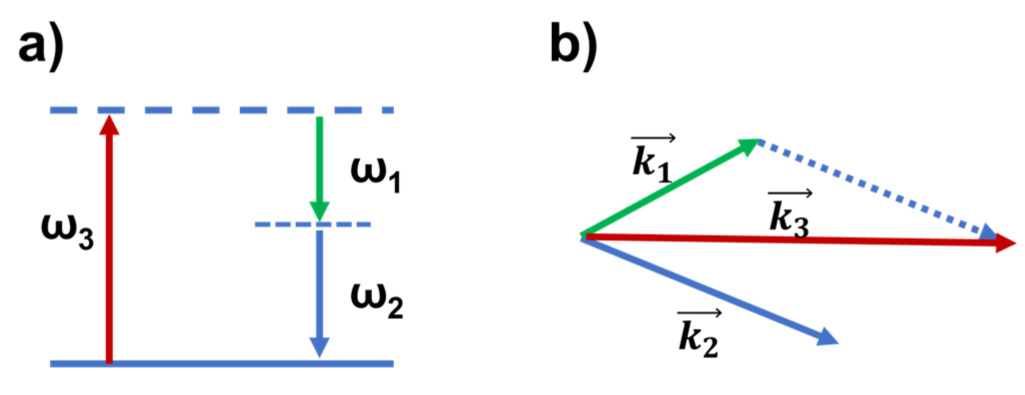
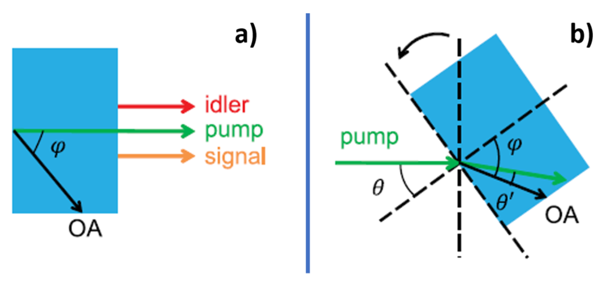
2.1. Parametric Downconversion

SPDC is at the heart of many quantum optics experiments [33], having demonstrated the capability to generate high-quality single photons as well as entangled photons used for quantum teleportation, cryptography computation and metrology applications.
SPDC is a non-linear optical process where a single pump photon, passing through a non-linear optical material, spontaneously decays into two photons of lower energy, the signal and idler photons. It involves the use of a pump laser illuminating a material with a Χ(2) optical non linearity, creating two photons under the constraints of momentum and energy conservation. Figure 1 shows the representation of energy (Figure 1a) and momentum (Figure 1b) conservation for a SPDC process where photon γ3 at energy ω3 splits into two photons γ1 and γ2 at energies ω1 and ω2. Usually, SPDC processes can be classified by the polarizations of the pump, signal and idler photons: in type-0 the signal and idler photons have the same polarization with each other and with the pump photon; in type-1 SPDC the signal and idler photons share the same polarization to each other, however they are orthogonal to the pump polarization; in type-2 the signal and idler photons present perpendicular polarizations.
In order to be efficient, the SPDC process requires energy and momentum conservation, expressed by the so-called phase matching conditions which determine the possible energy and wavevector relations between the two downconverted photons.
ωp = ωs + ωi
k p = k s + k i     2 π n λ p ,   T λ p = 2 π   n λ s ,   T λ s + n λ i ,   T λ i
where kj and ωj (j = p, s, i) are the wave numbers and angular frequencies for the pump, signal and idler photons, n(λ, T) is the refractive index of the material that depends on the wavelength λ of the optical signal and on the temperature T of the non-linear crystal.
The natural dispersion of the non-linear crystal makes it difficult to satisfy the momentum conservation. Techniques such as quasi-phase-matching (QPM) via periodic poling of the nonlinear crystals enable compensation of the wave vector mismatch by appending an additional wave vector kg = 2π/Λ of the poled grating, where Λ is the period of poling, which represents an imposed periodicity on the nonlinear coefficient of the nonlinear crystal. The poling technology consists in a lithographic electrode mask implemented across the crystal, with the application of an electric field poling of periodic domains of alternating polarity. The poling counteracts the dispersion between the interacting wavelengths, making it possible to satisfy Equation (2) thanks to the addition of the poling term that is inversely proportional to Λ:
  k p = k s + k i ± 2 π Λ
When the poling period is known, it is possible to calculate the spectrum of the SPDC generated photon pairs depending on the crystal temperature.

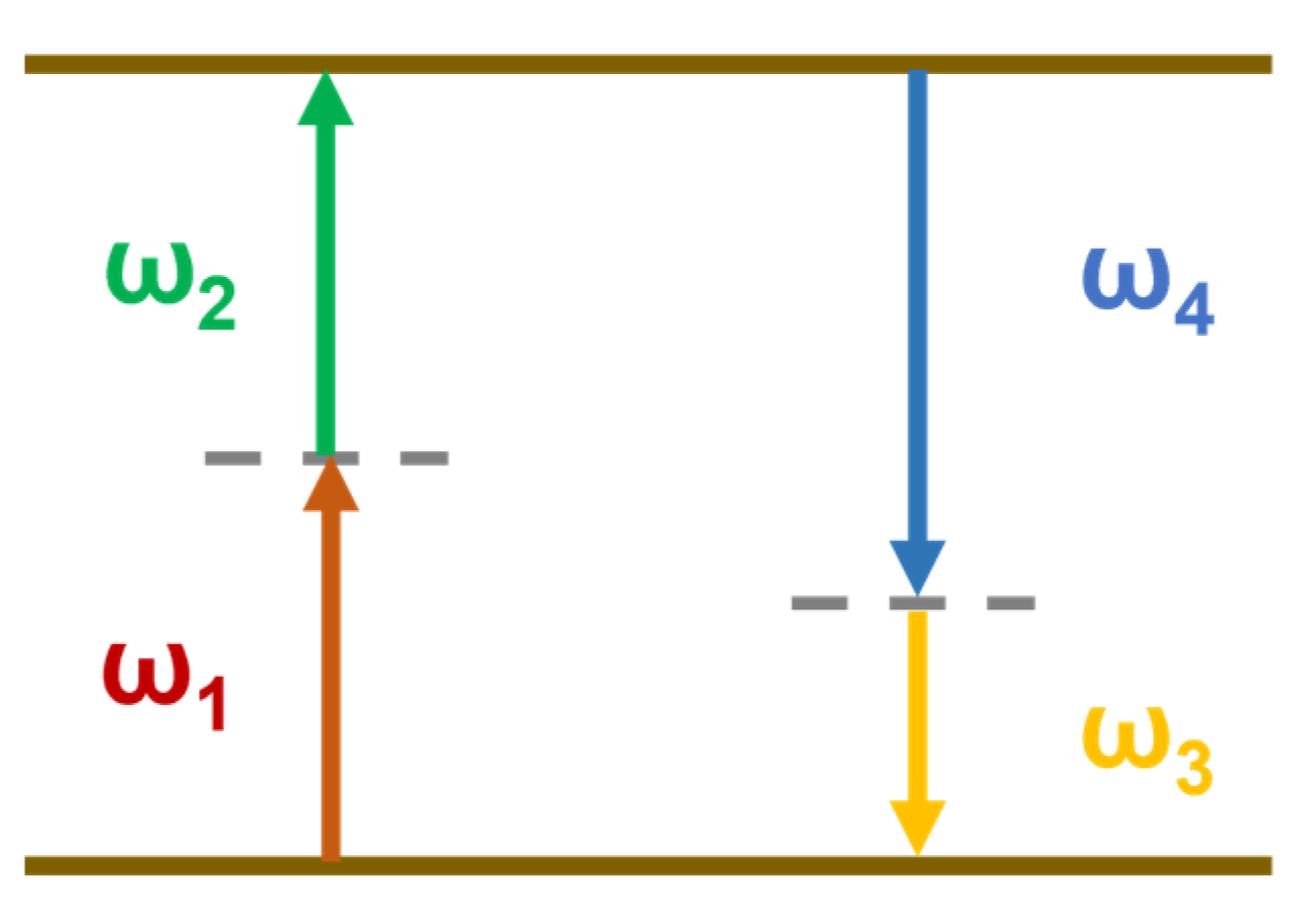
2.2. Four Wave Mixing

Four wave mixing is a third-order electric susceptibility Χ(3) non linear process in which two pump photons with angular frequency ωp1 and ωp2 are converted into two correlated photons which are detuned in frequency from the pump by ±Ω, as shown in the schematic in Figure 2. It mainly occurs in centrosymmetric materials not allowing the Χ(2) non linearity.
As SPDC, FWM conserves energy and momentum and to have an efficient process the phase-matching condition must be satisfied, with a total wave-vector mismatch Δ k is equal to zero.
ωp1 + ωp2 = ωs + ωi
kp1 + kp1 = ks + ki
FWM have been widely exploited to generate correlated photon pairs using single-mode optical fibers, photonic crystal fibers, birefringent single-mode fiber and most recently Silicon-On-Insulator waveguides (SOI) [34]. In particular, FWM in SOI waveguides will be discussed in the next section being a promising structure for high-density integration of optical circuits, showing advantages with respect to standard optical fibers. The crystalline nature of the silicon material leads to significantly lesser broadening of the Raman vibrational mode compared to the one obtained in standard optical fibers made of glass [35]. This would result in a reduction of the spontaneous Raman scattering, which is one of the fundamental sources of noise when generating photons with FWM. Moreover, the large susceptibility of nanoscale silicon waveguides leads to a coupling coefficient of 105 W km−1, to be compared to the 3 W km−1 coefficient obtained in standard dispersion-shifted fibers [34]. The large coupling coefficient results in significant non-linear effects observed in device lengths of 1 cm or less.
For FWM in SOI waveguides the total wave-vector mismatch is defined as the sum of the linear phase mismatch Δ k l i n and the phase contribution due to the self-phase modulation of the pumps k n o n l i n :
          Δ k = Δ k l i n + Δ k n o n l i n = Δ k l i n 2 γ P .
The term P is the pump peak power in the waveguide and γ is the waveguide non-linear parameter:
    γ = k 0 n 2 A e f f
with n2 and Aeff the non-linear refractive index and effective modal area, respectively. For frequencies near the pump Δ k l i n = β 2 Δ ω 2 , where Δ ω is the pump–photon angular frequency detuning and β 2 = d 2 k d ω 2 is the waveguide group-velocity dispersion (GVD). The GVD depends on the dispersive properties of the material, which are extremely sensitive to the waveguide dimensions, because of the strong mode-field confinement and large refractive index of SOI.

3. Characterization of the Source

The performance of heralded single photon sources are characterized by measuring the following features with a dedicated experimental apparatus [26,33,34,36]: the coincidence-to-accidental ratio, the purity through the correlation function g(2), the indistinguishability through the Hong-Ou-Mandel (HOM) dip. Other relevant parameters used to characterize the sources are the efficiency and brightness. The source efficiency specifies the fraction of applied triggers corresponding to a single photon collected from the source and is one in the ideal case [37]. The source brightness is defined for photon pair sources as the number of photons per pump pulse or per second, normalized to pump power.

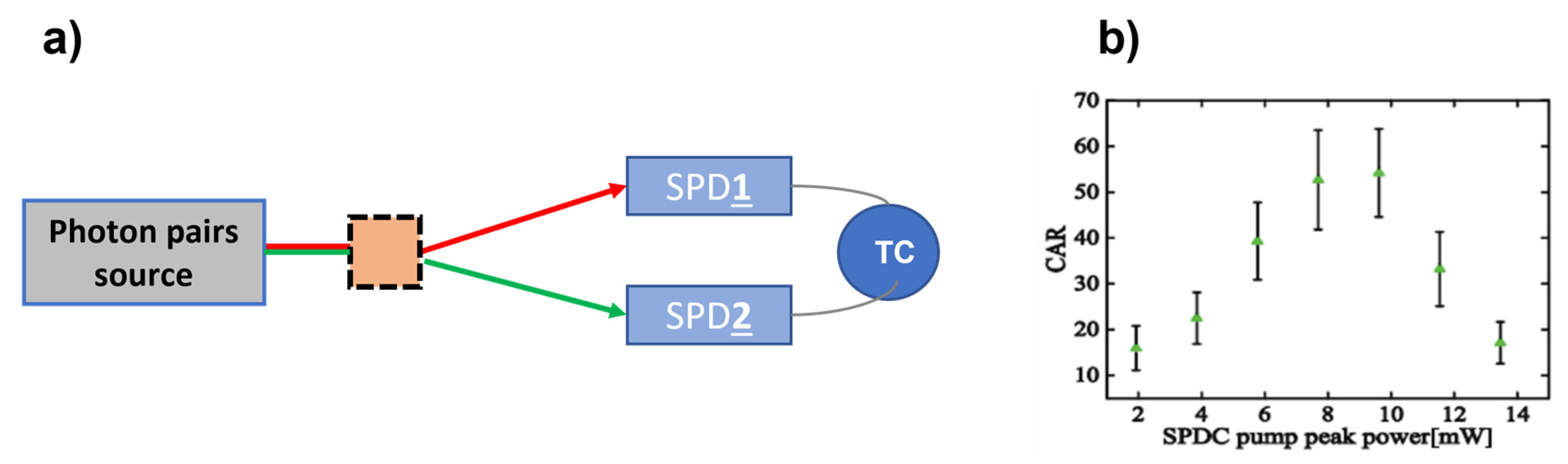
3.1. Coincidence Measurements and CAR

The coincidence measurement between the signal and the idler photons is performed to demonstrate the time-correlated nature of the generated photon pairs. It involves the measurement of both the true coincidence counts and the background or accidental counts with the typical set up shown in Figure 3a:
The signal and idler photons generated through the non-linear process are spatially separated using a specific component (graphically represented by the orange square), for example a dichroic mirror [38], a parabolic mirror for far field separation [39], or a polarizing beam splitter, according to the specific experimental set up. The signal and idler photons are then detected by two single photon detectors. Time-tagging electronics is used to record the difference in their arrival time and build a coincidence plot, showing the coincidence counts as a function of the arrival time difference of the signal/idler photon on the detectors. At zero time difference a coincidence peak is expected to demonstrate the generation of the photon pair. The true coincidence counts result from the simultaneous detection of the photon pair generated by the same pump pulse, corresponding to the coincidences in the zero-delay peak. It is linearly dependent on the pump power. The accidental coincidence is the rate of coincidence not resulting from the detection of both photons from a single pair, but from uncorrelated photons from two different SPDC processes. It depends quadratically on the pump power.
The signal-to-noise ratio in coincidence measurement is referred to as coincidence to accidental ratio (CAR). It is calculated using the coincidence plot as the number of coincidences in the peak within a certain coincidence window (N12) divided by the average of the background counts on the same time window taken away from the peak (Nacc):
C A R = N 12 N a c c ,
The characterization of the CAR for a SPDC process is carried out studying the variation of the CAR as a function of the pump peak power in order to find the best pump power maximizing it. The typical trend is reported in Figure 3b and shows a trade-off behavior with the pump power. For low pump power, the CAR is lower due to the low photon-pair generation which has to be compared with the overall noise and dark count rates of the entire detection system employed. Above a certain threshold the CAR decreases with the pump power due to the multiphoton pair emission in SPDC, which consists in the simultaneous generation of more than one pair (per pulse) that increases the probability of accidental-coincidence detection.

3.2. Purity and Second Order Correlation Function

Ideally, a single photon source would emit a single photon every time with zero probability of multiple photon emission. The probability of single photon emission is defined as source purity [37]. The characterization of the source purity is performed measuring the second order correlation function g(2)(τ), where τ is the time delay between the idler and signal photons, which quantifies the multiphoton component with respect to the single-photon component. The experimental set up commonly used to measure g(2)(τ) is a modified version of the Hanbury–Brown Twiss interferometer used for the correlation measurements, adding a third single photon detector in the idler arm, as shown in Figure 4:
The signal and idler photons exiting the photon pairs source are spatially separated, as explained in the previous section. A single photon detector is used to detect photons in the signal arm, while in the idler arm a 50/50 coupler is used and followed by two SPDs. The signal side detector SPD1 is used as the heralding reference: when one photon of the pair is recorded on SPD1, it heralds a correlated photon in the experiment, which can be registered either on SPD2 or SPD3. As a result, if only one pair is generated, a zero simultaneous event will be registered on all three SPDs.
The second-order correlation function is then described by:
g H 2 τ = N 1 N 123 τ N 12 N 13 τ ,
where N1 are the single counts registered on the reference detector on the signal arm, N12 and N13 are two-fold coincidence counts and N123 are three-fold coincidences among all three SPDs. In the ideal case, for a single photon source the second order correlation function at 0 delay arrival time is g H 2 0 = 0 , since N123 is zero. Experimentally, background photons and dark counts of the detector can cause false coincidence counts, altering the statistics, making necessary a postprocessed analysis of the raw data for correction. Moreover, the finite time response of the detectors can obscure g(0).

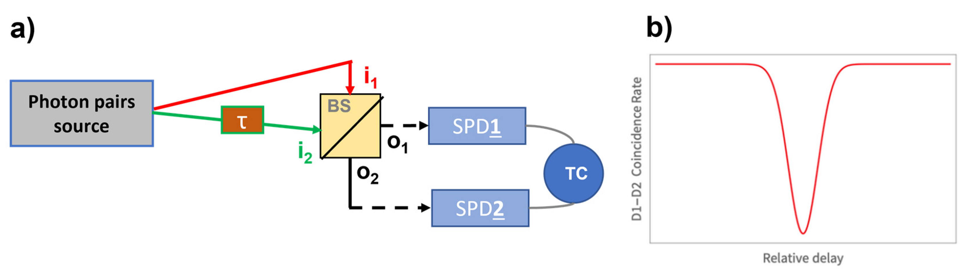
3.3. Indistinguishability with HOM Interference
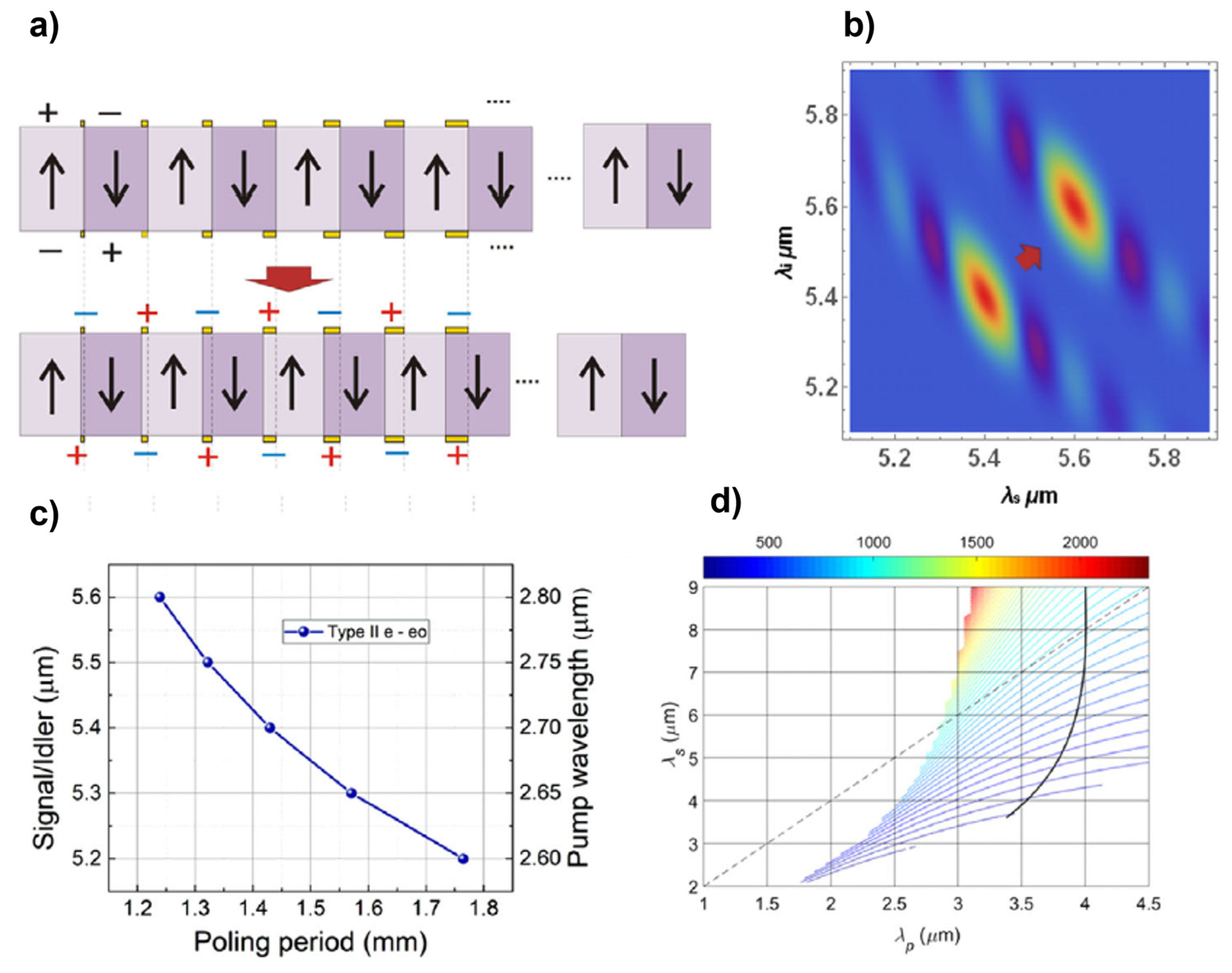
Many applications of quantum photonics require the indistinguishability of the emitted photons, which means that photons are emitted in the same quantum state, making possible the quantum interference between separately generated photons. The standard test to verify the indistinguishability of photons is to perform two-photon Hong–Ou–Mandel interference [40,41,42] with the apparatus shown in Figure 5a. The two twin photons, created for example in the SPDC process, impinge on the two different input ports of a half beamsplitter and the coincidence counts of photons coming from the output ports are detected by two SPDs. One path of the interferometer can be changed in length so as to make the photons distinguishable by different arrival times on the beam splitter.
Two photons in the same pure quantum state incidenting on the two inputs of the 50:50 beamsplitter with spatial and temporal overlapping, will show quantum interference and will leave the beamsplitter together in the same output mode. Therefore, coincidence counts in the different outputs will decrease to zero. For such an effect, a dip known as the HOM dip (Figure 5b) can be measured in the coincidence counts by sweeping the arrival time difference of the input photons to vary the distinguishability of the photons. The depth of the HOM dip reflects the degree of indistinguishability of the two input photons which is evaluated by the well-known HOM visibility. Given the rates of minimum and maximum coincidences (Cmin, Cmax) across the dip, the visibility is calculated as VHOM = (Cmax − Cmin)/Cmax.
Experimentally, some measurement non idealities, including residual multiphoton emission probability, unbalanced beamsplitter, the finite detector time response, the detector count rates, worsen the HOM visibility evaluation from the raw data.

4. SPDC in the MIR

Driven by the outstanding results obtained in the generation of photons from UV to NIR using SPDC with Beta barium borate (BBO) [43,44], Bismuth Borate (BiBO) [45,46], Periodically Poled Lithium Niobate (PPLN) [47,48,49,50] and Potassium titanyl phosphate (PPKTP) crystals [51], much theoretical and experimental effort has been spent in the last decades in the development of single or entangled photon sources in the Mid Infrared range by using an SPDC process. LN and KTP are birefringent oxide crystals widely exploited for SPDC in the visible and NIR range, where they are transparent, and can be easily pumped by commercial lasers, such as the 800 nm Ti:sapphire, the 1040 nm Yb:fiber and the 1550 nm Er:fiber lasers. Their exploitation in the MIR range is prevented by the multiphoton absorption losses above 4.5 µm [52]. Therefore, the first essential requirement to extend SPDC to the MIR, is the investigation and fabrication of novel non-linear materials satisfying some essential features to be implemented in a SPDC process: large nonlinear coefficient, MIR transparency range, as well as intrinsical group velocity-matched wavelengths in the MIR range. Numerical simulations on the potential capability of these materials to generate single photon at MIR wavelengths support and guide their experimental implementation, giving information on the experimental parameters and conditions to obtain the desired phase-matching properties. In the following paragraphs, the main results regarding numerical simulations with the most promising novel materials, as well as the experimental results on the generation of MIR photons will be presented.

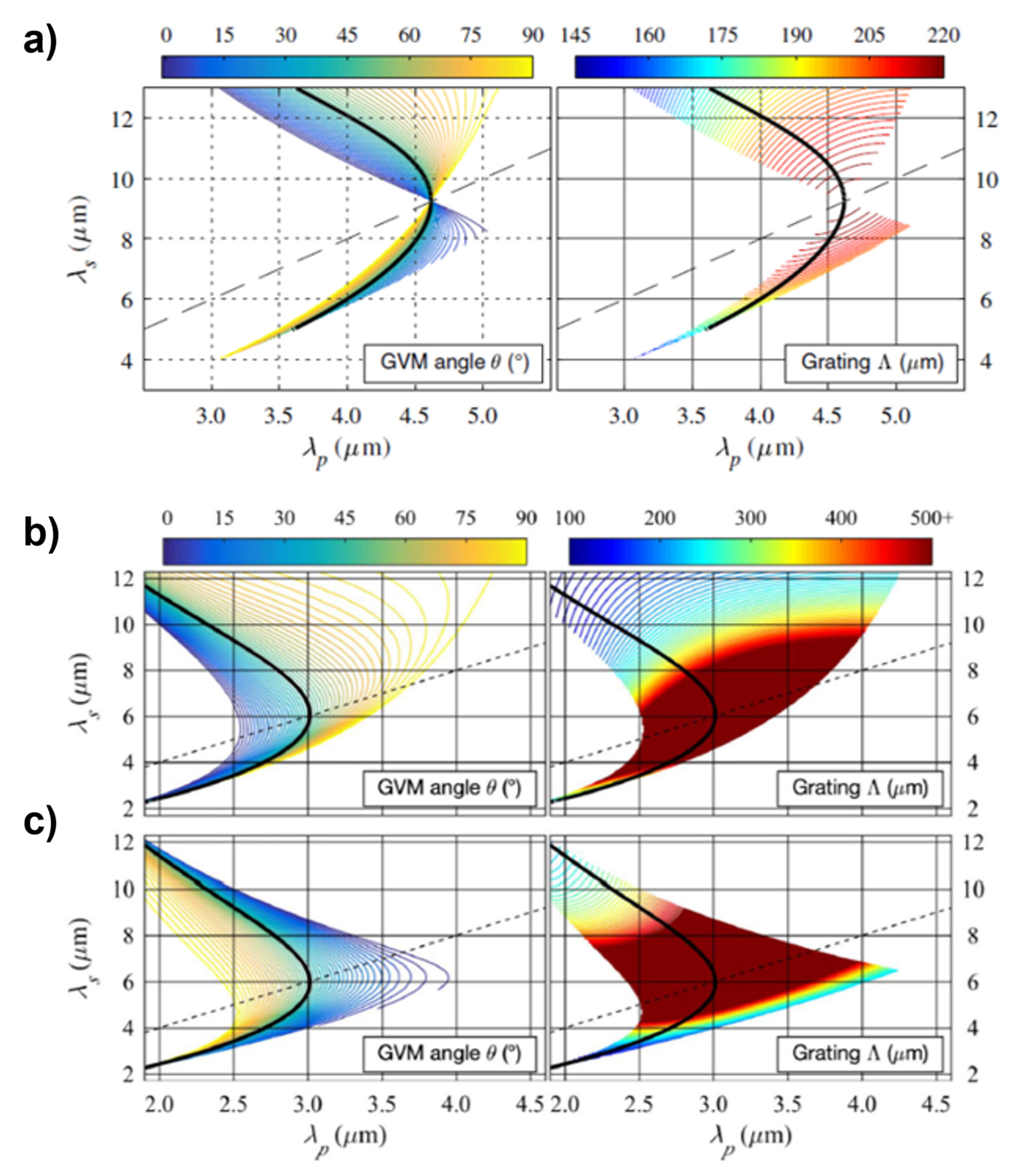
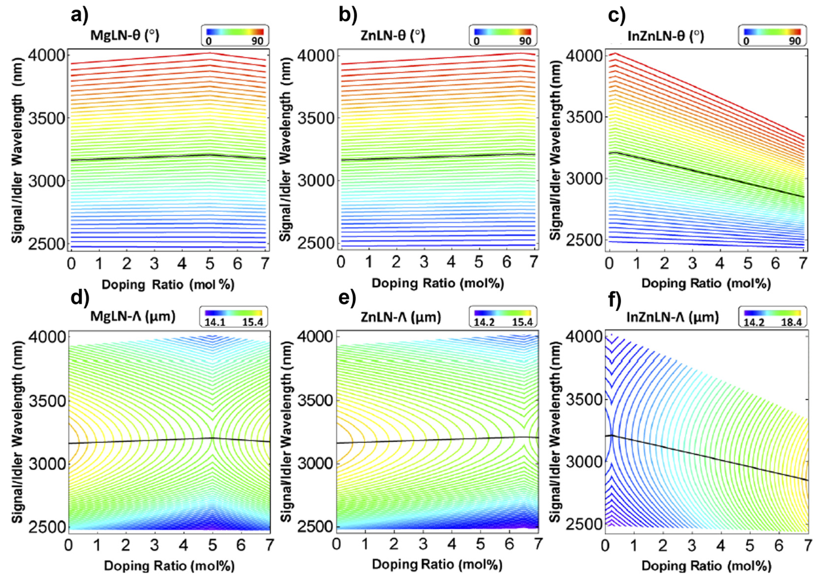
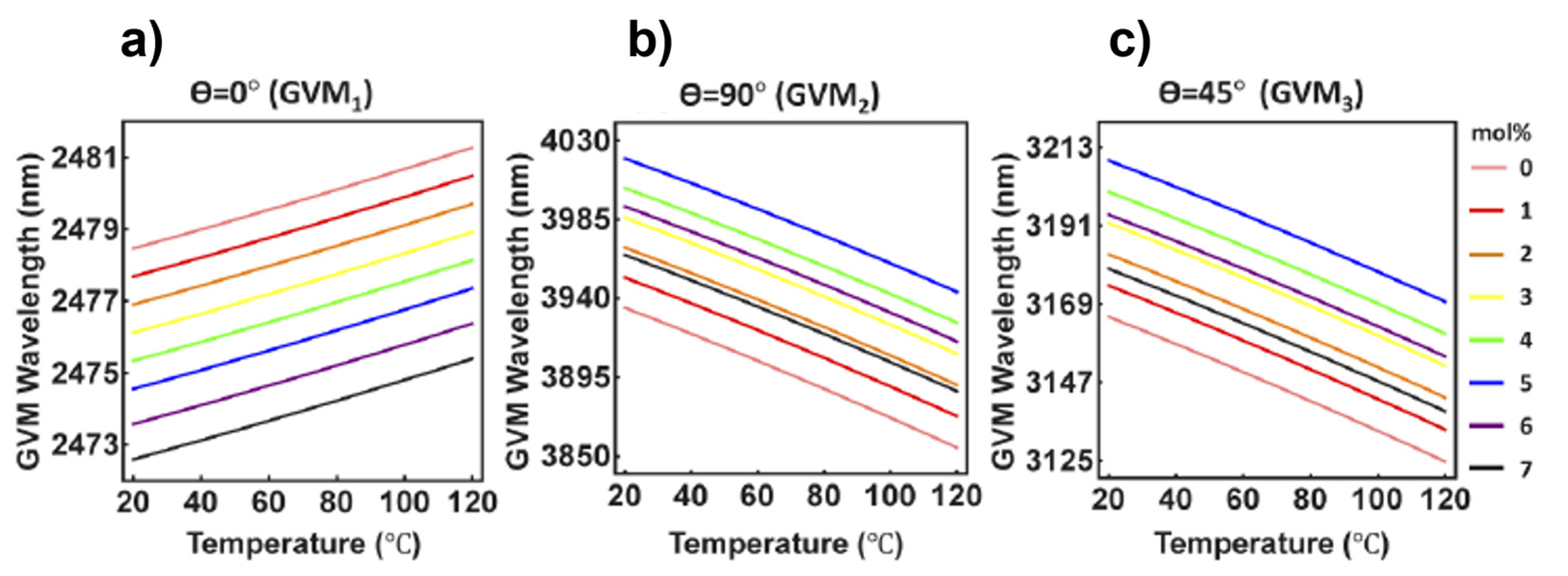
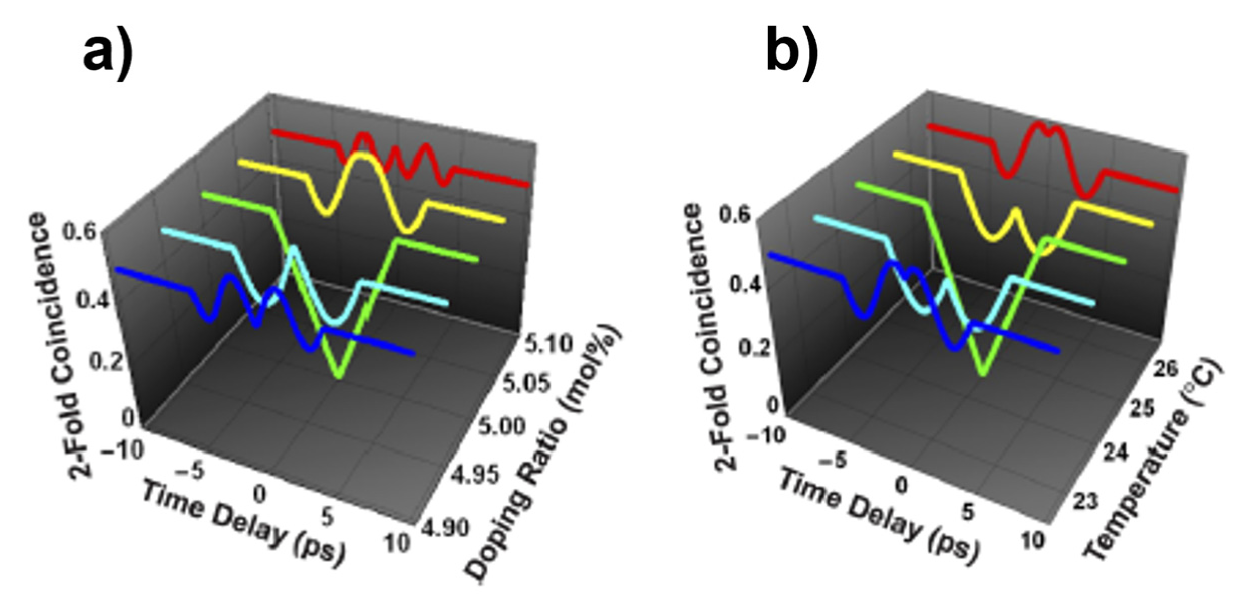
4.1. Numerical Study

Numerical studies on the parametric downconversion are a powerful tool to investigate the capability of generating biphotons at the desired wavelengths with proper non-linear materials, giving at the same time information on the most suitable experimental conditions to achieve high efficiency.
In particular, the joint spectral amplitude (JSA) of the emitted photon pairs in SPDC characterizes their structure and joint spectrum as well as their quantum correlation, assuming a key role in the analysis and control of the characteristics of the generated quantum state of light [53]. JSA can be calculated as the product:
f ω s ,   ω i = α ω s ,   ω i Φ ω s ,   ω i ,
where α is the pump envelope function (PEF) and Φ is the phase-matching function (PMF). Equation (10) shows that the structure of the generated idler/signal photons is affected by the shape and profile of the pump beam used in SPDC. Assuming a Gaussian-distribution, the PEF can be expressed as
α ω s ,   ω i = e x p 1 2 ω s + ω i ω p σ p 2 ,
where the frequencies ω s ,   ω i ,   ω p are the ones satisfying the energy conservation in Equation (1), and σ p is the bandwidth of the pump.
The PMF function can be expressed as:
Φ ω s ,   ω i = S i n c Δ k L 2 ,
where L is the length of the crystal and
Δ k = k p k i k s ± 2 π Λ = 2 π n λ p λ p n λ s λ s n λ i λ i 1 Λ ,
is the wave vector mismatch, n(λ) is the refractive index for the signal, idler and pump photons, described by the Sellmeier relations for every crystal [54,55].
The crucial parameter involved in the simulations is the angle θ between the ridge direction of PMF and the horizontal axis in the signal–idler frequency space, which is determined by:
                                        D = tan θ = V g , p 1 ω p V g , s 1 ω s V g , p 1 ω p V g , i 1 ω i ,
where V g , x is the group velocities of the photons, and the parameter D is called dispersion parameter. The experimental approach is to tune the experimental parameters in order to fulfill the group-velocity matching conditions, which determines the JSA’s shape. In particular, using Equation (14), three group-velocity matching conditions can be identified: the fully asymmetric GVM1 and GVM2 corresponding to the cases θ = 0 ° and θ = 90 ° , and the symmetric GVM3 corresponding to θ = 45 ° . The conditions GVM1 and GVM2 provide a spectrally uncorrelated biphoton state with high heralded-photon purities, but the signal-idler photons are distinguishable due to their different bandwidths. In particular, the GVM3 has a symmetric distribution along the antidiagonal direction, which is fundamental for high visibility HOM interferences. The photons produced under GVM3 are indistinguishable, but the uniform nonlinearity profile of the crystal causes residual correlations which affect the photons spectral purity [56].
Different studies are focused on the study of the group velocity matching region in different materials. In [52] two categories of novel non-linear materials were investigated, consisting of birefringent chalcopyrite crystals, including zinc germanium phosphide (ZGP) and cadmium silicon phosphide (CSP), and quasi-phase-matched semiconductors, as orientation-patterned gallium arsenide (OP-GaAs). These materials exhibit strong two-photon absorption at lower wavelength, but excellent transparency in the MIR, together with significantly larger non-linear coefficients compared to the conventional LN and KTP. With respect to oxide crystals, semiconductors offer excellent conductivity and high non-linear coefficient, and can be grown with high purity.
The phase-matching condition in Equation (13) was numerically solved using a range of pump wavelengths above the two-photon absorption limit and for various non-linear materials. For each wavelength and material, the grating period required to achieve Δ k = 0 and the dispersion parameter D = tanθ were calculated, considering Type-0, Type-1 and Type-2 downconversion. An illustrative example of the obtained results is reported in Figure 6, which shows the signal wavelength versus pump wavelength with corresponding GVM angle θ (left) and grating period Λ (right) for type-0 SPDC in OP-GaAs (Figure 6a) and type-2 SPDC in ZPG (Figure 6b,c). Solid red areas represent grating period longer than 500 µm, where birefringent QPM is possible; the dashed line indicates degeneracy, while the black line corresponds to θ = 45°, which results in highly indistinguishable photon pairs; the plotted boundaries indicate areas of high spectral purity (θ = 0°, 90°). The numerical results in Figure 6 show the capability to generate MIR single photons at wavelengths up to 13 μm in nondegenerate PDC type-0 quasi-phase-matching in OP-GaAs and up to 7.4 μm in a degenerate configuration type-2 birefringent phase-matching in ZGP.
A parallel strategy to the implementation of novel materials is the proper modification and engineering of the traditional materials used in NIR SPDC. The effect of doping on the generation of spectrally uncorrelated biphotons in the MIR range from SPDC was theoretically investigated in [57] using doped PPNL crystals: MgLN, InZnLN and ZnLN. This work showed how the kind of dopants and the doping ratio can influence the Sellmeier equations, resulting in a substantial impact on the GVM wavelengths, offering a degree of freedom to manipulate the biphoton state at MIR range. In this study the angle θ and the corresponding poling period Λ were calculated under type-II, type-I and type-0 phase matching conditions for different doping ratios. Figure 7 shows the results obtained for the type-II phase-matched SPDC in the degenerate case: the θ angle is shown as a function of the doping ratio in the range 0–7% and of the signal/idler wavelengths for MgLN (Figure 7a), ZnLN (Figure 7b) and InZnLN (Figure 7c) crystals. Figure 7d–f shows the corresponding poling periods for each crystal.
Figure 7 shows how fixing the angle θ is possible to obtain different signal/idler wavelengths, changing the doping ratio of the crystal. In particular, for InZnLN (Figure 7c) a tunable wavelength range of 678.7 nm can be achieved for the GVM2 wavelength ranging from 4006 nm to 3342.9 nm varying the doping ratio from 0 to 7%, respectively. The possibility to achieve a tuning of the wavelengths much higher than the 100 nm reached with conventional temperature tuning represents an essential feature for quantum state engineering in the MIR range. By improving the doping ratio above 7 mol% the wavelength tunability could be further improved.
The temperature represents another experimental parameter to be controlled, since it influences the phase-matching conditions in the crystals. This influence can be investigated by calculating the GVM wavelengths as a function of the temperature, using the temperature dependent Sellmeier equations, as performed in [57]. Figure 8 [57] shows the GVM1 (a) GVM2 (b) and GVM3 (c) wavelengths for MgLN crystals when changing the temperature in the range (20°, 120) °C for different doping ratios: it can be concluded that the temperature increase mainly affects the GVM2, with a corresponding linear decrease of 78 nm, while GVM1 is the less sensitive, with a linear increase in wavelength of only 2.8 nm.
The influence of the doping ratio and the temperature on the biphotons generated through SPDC affects interesting practical applications, such as the HOM interference between the signal and idler from the same SPDC source. The simulated process in Figure 9 [57] shows how starting from the HOM interference pattern from a signal and idler from the same Mg (5 mol%) LN crystal at 24.5 °C with a 100% visibility (green curve), the variation of the doping ratio (Figure 9a) or the temperature (Figure 9b) causes an oscillation of the interference patterns.
The possibility of reconfigurable operation of single photon sources is attractive for many quantum applications, such as information processing as well as free-space quantum communication, giving the capability of dynamically modifying the SPDC single photon wavelengths with a single crystal. In [58] a numerical study of reconfigurable MIR single photon sources based on functional ferroelectric lead magnesium niobate-lead titanate (PMN-0.38PT) crystal were formed, revealing the existence of phase-matching conditions giving spectrally pure single photon at 5–6 μm. The straightforward advantage of using this material is the possibility to dynamically repoll it at ambient conditions with fields as low as 0.4 kV mm−1, differing from the most used ferro-electric crystals such as LiNbO3 or KTiOPO4 which lack tunability of the poling period after their fabrication. Changing the poling period means having the possibility of changing the wavelengths of the single photons, to turn on and off the SPDC generation as well as to remodel the wave-packets of the photons. A detailed investigation of all possible collinear configurations of photon wavelengths and polarization was performed in [58], setting as input parameters the pump center wavelength (2.7 and 2.88 μm) and the length of the crystal (25 mm) in order to match the spectral width of the PEF. The most valuable results were obtained investigating the type II PDC, showing the possibility to obtain degenerate GVM for PMN-PT with PMF inclination 0° for a high purity biphoton state. Compared to the type-I and type-0 SPDC, a longer poling period of 1.429 mm was obtained, which is an advantage since it facilitates technologically the implementation of the ferroelectric switching functionality of the poling order. This feature can be attained with the implementation of an electrode-patterned mask along the crystal length: the mask provides a tool to modify the poling period of each particular domain selectively and on-flight. Figure 10 [58] shows an illustrative example of the switching mechanism of the poling period for a potential MIR free-space QKD application where the wavelength of the created single photons needs to be changed from 5.4 to 5.6 μm, which corresponds to a switching of the poling period from 1.429 mm to 1.239 mm. Two photon pump wavelengths of 2.7 and 2.8 from a tunable OPO are considered as a pump source.
Given the initial crystal length with poling period 1.429 mm corresponding to 5.4 μm generated photons, a prefabricated electrode mask is applied as in Figure 10a. The application of a proper voltage to each electrode pair deposited on the edge of the corresponding domain causes the stretching or contraction of the domain in order to obtain the desired poling period. To ensure a uniform variation of the poling period across the entire crystal, the mask is fabricated with a linear gradient elongation, starting from the first electrode length and moving along the crystal. The strength of this method relies on different practical advantages. The proposed design is fully reversible, with the possibility to return to the previous poling period by switching the polarity of the electrode mask. The rate of dynamic domain repolling can reach the ns scale. Moreover, by designing a proper electrode mask, a wide range of signal/idler photon wavelengths can be achieved as illustrated in Figure 10d.

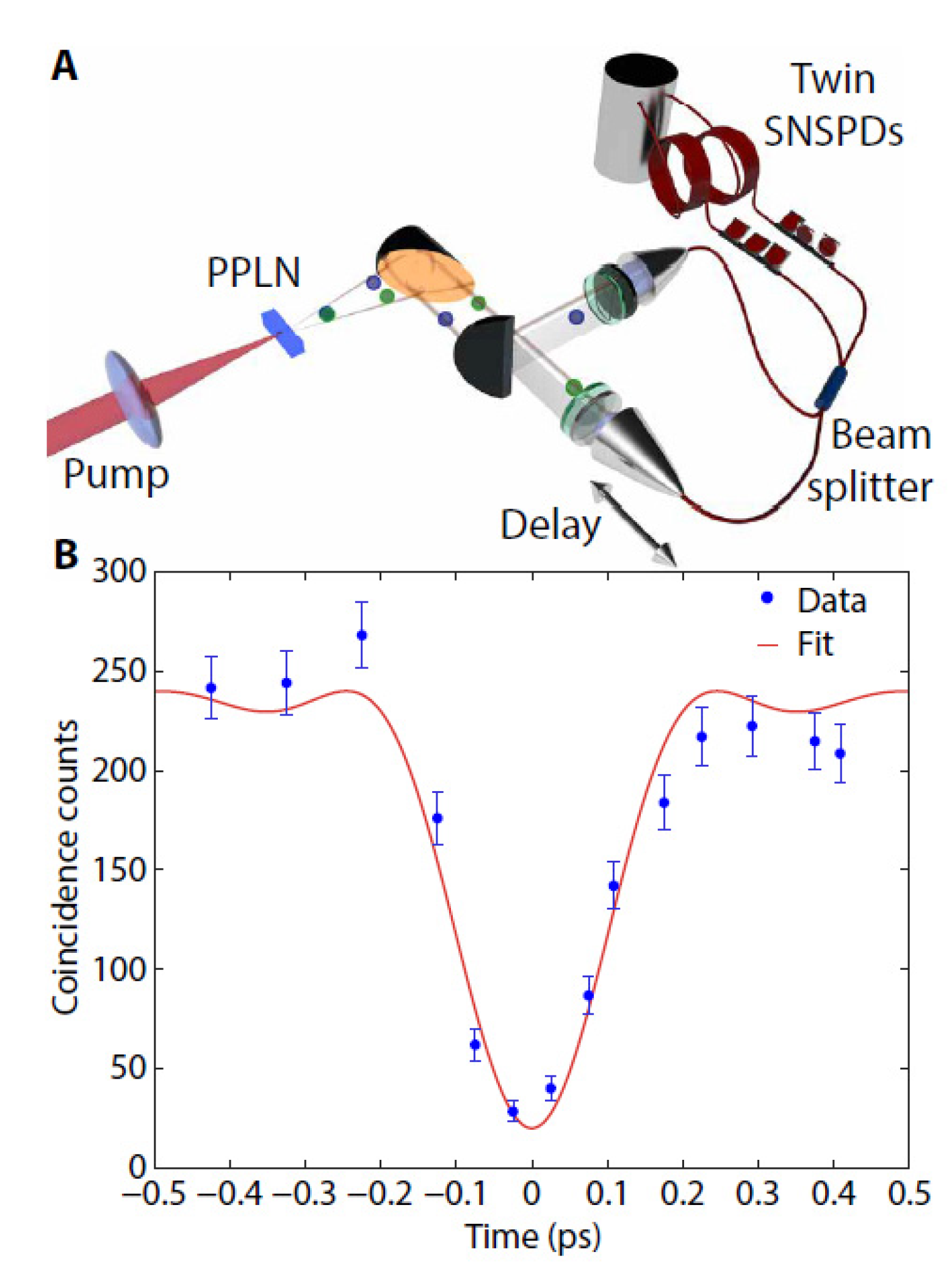
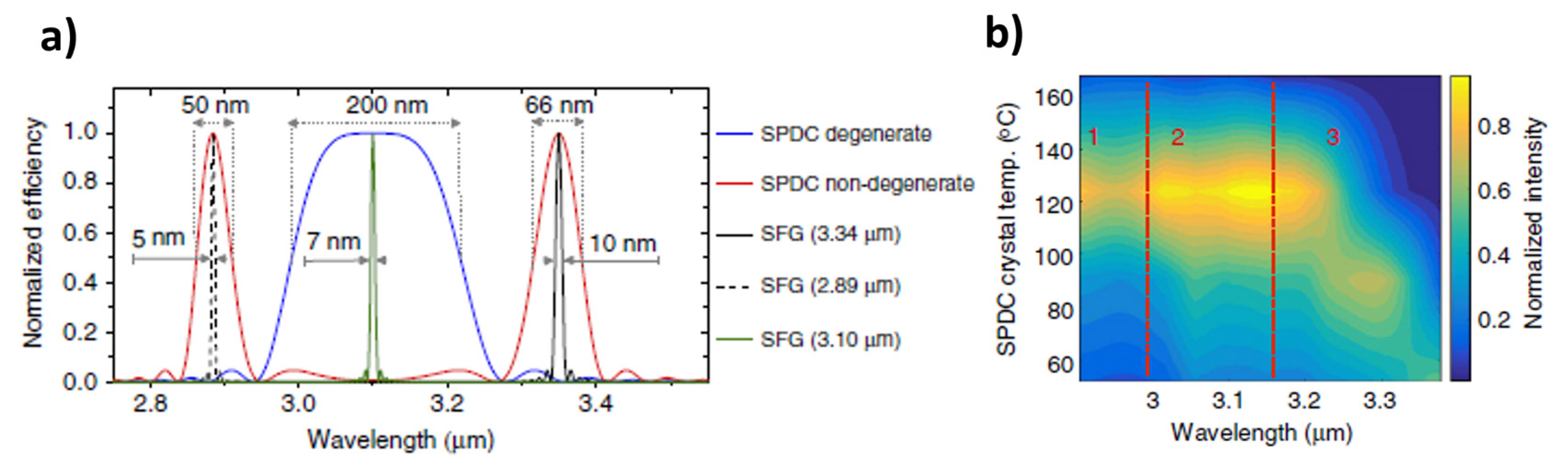
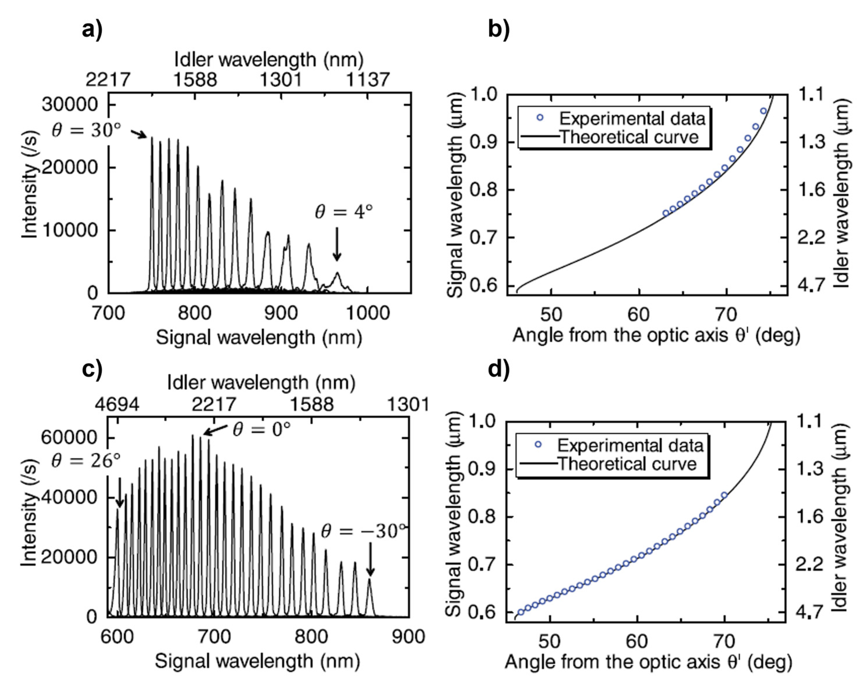
4.2. Experimental Results

Together with the large effort in fabricating novel materials and simulations, the first experimental results were achieved in the last years.
In [39] the first SPDC generation and characterization of indistinguishable degenerate photon pairs at 2090 nm was proved, together with the demonstration of two photon quantum interference and polarization entanglement. The pump laser was a compact Yb-based fs fiber laser at 1045 nm, emitting a train of pulses with an average power of up to 2.5 W at 80 MHz repetition rate. A complete characterization of the source was performed. The generation efficiency of SPDC was quantified for a type 0 phase-matched configuration using a 1 mm-long periodically poled, magnesium-doped lithium niobate crystal (MgO-PPLN). The following properties of the crystal were examined: the selection of the crystal length has to ensure both maximum conversion efficiency, with minimal temporal separation between the pump and the generated SPDC fields; the ferroelectric poling of 30.8 μm was determined to guarantee coherence between the phase of the pump field and of the generated photon-pair for the entire length of the crystal and over a broad bandwidth; the temperature was stabilized at (30 ± 0.1) °C.
As described in Section 3, the first step to characterize the photon source is the demonstration of the generation of correlated photon pairs using the experimental setup similar to the one in Figure 3 to reconstruct a coincidence plot. In this experiment, superconductive nanowire single photon detectors (SNSPDs) were implemented to detect single photons and time-tagging devices to record their arrival time. The obtained histogram showed maximal coincidences at zero delay time. A maximum CAR of 180 ± 50 at 5 mW of input pump power was measured for 30 min integration time, then it decreases with the pump power, PP, as 1/Pp due to the increasing probability of generating multiple photon pair per pulse resulting in increased accidental counts.
The quality of indistinguishability of the generated photons investigated by studying the two-photon interference using the Hong–Ou–Mandel interferometer scheme described in Section 3.3. Figure 11A [39] shows the experimental setup for characterizing the two-photon interference, obtaining the characteristic HOM dip in correspondence of zero delay between the two input ports of the beam splitter, as shown in Figure 11B. The high visibility of 88.1% achieved in the experiment allowed the demonstration of the photon indistinguishability.
An interesting application of this source is the generation of polarization-entangled photons, which are an essential part of QKD schemes. To this end, the Mg-PPLN crystal was fabricated 200 μm long with a poling period of 13.4 μm in order to achieve PM at 110 °C for type-II SPDC. The violation of CHSH-Bell inequality with a Bell parameter S = 2.20 ± 0.09 represents the proof of the entanglement between idler and signal photons, paving the way for technological implementations of QKD in the 2 μm range. Further improvements of the estimated entangled photon generation rate of 200 kHz are strictly connected to the improvement of the detection efficiency at 2.1 μm as well as to the reduction of in-line losses.
In [59] a PPNL crystal was used to generate twin photons at 3.1 μm in a free-space set-up at room temperature. A continuous-wave infrared laser at 1.5 μm, amplified by an erbium-doped fiber amplifier, pumped a 10 mm long PPLN crystal having a poling period of 34.48 μm. As already pointed out, both the crystal poling period and temperature are important experimental parameters to be optimized and controlled to satisfy the PM condition at the desired wavelength. Since the phase-matching condition is temperature dependent, a fine-tuning of the phase-match condition was performed by changing the temperature of the PPLN crystals, which were mounted in ovens, by temperature controllers. For a given poling period, different SPDC processes can be achieved, as shown in the simulated downconversion spectra in Figure 12a [59] obtained at the fixed temperature of 135 °C (blue curve), corresponding to degenerate SPDC at 3.1 μm, and 68 °C (red curve), corresponding to non-degenerate SPDC. For the conservation of the energy, two side lobes symmetrically distributed around λdeg = 3.1 μm are visible in the spectrum for the non-degenerate SPDC with spectral bandwidth of 50 nm (for the 2.89 peak) and 66 nm (for the 3.34 peak); the spectral bandwidth for degenerate SPDC shows an increase up to 200 nm.
The generated SPDC photons in the MIR were detected using two upconverter modules and two Silicon Single Photon Avalanche Diodes (Si-SPADs). The experimental spectrum for the degenerate and non-degenerate processes as a function of the SPDC crystal temperature in Figure 12b [59] was measured using different poling period of the Sum Frequency Generation (SFG) crystal to scan the wavelength, labelled as 1, 2, 3. Coincidence measurements on the MIR photon pairs were performed to demonstrate the time-correlated nature of the generated photon pairs and the detection capability of the system to perform these kind of measurements. A clear peak of coincidences in time between the signal and the idler demonstrated the time correlation of the generated photons. A CAR of 15.7 ± 0.4 was measured within a coincidence window of 1.3 ns at an integration time of 10 s. At the optimal incident pump power of 70 mW the conversion efficiency of the SPDC process was estimated to be −110 dB.
Advances were obtained in [38] with the generation of high purity photon pairs through SPDC in a magnesium-doped periodically-poled lithium niobate (MgO:PPLN) waveguide with properly designed geometry and periodic poling. The main advantage of this experiment was the 3.2 µm wavelength spacing between the idler and signal photons at 780 nm and 3950 nm, representing at the same time the main challenge. Actually, the high non-degeneracy between the photons makes it difficult for the spatial-mode and phase matching in the waveguide, and requires a proper study of both the waveguide geometry to support overlapping fundamental transverse modes for all light-waves and of the periodical poling of the waveguide optical domains to offer the large phase mismatch. The fine-tuning and stabilization of the temperature gave a high −87 dB SPDC efficiency. The detection of the generated photons was realized using a fiber-coupled Silicon Avalanche Photodiode (Si-APD) for the signal photon (quantum efficiency of 12.5%, dark count rate < 1.4 Hz) and a second Si-APD detector for the idler photons (quantum efficiency 22.5%, dark count < 1.8 Hz), which are first upconverted using another PPNL waveguide pumped by 779.8 nm pulses. The measured maximum CAR was 54 ± 7 at a peak power of 9.7 mW. This value is limited by the uncorrelated noise photon as well as the dark counts of the upconversion detection system. The maximum CAR corresponds to true coincidence counts of 275 within an integration time of 300 s, which results in a photon pair production rate of about 9.4 × 10⁴ pairs per second with spectral brightness of 4.4 × 10² pair/(s nm mW). The generation of MIR idler photons at 3950 nm can be heralded, by detecting the 780 nm photons, with a g2(0) = 0.08 ± 0.015 representing a high-quality single photon source in the MIR. This source is particularly appealing for quantum secure direct communication protocol with quantum memory, adopting the idler MIR photon for a free-space quantum channel and storing the signal photon at 780 nm with a rubidium-based quantum memory. Other possible applications are free-space QKD based on time–energy entanglement, as well as for single photon microscopy and quantum-enhanced spectroscopy for sensitive biomedical imaging and diagnostics.
An attractive feature for a wide range of applications is the capability to realize a photon-pair source with wavelength changeable in the MIR range. In [60] an experimental demonstration of wavelength variable generation and detection of photon pairs in the VIS and MIR region (2–5 μm) via SPDC was reported. The attractive innovation is the possibility to continuously change the wavelength of the signal and idler photons in the range (600, 965) nm and (1186, 4654) nm by changing the angle of the non-linear crystal as in Figure 13 [60], which correspond to tune the PM condition. LiNbO3 doped with 5-mol% Mg(O) was used as a non-linear crystal since it is transparent in the 0.42–5.2 μm range and shows a high non-linear optical efficiency. Two LiNbO3 crystals were used with different cut angles ϕ, defined as the angle between the optic axis (OA) and the crystal surface normal.
Figure 14 [60] shows the signal spectra acquired using a spectrometer and a CCD camera, while rotating the angle θ for two crystals as shown in Figure 13b, where θ represents the angle between the pump direction and the crystal surface. The idler wavelengths corresponding to the signal ones are reported in the top axes.
Figure 14a,c show the spectra of SPDC photons generated from crystal 1 and crystal 2, respectively: for the same initial position of the crystal with respect to the pump (θ = 0°), different initial wavelengths were generated; rotating the crystal both in positive and negative directions, the wavelength of the generated photon changes. Figure 14b,d show the dependence of the center SPDC wavelength generated by crystal 1 and 2 on the internal angle θ’ from the OA, showing the capability to generate idler photons in the range (1186, 1824) nm and (1436, 4694), respectively. Further investigation using two SNSPDs for the VIS and IR photons with different detection efficiencies showed that the photon pair generation rate is ~105 s−1 per mW of pump power in a wide wavelength range up to 2000 nm.

5. FWM in MIR

FWM in silicon quantum photonics emerged as an optimal technology offering the features of integration, miniaturization and manufacturability required by many applications in quantum sensing and metrology [61]. Silicon-on-insulator (SOI) waveguides platforms are particularly attractive since they are compatible with complementary metal-oxide semiconductor (CMOS) technology, taking the advantages of advanced on-chip integration of various electrically and optically controlled components [62] and of mature fabrication methods which facilitate reliable and reproducible results [63]. Wavelength-division multiplexing schemes have been demonstrated on a silicon micro-ring resonator, enabling parallel distribution of photon pairs at telecommunication multiwavelength channels, with potential benefits for the extension of the information capacity of a quantum network for parallel QKD [64]. Moreover, in the general framework of moving from NIR towards MIR integrated optics, SOI photonics offer three main advantages if operated at wavelengths greater than 2 μm, with respect to the implementation at the 1550 nm wavelength. First, the main source of losses limiting the heralding efficiency of SFWM single photon sources at 1550 nm is the intrinsic two-photon absorption (TPA) [65,66,67]. It consists of the excitation of a crystal electron by two photons. The energy of two photons at 2.1 μm is not sufficient to excite a crystal electron [68,69]. Secondly, the photon-pair generation at 2.1 μm is more efficient, thanks to the presence of a peak in the non-linear refractive index. Finally, a reduction of the linear loss due to Rayleigh scattering off etched waveguide sidewalls occur at long wavelength [70,71]. These strength points moved the research to develop and optimize silicon waveguides able to generate entangled photon pairs at 2.1 μm, designing the waveguide in order to guarantee efficient SFWM in accordance with the equations in Section 2.2.
There are two types of FWM that can be realized [72]: the most conventional is intra-modal FWM, where the conversion of two input pump photons into an idler and a signal involves only one waveguide mode. Differently, in inter-modal SFWM the phase matching is achieved exploiting the different optical spatial modes of a photonic waveguides with different chromatic dispersion.
In [73] MIR, intra-modal FWM was realized in a silicon waveguide. The design was optimized based on the simulations of the dependence of the waveguide group-velocity dispersion (GVD) parameter β2 and of the effective modal area Aeff with the waveguide width at λ = 2.071 μm, as shown in Figure 15 [73].
Since for efficient intra-modal FWM the GVD must be anomalous or zero (β2 ≤ 0), the optimal waveguide width of 510 nm was selected. With this geometry the phase-matching of the source was demonstrated measuring stimulated FWM on an optical spectrum analyzer. Figure 15c [73] shows the power spectral density of the pump and stimulated emission for different seed laser wavelengths, confirming that phase-matched FWM was observed over 60 nm. Spontaneous FWM in the waveguide was used to obtain a bright source of quantum-correlated photon pairs, whose characterization showed a generation probability of 0.28/W2 and a maximum CAR of 25.7 ± 1.1. On-chip quantum interference was demonstrated using a time-reversed HOM experiment, with the experimental setup and waveguide circuit shown in Figure 16a,b [73].
The picosecond-pulsed laser centered at 2.0715 µm was injected into the fundamental TE mode of the waveguide with a vertical grating coupler. The pump field was equally split between the two photon-pair sources, which are coherently pumped and the relative phase ϕ between the two arms was changed using a thermo-optic phase modulator. The biphoton state then interfered on a balanced directional coupler. Coherent pumping of both sources produced SFWM photon pairs in superposition. Figure 16b reports the experimental results, showing characteristic half period interference fringes in the coincidences with the variation of the on-chip phase. This quantum interference showed a net visibility of V = 0.993 ± 0.017.
In [74] the demonstration of a SOI waveguide chip source of heralded MIR single photons based on inter-modal SFWM was reported. The first straightforward advantage of this operation mode is that the signal and the idler photons are generated on different waveguide modes, making it possible to separate them easily with high efficiency using an on-chip mode converter. The heralding efficiency was enhanced with respect to traditional intra-modal SFWM thanks to the generation of photons in discrete bands, which prevented the use of narrowband filters to select the wavelength of signal and idler. The pump was a standard 1550 nm pulsed laser which was easy to integrate in a chip and the MIR detection was performed by means of an upconversion system, avoiding the use of MIR technology. Moreover, intermodal FWM has the advantage of not requiring anomalous group velocity dispersion (GVD) [75], commonly researched for intramodal FWM to achieve phase matching [76,77]. This results in easier handling of the phase-matching condition [78], higher flexibility and larger spectral conversion.
The apparatus to realize intramodal FWM in a waveguide is shown in Figure 17 [74].
The pump, split in the TE0 and TE1 modes, reached the multimode waveguide where the inter-modal SFWM generated the signal photons in the TE1 modes at 1259.7 ± 0.5 nm and the idler photons in the TE0 at 2015.2 ± 1.5 nm for the conservation of the energy. This large detuning offers additional advantages for the pump and Raman noise rejection with broadband filters. A model of the process was proposed to evaluate the detection probabilities per pulse for idler, signal, coincidences and accidentals which are quadratic with the pump power for SFWM. In the model all the non-linear processes taking place in the waveguides were considered, including the main losses influencing the actual generation and transmission efficiency of the pairs: the already discussed TPA, the cross two photon absorption (XTPA) and the free carrier absorption (FCA). TPA affects almost only pump photons, while XTPA occurs between one pump photon and one signal/idler photon. As a result, the probabilities of detection are not quadratic with the input pump power, as predicted by the theory. The non-linear response of the idler detector must be modelled as well. A generation probability of (0.7 ± 0.1) W−2 and intrinsic heralding efficiency of 59 ± 5% were measured. The characterization of the CAR lead to a maximum value of 40.4, while the sub-Poissonian statistics of the source was demonstrated with a measured g(2)(0) = 0.23. The measured performances demonstrates the promising perspectives of the new approach of inter-modal SFWM for bright and efficient sources of correlated photons in the MIR, realizing a low cost, efficient and integrated solution for quantum MIR photonics, without the need for MIR technologies.

6. Conclusions

The generation of single photons and correlated photon pairs is essential for many quantum applications. In this review the results of the state of art regarding MIR sources were presented focusing on the two most promising non-linear processes of spontaneous parametric downconversion and four wave mixing.
Recent advances in the fabrication of non-linear materials stimulated the development of numerical simulations aimed at investigating how to exploit them to produce and manipulate MIR single photons generated through SPDC. Novel materials as ZGP, CSP, OP-GaAs, PMN-PT show a large nonlinear coefficient, MIR transparency range, as well as intrinsic group velocity-matched wavelengths in the MIR range. MIR single photons can be generated at wavelengths up to 13 µm through non degenerate type-0 SPDC in Op-GaAs and up to 7.4 µm in degenerate type-II SPDC in ZGP. PMN-PT is particularly attractive since it offers the possibility of dynamic control and manipulation of the MIR generated photons wavelengths changing the poling period with low coercive fields. Moreover, with respect to the bulk crystals, dielectric/PMT-PT/dielectric waveguides can be easily fabricated, moving towards an integrated quantum platform. Besides the investigation of novel materials, the proper engineering of conventional materials, such as doping the conventional PPNL with different dopants and different doping ratios, produces an instrument able to manipulate the single photon state in the MIR range. A further step would be investigating the spectrally pure single-photon generation from doped PPLN waveguides or films, which exhibit the advantages of higher non-linear efficiency, and is easier for integration and miniaturization. These simulations paved the way for quantum MIR applications such as biomedical imaging, communication, and remote sensing. Nevertheless, when moving from theoretical study to experimental implementation, technological limitations must be considered. Actually, most of the materials discussed do not show high optical quality like the conventional PPNL and PPKTP. ZGP and CSP don’t allow refractive index modification and OP-GaAs waveguides suffer from high propagation losses, making the waveguide integration difficult using these materials. Experimental implementations of PMN-PT have not been realized yet; it would require a careful and precise verification of the exact dispersion parameters for a particular PMN-PT crystal, which depends on the growth method and the doping levels.
Experimental implementations of the SPDC process for the generation of correlated photon pairs at MIR wavelengths have been based so far mainly on PPNL and MgO-PPLN. Non degenerate twin photons at 2.89 µm and 3.34 µm were generated in PPLN. MgO-PPLN was exploited in different quantum experiments: the two-photon interference and polarization-entangled photon pair generation at 2.1 µm; the direct generation and detection of a high-purity photon pair at 780 nm and 3950 nm in a MgO-PPLM waveguide; the wavelength variable generation and detection of photon pairs in the VIS and [2, 5] µm MIR region, obtained by changing the orientation of the crystal with respect to the pump direction. High coincidence-to-accidental ratios were measured for all the sources, as summarized in Table 1, indicating a strong correlation between the photons in the pairs. It is important to underline that the CAR is a measurement of the coincidence and background counts on single photon detectors. As a consequence, it strongly depends on the count rate and dark count rate of the detectors, as well as on the efficiency of the overall system, including all the optical components such as filters, beam splitters, fiber propagation, coupling with the detectors and detection losses. As a result, improvements in all these components of the system will result in further improvement of the CAR. Measurements of the second order correlation function g(2) demonstrated the indistinguishability of the reported systems. Most of the reported results are still based on bulk crystals, with the exception of [38], where SPDC and the upconversion detection system are based on a lithium–niobate waveguide, enabling the possibility to develop an integrated platform capable of hosting all necessary quantum functionality.
In parallel with the implementation of the reported SPDC experiments mainly based on bulk crystals, much work is currently focused on bringing integrated optics to MIR. In this contest, SOI photonics is a cutting-edge technology covering wavelengths up to 4 µm. Manufacturable and high-performance platforms for MIR applied quantum optics can be realized through FWM in SOI waveguides, with the demonstration of bright sources of photon pairs and high-visibility quantum interference at ~2 µm at room temperature with the intra-modal SFWM. Further improvements are required to enhance both the CAR and the interference visibility, which are currently limited by the dark count rates and the low system efficiency. New approaches based on inter-modal SFWM in SOI showed the capability to realize bright and efficient sources of correlated photons beyond 2 µm. Nevertheless, more effort still needs to be concentrated on the development of integrated photon sources to fully exploit the advantages of brightness, compactness, robustness, and low required voltages, which lead to easier adoptability in applications. Proper source engineering is required to reduce losses coming from the coupling between different elements, as well as from integrated filters, which are lossy and with low extinction, requiring cascading filters to achieve the required pump and noise suppression.
Besides the SOI waveguides discussed in this review, other platforms have been and still are investigated in integrated photonics, based on femtosecond laser micromachining in transparent material [79], or on wide-bandgap nonlinear materials, including silicon carbide (SiC), silicon nitride (Si3N4), aluminum nitride (AlN) and lithium niobate on insulator [80]. These wide-bandgap materials show low two-photon absorption and subsequent free carrier absorption, facilitating the FWM process. Silicon carbide in the 4H-SiC polytypes is attracting great interest in integrated non-linear photonics thanks to its excellent crystal quality, low material absorption, high third-order nonlinearity and high refractive index which enable strong mode confinement. To date, the most promising results have been demonstrated in the telecommunication band, with the development of a SiC photonic device for FWM with different polarization and spatial modes [81] and of soliton microcombs in an integrated SiC microresonator [82]. AlN possesses both strong Χ(2) and Χ(3) non linearities, enabling cascaded nonlinear effects including sum frequency generation, third harmonic generation and four wave mixing; its wide band gap (6.0–6.1 eV) enables applications from the ultraviolet to the mid-infrared range. High-Q and low loss AlN micro-ring resonators have been implemented to generate a frequency comb through cascaded FWM [83]. Although the results obtained in recent years with these platforms are mainly related to the near-infrared range, they offer a promising starting point for future research on their exploitation for mid-infrared photon pair generation through FWM.

Author Contributions

A.E., S.D.R. and M.S.d.C. wrote the original draft; D.D., F.S., L.S.A., D.K.P., S.D.R., A.E. and M.S.d.C. reviewed and edited the original draft. All authors have read and agreed to the published version of the manuscript.

Funding

This research was partially supported by the QOMBS project (EC H2020 Quantum FLAGSHIP GA n.820419), the QUANCOM project (MUR PON Ricerca e Innovazione 2014–2020 ARS01_00734), and the WhiTech project (funded by Italian Space Agency).

Data Availability Statement

Not applicable.

Conflicts of Interest

The authors declare no conflict of interest.

References

  1. Moreau, P.A.; Sabines-Chesterking, J.; Whittaker, R.; Joshi, S.K.; Birchall, P.M.; McMillan, A.; Matthews, J.C. Demonstrating an absolute quantum advantage in direct absorption measurement. Sci. Rep. 2017, 7, 6256. [Google Scholar] [CrossRef]
  2. Slussarenko, S.; Weston, M.M.; Chrzanowski, H.M.; Shalm, L.K.; Verma, V.B.; Nam, S.W.; Pryde, G.J. Unconditional violation of the shot-noise limit in photonic quantum metrology. Nat. Photonics 2017, 11, 700–703. [Google Scholar] [CrossRef] [Green Version]
  3. Gilaberte Basset, M.; Setzpfandt, F.; Steinlechner, F.; Beckert, E.; Pertsch, T.; Gräfe, M. Perspectives for applications of quantum imaging. Laser Photonics Rev. 2019, 13, 1900097. [Google Scholar] [CrossRef] [Green Version]
  4. Kuo, P.S.; Gerrits, T.; Verma, V.B.; Nam, S.W. Spectral correlation and interference in non-degenerate photon pairs at telecom wavelengths. Opt. Lett. 2016, 41, 5074–5077. [Google Scholar] [CrossRef] [Green Version]
  5. Bennett, C.H.; Brassard, G. Quantum cryptography: Public key distribution and coin tossing. In Proceedings of the IEEE International Conference on Computers, Systems and Signal Processing, Bangalore, India, 10–12 December 1984; pp. 175–179. [Google Scholar]
  6. Kimble, H.J. The quantum internet. Nature 2008, 453, 1023–1030. [Google Scholar] [CrossRef] [PubMed]
  7. Giustina, M.; Versteegh, M.A.; Wengerowsky, S.; Handsteiner, J.; Hochrainer, A.; Phelan, K.; Steinlechner, F.; Kofler, J.; Larsson, J.-Å.; Abellán, C.; et al. Significant-loophole-free test of Bell’s theorem with entangled photons. Phys. Rev. Lett. 2015, 115, 250401. [Google Scholar] [CrossRef] [PubMed] [Green Version]
  8. Pironio, S.; Acín, A.; Massar, S.; de La Giroday, A.B.; Matsukevich, D.N.; Maunz, P.; Olmschenk, S.; Hayes, D.; Luo, L.; Manning, T.A. Random numbers certified by Bell’s theorem. Nature 2010, 464, 1021–1024. [Google Scholar] [CrossRef] [PubMed] [Green Version]
  9. Okano, M.; Okamoto, R.; Tanaka, A.; Subashchandran, S.; Takeuchi, S. Generation of broadband spontaneous parametric fluorescence using multiple bulk nonlinear crystals. Opt. Express 2012, 20, 13977–13987. [Google Scholar] [CrossRef] [Green Version]
  10. Jabir, M.V.; Samanta, G.K. Robust, high brightness, degenerate entangled photon source at room temperature. Sci. Rep. 2017, 7, 12613. [Google Scholar] [CrossRef] [Green Version]
  11. Niizeki, K.; Ikeda, K.; Zheng, M.; Xie, X.; Okamura, K.; Takei, N.; Namekata, N.; Inoue, S.; Kosaka, H.; Horikiri, T. Ultrabright narrow-band telecom two-photon source for long-distance quantum communication. Appl. Phys. Express 2018, 11, 042801. [Google Scholar] [CrossRef] [Green Version]
  12. El Shamy, R.S.; Khalil, D.; Swillam, M.A. Mid infrared optical gas sensor using plasmonic Mach-Zehnder interferometer. Sci. Rep. 2020, 10, 1293. [Google Scholar] [CrossRef] [Green Version]
  13. Chen, K.; Liu, S.; Zhang, B.; Gong, Z.; Chen, Y.; Zhang, M.; Deng, H.; Guo, M.; Ma, F.; Zhu, F.; et al. Highly sensitive photoacoustic multi-gas analyzer combined with mid-infrared broadband source and near-infrared laser. Opt. Lasers Eng. 2020, 124, 105844. [Google Scholar] [CrossRef]
  14. Wang, Q.; Hao, L.; Zhang, Y.; Xu, L.; Yang, C.; Yang, X.; Zhao, Y. Super-resolving quantum lidar: Entangled coherent-state sources with binary-outcome photon counting measurement suffice to beat the shot-noise limit. Opt. Express 2016, 24, 5045–5056. [Google Scholar] [CrossRef] [PubMed]
  15. Tittl, A.; Michel, A.K.U.; Schäferling, M.; Yin, X.; Gholipour, B.; Cui, L.; Wuttig, M.; Taubner, T.; Neubrech, F.; Giessen, H. A switchable mid-infrared plasmonic perfect absorber with multispectral thermal imaging capability. Adv. Mater. 2015, 27, 4597–4603. [Google Scholar] [CrossRef]
  16. Fernandez, D.C.; Bhargava, R.; Hewitt, S.M.; Levin, I.W. Infrared spectroscopic imaging for histopathologic recognition. Nat. Biotechnol. 2005, 23, 469–474. [Google Scholar] [CrossRef] [PubMed]
  17. Amrania, H.; Antonacci, G.; Chan, C.H.; Drummond, L.; Otto, W.R.; Wright, N.A.; Phillips, C. Digistain: A digital staining instrument for histopathology. Opt. Express 2012, 20, 7290–7299. [Google Scholar] [CrossRef] [PubMed]
  18. Ravaro, M.; Locatelli, M.; Pugliese, E.; Di Leo, I.; de Cumis, M.S.; d’Amato, F.; Poggi, P.; Consolino, L.; Meucci, R.; Ferraro, P.; et al. Mid-infrared digital holography and holographic interferometry with a tunable quantum cascade laser. Opt. Lett. 2014, 39, 4843–4846. [Google Scholar] [CrossRef] [PubMed]
  19. Aellen, T.; Giovannini, M.; Faist, J.; von der Weid, J.P. Feasibility study of free-space quantum key distribution in the mid-infrared. Quantum Inf. Comput. 2008, 8, 1–11. [Google Scholar]
  20. Bellei, F.; Cartwright, A.P.; McCaughan, A.N.; Dane, A.E.; Najafi, F.; Zhao, Q.; Berggren, K.K. Free-space-coupled superconducting nanowire single-photon detectors for infrared optical communications. Opt. Express 2016, 24, 3248–3257. [Google Scholar] [CrossRef] [Green Version]
  21. Salisbury, J.W.; D’Aria, D.M. Emissivity of terrestrial materials in the 8–14 μm atmospheric window. Remote Sens. Environ. 1992, 42, 83–106. [Google Scholar] [CrossRef]
  22. Colvero, C.P.; Cordeiro, M.C.R.; De Faria, G.V.; Von der Weid, J.P. Experimental comparison between far-and near-infrared wavelengths in free-space optical systems. Microw. Opt. Technol. Lett. 2005, 46, 319–323. [Google Scholar] [CrossRef]
  23. Manor, H.; Arnon, S. Performance of an optical wireless communication system as a function of wavelength. Appl. Opt. 2003, 42, 4285–4294. [Google Scholar] [CrossRef]
  24. Soref, R. Enabling 2 μm communications. Nat. Photonics 2015, 9, 358–359. [Google Scholar] [CrossRef]
  25. Dello Russo, S.; Elefante, A.; Dequal, D.; Pallotti, D.K.; Santamaria Amato, L.; Sgobba, F.; Siciliani de Cumis, M. Advances in Mid-Infrared Single-Photon Detection. Photonics 2022, 9, 470. [Google Scholar] [CrossRef]
  26. Meyer-Scott, E.; Silberhorn, C.; Migdall, A. Single-photon sources: Approaching the ideal through multiplexing. Rev. Sci. Instrum. 2020, 91, 041101. [Google Scholar] [CrossRef]
  27. Gisin, N.; Ribordy, G.; Tittel, W.; Zbinden, H. Quantum cryptography. Rev. Mod. Phys. 2002, 74, 145. [Google Scholar] [CrossRef] [Green Version]
  28. Grangier, P.; Sanders, B.; Vuckovic, J. Focus on single photons on demand. New J. Phys. 2004, 6, E04. [Google Scholar] [CrossRef]
  29. Senellart, P.; Solomon, G.; White, A. High-performance semiconductor quantum-dot single-photon sources. Nat. Nanotechnol. 2017, 12, 1026–1039. [Google Scholar] [CrossRef]
  30. Shalm, L.K.; Meyer-Scott, E.; Christensen, B.G.; Bierhorst, P.; Wayne, M.A.; Stevens, M.J.; Gerrits, T.; Glancy, S.; Hamel, D.R.; Allman, M.S.; et al. Strong loophole-free test of local realism. Phys. Rev. Lett. 2015, 115, 250402. [Google Scholar] [CrossRef] [Green Version]
  31. Ono, T.; Okamoto, R.; Takeuchi, S. An entanglement-enhanced microscope. Nat. Commun. 2013, 4, 2426. [Google Scholar] [CrossRef] [Green Version]
  32. Christ, A.; Silberhorn, C. Limits on the deterministic creation of pure single-photon states using parametric down-conversion. Phys. Rev. A 2012, 85, 023829. [Google Scholar] [CrossRef] [Green Version]
  33. Couteau, C. Spontaneous parametric down-conversion. Contemp. Phys. 2018, 59, 291–304. [Google Scholar] [CrossRef] [Green Version]
  34. Sharping, J.E.; Lee, K.F.; Foster, M.A.; Turner, A.C.; Schmidt, B.S.; Lipson, M.; Gaeta, A.L.; Kumar, P. Generation of correlated photons in nanoscale silicon waveguides. Opt. Express 2006, 14, 12388–12393. [Google Scholar] [CrossRef] [PubMed] [Green Version]
  35. Ballato, J.; Hawkins, T.; Foy, P.; Stolen, R.; Kokuoz, B.; Ellison, M.; McMillen, C.; Reppert, J.; Rao, A.M.; Daw, M.; et al. Silicon optical fiber. Opt. Express 2008, 16, 18675–18683. [Google Scholar] [CrossRef] [PubMed]
  36. Chunnilall, C.J.; Degiovanni, I.P.; Kück, S.; Müller, I.; Sinclair, A.G. Metrology of single-photon sources and detectors: A review. Opt. Eng. 2014, 53, 081910. [Google Scholar] [CrossRef]
  37. Mäntynen, H.; Anttu, N.; Sun, Z.; Lipsanen, H. Single-photon sources with quantum dots in III–V nanowires. Nanophotonics 2019, 8, 747–769. [Google Scholar] [CrossRef]
  38. Sua, Y.M.; Fan, H.; Shahverdi, A.; Chen, J.Y.; Huang, Y.P. Direct generation and detection of quantum correlated photons with 3.2 um wavelength spacing. Sci. Rep. 2017, 7, 17494. [Google Scholar] [CrossRef] [Green Version]
  39. Prabhakar, S.; Shields, T.; Dada, A.C.; Ebrahim, M.; Taylor, G.G.; Morozov, D.; Erotokritou, K.; Miki, S.; Yabuno, M.; Terai, H.; et al. Two-photon quantum interference and entanglement at 2.1 μm. Sci. Adv. 2020, 6, eaay5195. [Google Scholar] [CrossRef] [Green Version]
  40. Osorio, C.I.; Sangouard, N.; Thew, R.T. On the purity and indistinguishability of down-converted photons. J. Phys. B At. Mol. Opt. Phys. 2013, 46, 055501. [Google Scholar] [CrossRef] [Green Version]
  41. Hong, C.K.; Ou, Z.Y.; Mandel, L. Measurement of subpicosecond time intervals between two photons by interference. Phys. Rev. Lett. 1987, 59, 2044. [Google Scholar] [CrossRef] [Green Version]
  42. Brańczyk, A.M. Hong-ou-mandel interference. arXiv 2017, arXiv:1711.00080. [Google Scholar]
  43. Karan, S.; Aarav, S.; Bharadhwaj, H.; Taneja, L.; De, A.; Kulkarni, G.; Meher, N.; Jha, A.K. Phase matching in β-barium borate crystals for spontaneous parametric down-conversion. J. Opt. 2020, 22, 083501. [Google Scholar] [CrossRef]
  44. Holló, C.T.; Sarkadi, T.; Galambos, M.; Bíró, D.; Barócsi, A.; Koppa, P.; Erdei, G. Compact, single-mode fiber-coupled, correlated photon pair source based on type-I beta-barium borate crystal. Opt. Eng. 2022, 61, 025101. [Google Scholar] [CrossRef]
  45. Bajaj, A.; Khanna, A.; Chen, B.; Longstaffe, J.G.; Zwanziger, U.W.; Zwanziger, J.W.; Gómez, Y.; González, F. Structural investigation of bismuth borate glasses and crystalline phases. J. Non-Cryst. Solids 2009, 355, 45–53. [Google Scholar] [CrossRef]
  46. Rangarajan, R.; Goggin, M.; Kwiat, P. Optimizing type-I polarization-entangled photons. Opt. Express 2009, 17, 18920–18933. [Google Scholar] [CrossRef] [PubMed] [Green Version]
  47. Fujii, G.; Namekata, N.; Motoya, M.; Kurimura, S.; Inoue, S. Bright narrowband source of photon pairs at optical telecommunication wavelengths using a type-II periodically poled lithium niobate waveguide. Opt. Express 2007, 15, 12769–12776. [Google Scholar] [CrossRef]
  48. Kumar, R.; Yadav, V.K.; Ghosh, J. Postselection-free, hyperentangled photon pairs in a periodically poled lithium-niobate ridge waveguide. Phys. Rev. A 2020, 102, 033722. [Google Scholar] [CrossRef]
  49. Zhao, J.; Ma, C.; Rüsing, M.; Mookherjea, S. High quality entangled photon pair generation in periodically poled thin-film lithium niobate waveguides. Phys. Rev. Lett. 2020, 124, 163603. [Google Scholar] [CrossRef] [PubMed] [Green Version]
  50. Takesue, H.; Inoue, K.; Tadanaga, O.; Nishida, Y.; Asobe, M. Generation of pulsed polarization-entangled photon pairs in a 1.55-µm band with a periodically poled lithium niobate waveguide and an orthogonal polarization delay circuit. Opt. Lett. 2005, 30, 293–295. [Google Scholar] [CrossRef]
  51. Shi, B.S.; Tomita, A. Highly efficient generation of pulsed photon pairs with bulk periodically poled potassium titanyl phosphate. JOSA B 2004, 21, 2081–2084. [Google Scholar] [CrossRef] [Green Version]
  52. McCracken, R.A.; Graffitti, F.; Fedrizzi, A. Numerical investigation of mid-infrared single-photon generation. JOSA B 2018, 35, C38–C48. [Google Scholar] [CrossRef]
  53. Kumar, R.; Ghosh, J. Joint spectral amplitude analysis of SPDC photon pairs in a multimode ppLN ridge waveguide. arXiv 2019, arXiv:1906.10344. [Google Scholar]
  54. Ghosh, G.; Endo, M.; Iwasaki, T. Temperature-dependent Sellmeier coefficients and chromatic dispersions for some optical fiber glasses. J. Light. Technol. 1994, 12, 1338–1342. [Google Scholar] [CrossRef] [Green Version]
  55. Ghosh, G. Sellmeier coefficients and dispersion of thermo-optic coefficients for some optical glasses. Appl. Opt. 1997, 36, 1540–1546. [Google Scholar] [CrossRef]
  56. Brańczyk, A.M.; Fedrizzi, A.; Stace, T.M.; Ralph, T.C.; White, A.G. Engineered optical nonlinearity for quantum light sources. Opt. Express 2011, 19, 55–65. [Google Scholar] [CrossRef] [PubMed] [Green Version]
  57. Wei, B.; Cai, W.H.; Ding, C.; Deng, G.W.; Shimizu, R.; Zhou, Q.; Jin, R.B. Mid-infrared spectrally-uncorrelated biphotons generation from doped PPLN: A theoretical investigation. Opt. Express 2021, 29, 256–271. [Google Scholar] [CrossRef]
  58. Kundys, D.; Graffitti, F.; McCracken, R.A.; Fedrizzi, A.; Kundys, B. Numerical Study of Reconfigurable Mid-IR Single Photon Sources Based on Functional Ferroelectrics. Adv. Quantum Technol. 2020, 3, 1900092. [Google Scholar] [CrossRef] [Green Version]
  59. Mancinelli, M.; Trenti, A.; Piccione, S.; Fontana, G.; Dam, J.S.; Tidemand-Lichtenberg, P.; Pedersen, C.; Pavesi, L. Mid-infrared coincidence measurements on twin photons at room temperature. Nat. Commun. 2017, 8, 15184. [Google Scholar] [CrossRef] [Green Version]
  60. Arahata, M.; Mukai, Y.; Cao, B.; Tashima, T.; Okamoto, R.; Takeuchi, S. Wavelength variable generation and detection of photon pairs in visible and mid-infrared regions via spontaneous parametric downconversion. JOSA B 2021, 38, 1934–1941. [Google Scholar] [CrossRef]
  61. Fukuda, H.; Yamada, K.; Shoji, T.; Takahashi, M.; Tsuchizawa, T.; Watanabe, T.; Takahashi, J.-I.; Itabashi, S.I. Four-wave mixing in silicon wire waveguides. Opt. Express 2005, 13, 4629–4637. [Google Scholar] [CrossRef] [PubMed]
  62. Soref, R. The past, present, and future of silicon photonics. IEEE J. Sel. Top. Quantum Electron. 2006, 12, 1678–1687. [Google Scholar] [CrossRef]
  63. Guo, K.; Christensen, E.N.; Christensen, J.B.; Koefoed, J.G.; Bacco, D.; Ding, Y.; Ou, H.; Rottwitt, K. High coincidence-to-accidental ratio continuous-wave photon-pair generation in a grating-coupled silicon strip waveguide. Appl. Phys. Express 2017, 10, 062801. [Google Scholar] [CrossRef] [Green Version]
  64. Shi, X.; Guo, K.; Christensen, J.B.; Castaneda, M.A.U.; Liu, X.; Ou, H.; Rottwitt, K. Multichannel photon-pair generation with strong and uniform spectral correlation in a silicon microring resonator. Phys. Rev. Appl. 2019, 12, 034053. [Google Scholar] [CrossRef] [Green Version]
  65. Tsang, H.K.; Wong, C.S.; Liang, T.K.; Day, I.E.; Roberts, S.W.; Harpin, A.; Drake, J.F.; Asghari, M. Optical dispersion, two-photon absorption and self-phase modulation in silicon waveguides at 1.5 μ m wavelength. Appl. Phys. Lett. 2002, 80, 416–418. [Google Scholar] [CrossRef]
  66. Tzintzarov, G.N.; Ildefonso, A.; Teng, J.W.; Frounchi, M.; Djikeng, A.; Iyengar, P.; Goley, P.S.; Khachatrian, A.; Hales, J.; Bahr, R.; et al. Optical single-event transients induced in integrated silicon-photonic waveguides by two-photon absorption. IEEE Trans. Nucl. Sci. 2021, 68, 785–792. [Google Scholar] [CrossRef]
  67. Monat, C.; Ebnali-Heidari, M.; Grillet, C.; Corcoran, B.; Eggleton, B.J.; White, T.P.; O’Faolain, L.; Li, J.; Krauss, T.F. Four-wave mixing in slow light engineered silicon photonic crystal waveguides. Opt. Express 2010, 18, 22915–22927. [Google Scholar] [CrossRef]
  68. Liu, X.; Osgood, R.M.; Vlasov, Y.A.; Green, W.M. Mid-infrared optical parametric amplifier using silicon nanophotonic waveguides. Nat. Photonics 2010, 4, 557–560. [Google Scholar] [CrossRef] [Green Version]
  69. Jalali, B. Nonlinear optics in the mid-infrared. Nat. Photonics 2010, 4, 506–508. [Google Scholar] [CrossRef]
  70. Hagan, D.E.; Knights, A.P. Mechanisms for optical loss in SOI waveguides for mid-infrared wavelengths around 2 μm. J. Opt. 2016, 19, 025801. [Google Scholar] [CrossRef]
  71. Grillot, F.; Vivien, L.; Laval, S.; Pascal, D.; Cassan, E. Size influence on the propagation loss induced by sidewall roughness in ultrasmall SOI waveguides. IEEE Photonics Technol. Lett. 2004, 16, 1661–1663. [Google Scholar] [CrossRef]
  72. Boyd, R.W. Nonlinear Optics; Academic Press: Cambridge, MA, USA, 2020. [Google Scholar]
  73. Rosenfeld, L.M.; Sulway, D.A.; Sinclair, G.F.; Anant, V.; Thompson, M.G.; Rarity, J.G.; Silverstone, J.W. Mid-infrared quantum optics in silicon. Opt. Express 2020, 28, 37092–37102. [Google Scholar] [CrossRef]
  74. Signorini, S.; Sanna, M.; Piccione, S.; Ghulinyan, M.; Tidemand-Lichtenberg, P.; Pedersen, C.; Pavesi, L. A silicon source of heralded single photons at 2 μm. APL Photonics 2021, 6, 126103. [Google Scholar] [CrossRef]
  75. Signorini, S.; Mancinelli, M.; Borghi, M.; Bernard, M.; Ghulinyan, M.; Pucker, G.; Pavesi, L. Intermodal four-wave mixing in silicon waveguides. Photonics Res. 2018, 6, 805–814. [Google Scholar] [CrossRef]
  76. Foster, M.A.; Turner, A.C.; Sharping, J.E.; Schmidt, B.S.; Lipson, M.; Gaeta, A.L. Broad-band optical parametric gain on a silicon photonic chip. Nature 2006, 441, 960–963. [Google Scholar] [CrossRef]
  77. Guo, K.; Lin, L.; Christensen, J.B.; Christensen, E.N.; Shi, X.; Ding, Y.; Rottwitt, K.; Ou, H. Broadband wavelength conversion in a silicon vertical-dual-slot waveguide. Opt. Express 2017, 25, 32964–32971. [Google Scholar] [CrossRef] [Green Version]
  78. Essiambre, R.J.; Mestre, M.A.; Ryf, R.; Gnauck, A.H.; Tkach, R.W.; Chraplyvy, A.R.; Sun, Y.; Jiang, X.; Lingle, R. Experimental investigation of inter-modal four-wave mixing in few-mode fibers. IEEE Photonics Technol. Lett. 2013, 25, 539–542. [Google Scholar] [CrossRef]
  79. Corrielli, G.; Crespi, A.; Osellame, R. Femtosecond laser micromachining for integrated quantum photonics. Nanophotonics 2021, 10, 3789–3812. [Google Scholar] [CrossRef]
  80. Liu, S.; Zheng, Y.; Fang, Z.; Ye, X.; Cheng, Y.; Chen, X. Effective four-wave mixing in the lithium niobate on insulator microdisk by cascading quadratic processes. Opt. Lett. 2019, 44, 1456–1459. [Google Scholar] [CrossRef]
  81. Shi, X.; Fan, W.; Lu, Y.; Hansen, A.K.; Chi, M.; Yi, A.; Ou, X.; Rottwitt, K.; Ou, H. Polarization and spatial mode dependent four-wave mixing in a 4H-silicon carbide microring resonator. APL Photonics 2021, 6, 076106. [Google Scholar] [CrossRef]
  82. Jung, H.; Tang, H.X. Aluminum nitride as nonlinear optical material for on-chip frequency comb generation and frequency conversion. Nanophotonics 2016, 5, 263–271. [Google Scholar] [CrossRef]
  83. Guidry, M.A.; Lukin, D.M.; Yang, K.Y.; Trivedi, R.; Vučković, J. Quantum optics of soliton microcombs. Nat. Photonics 2022, 16, 52–58. [Google Scholar] [CrossRef]
Figure 1. (a) Diagram of a SPDC process: (b) Representation of the energy (a) and momentum (b) conservation for a SPDC process where photon γ3 at energy ω3 and momentum k3 splits into two photons γ1 and γ2 at energies ω1, ω2 and momentum k1, k2.
Optics 04 00003 g001
Figure 2. Schematic of a FWM process.
Optics 04 00003 g002
Figure 3. (a) Schematic of the typical setup implemented for the coincidence measurement. It consists of a component (orange square) for the spatial separation of signal and idler photons, two single photon detectors (SPD1, SPD2) and time controller electronics (TC) to record the difference in the arrival time of the photons; (b) An example of the typical trend of the CAR as a function of the pump peak power. Reproduced with permission from [38], copyright 2017.
Optics 04 00003 g003
Figure 4. HBT interferometer scheme for characterizing the heralded single photon source purity. BS: beam splitter; SPD: single photon detector; TC: time controller.
Optics 04 00003 g004
Figure 5. (a) Schematic of the HOM set up for characterizing the indistinguishability of the photons. There are a beamsplitter (BS), two single photon detectors (SPD1, SPD2), a time delay line (τ) and electronics for coincidence counting and readout (TC). i1,i2: beam splitter input ports; o1,o2: beam splitter output ports. (b) An example of HOM dip.
Optics 04 00003 g005
Figure 6. Signal wavelength as a function of the pump wavelength for (a) type-0 downconversion in OP-GaAs; (b,c) type-II downconversion in ZGP. The corresponding GVM angle θ and grating period Λ are shown on the left and right plots, respectively. Solid red areas correspond to grating periods longer than 500 µm, allowing birefringent QPM. The dashed line indicates degeneracy; the black line corresponds to θ = 45°, which results in highly indistinguishable photon pairs; (the plotted boundaries indicate areas of high spectral purity (θ = 0°, 90°). Adapted and reproduced with permission from [52], copyright 2018.
Optics 04 00003 g006
Figure 7. (ac) The signal (idler) wavelength as a function of the doping ratio for MgLN, ZnLN and InZNLN for different tilt angles, with the corresponding poling period (df). The simulated process is type-II SPDC with degenerate signal and idler photons. The configuration corresponding to θ = 45° is indicated with solid black lines. Reproduced with permission from [57], copyright 2021.
Optics 04 00003 g007
Figure 8. GVM wavelengths of MgLN with different doping ratio as a function of the temperature, for tilt angles Θ = 0° (a), Θ = 90° (b) and Θ = 45° (c). Reproduced with permission from [57], copyright 2021.
Optics 04 00003 g008
Figure 9. Simulated HOM interference patterns between the signal and idler photons from the same PPMgLN crystal at different doping ratio (a) and temperature (b). Adapted and reproduced with permission from [57], copyright 2021.
Optics 04 00003 g009
Figure 10. (a) Representation of the switching mechanism of the poling period of the PP-PMN-PT crystal, applying the electrode mask shown in figure as yellow bars. The poled domains of the crystal are illustrated with alternating colors; the arrows represent the direction of the spontaneous polarization. (b) Joint spectral amplitude corresponding to the two poling period configurations shown in (a). (c) Dynamic range of the signal/idler wavelength corresponding to different modified poling periods for the degenerated PDC; (d) complete range of signal wavelengths including the nondegenerate type-II PDC processes; the color lines indicates the poling period Λ (top bar in microns). Reproduced with permission from [58], copyright 2020.
Optics 04 00003 g010
Figure 11. (A) Experimental setup for the demonstration of the two-photon interference. Downconverted photon pairs are created in a PPLN crystal; a tunable delay line is implemented to modify the temporal overlap of the photons at a beam splitter placed in front of twin SNSPDs used for the coincidence detection. (B) The two-fold coincidence counts (blue dots) with the corresponding fit (red line), showing the observed HOM dip. Reproduced with permission from [39], copyright 2020.
Optics 04 00003 g011
Figure 12. (a) Simulation of the SPDC spectra and module bandwidth for the degenerate downconversion process around 3.1 mm, which is obtained at 135 °C (solid blue curve) and for the non-degenerate downconversion process, obtained at 68 °C (solid red curve). (b) Experimental spectrum of the SPDC process as a function of the temperature of the SPDC crystal; the labels 1,2,3 in the figure indicate areas with different poling periods of the SFG crystal in the detection module, used to scan the wavelength. Adapted and reproduced with permission from [59], copyright 2017.
Optics 04 00003 g012
Figure 13. (a) Pump beam normally incident to the crystal surface (b) Pump beam incident to the rotated crystal. ϕ is the cut angle; θ is the angle between the pump direction and the crystal surface. Reproduced with permission from [60], copyright 2021.
Optics 04 00003 g013
Figure 14. Spectra of SPDC signal photons generated from (a) crystal 1 varying the rotation angle θ from 4° to 30° every 2° and (c) crystal 2 varying the rotation angle from −30° to 26° every 2°. The corresponding wavelengths of the idler photons are shown in the top axes. Signal center wavelength as a function of the internal angle θ’ for crystal 1 (b) and crystal 2 (d). The right axes show the corresponding wavelengths of the idler photons. Reproduced with permission from [60], copyright 2021.
Optics 04 00003 g014
Figure 15. (a) Scanning electron micrograph of the image of the waveguide cross section obtained with a scanning electron microscope (scale bar 100 nm). (b) Simulation results of the group velocity dispersion β2 and effective modal area Aeff for different waveguide’s widths. The height and side-wall angle of the waveguide are 340 nm and 15°, respectively. (c) Measured normalized power spectral density of broadband stimulated four-wave mixing. The pulsed pump has a wavelength of 2.071 μm; a stimulating tunable seed laser was swept at wavelength ≤ 2.071 μm to obtain the stimulated emission at wavelength ≥ 2.071 μm. Adapted and reproduced with permission from [73], copyright 2020.
Optics 04 00003 g015
Figure 16. Experimental measurement of on chip quantum interference. (a) Schematic of the experimental set-up. The pump laser passes through a stage control (a polarization control PC and a double-pass monochromator filter) before being coupled into the waveguide circuit. A monitor photodiode (PD) is inserted at the input tap. The on-chip quantum state is controlled using a DC-voltage controller. A detection scheme consisting of superconducting nanowires and a time interval analyzer (TIA) is implemented to detect the signal and idler photons, after being filtered with a monochromator. (b) Experimental results showing quantum and classical interference fringes with varying on-chip phase ϕ. The fitted net visibility is V = 0.993 ± 0.017. Reproduced with permission from [73], copyright 2020.
Optics 04 00003 g016
Figure 17. (a) Simulation of the TE0 and TE1 modes intensity profiles in the multimode waveguide (MMWG). (b) Schematic of the experimental setup. The pump is a pulsed laser at 1550.3 nm coupled to the chip using a tapered lensed fiber. In the chip after a 3-dB directional coupler (DC), an asymmetric directional coupler (ADC1) is used to convert half of the pump to the TE1 mode, leaving the other half on the TE0, allowing the pump to reach the multimode waveguide equally split in the two modes. The inter-modal SFWM process takes place in the waveguide, with the generation of the idler photon (blue) in the TE0 mode and the signal (red) photon in the TE1 mode. A second asymmetric directional coupler (ADC2) is used to convert the signal to the TE0, in order to easily separate the idler and signal photons, which are finally out-coupled from the chip with two tapered lensed fibers. The idler photons are detected via an InGaAs SPAD, after being filtered with a short pass filter (SP) with a cut-off wavelength of 1335 nm to suppress the pump residual and Raman noise. The signal photons are upconverted to the visible through an upconverter (UC) system and analyzed by an HBT interferometer. Reproduced with permission from [74], copyright 2021.
Optics 04 00003 g017
Table 1. Overview and comparison of the main results of the state of art for the photon-pair generation in the mid-infrared through parametric downconversion and four wave mixing. X: not reported.
ProcessMaterialλ (nm)Generation Probability (W−2)CAR MaxHeralded
gh2(0)
Conversion
Efficiency
HOM
Visibility
Ref
SPDCPPNL2890
3340
X15.7 ± 0.4X−110 dBX[59]
SPDCMgO-PPLN780
3950
X54 ± 70.08 ± 0.015−87 dBX[38]
SPDCMgO-PPLN2090X180 ± 50XX88.1%[39]
Intra-modal
SFWM
SOI~20710.2825.7 ± 1.1XX0.993 ± 0.017[73]
Inter-modal
SFWM
SOI1259.7
2015.2
0.70 ± 0.1040.4 ± 0.90.23 ± 0.08XX[74]
Disclaimer/Publisher’s Note: The statements, opinions and data contained in all publications are solely those of the individual author(s) and contributor(s) and not of MDPI and/or the editor(s). MDPI and/or the editor(s) disclaim responsibility for any injury to people or property resulting from any ideas, methods, instructions or products referred to in the content.

