3. Results
The Sb
2Te
3 thin films were crystallized using the experimental setup described in
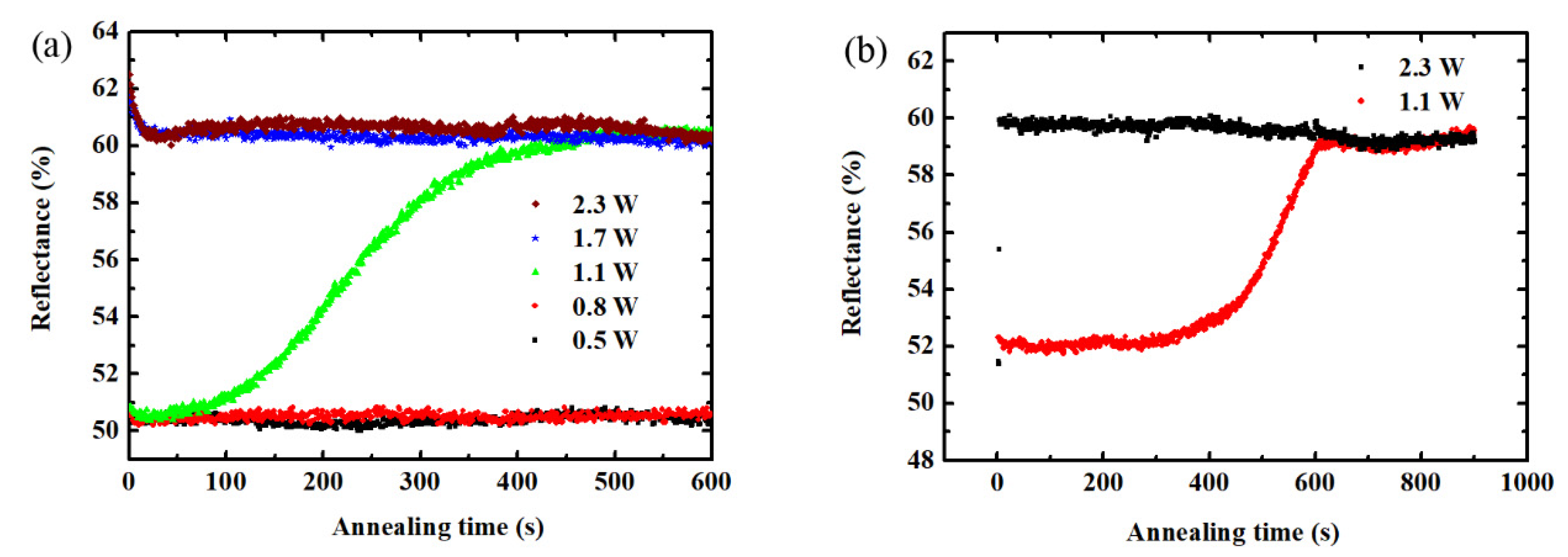
Section 2.2. The first study had a dual purpose: to estimate the power threshold required to trigger the crystallization and to determine if higher powers result in modifications to the reflectance of the layers and consequently their crystallization state. For this reason, the same zone on the thin film (thin film 1: TF1) was irradiated with increasing laser power. More specifically, the power for the irradiation ranged from 0.5 to 2.3 W with a step of 0.2–0.3 W, while a 10 min laser irradiation was performed for each power. This range of powers was employed because it was found to result in efficient annealing and allowed to avoid modification and damage to the layers, which has been found to arise for laser powers higher than 3.5 W. The reflectance as a function of the wavelength was recorded throughout the annealing procedure in the 500–1100 nm range, as described in
Section 2.2. In
Figure 1a, representative curves of the reflectance at 900 nm are represented as a function of the irradiation time for different annealing powers. This wavelength was arbitrarily chosen; similar behaviors were obtained for the other wavelengths in this range. No modification of the crystalline state was found during irradiation carried out by using laser powers lower than 1 W. However, when the sample was irradiated by 1.1 W, a gradual increase in reflectance was observed, as would be expected for a Sb
2Te
3 thin film passing from an amorphous to a crystalline state [
14]. A reflectance maximum was obtained about 7 min after starting the annealing. No further modification of the layer reflectance was observed after reaching this maximum; that is, for an annealing duration longer than 7 min. Additionally, when the same zone was irradiated with higher laser power (1.3–2.3 W), the reflectance remained the same, indicating that an optimal annealing had already been obtained using 1.1 W. It should be noted that for all the recorded curves, an initial decrease in reflectance was observed during the first seconds of laser annealing. This decrease, which occurred even at low power, was not attributed to a change of the crystalline state of the materials but to a modification in the reflectance as a function of the temperature of the Sb
2Te
3 sample, which our group had previously observed [
6].
It has to be noted that the optical response of a material (e.g., its reflectivity) is directly related to the motion of electrons in the conduction band and to the damping mechanisms (i.e., electron–electron and electron–phonon scattering) that transferred energy from the laser to the sample. In our case, we observed a temperature increase of around 200 °C in the first seconds of the laser annealing. Since both the motion of the electrons and the damping mechanisms depend on the temperature, the optical properties were modified due to variation in the sample temperature in this first phase, which explained the decrease of the reflectance during the first seconds of irradiation. Another annealing study was carried out to discover if faster crystallization than that obtained by 1.1 W laser power can be achieved by directly irradiating a Sb
2Te
3 sample with higher laser powers. A comparative study in this case was performed on two thin films using single laser power annealing for each film. In the first case, a 1.1 W laser power was chosen (thin film 2: TF2), while 2.3 W laser power was employed in the second (thin film 3: TF3). The results of this comparative study can be seen in
Figure 1b. Three different facts have to be highlighted. Firstly, in the case of the low power irradiation, a 10 min annealing was necessary. This duration is higher than that obtained for the previous irradiation (7 minutes, see
Figure 1a). This difference can be attributed to the fact that the sequence of crystallizations performed under low power, in the case of the study shown in
Figure 1a, did not result in a detectable crystallization change but rather accelerated the annealing that took place under 1.1 W. Moreover, in the direct annealing case using a 2.3 W laser (
Figure 1b), a very fast crystallization was obtained. Indeed, a 5 s annealing was sufficient to obtain a reflectance maximum, while no significant reflectance changes were observed for longer annealing durations. Finally, the initial decrease of the reflectance due to the temperature increase was not visible due to the fast increase in reflectance linked to the rapid crystallization, which masked the former, less-significant effect. As mentioned in
Section 2.2, the temperature of the sample was monitored by a thermal camera throughout the annealing. The maximum temperatures attained in the case of the TF2 and TF3 samples were 80 and 217 °C respectively.
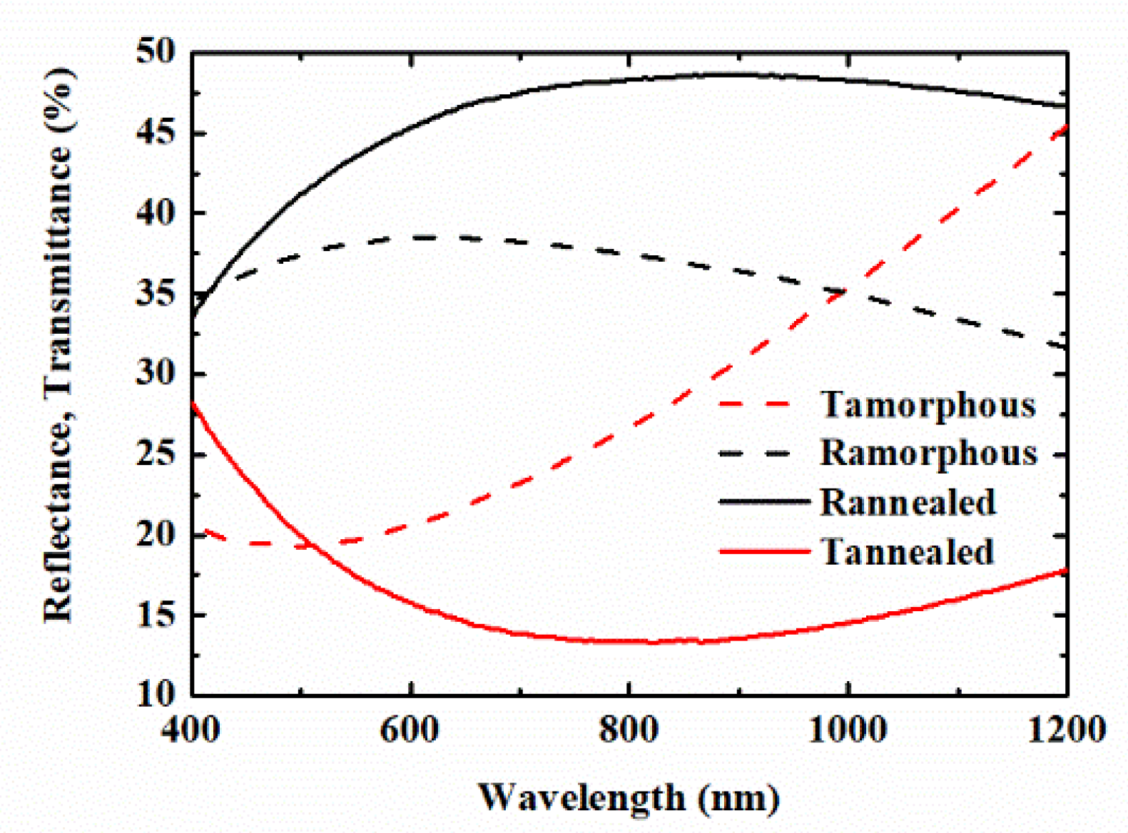
After the annealing, Vis-NIR spectrophotometric studies from 400 to 1200 nm were performed by a PerkinElmer Lambda 1050. Representative curves of the reflectance and transmittance of the annealed and amorphous zones of the TF3 sample can be seen in
Figure 2, and very similar spectra were recorded for the other samples. More specifically, the red curves correspond to the transmittance and the black to the reflectance. In the same figure, the dashed and continuous lines correspond to the amorphous and crystalline zones, respectively. The values obtained at 1030 nm were taken into account during the analysis of the nonlinear optical data. It should be noted that the reflectance value of the sample at 900 nm was different from that presented in
Figure 1 because of the different angles of incidence employed during the laser annealing and spectrophotometric studies.
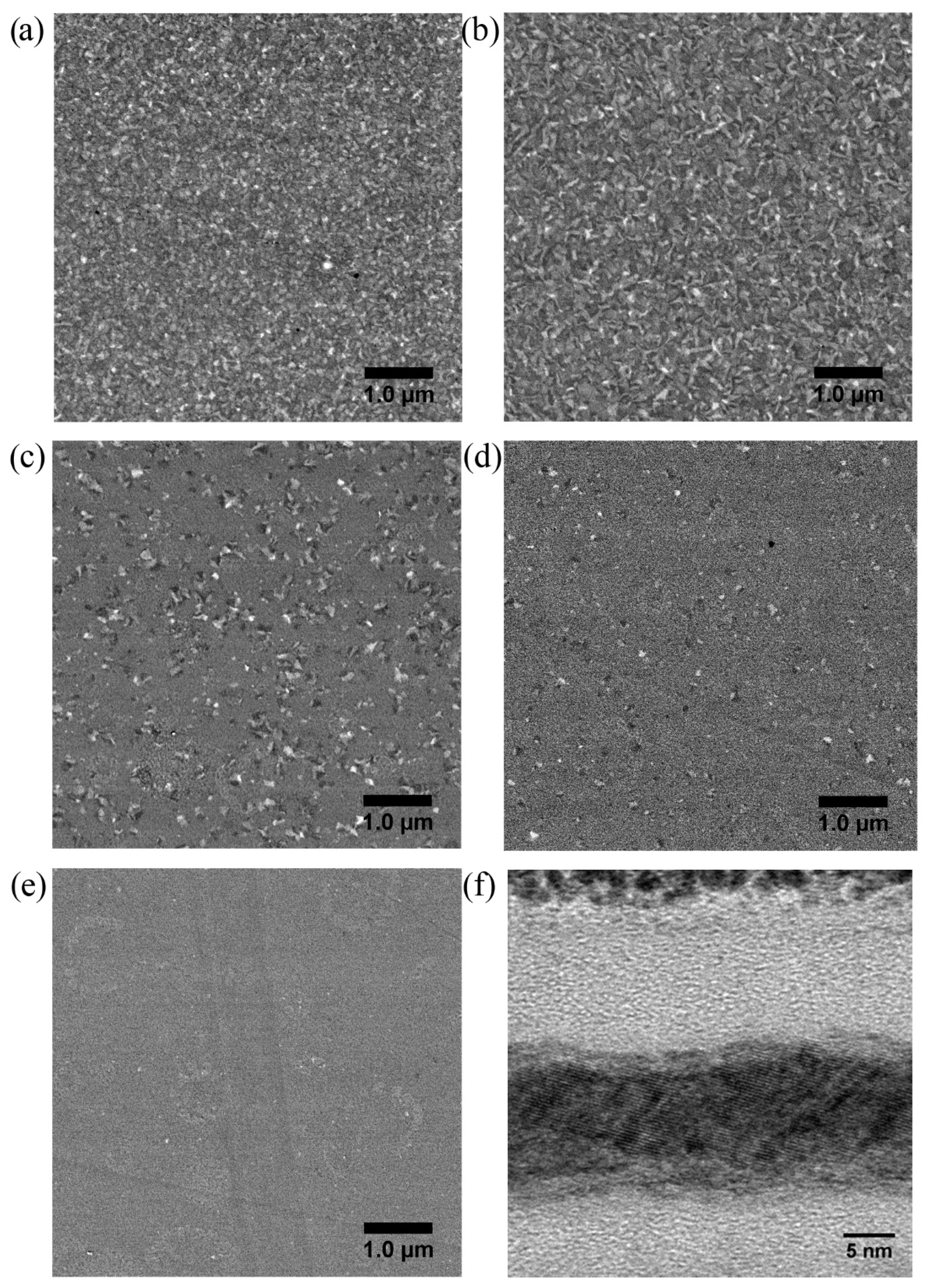
Scanning electron microscopy studies were additionally performed inside and outside the annealed zones. Many images were recorded for each sample at different positions in the crystallized zones. Representative results, obtained in the case of the TF1 film can be seen in
Figure 3. One can note a high density of crystals in the central part of the annealed zone (
Figure 3a).
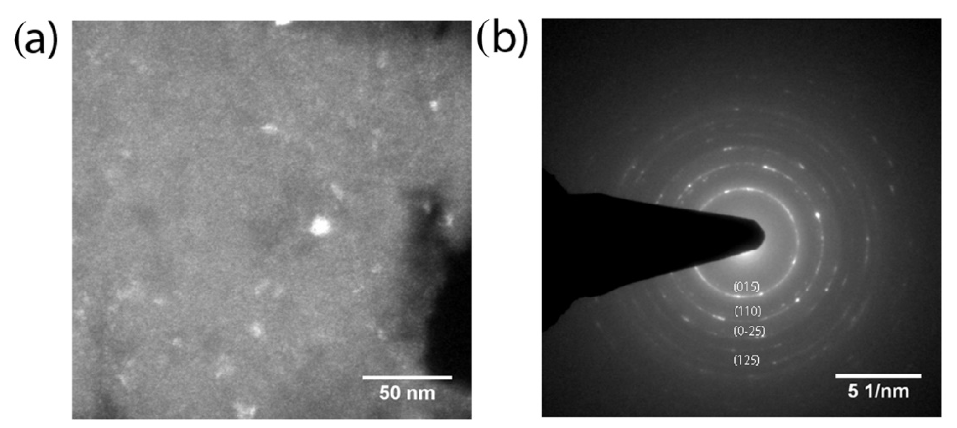
These grains of a size smaller than 30 nm were also observed on dark field TEM images (
Figure 4a). In addition, the diffraction pattern showed rings with distances coherent with the rhombohedral crystalline structure of the Sb
2Te
3 phase (
Figure 4b).
An HRTEM image observed on a cross-section of sample TF3 prepared by FIB revealed the presence of lattice fringes 0.321 nm distant (
Figure 3f), corresponding to (015) planes. This image also confirmed that the layer was well crystallized. The measured layer thickness is equal to 14 ± 2 nm. The difference between the thicknesses stated here for the annealed samples and those given in
Section 2.1 for the amorphous layers can be attributed to the crystallization, which resulted in slightly rough surfaces due to the transfer of matter during the annealing.
The shape of the crystals was found to be different a few millimeters away from the center, see for example an image obtained 2.3 mm away from the center in
Figure 3b. This shape difference resulted in a significant loss in nonlinear absorption, which is presented in the next paragraphs. Near the border of the crystallized zone (
Figure 3c,d), the crystal density was significantly reduced. Outside the annealed zone, no crystals were observed (
Figure 3e). The optical nonlinearities obtained near the border and outside the annealed zone were found to be negligible.
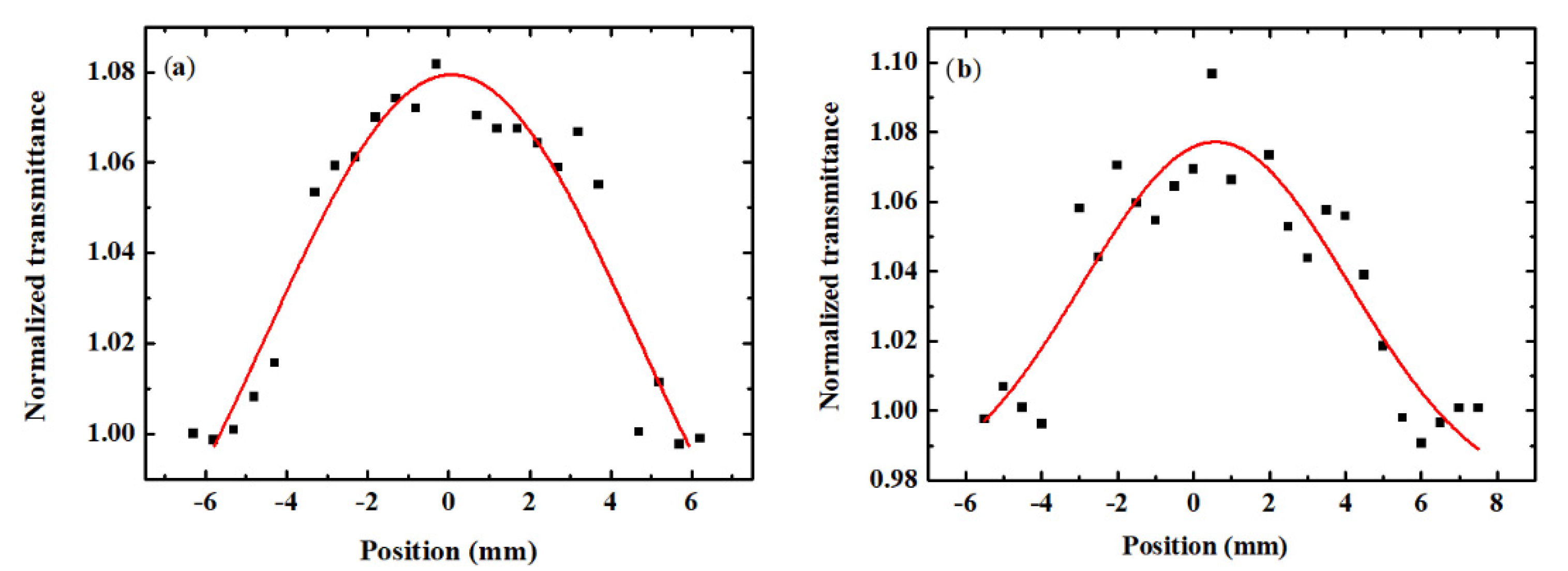
After the thin film layers were prepared and characterized, nonlinear optical studies were performed. The first study determined the nonlinear transmission inside the laser-crystallized zones of the samples, which had been scanned by a 40 μm diameter laser beam. For each position of the laser beam in the crystallized area, the following procedure was followed: Firstly, a weak laser intensity (0.04 GW/cm2) was used to determine the linear transmittance of the sample. An increase in transmission, while scanning the sample from the center to the edge of the crystallized area, was observed and was attributed to the Gaussian spatial profile of the laser beam used for the annealing. This variation in transmission was taken into account during the next step of the analysis.
Using a higher intensity (3 GW/cm
2), the saturable absorption character of the samples was activated, resulting in an increase in the transmission of the Sb
2Te
3 layers. The transmission of the sample at the high intensity regime divided by the transmission obtained at the low intensity regime provided the normalized transmittance, which is presented in
Figure 5a,b for the samples TF1 and TF3, respectively. As can be seen in these figures, the optical nonlinearities were significant in a zone having a diameter of about 1 cm, which matches the size of the crystallized zone. Outside this zone, the optical nonlinearities were found to be negligible, so the normalized transmittance was equal to unity. It can be seen that the maximum transmittances were similar for the samples TF1 and TF3: about 1.08. The average nonlinear absorption coefficient (β) of the central part of the annealed zones was calculated based on the measured nonlinear transmissions and using the expressions shown in
Section 2.4. It was found to be −1.7 × 10
−6 and −1.6 × 10
−6 m/W for thin films TF1 and TF3, respectively. In the case of the TF2 sample, the lower power (1.1 instead of 2.3 W) resulted in a smaller crystallized zone (radius less than 0.2 cm) which would render a study imprecise. By comparing these results with the SEM images in
Figure 4, it was noted that the shape of the crystals and their density had a high impact on the optical nonlinearities. Indeed, near the center of the annealed zone, a high saturable absorption was obtained, but it gradually decreased as the laser beam moved towards the border of this zone.
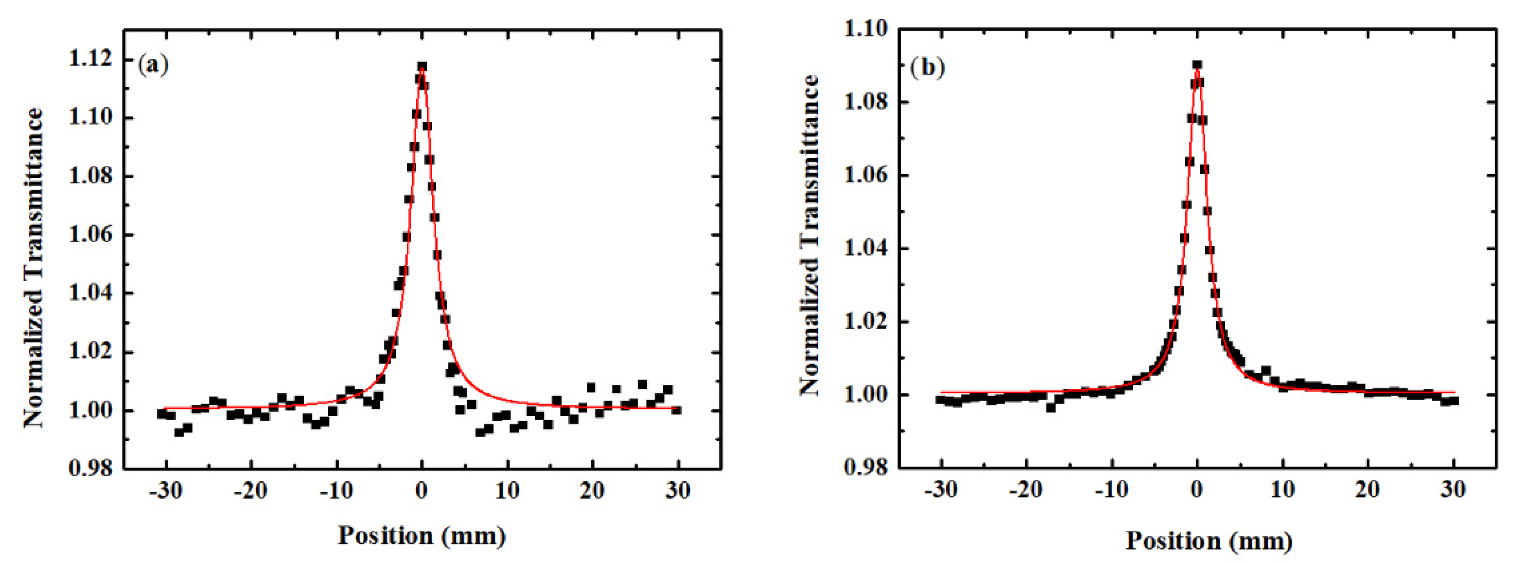
To provide a more precise determination of the nonlinear absorption coefficients of the annealed thin films, Z-scan studies were performed in the center of the crystallized areas. A very good alignment of the experimental setup was necessary to make sure that the sample was always at normal incidence. In this way, the laser beam irradiated the same area of the sample, while moving along the
Z-axis of the setup. Two representative open aperture Z-scan curves are shown in
Figure 6a,b for thin films TF1 and TF3, employing 4.3 and 3.0 GW/cm
2, respectively. In both cases, a transmission peak was acquired, revealing the saturable absorption behavior of the investigated thin films. The nonlinear absorption coefficients were determined by fitting the results with the models presented in
Section 2.4 and found to be −2.3 × 10
−6 m/W for both TF1 and TF3.
These values were in good accordance with those determined by the nonlinear transmission study. The difference between the values obtained from the two studies can be attributed to the fact that during a Z-scan study the same spot on the sample was irradiated throughout the scan, while in the case of the nonlinear transmission analysis, the β value was determined by averaging over many different measurements obtained at different sample positions in the central part of the crystallized zone. The inhomogeneities of the crystalline structure due to the Gaussian beam profile employed for the annealing gave rise to this difference. The values obtained were also in very good agreement with previous results reported by our group. In reference [
7], we performed a thickness-dependent nonlinear optical study of Sb
2Te
3 thin films. The nonlinear absorption coefficient for thin films of the same thickness (10 nm) was −1.5 × 10
−6 m/W. This value was slightly lower than those obtained in this work, which can be attributed to the different annealing methods employed. In our previous work, oven annealing was employed, while here it was a laser annealing. However, the setup that was employed (Z-scan) and the experimental conditions were identical between the two works, so a direct comparison of the results is feasible. A detailed comparison of the optical nonlinearities of the Sb
2Te
3 thin films prepared by our group and the results of other scientific groups on highly efficient photonic materials had been previously presented (see reference [
6] and Table 1 therein).


 ,
, 


