
Chip-Scale Quantum Emitters


Photonics and Quantum Technologies Research School, Nuclear Science and Technology Research Institute, Tehran 11155-3486, Iran
Quantum Rep. 2021, 3(4), 615-642; https://doi.org/10.3390/quantum3040039
Submission received: 10 July 2021
/
Revised: 7 September 2021
/
Accepted: 8 September 2021
/
Published: 29 September 2021
Abstract
:Integration of chip-scale quantum technology was the main aim of this study. First, the recent progress on silicon-based photonic integrated circuits is surveyed, and then it is shown that silicon integrated quantum photonics can be considered a compelling platform for the future of quantum technologies. Among subsections of quantum technology, quantum emitters were selected as the object, and different quantum emitters such as quantum dots, 2D materials, and carbon nanotubes are introduced. Later on, the most recent progress is highlighted to provide an extensive overview of the development of chip-scale quantum emitters. It seems that the next step towards the practical application of quantum emitters is to generate position-controlled quantum light sources. Among developed processes, it can be recognized that droplet–epitaxial QD growth has a promising future for the preparation of chip-scale quantum emitters.
1. Introduction
Today, it is easily understandable that the development of integration technology has led to great progress in the field of device miniaturization, and great innovations have been achieved in the fabrication of advanced devices. The first step in miniaturization of devices was the development of integrated circuits [1], the first of which was created by Texas Instruments, often considered to be one of the most important inventions in microelectronics [2]. The first integrated circuit was built from a single piece of germanium and a phase-shift oscillator that used transistors, resistors, and capacitor elements [3]. Today, billions of transistors can be squeezed onto a single microprocessor chip, leading to continuous increases in computing speed and data processing performance. However, after several decades of attempts to improve the performance of computers based on complementary metal–oxide–semiconductor (CMOS) technologies, it was recognized that the limit of this technology was approaching [4,5]. Moreover, it has been pointed out that the power-consuming signal transportation and resistance–capacitance (RC) delay becomes increasingly problematic as the bit rate increases [6]. To overcome the bottleneck of complementary metal–oxide–semiconductor (CMOS) technology, photonic integrated circuits or planar lightwave circuits are proposed, in which optical components are combined to fulfill some more or less complex functions [7]. In comparison with CMOS technology, optical circuits do not suffer from the same barriers, and are restricted only by their intrinsically low nonlinearity and poor functionality [8]. Due to the replacement of electricity with light in the planar lightwave circuits, it was expected that the technological barriers in the fabrication of advanced integrated circuits could be satisfied using aligned submicron optical components [9]. In the early years of the development of integrated optical technology, it was found that this approach has the potential to revolutionize our future computation systems as a result of dramatic increases in the speed of computing and signal processing.
Consequently, many attempts have been made to develop highly functional optical devices with the potential for integration in wafer-scale integrated optical packages [10]. Nevertheless, the manufacturing challenges of architected photonics chips for high-speed and energy-efficient optical integration platforms have persisted [11]. Therefore, co-integration of electronics and optics was previously proposed on the same chip, fabricated with a well-mastered microelectronics fabrication process which can provide high-functionality and high-performance integrated devices [12]. In this way, technological requirements such as bandwidth and power efficiency present a need to consider alternative interconnected technologies beyond electrical interconnections [13]. In addition, the chip-to-chip interconnections in multisocket computational units present the need to enhance point-to-point optical connectivity [14]. From a technological standpoint, it has become clear that silicon photonics (SiP) can be considered an ideal candidate for answering these needs [15,16,17,18]. By using chip-scale electronic–photonic devices based on silicon photonic circuits, some limitations have been overcome, and the ability to transmit increasingly higher data rates has been achieved [15]. Furthermore, as a result of the ability to build photonic–electronic integrated circuits on the mature CMOS industry platform, some of the required specifications—including high bandwidth, high energy efficiency, low attenuation, and parallelization through wavelength division multiplexing (WDM)—are now becoming available [15].
The predominant driving forces for the commercialization of silicon photonics originate from an explosive increase in the volume of global network and data center traffic [19]. Today, video streaming, social networking, and cloud computing require an interconnection scheme with low cost, high energy efficiency, and high bandwidth capacity [19]. Since the computing in data centers usually originates from—and is terminated by—the electrical domain, the interconnection between electronic systems and applied silicon photonics, therefore, requires an interface. Additionally, as a crucial factor in the design of photonic integrated circuits, the electrical signals for modulators originating from photodiodes need to be amplified in order to provide sufficient impact on the transceiver bandwidth and energy efficiency [20,21]. Therefore, to achieve improved scalability and lower costs of silicon photonic integrated circuits (PICs), the modern CMOS packaging techniques that were originally developed for the cell phone and IT industries are being applied [22]. Figure 1 shows the gradual evolution of datacom transceivers through five generations of technology [22]. In parallel with the common low-cost Si substrate, the fabrication of integrated silicon photonic devices can benefit from scaling up to 300 mm diameter wafers using standard CMOS facilities [22].
In addition, the integration of photonic elements such as lasers, modulators, photodetectors, and other passive devices has been exploited to complete certain functions in Si photonics integrated circuits (PICs). Besides the low-loss waveguides that are also interconnected with other elements, arrayed-waveguide gratings (AWGs), Mach–Zehnder interferometers (MZIs), and phase tuners can be integrated in a Si PIC [22]. To satisfy the specifications of a single Si PIC for application in different areas, including high-speed transceivers, LIDAR, optical computing, and quantum photonics, an increased number of elements on a single, large-scale Si PIC are necessary to provide high device yield. To improve the optical signal quality in a large-scale PIC, a balance between the number of channels, the optical losses, and amplification values must be reached. Evolution of the number of photonic devices integrated on a single waveguide, platforms including monolithic InP with integrated lasers, monolithic Si without integrated lasers, and Si substrate with integrated lasers are summarized in Figure 2 [22]. Figure 3 shows the progress over the past four years and the projection for the next two years. With the advent of quantum technology as one of several emerging technologies in the last decade, the idea of control and manipulation of physical objects at the quantum level has been considerably strengthened. Now, quantum technology’s aim is to successfully make quantum devices by the use of quantum physics.
Therefore, quantum technology can affect the way we live due to its ability to provide fascinating advances in both technology and fundamental science areas. The most important aim of this technology is to pave the way for smaller, faster, and more flexible electronics than ever before. Only during a few years, the development of quantum technology was realized due to its potential for commercial applications and strategic sectors and transferred from “blue sky” science to a field of technology rapidly [22]. For instance, quantum computing as a feature of quantum technology—processing a sufficient quantum volume with advantages in real-world applications—can be employed to solve cryptanalytic or machine learning algorithm problems. It does not mean that a quantum computer made with mechanisms and methods of quantum technology and the precision, accuracy, speed, and endurance factors of the quantum computer are determined to describe its performance. It seems that high-performance computing with quantum computers can be obtained by the development of room temperature superconducting materials. Many researchers believe that the use of quantum technology in integrated silicon circuits can lead to quality improvement of silicon-based photonics, and new devices are going to be built based on this integration approach. For instance, using the integration of quantum technology in silicon photonics, devices can be built to meet our technological needs in the field of communications, information, and data processing [23]. Regarding the challenges that need to be tackled for the maturation and scaling up of quantum photonic integrated circuits (PICs), major areas such as components, platforms, and integration processes must be developed. For example, several quantum elements such as grating couplers, waveguides, phase shifters, cavities, resonators, single photon sources, light emitting diodes, and detectors need to be matured and their operation optimized for a selected wavelength range. In addition, for scalable quantum operation, the insertion loss of quantum elements must be drastically reduced and their ability for integration into a standardized platform must be improved. In regard to the integration challenges, it was found that silicon integrated quantum photonics can be considered a promising approach to generate and manipulate entangled states of light on-chip scale and realize quantum integrated circuits. Among quantum technology subsections, quantum emitters were selected as the case of study. With this approach, the newest findings and progress obtained in recent years are highlighted to provide an extensive overview of recent developments in quantum emitters.
2. Quantum Emitters
On the basis of lab-scale experimental results for the preparation, manipulation, and read out of quantum states from a modest number of quantum bits (qubits), we need to use different benchtop components, including tunable and narrow-line width lasers and optical elements such as lenses, wave plates, and prisms. Therefore, to realize photonic quantum systems, quantum scientists and engineers need to solve the integration challenges of quantum system components. Analogous to integrated circuit chips, the quantum circuits need to integrate thousands or millions of components and quantum elements on one chip. These components must provide the required functionality, high performance, and stability. Consequently, novel design architectures and fabrication techniques with the ability to integrate the quantum elements into chip-scale electronics are essential [24]. To exploit the quantum circuit technology, the implementation of a scalable architecture must be established beyond the realm of ‘mere’ engineering and, therefore, a transformative approach is required [25]. For example, superconducting qubits and superconducting nanowire single-photon detectors operate in an RF regime [25]. Due to the power dissipation, footprint, limited frequency, and accuracy of the CMOS standard devices used for control and readout, the scale-up in the size of this kind of single-photon detector is limited when we attempt to achieve the required performances in real-world applications [25,26]. Tasker et al. believed that the classical interface hardware for integrated quantum photonics is still being implemented with large-footprint discrete electronics that limit device scalability and performance. Therefore, silicon quantum photonics is not able to be integrated with monolithic complementary metal–oxide–semiconductor (CMOS) electronics [27]. In Figure 4, key milestones for integrated quantum photonics in the past decade are shown [28]. As can be found from this figure, in 2008, the fabricated circuit contained a few components. However, a quantum device with more than 650 components was formed in 2018. The capability of these devices changed from enabling two-photon quantum interference to two-qubit operations. This rapid progression triggers enabling discoveries in foundational quantum mechanics, computing, communications, and metrology [28]. Similar to the integration and complexity level of conventional PICs, the integration and complexity level of QPICs need to be developed significantly. Today, the most advanced PICs comprise ~5 × 10³ components, which can be considered as the upper limit for what is currently achievable for QPIC scalability with existing fabrication and packaging technologies [28].
As mentioned above, since integrated quantum photonics (IQP) is a compelling platform for the future of quantum technologies, many attempts have been made to overcome the integration challenges at the chip scale. This technology originated from quantum information theory and it has become a powerful research methods toolbox for researchers from numerous fields to find answers to many of their scientific questions today. To date, various quantum compounds have been exploited to promote the realization of quantum integration technology. Quantum compounds that have been developed for quantum technology integration consist of superconducting circuits, nonlinear waveguides, ultracold atoms, trapped ions, cavities, solid-state spins, and emitters [29]. Quantum emitters are one of the most important quantum compounds that are needed to be prepared in the chip scale. Consequently, the exploitation of wafer-scale fabricated single-photon sources is highly notable. As has been highlighted, a large number of identical single photons are required for harnessing the power of integrated quantum photonics IQP on the chip scale. Accordingly, different types of quantum emitters with the ability of integration on the chip scale were introduced. Usually, quantum emitters include parametric photon-pair sources and single-photon sources (SPSs) [29]. Among them, single-photon sources play an important role in the advancement of quantum technology, which means that installation of single-photon sources (SPSs) on a chip that can deterministically emit indistinguishable single photons is very critical for the scaling operation of single-photon-based quantum photonic integrated circuits (QPICs). In Figure 5, the SPS timeline for developing physical systems and materials is shown. To provide the right impression of integrated quantum chips, a sample of the configured integrated quantum compounds is shown in Figure 6 [29]. In Figure 6a, the first IQP circuit for CNOT entangling operation in silica-on-insulator waveguides is illustrated. The control and target qubits are represented by Ci and Ti (i = 0, 1) in this circuit. VA and VB are ancilla qubits. The cladding layers of regions I and III are presented in the bottom left panel, and II is the silica core layer [29]. In Figure 6b, a quantum circuit in silica, prepared by laser writing, is shown. Complex three-dimensional integration can be produced using the quantum circuit. Pure and identical photons can be generated by the integrated spontaneous four-wave mixing (SFWM) SPS in Si photonic waveguides or microresonators, which are shown in Figure 6c.
Figure 6d shows an integrated spontaneous parametric down-conversion (SPDC) SPS in GaAs waveguides which sustains two different types of eigenmodes meeting the phase matching condition [29].
In this section, W and D indicate the width and height of the waveguide, respectively. Figure 6e presents a semiconductor InGaAs/GaAs quantum dot (QD) SPS that can efficiently emit pure single photons from a single dot embedded in a micropillar. An integrated photon-number-resolving (PNR) detector with a transition-edge sensor (TES) that is evanescently coupled to silica waveguides can be observed in Figure 6f. An integrated superconducting nanowire single-photon detector (SNSPD) atop a Si waveguide that can absorb and detect photons with >90% efficiency is shown in Figure 6g [29]. An integration of a QD source with two SNSPDs in the GaAs photonic crystal waveguide system that enables the on-chip detection of QD luminescence and an integration of four SFWM single-photon sources with re-programmable quantum photonic circuits in Si allows the on-chip preparation, manipulation, and measurement of photonic qubits T and B. Here, Ri (i = x, y, z) are rotation operators implemented by the phase shifters (θ, φ) and can fine in Figure 6h,i [29]. An integration of Si photonic circuits with SNSPDs (A1, A2, and B1,2) by using the micrometer-scale flip-chip process that allows on-chip detection of nonclassical light can be found in Figure 6j. An important point that can be recognized from this figure is that single-photon sources play a critical role in the development of quantum technology. As can be found from Figure 5, single-photon sources can be classified into different types, including 2D materials, quantum dots, thin films, carbon nanotubes, and oxides. In the following section, some of these and their quantum emitters will be presented.
2.1. Quantum Dots
The potential of QD SPSs for deterministic generation of single photons was previously established using self-assembled InGaAs/GaAs QD SPSs, which show the best performance [29]. At present, the highest all-round SPE performance was achieved using self-assembled InAs/GaAs QDs. Using a resonant excitation technique, near-optimal single-photon emission from a single QD was demonstrated [29]. In addition, single or several QD sample(s) have been employed to achieve: single-photon purity of more than 99%, extraction efficiency of more than 65%, and photon indistinguishability close to 99% [29]. Over the last decade, several developed methods, such as coupling QDs to micropillars, nanowire antennas, microlenses, or circular Bragg grating, have been employed to increase photon extraction efficiency above 50% [29]. In addition, the production of many-photon quantum states can be achieved by time-delaying emissions from a single QD result. A key challenge for maintaining a high rate of multiphoton state generation and overcoming the loss of the overall rate is the reproducible growth of multiple identical dot samples. The emission wavelength of QDs can be engineered in the telecom-wavelength region, in which the transparency of silicon is available, and noticeable progress towards infrared emitters has also been obtained, which indeed make a better interface with telecom systems [24,29]. Recently, it was demonstrated that InAs/InP SPEs can emit in the telecom spectrum (1550 nm) in a nanophotonic cavity [31]. To find a way for integration with existing fiber architectures, the carrier frequency of quantum states of NIR photons generated from a bright quantum dot was also manipulated to provide telecommunication C-band emission [32]. In a difference-frequency generation process, the frequency of single photons was converted from 942 nm to 1550 nm using a custom-built, tunable 2400 nm seed laser. The achieved end-to-end conversion efficiency in their experiments was 35%, which demonstrated that count rates approaching 1 MHz at 1550 nm with g(2)(0) = 0:043(1), and Hong–Ou–Mandel (HOM) visibilities of 60%, were achieved. It was believed that the presented scheme is preferable to quantum dot sources directly emitting at telecom wavelengths for fiber-based quantum networking [32]. Holewa et al. [33] explained the practical use of QDs in fiber-based quantum communication prepared by metal organic vapor-phase epitaxy-grown InGaAs/GaAs QDs emitting in the telecom O-band at 1.3 μm. At elevated temperatures up to at least 80 K, it was observed that the excitation of trapped holes in the vicinity of a QD leads to the formation of trion states with enhanced emissions [33]. They concluded that the main source of luminescence quenching is related to the promotion of holes to higher states in the valence band. The purity of up to 50 K for single-photon emission was recorded using photon autocorrelation measurements [33]. Another advance in photonic quantum technology was obtained by localization of single-photon sources in an array of 28 × 28 mesas with site-controlled InGaAs quantum dots [34]. In the experiments, the buried stressor approach was used to achieve the site-selective growth of quantum dots. The nucleation site in the center of each mesa was provided by an oxide aperture. The quantum nature of emission in terms of high single-photon purity and photon indistinguishability was measured and values of g(2)(0) = 0.026 ± 0.026 and a post-selected two-photon interference visibility V= (87.1 ± 9.7)% with an associated coherence time of τc = (194 ± 7) ps were obtained [34]. Recently, planarized SPS arrays based on a unique class of shape-controlled single quantum dots (SQDs) synthesized on a mesa top (dubbed MTSQDs) were reported by Zhang et al. [35]. To enable the spatially selective growth, they used substrate-encoded size-reducing epitaxy (SESRE) on spatially regular arrays of patterned GaAs (001) while square nanomesas with edges along <100> were chosen [35]. In this study, the planarizing overgrowth process over arrays of InGaAs SQDs largely maintains the SQDs’ high single-photon emission purity (>98%) and spectral uniformities (~5 nm) are demonstrated [35]. To demonstrate highly efficient quantum light sources in visible frequencies for photonic quantum technologies, an embedded droplet-epitaxial QD in an L3 type photonic crystal nanocavity was developed to introduce a bright single-photon source [36]. The prepared source showed an extraction efficiency of 23.6%, single-photon purity of 96%, and a polarization degree of 82.7% [36]. Recently, wafer-scale low-density InAs/GaAs quantum dots (QDs) for a single-photon emitter on a three-inch wafer by precisely controlling the growth parameters were successfully achieved [37]. An excellent optoelectronic property with a linewidth of 3 ± 0.08 GHz, second-order correlation factor of g2(τ) = 0.0322 ± 0.0023, and exciton lifetime of 323 ps under two-photon resonant excitation were reported by Huang and co-workers [37]. Schuck and co-workers [38] presented a novel semiconductor single-photon source based on tensile-strained (111)-oriented GaAs/InAlAs quantum dots (QDs) exhibiting ultrasmall exciton fine-structure splitting (FSS) of ≤8 μeV. Due to the possibility of frequency matching between a rubidium-based photon memory and embedded GaAs QDs in an AlGaAs matrix, they have potentially improved electron spin coherence compared to the widely used InGaAs quantum dots [39]. To provide their charge stability and optical linewidths, GaAs quantum dots were embedded into a p-i-n (PIN) diode that operated at low temperatures and demonstrated ultralow noise behavior. The control of charge was performed via Coulomb blockade and no blinking was observed. The linewidth of the established platform is close to lifetime-limited linewidths. High-fidelity optical electron-spin initialization and long electron-spin lifetimes for these quantum dots were observed [39]. Hu et al. [40] explained the direct two-photon excitation effect on the photoluminescence of self-assembled InAs/GaAs quantum dots grown by molecular beam epitaxy. The direct two-photon absorption in the dots was unambiguously confirmed by the quadratic power law dependence of the photoluminescence intensity. Another reason for the direct two-photon absorption was distinguished by the ground-state resonant peak of quantum dots appearing in the photoluminescence excitation spectrum [40]. The photogenerated carrier dynamics in the quantum dot-wetting layer-GaAs system was described using a three-level rate equation model. In this approach, the use of two-photon excitation leads to higher-order power law dependence of photoluminescence intensity on both the GaAs substrate and the wetting layer [40]. Holewa and co-workers [41] used a ripening step in molecular beam epitaxial growth of InAs quantum dots (QDs) embedded in an (In,Al,Ga)As barrier lattice matched to InP(001) that led to the growth of in-plane symmetric QDs. The spectrally broad emission in the range of 1.4–2.0 μm resulted from the low surface density of highly symmetric QDs [41]. A nearly dispersionless measured value of 1.3 ± 0.3 ns for the lifetime of spectrally broad emissions was found. Finally, it has been specified that the role of a carrier reservoir was played by the localized states in the wetting layer. It was determined that the hole escape to the (In,Al,Ga)As barrier may be due to a primary PL quenching mechanism in these QDs [41]. Seravalli and Sacconi [42] provided a review of quantum dot (QD) material systems, including InAs QDs grown on InP, metamorphic InAs/InGaAs QDs grown on GaAs, InAs/GaSb QDs grown on Si, and InAsN QDs grown on GaAs, that allow us to obtain light emission in the telecom C-band at 1.55 μm. Numerical simulations based on envelope function approximation were used to calculate the strain-dependent energy band profiles. The associated confined energy levels were investigated to provide a quantitative comparison of different material systems [42]. In their approach, the eigenfunctions and the optical matrix elements were also derived to confine the states of the systems. To optimize the structural engineering aimed at single-photon emission in the telecom C-band region, some general conclusions on the strengths and weaknesses of each QD material system have been drawn [42]. Arakawa and Holmes [43] presented a broad-spectrum overview of the QD-based single photon emitters developed to date, from the telecommunication bands in the IR to the deep UV range. They concluded that the majority of advances in high-quality single-photon emitters have been made in the infrared range using III-As or III-P QDs [43]. They believed that all experiments on photon indistinguishability have been performed using III-arsenide QDs emitting in the vicinity of 900 nm which is due to the well-established growth and sample processing techniques [43]. Their studies confirmed that high-temperature operation is needed to record the emission of QDs in the visible and UV wavelength regions. Due to the operation at high-temperature and large phonon-broadening, the emission coherency will reduce significantly. Even in the presence of such phonon-related linewidth broadening and the spectral isolation of individual emission peaks resulted from large biexciton binding energies, the high-temperature operation of these devices is possible [43]. A selection of emitter properties separated by material system is presented in Table 1. Arakawa and Holmes pointed out that the majority of studies on QDs operating in these wavelength regions are also on the test level. Consequently, different kinds of QDs with the designed properties and with possible applications in the visible and UV wavelength regions must be developed and their limits must be overcome. In commercialized quantum communication, the quantum information must be transferred over long distances. However, to avoid the loss of data over a long communication distance, the quantum repeater is needed to subdivide the transmission line into several segments interconnected by entanglement distribution via Bell-state measurements to overcome inherent channel losses [44]. Consequently, high indistinguishability within each repeater node is necessary. This can be supplied by single-photon sources demonstrating evidence of strong multiphoton suppression. To build and make a repeater with a successful operation, the matching of spectral features between quantum light sources must be achieved [44]. Recently, a spectrally tunable single-photon source was developed that can emit in the telecom O-band [44]. Accordingly, a coupling between a piezoelectric actuator via gold thermocompression bonding and a thin membrane of GaAs embedding InGaAs quantum dots (QDs) was used to produce a tunable single-photon source [44].
Here, the role of electrical connection was played by a thin gold layer—which acts as a strain transfer structure—and broadband backside mirror for the QD micromesa that was prepared by in situ electron-beam lithography [44]. Experimental results showed that the multiphoton suppression had not been influenced by spectral tuning [44]. Besides the development in the preparation of advanced materials such as the QD-based single-photon emitter employed for experimental demonstration of quantum technologies, the improvement in fabrication techniques also continued. For example, to achieve cavity mode resonance with a great enhancement of QD photoluminescence (PL) intensity, a precise calibration process of an Al0.9Ga0.1As/GaAs DBR micropillar cavity, which matched the single InAs/GaAs quantum dot (QD) exciton emission, was proposed [45]. Under a weak coupling regime, the light–matter interaction of single QDs in a DBR micropillar cavity (Q∼3800) was investigated by temperature-tuned PL spectra. In this study, a value of g(2)(0) = 0.070 was demonstrated using the second-order autocorrelation measurement and highly pure single-photon emission at high count rates was indicated by the estimated net count rate before the first objective lens was reached (1.6 × 10⁷ counts/s) under continuous wave excitation [45]. A heterogeneous photonic integration platform was developed, allowing direct integration of GaAs waveguides and cavities containing self-assembled InAs/GaAs quantum dots that provide such capabilities in a scalable on-chip implementation [45]. In their experiments, a highly efficient optical interface between Si3N4 waveguides and single quantum dots in GaAs geometries was achieved which included quantum dot radiative rate enhancement in microcavities, and a path for reaching the nonperturbative strong-coupling regime [45]. Davanco et al. [46] indicated that robust implementation of single-photon sources can be achieved through the use of systems that provide both strong light–matter interactions and a low-loss interface between emitters and optical fields (Figure 7). Uppu et al. [47] reported a coherent and stable single-photon source that simultaneously achieves high purity (g(2)(0) = 0.020 ± 0.005), high indistinguishability- (V = 96 ± 2%), and >80% coupling efficiency with the waveguide. Such a ‘plug-and-play’ single-photon source can be integrated with on-chip optical networks implementing photonic quantum processors (Figure 8). As can be seen from the figure, the taper section is responsible for the collection and guidance of the squeezed emission out of the waveguide. The fundamental mode is reflected by a mirror prepared from a photonic crystal and, therefore, the directional out-coupling of the QD signal becomes available. The excitation and collection spots are highlighted with red and green spots. The fundamental and first-order modes of the waveguide are excited by a Y-splitter.
The transmission of first-order mode into the emitter section was selectively performed by the photonic crystal. To suppress the pump laser, a waveguide taper and two 90° bends were coupled with the pump laser filter. The bottom-left grating is used to align in-coupling of the laser beam by monitoring the reflected signal from the photonic crystal [47]. Another on-chip waveguide-coupled single-photon source was proposed by Jiang et al. [48], in which the waveguide was directly made by a quantum dot membrane (Figure 9). Grating output couplers are made at both ends of the waveguide to scatter light out of the on-chip waveguide plane into the detection apparatus [47]. The second-order correlation function g(2)(τ) measurements were performed using a Hanbury Brown and Twiss interferometer to indicate the photon statistics of the on-chip photon source. The obtained results showed an on-chip single-photon source that is easily implemented and easily integrated into quantum photonic circuits [48].
As mentioned before, the embedding of self-assembled quantum dots (QDs) at predefined positions in nanophotonic structures leads to an architecturally advanced and complex quantum-photonic platform. Pergonaloto et al. [49] showed that the position of QDs in nanophotonic waveguides relative to a predefined global reference frame can become deterministically distinguishable using microphotoluminescence (μPL) spectroscopy. They indicated that electrical or thermal tuning of QDs can, generally, be employed to compensate fabrication-induced spectral shifts [49]. Due to the fabrication process, it was demonstrated that the emission frequency at vanishing electric fields of different QD charge states can be varied [49]. The polarizability and the permanent dipole moment at vanishing electric fields of different QD charge states can also be affected by the fabrication process. They, then, concluded that the integration of QDs into nanophotonic waveguides can be achieved by their approach. In Figure 10, the epitaxial growth of QDs under a prelocalization protocol is shown. In part I of this figure, a false-color SEM of the GaAs membrane with embedded InAs QDs can be found.
Part II shows how the alignment mask is imaged and where the crosses are located, and part III indicates how the QD photoluminescence is pictured and spatially correlated with the cross positions. A close-up image of the emission pattern of a single QD is shown in IV. Progress was also made in the quantum integration platform by using the mechanical strain engineering of low-dimensional semiconductors. It is well known that the unpredictable transition energies of different QDs can be accounted for using randomness in strain, shape, and composition in semiconductors [50]. One of the powerful methods for reshaping the electronic states of semiconductors is strain engineering that can advance the development of all-solid-state low-dimensional semiconductor-based single- and entangled-photon sources with well-defined energies. The recent progress of employing a mechanical strain field to control the electronic states and optical properties of low-dimensional semiconductors is reviewed by Tao et al. [50]. They provided a comprehensive summary of diverse strain engineered devices for engineering the exciton binding energy, the coherent coupling of electronic states, and the optical properties of low-dimensional semiconductors including single and entangled photons. In addition, a discussion of the prospects and challenges of deploying the strain engineering technique for future scalable quantum networks and photonic quantum circuits was also presented. Yang and co-workers [51] emphasized that inability to grow perfectly identical quantum dots with ideal optical properties necessitates the application of post-growth tuning techniques via, e.g., temperature, electric, magnetic, or strain fields. They showed that the wavelength of single photons and entangled photon pairs emitted by InGaAs/GaAs quantum dots can be reversibly tuned using piezoelectric crystals such as PMN-PT [51]. For electrical triggering and tuning of the wavelength or the exciton’s fine structure, they used quantum light-emitting diodes. Furthermore, the frequency even feedback, which is verified by two-photon interference with photons from two stabilized sources, was employed to compensate the wavelength drift caused by piezo creep and also to ensure the indistinguishability of photons [51]. Nevertheless, by performing many attempts to prepare a GaAs quantum dot single-photon source on the chip scale, considerable progress was also made in the preparation of III-nitride QDs that can even operate at room temperature. However, a reliable SPE platform with a high signal to noise ratio and relatively low g(2)(0) must be achieved by the growth of high-quality material with a higher emission energy of ~3 eV. Due to the large exciton binding energies of III-nitride semiconductor quantum dots (QDs), they are promising candidates for single-photon emission at noncryogenic temperatures [52].
It has been reported that GaN QD single-photon emitters can operate at 300 K and their performance for the emission of single photons depends on the balance between the emission line width and the biexciton binding energy [52]. It has been shown that when using GaN QDs embedded in a planar AlN layer, grown on silicon, the brightness and single-photon purity can be adjusted to improve the performance metrics [52]. Authors have described that the large exciton binding energies lead to high brightness and, by the spectral overlap with the biexcitonic emission, this can be used to affect the single-photon purity. They concluded that small GaN QD single-photon emitters can play a significant role in future room temperature applications [52]. Additionally, encouraging progress has been made in the hybrid integration of solid-state SPSs based on InAs/GaAs quantum dots (QDs) [53]. However, to overcome a serious challenge in the scalable implementation of multiple identical SPSs on silicon CMOS chips, the spectral and spatial randomness inherent in QDs needs to be controlled. To overcome this challenge, a hybrid integration technique called transfer printing based on a pick-and-place operation was introduced [53]. In this method, the integration of desired QD SPSs in any position on the silicon CMOS chips is allowed. Nevertheless, even in this scenario, to avoid interference with single photons different from the sources, it is essential to have in situ fine tuning for perfect wavelength matching among the integrated QD SPSs. Katsumi et al. [53] reported in situ wavelength tuning of QD SPSs integrated on a CMOS silicon chip and in situ wavelength matching between two dissimilar QD sources integrated on the same silicon chip had been demonstrated previously (Figure 11). In their experiments, optically driven heating pads were used to thermally tune the emission wavelengths of the integrated QDs and, therefore, augment the QD SPSs. In their investigations, the integration of all the necessary elements was performed using transfer printing, which largely simplified the fabrication of the three-dimensional stack of micro/nanophotonics structures. Their approach to employ the transfer printing method can open the possibility for realizing large-scale QPICs that leverage CMOS technology [53].
Despite the excellent performance of QD-based quantum emitters, scalability of the technology remains an open challenge. This is actually due to the natural growth of QDs at random spatial positions. Both the natural and site-controlled localized QDs show inhomogeneous spectral resonances spanning 2 to 10 MeV. Ollivier et al. [54] demonstrated new techniques for identifying these optical transitions and discussed the physics that determines the source characteristics. Finally, the remaining fabrication challenges of identical sources on a large scale were outlined [54]. Other exciting areas that are promising venues for integrating QD-based single-photon emitters into such quantum photonic circuits have been introduced in [55,56].
2.2. Carbon Nanotubes
As mentioned above, the emission of most QD-based SPEs is in their relevant telecom bands (1.3–1.55 μm) and the line of randomly distributed defect centers in GaN and SiC which can emit in the O-band. Nevertheless, GaN and SiC quantum emitters are suffering from a lack of emission wavelength control and photon indistinguishability, and single-photon emission remains incoherent in these materials due to strong exciton dephasing. High-throughput fiber-based quantum networks dictate that the emission line of quantum materials must be located in the desired telecom band without a priori lossy frequency conversion through nonlinear optical processes [57]. Previously, the emission in the O-band (1320 nm) was only observed from epitaxially grown InAs QDs able to display photon indistinguishability at 4 K, albeit rather low two-photon interference (TPI) visibility of only 0.18 without post-selection, partly due to a limited four-fold Purcell effect of the utilized dielectric cavity [58]. To overcome these limitations, quantum emitters which can deliver high-purity single-photon states directly in the telecom O-band and C-band under room temperature conditions need to be developed. Due to the unmatched ability of single-walled carbon nanotubes (SWCNTs) for integration with plasmonic nanocavities, significant attention has been devoted to the preparation of single-photon emitters with their length controlled in the nanometer scale. It was confirmed that energetically deep exciton trapping potentials and emission wavelength tunability of single-walled carbon nanotubes are available via aryl-based sp3 defect sites. These defects are formed using the covalent sidewall functionalization due to the structural diversity of SWCNTs. It should be noted that sensitizing of covalently generated point defects and enabling ultimate control over their quantum properties depend on the functional group and binding configuration of the nanotube [57]. Furthermore, SWCNTs also allow electroluminescence enabling of fully integrated quantum photonic circuits including sender and receiver modules. Indistinguishable single-photon generation directly in the telecom O-band was achieved by aryl-functionalized carbon nanotubes by overcoming the emitter quantum decoherence with plasmonic nanocavities [57]. The schematic presentation of a carbon nanotube quantum emitter can be found in Figure 12. In experiments, with the coupling scheme, the generated unprecedented single-photon spontaneous emission time was reduced to 10 ps (from an initial 0.7 ns) [57]. As was shown by the authors, the visibility of two-photon interference reached 0.79 at 4 K, even without applying post-selection. With single-photon purities of up to 99%, they achieved cavity-enhanced quantum yields of up to 74% and Purcell factors of up to 415. Their results established the capability to fabricate fiber-based photonic devices for quantum information technology with coherent properties that can enable quantum logic [57].
It should be noted that the underlying quantum decoherence resulted from exciton–bath interaction, which led to coherence time (T2), is the fundamental challenge in realizing coherent SPEs. The coherence times (T2), which are typically much shorter than the spontaneous emission (SE) lifetime (T1), are far from the ideal Fourier transform limit of T2/2T1 = 1. The possible solutions to overcome O-band emission limitations are the reduction in phonon dephasing involved with cryogenic cooling and the enhancement of T1 time via the Purcell effect [57]. Luo et al. [59] indicated that SWCNT excitons coupled to plasmonic nanocavity arrays reached deeply into the Purcell regime with Purcell factors (FP) up to FP = 180 (average FP = 57), Purcell-enhanced quantum yields of 62% (average 42%), and a photon emission rate of 15 MHz into the first lens. Only one order of magnitude-enhanced photophysical properties of every SWCNT were received due to the quasi-deterministic cavity coupling [59]. It was demonstrated that a promising transform-limited single-photon generation can be achieved using an ultranarrow exciton line width (18 μeV) which reached the radiative lifetime limit [59]. Settele et al. [60] introduced a simple reaction protocol for the creation of only one type of luminescent defect in polymer-sorted carbon nanotubes. In comparison with the commonly obtained binding configurations, the mentioned defect exhibits longer photoluminescence lifetimes. Their experiments confirmed the single-photon emission at room temperature. The developed functionalization process can apply to other polymer-wrapped nanotubes with further emissions in the near-infrared region [60]. Zheng et al. [61] reported a novel chemical process involving interactions of photoexcited aromatic compounds with SWCNT sidewalls. Due to irradiation of UV light of aqueous suspensions of SWCNTs and exposure to organic aromatic compounds, fluorescent defects are formed in the nanotubes at rates that depend on the aromatic ring substituents [61]. They found that the generated dual fluorescent quantum defects in SWCNTs can provide emission lines? closer to standard telecom wavelengths, advancing the prospects of applications as single-photon sources in quantum information processing [61]. Berger and co-workers [62] reported that a net spin can be carried out using the covalent functionalization of purified semiconducting SWCNTs with stable organic radicals (perchlorotriphenylmethyl, PTM). Their results confirmed the fact that the existence of the radical-enhanced intersystem crossing leads to an increased triplet exciton population, which could provide access to elusive triplet manifold in SWCNTs [62].
2.3. Two-Dimensional Materials
Currently, as emerging materials for technological applications, two-dimensional (2D) compounds are able to play a critical role in the advancement of nanophotonics and quantum technology. In this way, a wide range of polaritonic states and ultraconfined optical fields can be used to build the quantum nanophotonics field, where the quantum mechanical nature of the electrons and polaritons and their interactions become relevant [63]. The intrinsic quantum nanophotonic phenomena, such as quantum nonlocal effects, ultrastrong light–matter interactions, Cherenkov radiation, polaritonic quantization, and topological effects that can be observed in 2D materials, provide an expectation of receiving new nanophotonics modes [63,64]. A quantum emitter is one of the potential applications of 2D materials in a variety of quantum technologies and nanophotonics which are engineered by isolated color centers and quantum dots embedded in 2D materials [65]. Recently, the nonclassical light emission from van der Waals crystals and atomically thin two-dimensional materials were reviewed by Toth and Aharonovich [65]. In their study, transition metal dichalcogenides and hexagonal boron nitride were selected as 2D material samples. From a technological point of view, different aspects of quantum emission in these systems and proof-of-concept experiments—including tuning of the emission wavelength, electrical excitation, and coupling of the emitters to waveguides, dielectric cavities, and plasmonic resonators—which provide a foundation for their integration in on-chip nanophotonic circuits, were discussed [65]. Finally, they explained current challenges in the field and provided an outlook on further stimulations for scientific discussion. The thicknesses of this kind of material are in the range of atomic dimensions which brings about their ability for integration with electronic and photonic devices, facilitating precise engineering of light–matter interaction at the nanoscale. Two-dimensional materials with well-controlled and tunable optoelectronic properties can largely be produced in a library. It is possible to stack them with precisely controlled alignment and orientation. Therefore, they can provide a unique platform for the realization of atomically smooth and thin heterostructures, known as van der Waals (vdW) heterostructures [66]. Consequently, it is expecting that novel quantum phenomena such as quantum light generation spin qubit applications, valley spintronics, and so on to be explored using the unique set of 2D material properties [66]. There are four main fields of 2D material applications in nanophotonics: quantum sensing, polariton engineering, extreme light–matter interactions, and single-photon generation, manipulation, and detection. In terms of quantum sensing and superconductivity, the exploration of new electronic transport hydrodynamic behaviors is probed on the basis of polaritons. However, polariton engineering with 2D quantum materials is possible by twisting angle and stacking order control in van der Waals heterostructures. The extreme light–matter interactions enabled by the strong confinement of light at the atomic level by 2D materials can provide new tools to manipulate light fields at the nanoscale (e.g., quantum chemistry, nonlocal effects, high Purcell enhancement) [66]. Finally, quantum technologies can generate, manipulate, and detect single photons using 2D materials. In recent years, the demonstration of atomic defect-based single-photon emitters (SPEs) in transition metal dichalcogenides and hexagonal boron nitride has gained a lot of attention. Single-photon emitters based on 2D materials play a critical role in quantum cryptography, quantum communication, quantum information, and quantum sensing. Therefore, it is expected that the establishment of integrated single-photon emitters (SPEs) on quantum photonic circuits will be considerably important. As has been pointed out by Azzam et al., several metrics dictated by the targeted application requirements must be satisfied by an ideal SPE to be at the heart of numerous quantum technologies. The most critical metrics are brightness (Re) single-photon purity, and indistinguishability (ξ). Brightness (Re) can be expressed as the product of the rate of the incident pulsed laser, quantum yield (Q), and collection efficiency (η) that determines the extraction rate of photons from the system [66]. As can be found from Figure 13a, the radiative lifetime (T1) of the emitter indicates the maximum extractable rate of the system. Single-photon purity, defined by the value of a second-order autocorrelation function at zero time delay g(2)(0), which is generally measured through a Hanbury Brown and Twiss (HBT) interferometer, is shown in Figure 13a [66]. This factor is used to quantify the SPE nonclassical behavior one at a time. Importantly, a simultaneous high brightness and purity are required to avoid a vacuum component with high probability amplitude [66]. As is depicted in Figure 13a, Hong–Ou–Mandel (HOM) interferometry is used to determine indistinguishability (ξ). That factor is important in quantifying how well defined the spatiotemporal mode of two photons emitted from the same or different emitters is by measuring the two-photon interference visibility [66]. From a practical point of view, yield, scalability, and reliability of each technology are very important for the preparation of single-photon sources. These parameters are affected by working temperatures, blinking, bleaching, spectral wandering, site control, etc. Englund and Toth [67] concluded that most quantum photonic applications require purities [g(2)(0)] well below 0.01, indistinguishability (ξ) above 0.99, extraction efficiencies (Q.η) above 0.99, and brightness in gigahertz. In Figure 13a, a pulsed pump laser at a repetition rate of Te is shown for excitation of the system. A photon with a probability of Q (quantum yield) per pulse was emitted due to the response of the quantum emitter. The measurement apparatus collected the emitted photons with a collection efficiency of η, setting the effective brightness of the system at Q:η/Te. Note that maximum repetition rate can be limited by the lifetime (T1) of the emitter. The process of single-photon generation from localized excitons in TMDs (e.g., WSe2) is schematically shown in Figure 13b. In Figure 13c, the generation of a single photon from deep defect levels (E0 and E1) in wide bandgap insulators (e.g., hBN) is shown. Mukherjee et al. [68] indicated that semiconducting two-dimensional materials, such as tungsten diselenide (WSe2), hexagonal boron nitride, and few-layer graphene, can be considered as optically active quantum emitter hosts and their quantum emissions can be improved by strain induced using nanostructured substrates.
In their work, a van der Waals heterostructure of WSe2, on a nanopillar array to yield electric field-tunable single-photon emission at locations with induced strain, was employed [68]. In addition, the electric and magnetic fields were used to generate the spectrally tunable single-photon sources at predetermined spatial locations. In contrast to previous reports of decreases in the energy of randomly occurring quantum emitters in WSe2, interestingly, they found an increase in energies (blue shift) in these strain-induced emitters [68]. Previously, Peyskens and co-workers reported on the integration of a WSe2 monolayer onto a silicon nitride (SiN) chip [69]. In their experiments, the coupling of SPEs with the guided mode of a SiN waveguide occurred and a maximization procedure of single-photon extraction on-chip was studied (Figure 14).
Their approach allows the use of optimized PIC platforms without the need for additional processing in the SPE host material [69]. To prepare a single-photon source, a WSe2 flake is integrated on a 220 nm thick single mode SiN waveguide, separated by two air trenches from the bulk SiN. Easier coupling with a lensed fiber was achieved by tapering the waveguide’s ends. Ren and co-workers provided a brief review on single-photon emitters in 2D van der Waals materials [70]. In their report, the quantum emitters from various 2D materials were firstly introduced and their characteristics presented. Additionally, the electrically driven quantum light in a light-emitting diode (LED), which was prepared from transition metal dichalcogenides (TMDs), was demonstrated. Furthermore, they introduced the quantum emitter tailoring process by nanopillars, strain engineering, the entanglement between chiral phonons (CPs) and single photons in monolayer TMDs. Finally, a perspective on the opportunities and challenges of 2D material-based quantum light sources was presented [70]. Paur et al. [71] pointed out that achieving optically active and electrically controlled quantum emitters makes these materials attractive for applications ranging from quantum communication and optoelectronics to high resolution metrology. They reported the spectral photoresponse of monolayer WSe2 upon strain (Figure 15).
In their experiments, the WSe2 flake is contacted by Ti/Au (5/200 nm) electrodes and separated from the back-gate electrode by a 20 nm thick gate dielectric (Al2O3). Figure 15b shows a false-color scanning electron microscopic image of the sample. The band diagram of SQE photodiodes for negative drain-source voltage (VDS) is schematically illustrated in Figure 15c. Following resonant optical excitation, the photocurrent (PC) is generated by dissociation of single electron–hole pairs at the junction. The single-photon nature of the emission was demonstrated by the strong photon antibunching. The PC is highly dominated by absorption at localized states, showing an exponential dependence with the applied electric field [71]. Lu et al. [72] tried to bring about high-quality quantum light sources and directly incorporated them into an AlN-based photonic integrated circuit platform (Figure 16).
They believed that the generated and directly integrated quantum emitters (QEs) in III-nitride semiconductors are able to be used in different types of applications, such as optoelectronics, high-voltage power transistors, and microwave amplifiers. They also believed that the potential of high-quality QEs, monolithically integrated in a wide range of III-nitride device technologies, results in new quantum device opportunities and industrial scalability. In Figure 16a, the scalable AlN-on-sapphire photonic integrated circuits with integrated quantum emitters are shown. A wurtzite crystal structure of aluminum nitride (yellow: aluminum atom, black: nitrogen atom) is illustrated in the black inset. Microscopic images of the fabricated QE integrated waveguides and fiber edge coupling are shown in the blue inset. It can be seen that the grating couplers are used for visual feedback [72]. Atomic force microscopy images of a sample before and after annealing are presented in Figure 16b. After annealing and slight coalescing of the AlN film, the maintenance of the hexagonal structure of the nanocolumns can be seen. The close-up cross-section of the single-mode AlN-on-sapphire waveguide can be found in Figure 16c [72]. A tunable hybrid device consisting of lifetime-limited single emitters (line width ~40 MHz) and 2D materials at subwavelength separation without degradation of the emission properties was reported by Schadler and co-workers [73]. The tunability in the ultrabroadband range (>400 GHz) and fast modulation (frequency ~100 MHz) of the emission energy were achieved by an integrated, ultracompact tunable SPS (Figure 17). Figure 17a shows the schematic hybrid device. As can be found from the figure, atomically thin layers of graphene and MoS2, cover fluorescent molecules embedded in a polyvinyl alcohol (PVA) film. The thickness of PVA is 300 nm and the thickness of the SiO2 thin film is 285 nm. Red-shifted fluorescence of excited single molecules (inset) is detected with a single-photon counting module (SPCM) [69]. An optical micrograph, AFM topography, and DBT emission map for MoS2 (left column) and bilayer graphene (right column) devices are illustrated from the top to bottom of Figure 17b. The fluorescence excitation spectrum of an ensemble of single molecules in an uncovered nanocrystal at 3 K can be seen in the top panel of Figure 17c. Details of two emission peaks with a Lorentzian line shape (solid line) can be observed in the bottom panel of Figure 17c. The narrower peak shows an FWHM of 43 ± 7 MHz. Antibunching measurement of the resonant excitation of a single peak, as shown in part c, is shown in Figure 17d [73]. Hexagonal boron nitride is another wide-bandgap van der Waals material that is considered in this review. It has recently emerged as a promising platform for quantum photonic experiments.
Previously, the formation and localization of narrowband quantum emitters in large flakes (up to tens of micrometers wide) of hexagonal boron nitride was studied by Choi et al. [74]. In their experiments, it was explained that electron irradiation or high-temperature annealing can be used to activate as-grown hexagonal boron nitride emitters and ion implantation or focused laser irradiation can be employed to increase the formation probability of emitters in the as-grown material [74]. Interestingly, it was realized that the emitters are always localized at the edges of the flakes, unlike most luminescent point defects in three-dimensional materials. The authors believed that their results constitute an important step in the roadmap of deploying hexagonal boron nitride in nanophotonic applications [74]. Additionally, single-photon emission from 2D hexagonal boron nitride (hBN) has been reported by others [75,76,77,78]. In comparison with other SPEs, the brightness of hBN is in the range of MHz without cavity enhancement, which is similar to what has been achieved previously in InAs QDs [79]. Stable and bright single-photon emitters (SPEs) which operate at room temperature have emerged using color centers in two-dimensional hexagonal boron nitride (h-BN) [79]. Recently, Yim et al. [80] reported the selective formation of vacancy-based SPEs at nanoscale wrinkles in h-BN. They showed that the optical dipole of SPEs preferentially aligned to the wrinkle direction. Their density functional theory calculations confirmed that in localizing vacancy-based SPE candidates, the wrinkle’s curvature and alignment of the defect’s symmetry plane to the wrinkle direction play crucial roles [80]. The wrinkle-induced generation of SPEs and their polarization alignment to the wrinkle direction were experimentally confirmed by optical measurement methods. They concluded that a new route to controlling the atomic position can be found in their results and the possible crystallographic origin of the SPEs in h-BN was revealed by optical property measurements. A microscopic image of the h-BN flake used in Yim et al. experiment is shown in Figure 18. The recent advances in hBN quantum light emission compared with other 2D material-based quantum sources and their performances were analyzed in [81]. In addition, state-of-the-art fabrication techniques of stable single-photon emitters in the UV, visible, and near-IR regions, their activation, characterization techniques, and photostability towards a wide range of operating temperatures and harsh environments were discussed [81].
Using density functional theory, it has been predicted that the single-photon emission in UV to IR regions can be obtained by defect structures in hBN [81]. In this study, emitting single photons of different energies with unique applications in the field of quantum communication and quantum photonic circuits was demonstrated. The schematic of three main quantum emitters in hBN on Si/SiO2 substrate is represented in Figure 19. In this figure, boron and nitrogen atoms in the h-BN monolayer are indicated by pink and gray colors [81].
The top view and side view of AA’ stacking can be found in Figure 20a,b. The top view and side view of AB stacking can also be seen in Figure 20c,d. In Figure 20e,f, the direct and indirect bandgaps of bulk h-BN and h-BN monolayers are, respectively, illustrated. The general properties of monolayer, multilayer, and bulk hBN material are indicated in Figure 20g. Additionally, the Raman shifts (around values) for high-quality crystals are shown in Figure 20g. In Figure 21a,b, the electronic structures of NBVN and VBO2 defects can be found. Only spin-preserving transitions are assumed to experimentally determine the bandgaps. Black and gray arrows indicate the occupied and unoccupied states [81].
In Figure 21c–e, a boron vacancy with two oxygen atoms (VBO2 defect) is shown in red and boron and nitrogen atoms with dangling bonds passivated by hydrogen (white) are, respectively, shown in green and grey colors [81]. Figure 21f shows the enhancement of spontaneous emission () due to defect coupling with gold nanospheres. The effect of strain on the NBVN defect structure is presented in Figure 21g.
To transfer the 2D material from the growth substrate to the chip without contamination, Glushkov et al. [82] grew a widely used 2D material (hexagonal boron nitride, hBN) on silicon nitride chips directly, and performed the optical characterization of defects in the intact as-grown material. In their investigation, the direct growth approach was compared with the standard wet transfer method to confirm the clear advantages of the direct growth. It was found that the method is easily extendable to other 2D materials. Direct growth of hBN on silicon nitride photonic chips is shown in Figure 22. Figure 22a shows the furnace for CVD growth of few-layer hBN with loaded silicon nitride substrates. A single 10 × 20 mm chip with multiple silicon nitride waveguides, running horizontally across the whole chip, is shown in Figure 22b. In Figure 22c, the optical micrograph of the zoomed-in region from (b) is shown. A scanning electron microscopic (SEM) micrograph of a zoomed-in area next to the imaging well (dashed rectangle in c) is presented in Figure 22d. An AFM image of the directly grown few-layer hBN film on silicon nitride is shown in Figure 22e.
New insights on the various metrics of performance across multiple platforms of SPEs were recently reviewed [83,84]. These reviews highlighted that the extraction of quantum light from 2D materials is highly efficient due to the atomic thickness of 2D materials and their surface dangling bond. Two-dimensional emitters in atomically thin host materials can easily be accessed and be interfaced to judiciously designed electronic and photonic devices.
3. Conclusions
In this study, first, the recent progress on silicon-based photonic integrated circuits was surveyed and then silicon integrated quantum photonics was introduced as a compelling platform for the future of quantum technologies. The main aim of this research is to gain better knowledge, from a technological point of view, of chip-scale quantum technology. Different types of quantum emitters, including 2D materials, quantum dots, and carbon nanotubes were introduced and the latest progress in the preparation and characterization of quantum emitters with potential applications in chip-scale quantum devices is highlighted. It was found, for the practical application of quantum emitters in the chip scale, that we need to grow these quantum light sources in controlled positions. Therefore, novel processes such as droplet-epitaxial QD growth must be deployed. It can be recognized that this is the one future process for the preparation of quantum emitters in the chip scale. It has been emphasized that many attempts need to be made to overcome the integration challenges at the chip scale, to generate and manipulate entangled states of light on-chip scale, and to realize quantum integrated circuit production.
Funding
This research received no external funding.
Institutional Review Board Statement
Not applicable.
Informed Consent Statement
Not applicable.
Data Availability Statement
Not applicable.
Conflicts of Interest
The author declares no conflict of interest.
References
- Kilby, J.S.C. Turning Potential into Realities: The Invention of the Integrated Circuit. Chem. Phys. Chem. 2001, 2, 482–489. [Google Scholar] [CrossRef]
- 60 Years of Integrated Circuits. Nat. Electron. 2018, 1, 483. [CrossRef]
- Kilby, J.S.C. Invention of the Integrated Circuit. IEEE Trans. Electron Devices 1976, 23, 648–654. [Google Scholar] [CrossRef]
- Williams, R.S. What’s Next? Comput. Sci. Eng. 2017, 19, 7–13. [Google Scholar] [CrossRef]
- Hao, Y.; Xiang, S.; Han, G.; Zhang, J.; Ma, X.; Zhu, Z.; Guo, X.; Zhang, Y.; Han, Y.; Song, Z.; et al. Recent Progress of Integrated Circuits and Optoelectronic Chips. Sci. China 2021, 64, 1–33. [Google Scholar]
- Nozaki, K.; Matsuo, S.; Fujii, T.; Takeda, K.; Shinya, A.; Kuramochi, E.; Notomi, M. Femtofarad Optoelectronic Integration Demonstrating Energy-Saving Signal Conversion and Nonlinear Functions. Nat. Photonics 2019, 13, 454–459. [Google Scholar] [CrossRef]
- Teng, M.; Honardoost, A.; Alahmadi, Y.; Saghaye Polkoo, S.; Kojima, K.; Wen, H.; Renshaw, C.K.; LiKamWa, P.; Li, G.; Fathpour, S.; et al. Miniaturized Silicon Photonics Devices for Integrated Optical Signal Processors. J. Lightwave Technol. 2020, 38, 6–17. [Google Scholar] [CrossRef]
- Bogaerts, W.; Chrostowski, L. Silicon Photonics Circuit Design: Methods, Tools and Challenges. Laser Photonics Rev. 2018, 12, 1700237. [Google Scholar] [CrossRef]
- Feng, C.; Ying, Z.; Zhao, Z.; Mital, R.; Pan, D.Z.; Chen, R.T. Analysis of Microresonator-Based Logic Gate for High-Speed Optical Computing in Integrated Photonics. IEEE J. Sel. Top. Quantum Electron. 2020, 26, 1–8. [Google Scholar] [CrossRef]
- Ying, Z.; Feng, C.; Zhao, Z.; Dhar, S.; Dalir, H.; Gu, J.; Cheng, Y.; Soref, R.; Pan, D.Z.; Chen, R.T. Electronic-Photonic Arithmetic Logic Unit for High-Speed Computing. Nat. Commun. 2020, 11, 1–9. [Google Scholar] [CrossRef]
- Sun, C.; Wade, M.T.; Lee, Y.; Orcutt, J.S.; Alloatti, L.; Georgas, M.S.; Waterman, A.S.; Shainline, J.M.; Avizienis, R.R.; Lin, S.; et al. Single-Chip Microprocessor with Integrated Photonic I/O. Nature 2015, 528, 534–538. [Google Scholar] [CrossRef] [Green Version]
- Fedeli, J.M.; Schrank, F.; Augendre, E.; Bernabe, S.; Kraft, J.; Grosse, P.; Enot, T. Photonic-Eectronic Integration with Bonding. IEEE J. Sel. Top. Quantum Electron. 2014, 20, 350–358. [Google Scholar] [CrossRef]
- Cisco Visual Networking Index: Forecast and Trends, 2018–2023. White Paper. 2020. Available online: https://www.cisco.com/c/en/us/solutions/collateral/executive-perspectives/annual-internet-report/whitepaper-c11-741490.html (accessed on 26 March 2021).
- Alexoudi, T.; Terzenidis, N.; Pitris, S.; Moralis-Pegios, M.; Maniotis, P.; Vagionas, C.; Mitsolidou, C.; Mourgias-Alexandris, G.; Kanellos, G.T.; Miliou, A.; et al. Optics in Computing: From Photonic Network-on-Chip to Chip-to-Chip Interconnects and Disintegrated Architectures. J. Lightwave Technol. 2019, 37, 363–379. [Google Scholar] [CrossRef] [Green Version]
- Cheng, Q.; Bahadori, M.; Glick, M.; Rumley, S.; Bergman, K. Recent Advances in Optical Technologies for Data Centers: A Review. OSA Opt. 2018, 5, 1354–1370. [Google Scholar] [CrossRef]
- Toso, F.; Zanetto, F.; Grimaldi, V.; Perino, A.; Guglielmi, E.; Morichetti, F.; Melloni, A.; Ferrari, G.; Sampietro, M. Electronics-photonics co-design for robust control of optical devices in dense integrated photonic circuits. In Proceedings of the IEEE Custom Integrated Circuits Conference (CICC), Austin, TX, USA, 25–30 April 2021. [Google Scholar]
- Moralis-Pegios, M.; Pitris, S.; Mitsolidou, C.; Fotiadis, K.; Ramon, H.; Lambrecht, J.; Bauwelinck, J.; Yin, X.; Ban, Y.; De Heyn, P.; et al. Silicon Circuits for Chip-to-Chip Communications in Multi-Socket Server Board Interconnects. IET Optoelectron. 2021, 15, 102–110. [Google Scholar] [CrossRef]
- Asakawa, K.; Sugimoto, Y.; Nakamura, S. Silicon Photonics for Telecom and Data-Com Applications. Opto-Electron. Adv. 2020, 3, 200011. [Google Scholar] [CrossRef]
- Zhou, Z.; Chen, R.; Li, X.; Li, T. Development Trends in Silicon Photonics for Data Centers. Opt. Fiber Technol. 2018, 44, 13–23. [Google Scholar] [CrossRef]
- Krishnamoorthy, A.; Thacker, H.D.; Torudbakken, O.; Müller, S.; Srinivasan, A.; Decker, P.J.; Opheim, H.; Cunningham, J.E.; Shubin, I.; Zheng, X.; et al. From Chip to Cloud: Optical Interconnects in Engineered Systems. J. Lightwave. Technol. 2017, 35, 3103–3115. [Google Scholar] [CrossRef]
- Yao, R.; Ye, Y. Toward a High-Performance and Low-Loss Clos–Benes-Based Optical Network-on-Chip Architecture. IEEE Trans. CAD 2020, 39, 4695–4706. [Google Scholar] [CrossRef]
- Margalit, N.; Xiang, C.; Bowers, S.M.; Bjorlin, A.; Blum, R.; Bowers, J.E. Perspective on the Future of Silicon Photonics and Electronics. Appl. Phys. Lett. 2021, 118, 220501. [Google Scholar] [CrossRef]
- Moody, G.; Chang, L.; Steiner, T.J.; Bowers, J.E. Chip-Scale Nonlinear Photonics for Quantum Light Generation. AVS Quantum Sci. 2020, 2, 041702. [Google Scholar] [CrossRef]
- McDermott, R.; Vavilov, M.G.; Plourde, B.L.T.; Wilhelm, F.K.; Liebermann, P.J.; Mukhanov, O.A.; Ohki, T.A. Quantum-Classical Interface Based on Single Flux Quantum Digital Logic. Quantum Sci. Technol. 2018, 3, 024004. [Google Scholar] [CrossRef] [Green Version]
- Knehr, E.; Kuzmin, A.; Doerner, S.; Wuensch, S.; Ilin, K.; Schmidt, H.; Siegel, M. Synchronous Single-Photon Detection with Self-Resetting, GHz-Gated Superconducting NbN Nanowires. Appl. Phys. Lett. 2020, 117, 132602. [Google Scholar] [CrossRef]
- McCaughan, A.N. Readout Architectures for Superconducting Nanowire Single Photon Detectors. Supercond. Sci. Technol. 2018, 31, 040501. [Google Scholar] [CrossRef]
- Joel, F.T.; Frazer, J.; Ferranti, G.; Euan, A.J.; Brunel, L.F.; Tanzilli, S.; D’Auria, V.; Matthews, J.C.F. Silicon Photonics Interfaced with Integrated. Nat. Photonics 2021, 15, 11–15. [Google Scholar]
- Moody, G.; Sorger, V.J.; Juodawlkis, P.W.; Loh, W.; Sorace-Agaskar, C.; Davanco, M.; Chang, L.; Bowers, J.E.; Quack, N.; Galland, C.; et al. Roadmap on Integrated Quantum Photonics. arXiv 2021, arXiv:2102.03323. [Google Scholar]
- Wang, J.; Sciarrino, F.; Laing, A.; Thompson, M.G. Integrated Photonic Quantum Technologies. Nat. Photonics 2020, 14, 273–284. [Google Scholar] [CrossRef]
- Castelletto, S. Silicon Carbide Single-Photon Sources: Challenges and Prospects. Mater. Quantum Technol. 2021, 1, 023001. [Google Scholar] [CrossRef]
- Kim, J.-H.; Cai, T.; Richardson, C.J.K.; Leavitt, R.P.; Waks, E. Two-Photon Interference from a Bright Single-Photon Source at Telecom Wavelengths. Optica 2016, 3, 577–584. [Google Scholar] [CrossRef] [Green Version]
- Morrison, C.L.; Rambach, M.; Koong, Z.X.; Graffitti, F.; Thorburn, F.; Kar, A.K.; Ma, Y.; Park, S.-I.; Song, J.D.; Stoltz, N.G.; et al. A Bright Source of Telecom Single Photons Based on Quantum Frequency Conversion. Appl. Phys. Lett. 2021, 118, 174003. [Google Scholar] [CrossRef]
- Holewa, P.; Burakowski, M.; Musiał, A.; Srocka, N.; Quandt, D.; Strittmatter, A.; Rodt, S.; Reitzenstein, S.; Sęk, G. Thermal Stability of Emission from Single InGaAs/GaAs Quantum Dots at the Telecom O-Band. Sci. Rep. 2020, 10, 21816. [Google Scholar] [CrossRef] [PubMed]
- Große, J.; von Helversen, M.; Koulas-Simos, A.; Hermann, M.; Reitzenstein, S. Development of Site-Controlled Quantum Dot Arrays Acting as Scalable Sources of Indistinguishable Photons. APL Photon. 2020, 5, 096107. [Google Scholar] [CrossRef]
- Zhang, J.; Huang, Q.; Jordao, L.; Chattaraj, S.; Lu, S.; Madhukar, A. Planarized Spatially-Regular Arrays of Spectrally Uniform Single Quantum Dots as On-Chip Single Photon Sources for Quantum Optical Circuits. APL Photonics 2020, 5, 116106. [Google Scholar] [CrossRef]
- Wei, Y.; Zhao, T.; Yao, B.; Su, R.; Yu, Y.; Liu, J.; Wang, X. Bright and Highly-Polarized Single-Photon Sources in Visible Based on Droplet-Epitaxial GaAs Quantum Dots in Photonic Crystal Cavities. Opt. Mater. Express 2020, 10, 170–177. [Google Scholar] [CrossRef]
- Huang, X.; Su, R.; Yang, J.; Rao, M.; Liu, J.; Yu, Y.; Yu, S. Wafer-Scale Epitaxial Low Density InAs/GaAs Quantum Dot for Single Photon Emitter in Three-Inch Substrate. Nanomaterials 2021, 11, 930. [Google Scholar] [CrossRef] [PubMed]
- Schuck, C.F.; Boutelle, R.; Silverman, K.; Moody, G.; Simmonds, P.J. Single-Photon Generation from Self-Assembled GaAs/InAlAs(111) A Quantum Dots with Ultrasmall Fine-Structure Splitting. J. Phys. Photonics 2021, 3, 024012. [Google Scholar] [CrossRef]
- Zhai, L.; Löbl, M.C.; Nguyen, G.N.; Ritzmann, J.; Javadi, A.; Spinnler, C.; Wieck, A.D.; Ludwig, A.; Warburton, R.J. Low-Noise GaAs Quantum Dots for Quantum Photonics. Nat. Commun. 2020, 11, 4745. [Google Scholar] [CrossRef] [PubMed]
- Hu, X.; Zhang, Y.; Guzun, D.; Ware, M.E.; Mazur, Y.I.; Lienau, C.; Salamo, G.J. Photoluminescence of InAs/GaAs Quantum Dots under Direct Two-Photon Excitation. Sci. Rep. 2020, 10, 10930. [Google Scholar] [CrossRef]
- Holewa, P.; Gawełczyk, M.; Marynski, A.; Wyborski, P.; Reithmaier, J.P.; Sek, G.; Benyoucef, M.; Syperek, M. Optical and Electronic Properties of Symmetric InAs/(In, Al, Ga)As/InP Quantum Dots Formed by Ripening in Molecular Beam EP-Itaxy: A Potential System for Broad-Range Single-Photon Telecom Emitters. Phys. Rev. Appl. 2020, 14, 064054. [Google Scholar] [CrossRef]
- Seravalli, L.; Sacconi, F. Reviewing Quantum Dots for Single-Photon Emission at 1.55 μm: A Quantitative Comparison of Materials. J. Phys. Mater. 2020, 3, 042005. [Google Scholar] [CrossRef]
- Arakawa, Y.; Holmes, M.J. Progress in Quantum-Dot Single Photon Sources for Quantum Information Technologies: A Broad Spectrum Overview. Appl. Phys. Rev. 2020, 7, 021309. [Google Scholar] [CrossRef]
- Srocka, N.; Mrowinski, P.; Große, J.; Schmidt, M.; Rodt, S.; Reitzenstein, S. Deterministically Fabricated Strain-Tunable Quantum Dot Single-Photon Sources Emitting in the Telecom O-Band. Appl. Phys. Lett. 2020, 117, 224001. [Google Scholar] [CrossRef]
- Li, S.; Chen, Y.; Shang, X.; Yu, Y.; Yang, J.; Huang, J.; Su, X.; Shen, J.; Sun, B.; Ni, H.; et al. Boost of Single-Photon Emission by Perfect Coupling of InAs/GaAs Quantum Dot and Micropillar Cavity Mode. Nanoscale Res. Lett. 2020, 15, 145. [Google Scholar] [CrossRef] [PubMed]
- Davanco, M.; Liu, J.; Sapienza, L.; Zhang, C.H.; Cardoso, J.V.D.; Verma, V.; Mirin, R.; Nam, S.W.; Liu, L.; Srinivasan, K. Heterogeneous Integration for On-Chip Quantum Photonic Circuits with Single Quantum Dot Devices. Nat. Commun. 2020, 8, 889. [Google Scholar] [CrossRef] [PubMed] [Green Version]
- Uppu, R.; Eriksen, H.T.; Thyrrestrup, H.; Uğurlu, A.D.; Wang, Y.; Scholz, S.; Wieck, A.D.; Ludwig, A.; Löbl, M.C.; Warburton, R.J.; et al. On-Chip Deterministic Operation of Quantum Dots in Dual-Mode Waveguides for a Plug-and-Play Single-Photon Source. Nat. Commun. 2020, 11, 3782. [Google Scholar] [CrossRef] [PubMed]
- Jiang, P.; Ma, N.; Liu, P.; Wu, W.; Zhang, K. An Easy-Implemented On-Chip Waveguide Coupled Single Photon Source Based on Self-Assembled Quantum Dots Membrane. Appl. Sci. 2021, 11, 695. [Google Scholar] [CrossRef]
- Pregnolato, T.; Chu, X.-L.; Schröder, T.; Schott, R.; Wieck, A.D.; Ludwig, A.; Lodahl, P.; Rotenberg, N. Deterministic Positioning of Nanophotonics Waveguides Around Single Self-Assembled Quantum Dots. APL Photonics 2020, 5, 086101. [Google Scholar] [CrossRef]
- Tao, L.; Ou, W.; Li, Y.; Liao, H.; Zhang, J.; Gan, F.; Ou, X. Recent Advances in Mechanical Strain Engineering of Low-Dimensional Semiconductors and Their Applications in High-Performance Quantum Emitters. Semicond. Sci. Technol. 2020, 35, 103002. [Google Scholar] [CrossRef]
- Yang, J.; Zopf, M.; Ding, F. Strain Tunable Quantum Dot Based Non-Classical Photon Sources. J. Semicond. 2020, 41, 011901. [Google Scholar] [CrossRef]
- Tamariz, S.; Callsen, G.; Stachurski, J.; Shojiki, K.; Butté, R.; Grandjean, N. Toward Bright and Pure Single Photon Emitters at 300 K Based on GaN Quantum Dots on Silicon. ACS Photonics 2020, 7, 1515–1522. [Google Scholar] [CrossRef]
- Katsumi, R.; Ota, Y.; Osada, A.; Tajiri, T.; Yamaguchi, T.; Kakuda, M.; Iwamoto, S.; Akiyama, H.; Arakawa, Y. In Situ Wavelength Tuning of Quantum-Dot Single Photon Sources Integrated on a CMOS-Processed Silicon Waveguide. Appl. Phys. Lett. 2020, 116, 041103. [Google Scholar] [CrossRef]
- Ollivier, H.; Maillette de Buy Wenniger, I.; Thomas, S.; Wein, S.C.; Harouri, A.; Coppola, G.; Hilaire, P.; Millet, C.; Lemaître, A.; Sagnes, I.; et al. Reproducibility of High-Performance Quantum Dot Single-Photon Sources. ACS Photonics 2020, 7, 1050–1059. [Google Scholar] [CrossRef]
- Zhou, Y.; Wang, Z.; Rasmita, A.; Kim, S.; Berhane, A.; Bodrog, Z.; Adamo, G.; Gali, A.; Aharonovich, I.; Gao, W. Room Temperature Solid-State Quantum Emitters in the Telecom Range. Sci. Adv. 2018, 4, eaar3580. [Google Scholar] [CrossRef] [Green Version]
- Reindl, M.; Huber, D.; Schimpf, C.; da Silva, S.F.; Rota, M.B.; Huang, H.; Zwiller, V.; Jöns, K.D.; Rastelli, A.; Trotta, R. All-Photonic Quantum Teleportation Using On-Demand Solid-State Quantum Emitters. Sci. Adv. 2018, 4, eaau1255. [Google Scholar] [CrossRef] [Green Version]
- Luo, Y.; He, X.; Kim, Y.; Blackburn, J.L.; Doorn, S.K.; Htoon, H.; Strauf, S. Carbon Nanotube Color Centers in Plasmonic Nanocavities: A Path to Photon Indistinguishability at Telecom Bands. Nano Lett. 2019, 19, 9037–9044. [Google Scholar] [CrossRef]
- Weber, J.H.; Kambs, B.; Kettler, J.; Kern, S.; Maisch, J.; Vural, H.; Jetter, M.; Portalupi, S.L.; Becher, C.; Michler, P. Two-Photon Interference in the Telecom C-Band After Frequency Conversion of Photons from Remote Quantum Emitters. Nat. Nanotechnol. 2019, 14, 23–26. [Google Scholar] [CrossRef] [Green Version]
- Luo, Y.; Ahmadi, E.D.; Shayan, K.; Ma, Y.; Mistry, K.S.; Zhang, C.; Hone, J.; Blackburn, J.L.; Strauf, S. Purcell-Enhanced Quantum Yield from Carbon Nanotube Excitons Coupled to Plasmonic Nanocavities. Nat. Commun. 2020, 8, 1413. [Google Scholar] [CrossRef] [PubMed] [Green Version]
- Settele, S.; Berger, F.J.; Lindenthal, S.; Zhao, S.; el Yumin, A.A.; Zorn, N.F.; Asyuda, A.; Zharnikov, M.; Högele, A.; Zaumseil, J. Synthetic Control Over the Binding Configuration of Luminescent sp3-Defects in Single-Walled Carbon Nanotubes. Nat. Commun. 2021, 12, 2119. [Google Scholar] [CrossRef] [PubMed]
- Zheng, Y.; Bachilo, S.M.; Weisman, R.B. Photoexcited Aromatic Reactants Give Multicolor Carbon Nanotube Fluorescence from Quantum Defects. ACS Nano 2020, 14, 715–723. [Google Scholar] [CrossRef] [PubMed]
- Berger, F.J.; de Sousa, J.A.; Zhao, S.; Zorn, N.F.; el Yumin, A.A.; García, A.Q.; Settele, S.; Högele, A.; Crivillers, N.; Zaumseil, J. Interaction of Luminescent Defects in Carbon Nanotubes with Covalently Attached Stable Organic Radicals. ACS Nano 2021, 15, 5147–5157. [Google Scholar] [CrossRef] [PubMed]
- Reserbat-Plantey, A.; Epstein, I.; Torre, I.; Costa, A.T.; Gonçalves, P.A.D.; Mortensen, N.A.; Polini, M.; Song, J.C.W.; Peres, N.M.R.; Koppens, F.H.L. Quantum Nanophotonics in Two-Dimensional Materials. ACS Photonics 2021, 8, 85–101. [Google Scholar] [CrossRef]
- Rasmussen, T.P.; Gonçalves, P.A.D.; Xiao, S.; Hofferberth, S.; Mortensen, N.A.; Cox, J.D. Polaritons in Two-Dimensional Parabolic Waveguides. ACS Photonics 2021, 8, 1840–1846. [Google Scholar] [CrossRef]
- Toth, M.; Aharonovich, I. Single Photon Sources in Atomically Thin Materials. Annu. Rev. Phys. Chem. 2019, 70, 123–142. [Google Scholar] [CrossRef]
- Azzam, S.I.; Parto, K.; Galan, M. Prospects and Challenges of Quantum Emitters in 2D Materials. Appl. Phys. Lett. 2021, 118, 240502. [Google Scholar] [CrossRef]
- Aharonovich, D.E.; Toth, M. Solid-State Single-Photon Emitters. Nat. Photonics 2016, 10, 631–641. [Google Scholar] [CrossRef]
- Mukherjee, A.; Chakraborty, C.; Qiu, L.; Vamivakas, A.N. Electric Field Tuning of Strain-Induced Quantum Emitters in WSe2. AIP Adv. 2020, 10, 075310. [Google Scholar] [CrossRef]
- Peyskens, F.; Chakraborty, C.; Muneeb, M.; van Thourhout, D.; Englund, D. Integration of Single Photon Emitters in 2D Layered Materials with a Silicon Nitride Photonic Chip. Nat. Commun. 2019, 10, 4435. [Google Scholar] [CrossRef]
- Ren, S.; Tan, Q.; Zhang, J. Review on the Quantum Emitters in Two-Dimensional Materials. J. Semicond. 2019, 40, 071903. [Google Scholar] [CrossRef]
- Paur, M.; Molina-Mendoza, A.J.; Polyushkin, D.; de Vasconcellos, S.M.; Bratschitsch, R.; Mueller, T. Resonant Photocurrent from a Single Quantum Emitter in Tungsten Diselenide. 2D Mater. 2020, 7, 045021. [Google Scholar] [CrossRef]
- Lu, T.S.; Lienhard, B.; Jeong, K.W.; Moon, H.; Iranmanesh, A.; Grosso, G.; Englund, D. Bright High-Purity Quantum Emitters in Aluminium Nitride Integrated Photonics. ACS Photonics 2020, 7, 2650–2657. [Google Scholar] [CrossRef]
- Schädler, K.G.; Ciancico, C.; Pazzagli, S.; Lombardi, P.; Bachtold, A.; Toninelli, C.; Reserbat-Plantey, A.; Koppens, F.H.L. Electrical Control of Lifetime-Limited Quantum Emitters Using 2D Materials. Nano Lett. 2019, 19, 3789–3795. [Google Scholar] [CrossRef] [Green Version]
- Choi, S.; Tran, T.T.; Elbadawi, C.; Lobo, C.; Wang, X.; Juodkazis, S.; Seniutinas, G.; Toth, M.; Aharonovich, I. Engineering and Localization of Quantum Emitters in Large Hexagonal Boron Nitride Layers. ACS Appl. Mater. Interfaces 2016, 8, 29642–29648. [Google Scholar] [CrossRef] [PubMed]
- Tran, T.T.; Bray, K.; Ford, M.J.; Toth, M.; Aharonovich, I. Quantum Emission from Hexagonal Boron Nitride Monolayers. Nat. Nanotechnol. 2016, 11, 37–41. [Google Scholar] [CrossRef] [PubMed]
- Proscia, N.V.; Shotan, Z.; Jayakumar, H.; Reddy, P.; Cohen, C.; Dollar, M.; Alkauskas, A.; Doherty, M.; Meriles, C.A.; Menon, V.M. Near-Deterministic Activation of Room-Temperature Quantum Emitters in Hexagonal Boron Nitride. Optica 2018, 5, 1128–1134. [Google Scholar] [CrossRef]
- Spokoyny, B.; Utzat, H.; Moon, H.; Grosso, G.; Englund, D.; Bawendi, M.G. Effect of Spectral Diffusion on the Coherence Properties of a Single Quantum Emitter in Hexagonal Boron Nitride. J. Phys. Chem. Lett. 2020, 11, 1330–1335. [Google Scholar] [CrossRef] [PubMed]
- Konthasinghe, K.; Chakraborty, C.; Mathur, N.; Qiu, L.; Mukherjee, A.; Fuchs, G.D.; Vamivakas, A.N. Rabi Oscillations and Resonance Fluorescence from a Single Hexagonal Boron Nitride Quantum Emitter. Optica 2019, 6, 542–548. [Google Scholar] [CrossRef]
- Tran, T.T.; Elbadawi, C.; Totonjian, D.; Lobo, C.J.; Grosso, G.; Moon, H.; Englund, D.R.; Ford, M.J.; Aharonovich, I.; Toth, M. Robust Multicolor Single Photon Emission from Point Defects in Hexagonal Boron Nitride. ACS Nano 2016, 10, 7331–7338. [Google Scholar] [CrossRef]
- Yim, D.; Yu, M.; Noh, G.; Lee, J.; Seo, H. Polarization and Localization of Single-Photon Emitters in Hexagonal Boron Nitride Wrinkles. ACS Appl. Mater. Interfaces 2020, 12, 36362–36369. [Google Scholar] [CrossRef]
- Dhu-al-jalali-wal-ikram Shaik, A.B.; Palla, P. Optical Quantum Technologies with Hexagonal Boron Nitride Single Photon Sources. Sci. Rep. 2021, 11, 12285. [Google Scholar]
- Glushkov, E.; Mendelson, N.; Chernev, A.; Ritika, R.; Lihter, M.; Zamani, R.R.; Comtet, J.; Navikas, V.; Aharonovich, I.; Radenovic, A. Direct Growth of Hexagonal Boron Nitride on Photonic Chips for High-Throughput Characterization. arXiv 2021, arXiv:2103.15415. [Google Scholar] [CrossRef]
- Lee, J.; Leong, V.; Kalashnikov, D.; Dai, J.; Gandhi, A.; Krivitsky, L.A. Integrated Single Photon Emitters. AVS Quantum Sci. 2020, 2, 031701. [Google Scholar] [CrossRef]
- Kim, J.-H.; Aghaeimeibodi, S.; Carolan, J.; Englund, D.; Waks, E. Hybrid Integration Methods for On-Chip Quantum Photonics. Optica 2020, 7, 291–308. [Google Scholar] [CrossRef] [Green Version]
Figure 1.
Generations of optics and the evolution of co-packaging technologies used in data center applications.
Figure 1.
Generations of optics and the evolution of co-packaging technologies used in data center applications.

Figure 2.
The number of photonic components integrated on a single waveguide over time for three photonic integration platforms [22].
Figure 2.
The number of photonic components integrated on a single waveguide over time for three photonic integration platforms [22].

Figure 3.
The evolution of PIC bandwidth, power efficiency, and total power consumption [22].
Figure 3.
The evolution of PIC bandwidth, power efficiency, and total power consumption [22].

Figure 4.
Key milestones for integrated quantum photonics in the past decade: on-chip two-photon interference and integrated controlled not (CNOT) gate [28].
Figure 4.
Key milestones for integrated quantum photonics in the past decade: on-chip two-photon interference and integrated controlled not (CNOT) gate [28].

Figure 5.
Timeline of SPS development: physical systems and materials [30].
Figure 5.
Timeline of SPS development: physical systems and materials [30].

Figure 6.
Integrated single-photon sources, detectors, and circuits. (a) The first IQP circuit for CNOT entangling gate in silica-on-insulator waveguides. (b) Laser writing quantum circuit in silica with complex 3D geometry. (c) An integrated SFWM-SPS in Si photonic waveguide. Engineering microresonator enables the generation of highly pure and indistinguishable photons. (d) An integrated SPDC-SPS in GaAs waveguides. A Bragg-waveguide that sustains two different types of eigenmode is engineered to meet the phase matching condition. (e) A semiconductor InGaAs/GaAs QD SPS able to emit near-deterministic and highly pure single photons from a single dot embedded in a micropillar. (f) An integrated TES SPD that is evanescently coupled to silica waveguides. Up to 5 photons guided in the waveguides can be resolved by the integrated TES. (g) An integrated SNSPD atop a Si waveguide that can absorb and detect photons with >90% efficiency. (h) An integration of a QD-SPS with SNSPDs in the GaAs photonic crystal waveguide system. It enables the detection of QD luminescence in a compact system. (i) An integration of SFWM-SPSs with re-programmable quantum photonic circuits in Si photonics. It allows the on-chip preparation, manipulation, and measurement of photonic states. (j) An integration of Si photonic circuits with SNSPDs by using the μm-scale flip-chip process. It allows on-chip measurements of nonclassical light [29].

Figure 7.
Conceptual quantum photonic circuit composed of a passive waveguide network with a directly integrated GaAs nanophotonic device (exemplified by a nanowaveguide) containing a single quantum dot. In the bottom part of figure, the schematic of a PhC reflector device is shown [46].
Figure 7.
Conceptual quantum photonic circuit composed of a passive waveguide network with a directly integrated GaAs nanophotonic device (exemplified by a nanowaveguide) containing a single quantum dot. In the bottom part of figure, the schematic of a PhC reflector device is shown [46].

Figure 8.
Waveguide-based excitation scheme. (a) Illustration of the mode filtering operation. (b) Scanning electron microscope image of the fabricated device (length of scale bar is 10 μm) [47].
Figure 8.
Waveguide-based excitation scheme. (a) Illustration of the mode filtering operation. (b) Scanning electron microscope image of the fabricated device (length of scale bar is 10 μm) [47].

Figure 9.
Design of the on-chip waveguide-coupled single-photon source [48].
Figure 9.
Design of the on-chip waveguide-coupled single-photon source [48].

Figure 10.
Prelocalization protocol for epitaxially grown QDs (real data shown) [49].
Figure 10.
Prelocalization protocol for epitaxially grown QDs (real data shown) [49].

Figure 11.
Schematic of the investigated device structure. A QD SPS is placed above a glass-cladded silicon waveguide. An optical heating pad is implemented on the marginal region of the integrated SPS (inset: schematic of the device cross-section). Reprinted (adapted) with permission from Ref. [53]. Copyright (2020) AIP Publishing.

Figure 12.
Schematic presentation of carbon nanotube quantum emitter and its emission wavelength band [57].
Figure 12.
Schematic presentation of carbon nanotube quantum emitter and its emission wavelength band [57].

Figure 13.
Single-photon emission and characterization of 2D materials. (a) An illustration of the characterization of the single photons generated from an array of SPEs. The system is excited with a pulsed pump laser at a repetition rate of Te. The quantum emitter responds by emitting a photon with a probability of Q (quantum yield) per pulse. This photon will be collected by the measurement apparatus with a collection efficiency of g, setting the effective brightness of the system at Q.η/Te. Note that maximum repetition rate can be limited by the lifetime (T1) of the emitter. The Hanbury Brown and Twiss (HBT) setup is used to measure the purity [g2(0)] of the generated photons. (b) Schematic of single-photon generation from localized excitons in TMDs (e.g., WSe2). The strain-localized excitons hybridize with point defects, leading to valley selectivity breaking and strong photoemission. (c) Single-photon generation from deep defect levels (E0 and E1) in wide bandgap insulators (e.g., hBN) [66].

Figure 14.
Integrated WSe2 quantum emitters. (a) Top view of the device. (b) Cross-section of the sample. (c) Emission from a confocal (bottom) and a waveguide-coupled SPE (top) illustrated in (a) [69].
Figure 14.
Integrated WSe2 quantum emitters. (a) Top view of the device. (b) Cross-section of the sample. (c) Emission from a confocal (bottom) and a waveguide-coupled SPE (top) illustrated in (a) [69].

Figure 15.
(a) Schematic sketch of the device structure with monolayer WSe2 over a step (height h = 105 nm). The WSe2 flake is contacted by Ti/Au (5/200 nm) electrodes and separated from the back-gate electrode by a 20 nm thick gate dielectric (Al2O3). (b) False-color scanning electron image of the device (Scale bar, 5 μm). (c) Schematic band diagram of a SQE photodiode for negative drain-source voltage (V DS). Following resonant optical excitation, single electron-hole pairs are generated and dissociated at the junction, which results in a PC [71].

Figure 16.
Quantum emitters in aluminum nitride integrated photonics. (a) Scalable AlN-on-sapphire photonic integrated circuits with integrated quantum emitters. Black inset: Wurtzite crystal structure of aluminum nitride (yellow: aluminum atom, black: nitrogen atom). Blue inset: Microscope image of the fabricated QE-integrated waveguides, where the grating couplers are used for visual feedback during fiber edge coupling. (b) Atomic force microscopy of a sample before and after annealing. Cutout 1 indicates the hexagonal structure of the nano-columns is maintained after annealing. Cutout 2 shows slight coalescing of the AlN _lm columnar structure and improved orientation alignment to the c-axis, indicating an improved crystallinity to the AlN _lm. (c) Close-up cross-section of the single-mode AlN-on sapphire waveguide, which is 450 nm in width by 200 nm in height. The quantum emitter is embedded within the AlN waveguide. Reprinted (adapted) with permission from Ref. [72]. Copyright (2020) American Chemical Society.

Figure 17.
Single molecules integrated with 2D materials. (a) Hybrid device schematic. Atomically thin layers of graphene and MoS2 cover fluorescent molecules embedded in a PVA film (hPVA = 300 nm) on SiO2 (hSiO2 = 285 nm). Single molecules are resonantly excited (inset) and their red-shifted fluorescence detected with a single-photon counting module (SPCM). Electric fields are controlled by applying DC (Vg) and AC (δVg) potentials to the Si++ back gate. (b) Top to bottom: optical micrograph, AFM topography, and DBT emission map for MoS2 (left column) and bilayer graphene (right column) devices. White dashed lines outline the flakes. Scale bars are 20 μm. (c) Top panel: fluorescence excitation spectrum of an ensemble of single molecules in an uncovered nanocrystal at 3 K. Bottom panel: detail of two emission peaks with Lorentzian line shape (solid line), the narrower peak shows a fwhm of 43 ± 7 MHz. (d) Antibunching measurement for resonant excitation of a single peak as shown in part c. The solid line is a fit to the data using a second-order correlation function. Reprinted (adapted) with permission from Ref. [73]. Copyright (2019) American Chemical Society.

Figure 18.
Microscopic image of the h-BN flake used in Yim et al.’s experiments. Reprinted (adapted) with permission from Ref. [80]. Copyright (2020) American Chemical Society.
Figure 18.
Microscopic image of the h-BN flake used in Yim et al.’s experiments. Reprinted (adapted) with permission from Ref. [80]. Copyright (2020) American Chemical Society.

Figure 19.
Schematic representation of three main quantum emitter hosts in hBN on Si/SiO2 substrate, emitting single photons of different energies and their unique applications [81]. The NBVN defect (nitrogen vacancy and boron replaces nitrogen) supplied the single photons that can emit the visible light and be used in quantum photonic circuits for quantum computing. Additionally, VBO2 defect (boron vacancy with oxygen (yellow) atoms) can provide single photons that can emit the near-IR light with potential for application in quantum communication based on optical fiber.

Figure 20.
Schematic representation of hBN stacking, electronic band structure of monolayer and Bulk hBN and electrical/optical/crystal properties of hBN material. (a,b) Top view and side view of AA’ stacking. (c,d) Top view and side view of AB stacking. (e,f) Electronic band structure of monolayer and bulk hBN with direct and indirect band-gaps respectively. (g) General properties of hBN material and similar Raman shifts (around values) can be observed for high quality crystals [81].

Figure 21.
Simulated electronic structures of NBVN and VBO2 defects, schematic representation of VBO2 defect in hBN monolayer, boron and nitrogen dangling bonds, coupling of gold nanosphere to emitter in hBN multilayer flake, Strain directions and spectral tuning of hBN quantum emitter. (a,b) Electronic structures of NBVN and VBO2 defect, in which 1.95 eV transition (transition from a ground state at 1.95 eV to an excited state located at 3.90 eV) and 1.85 eV transition (transition from a ground state at 0.98 eV to an excited state located at 2.83 eV) were highlighted, consistent with experimental studies and Only spin-preserving transitions are assumed and occupied and unoccupied states are represented by black and grey arrows. (c–e) Schematic representation of VBO2 defect (Boron vacancy with two oxygen atoms (red colour)), Boron (green) and Nitrogen (grey) dangling bonds with hydrogen (white) passivated respectively. (f) Spontaneous emission enhancement () due to defect coupling with gold nanospheres. (g) Effect of strain on NBVN defect structure [81].

Figure 22.
Direct growth of hBN on silicon nitride photonic chips. (a) Furnace for CVD growth of few-layer hBN with loaded silicon nitride substrates. (b) Single 10 × 20 mm chip with multiple silicon nitride waveguides, running horizontally across the whole chip. Scale bar: 5 mm. (c) Optical micrograph of the zoomed-in region from b), showing a number of imaging wells on waveguides. Scale bar: 100 μm. (d) Scanning electron microscope (SEM) micrograph of a zoomed-in area next to the imaging well (dashed rectangle in c) after the growth. Scale bar: 20 μm. (e) AFM image of the directly grown few-layer hBN film on silicon nitride. Scale bar: 2 μm [82].


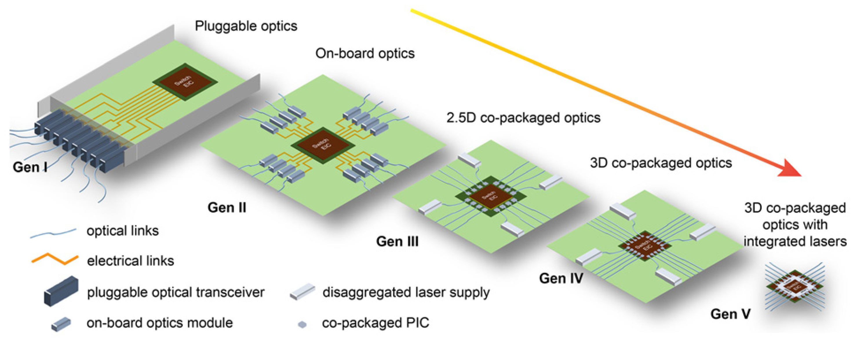
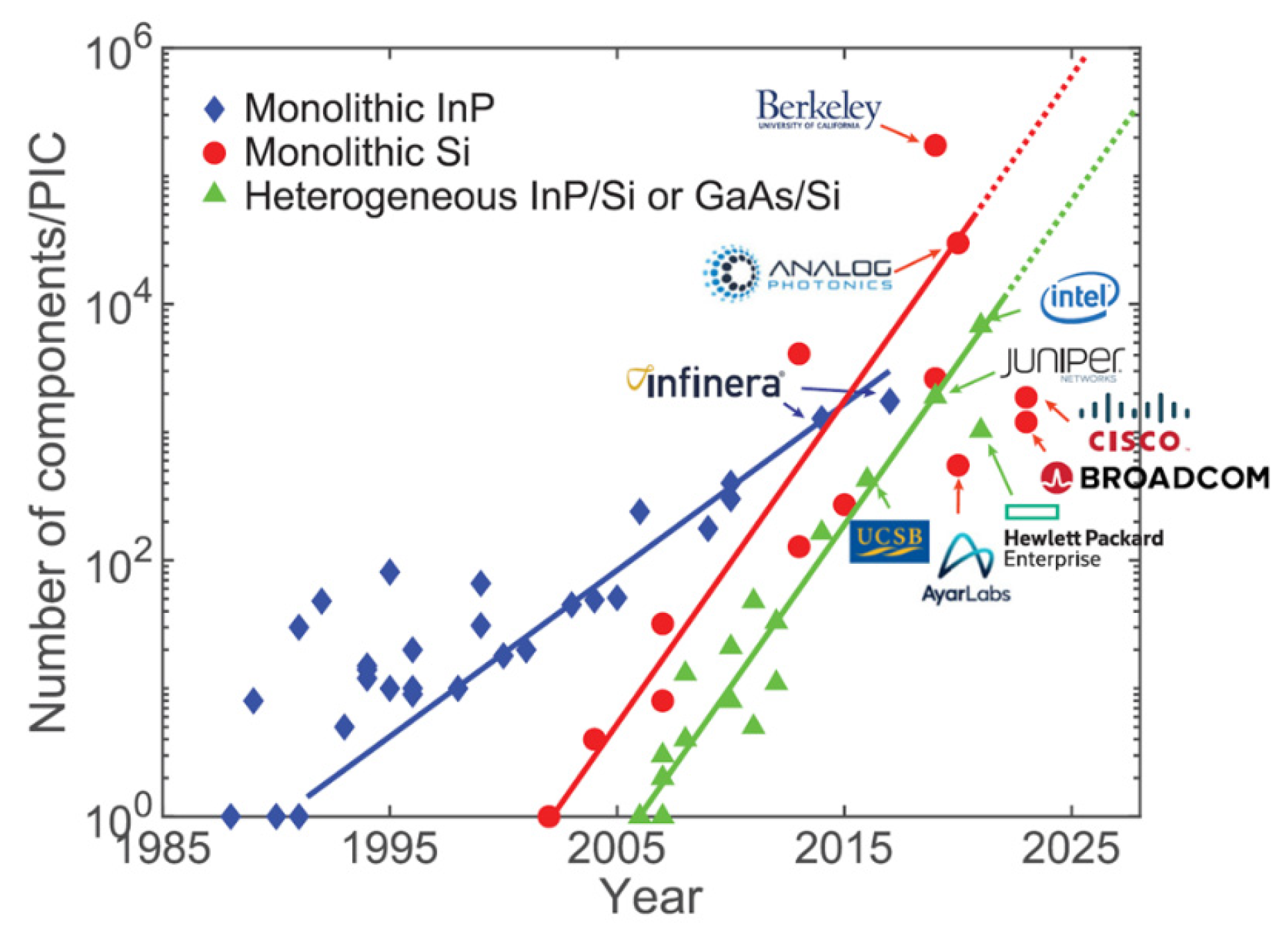
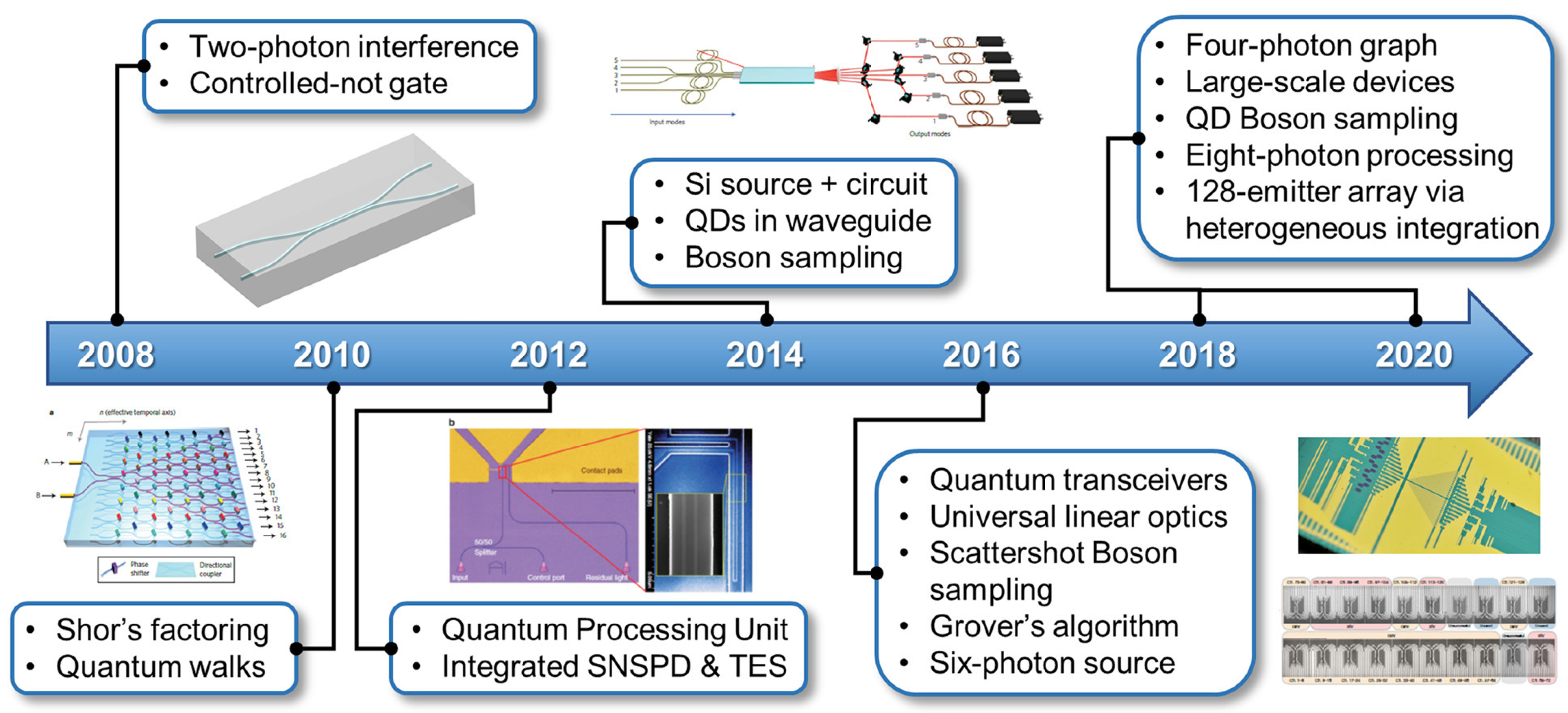
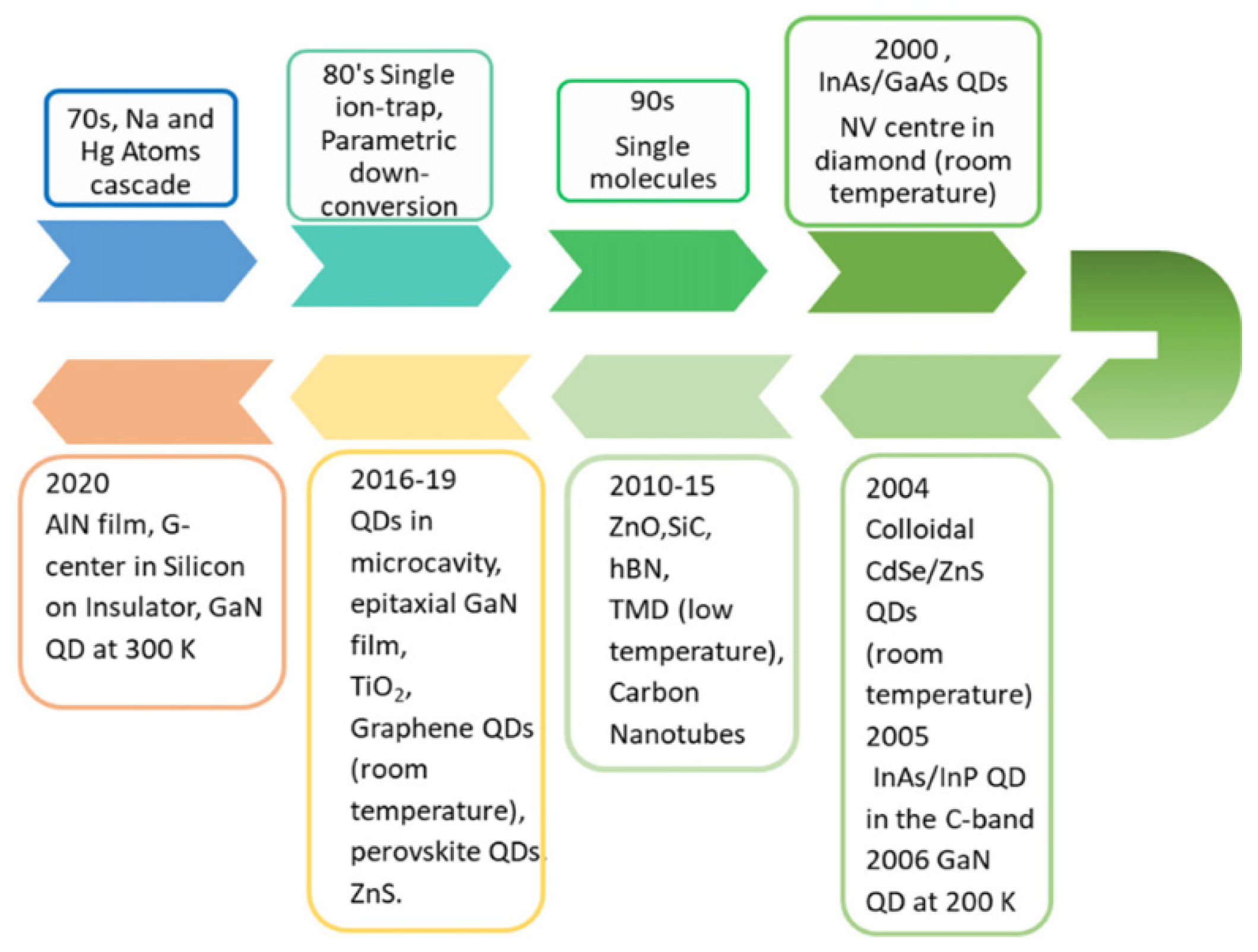
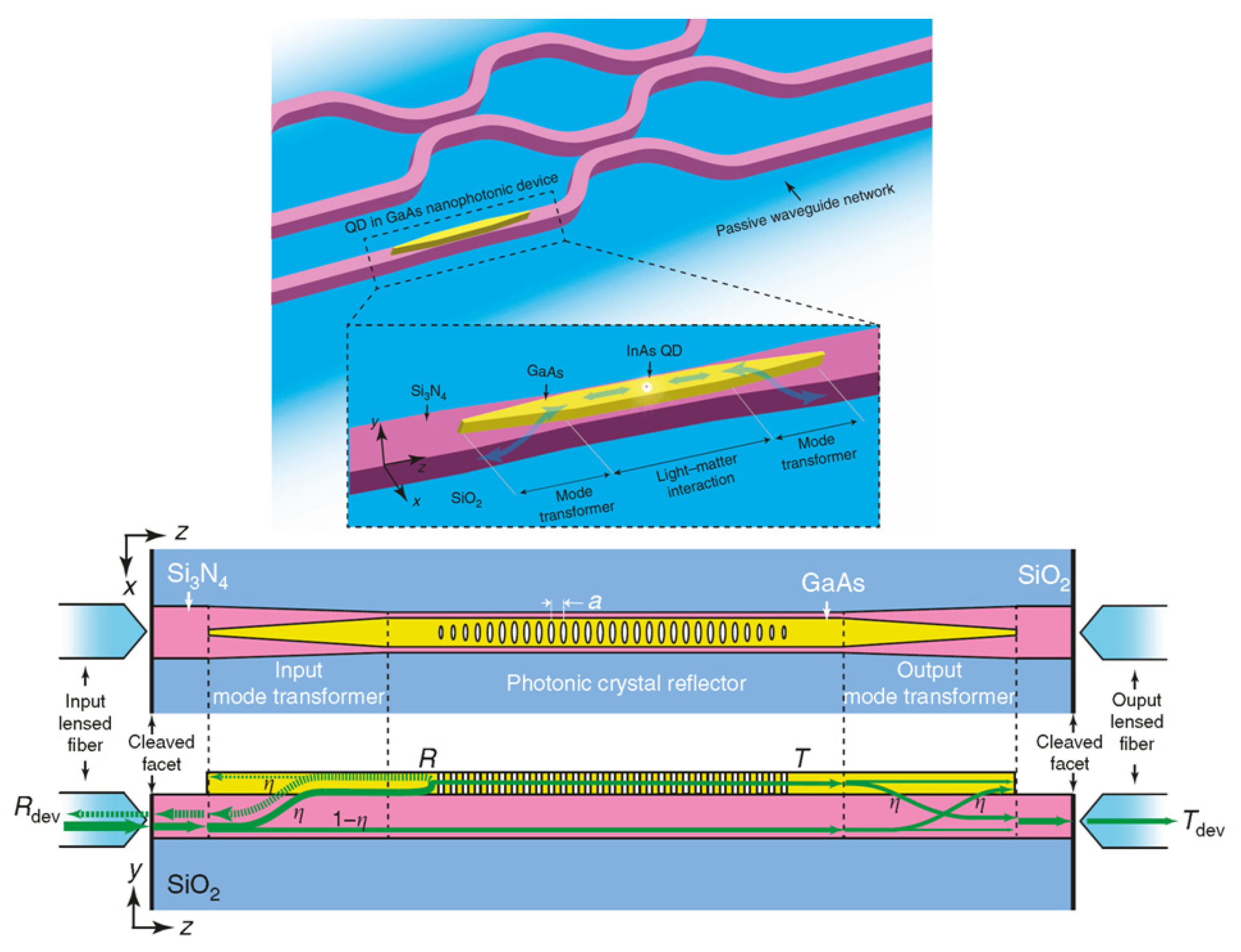
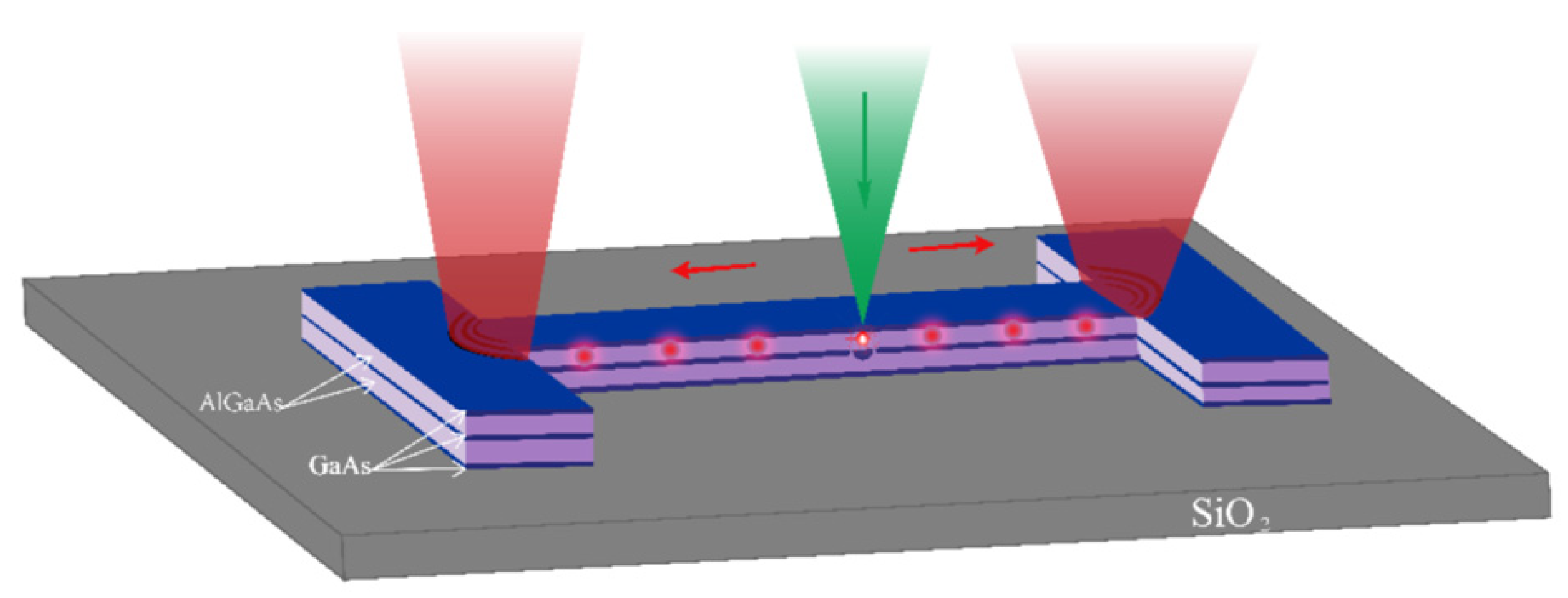
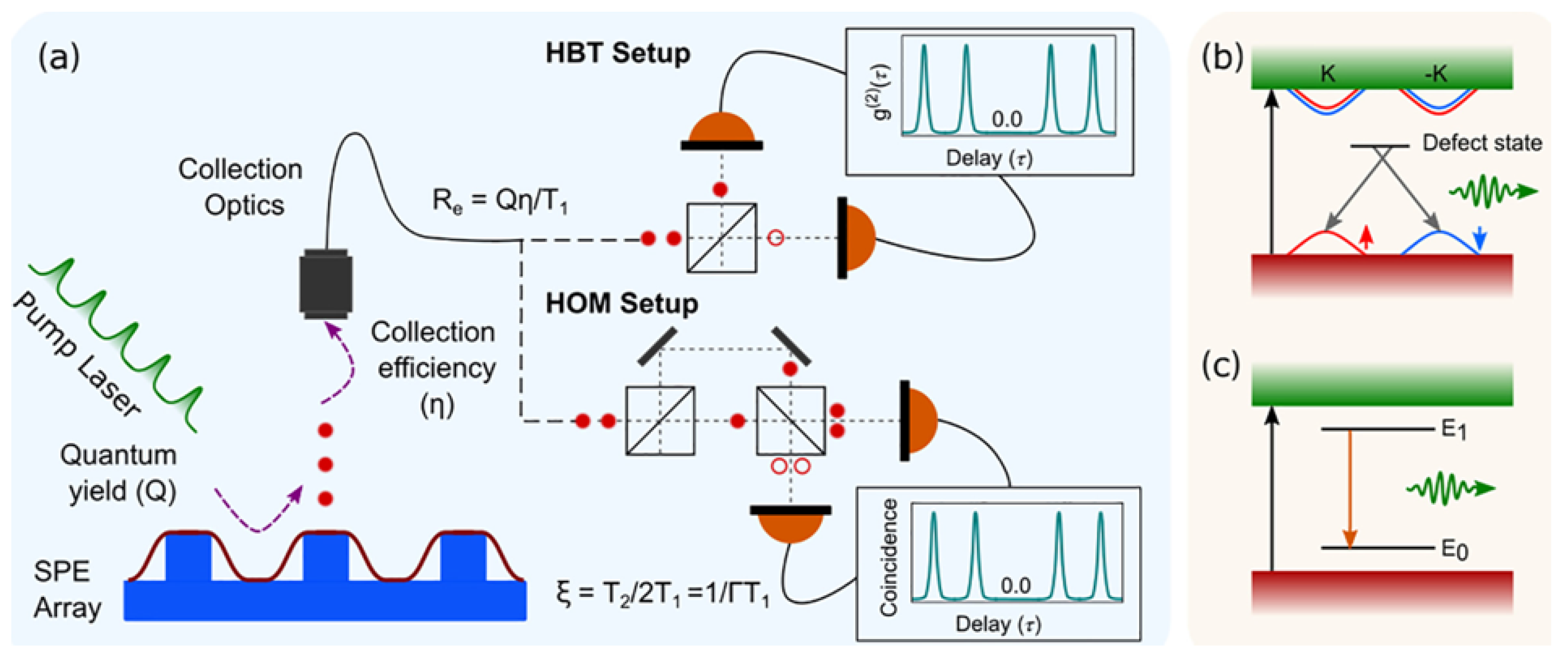
Table 1.
Overview of properties of various epitaxially grown QD single-photon emitters [43].
Table 1.
Overview of properties of various epitaxially grown QD single-photon emitters [43].
| Material System | Wavelength Range | Example g(2)(0) Values | Operating Temperature |
|---|---|---|---|
| InAs/InP | ~1.5 μm | 0.00044 (T = 8 K), 0.006 (T = 4.2 K) | Up to 80 K [g(2)(0) = 0.34] |
| InGaAs/GaAs | ~900 nm–1.55 μm | 0.012–0.03 | Up to 120 K [g(2)(0) = 0.47] |
| GaAs/AlGaAs | ~800–1000 nm | 0.000075 | Up to 80 K [g(2)(0) = 0.28] |
| GaAs/GaAsP | ~750 nm | 0.08 | Up to 160 K [g(2)(0) = 0.48] |
| InP/AlInGaP | ~640–690 nm | 0.05, 0.08, 0.24 | Up to 50 K, Up to 80 K |
| CdSe/ZnSe | ~520–570 nm | 0.07 | Up to 220 K [g(2)(0) = 0.36] |
| CdSe/ZnSSe | ~550 nm | 0.04 (T = 4.5 K), 0.16 (T = 4 K) | Up to 300 K [g(2)(0) = 0.16] |
| CdTe/ZnTe | ~550 nm | 0.14 (T = 6 K) | |
| InGaN/GaN | ~400–600 nm | 0.11 (T = 10 K), 0.13 (T = 5.6 K) | Up to 280 K [g(2)(0) = 0.32] |
| GaN/AlGaN (wz) | ~280–450 nm | 0.02 (T = 10 K) | Up to 350 K [g(2)(0) = 0.34] |
| GaN/AlGaN (zb) | ~330 nm | 0.25 (T = 4 K) | Up to 100 K [g(2)(0) = 0.47] |
Publisher’s Note: MDPI stays neutral with regard to jurisdictional claims in published maps and institutional affiliations. |
© 2021 by the author. Licensee MDPI, Basel, Switzerland. This article is an open access article distributed under the terms and conditions of the Creative Commons Attribution (CC BY) license (https://creativecommons.org/licenses/by/4.0/).
Share and Cite
MDPI and ACS Style
Sasani Ghamsari, M. Chip-Scale Quantum Emitters. Quantum Rep. 2021, 3, 615-642. https://doi.org/10.3390/quantum3040039
AMA Style
Sasani Ghamsari M. Chip-Scale Quantum Emitters. Quantum Reports. 2021; 3(4):615-642. https://doi.org/10.3390/quantum3040039
Chicago/Turabian StyleSasani Ghamsari, Morteza. 2021. "Chip-Scale Quantum Emitters" Quantum Reports 3, no. 4: 615-642. https://doi.org/10.3390/quantum3040039