
Temperature Matters: Enhancing Performance and Stability of Perovskite Solar Cells through Advanced Annealing Methods


Abstract
:1. Introduction
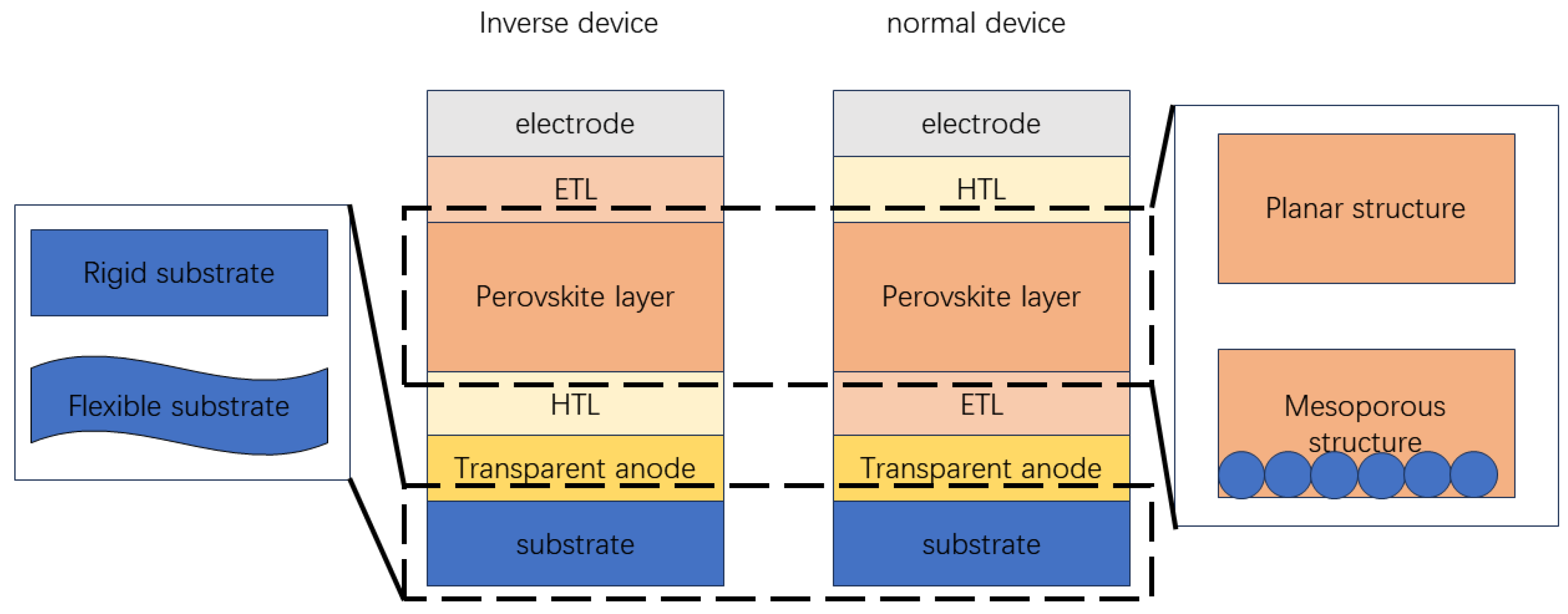
2. Temperature Control in Processing and Preparation
2.1. Electron Transport Layer
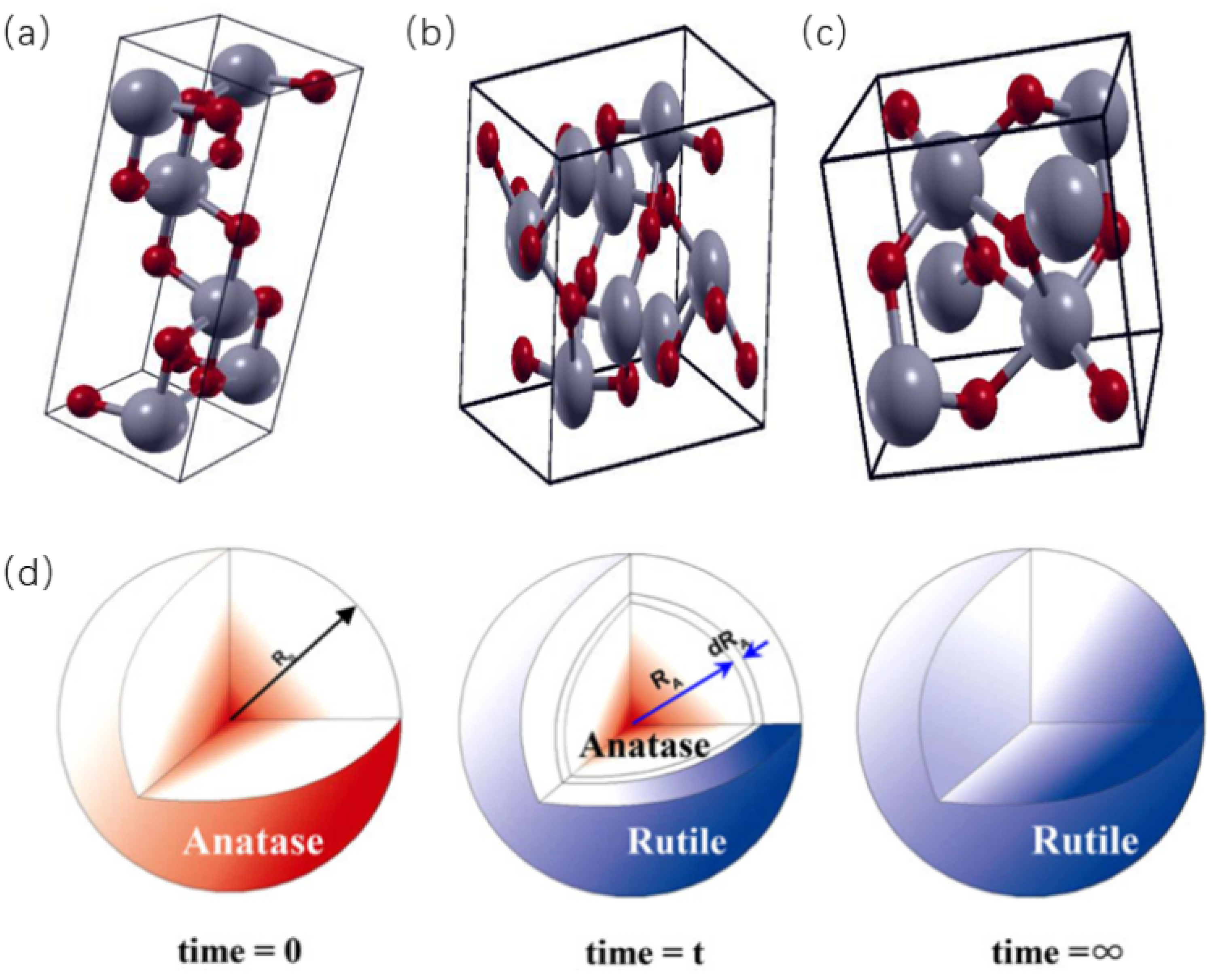
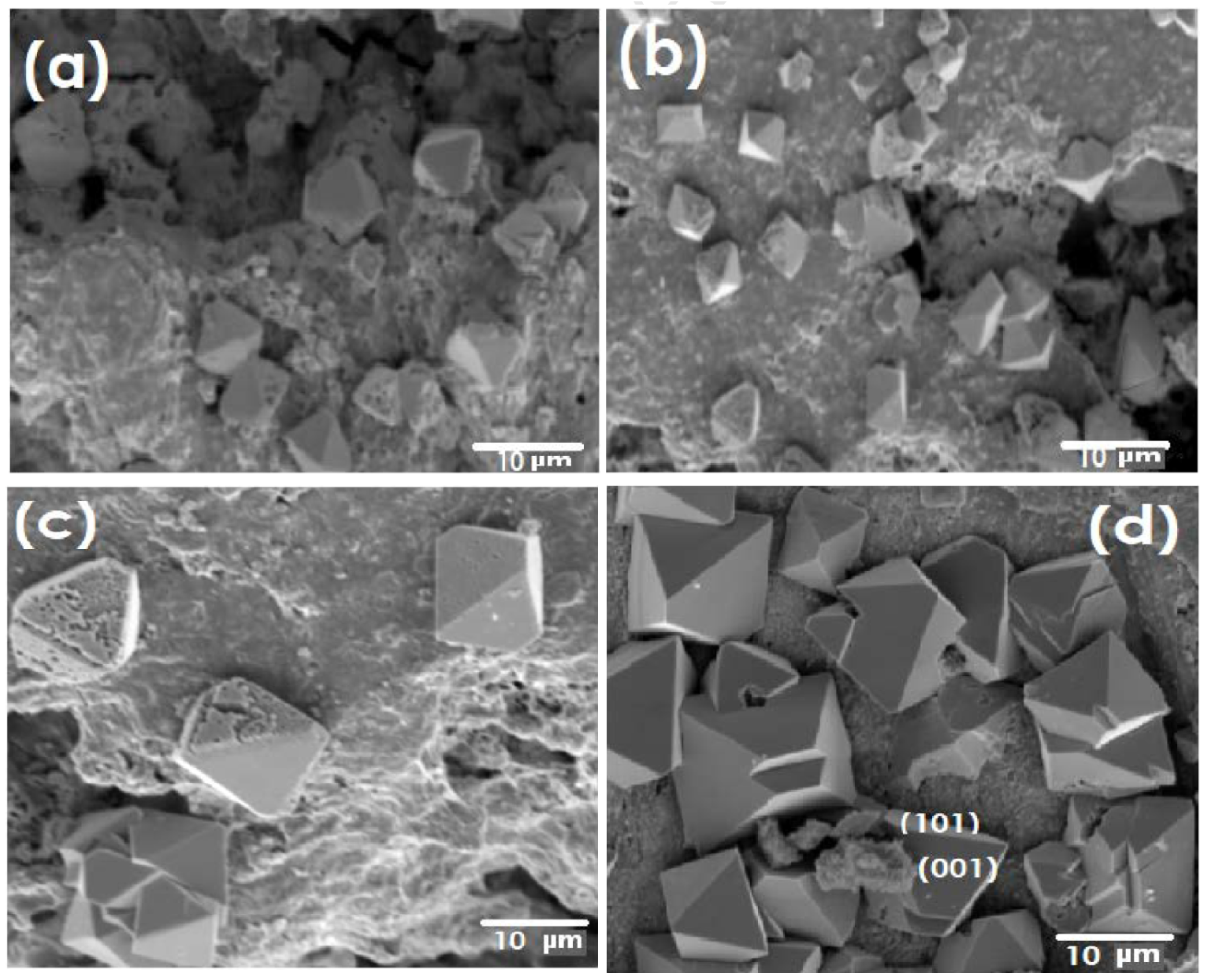
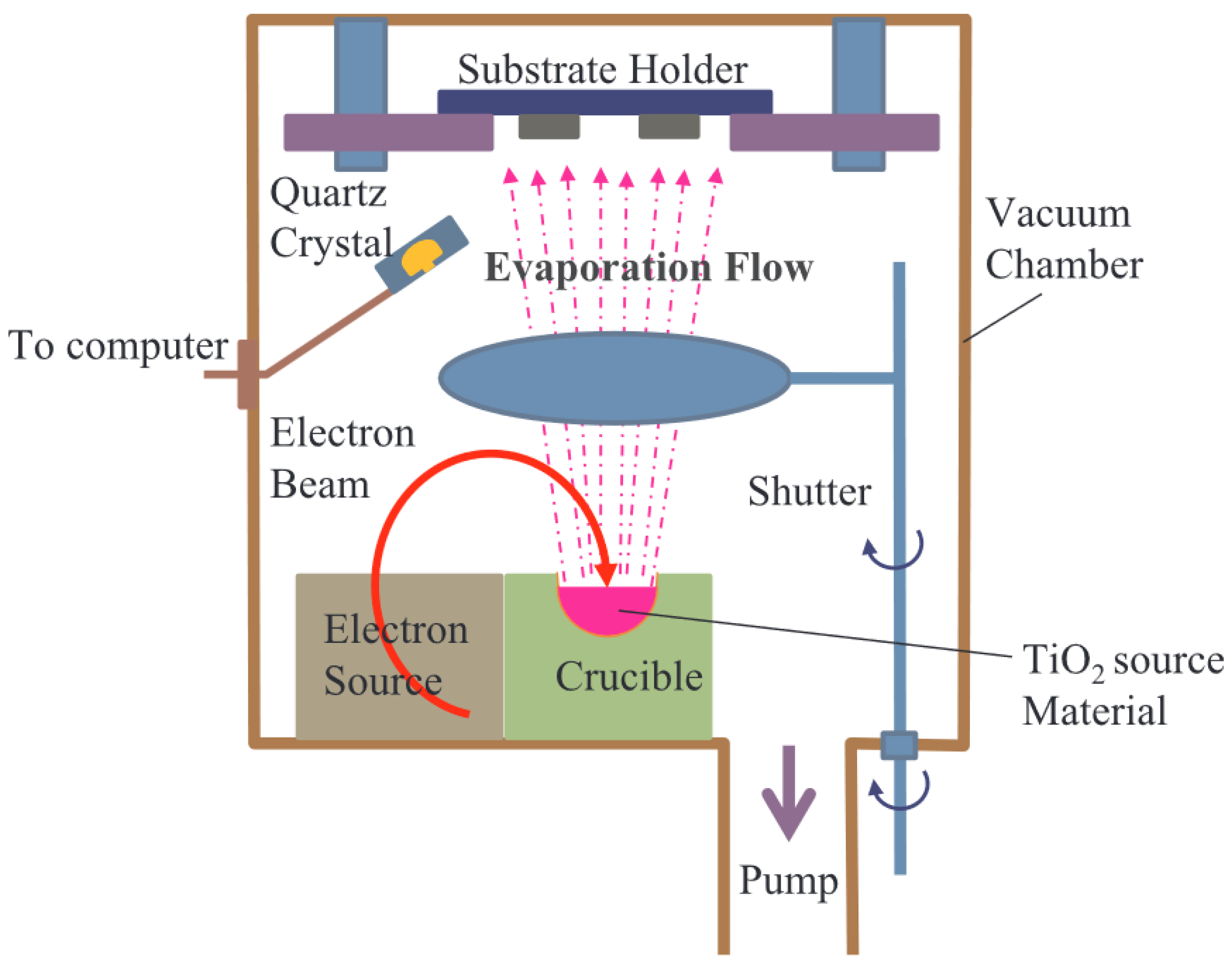
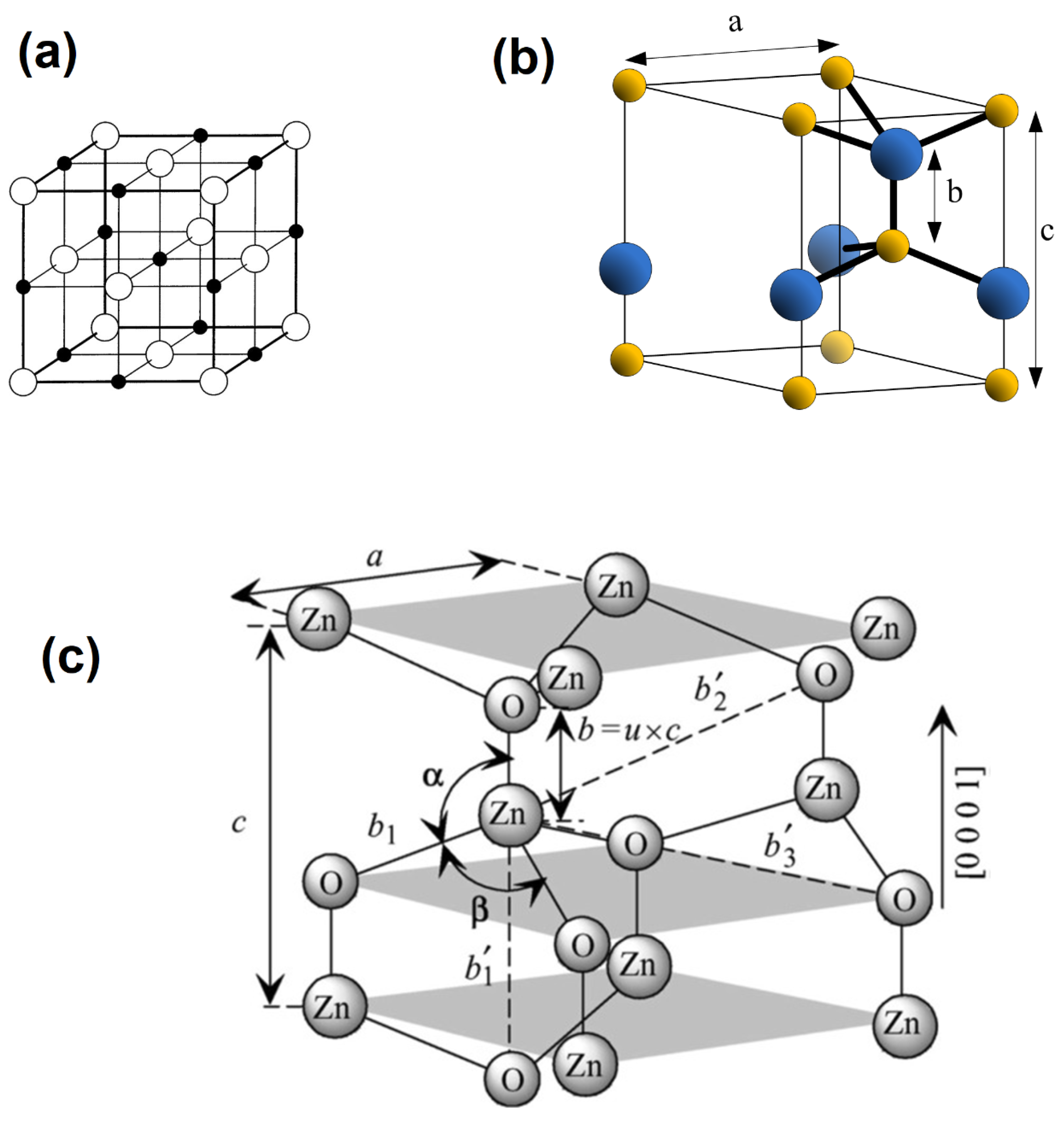
2.1.1. TiO2
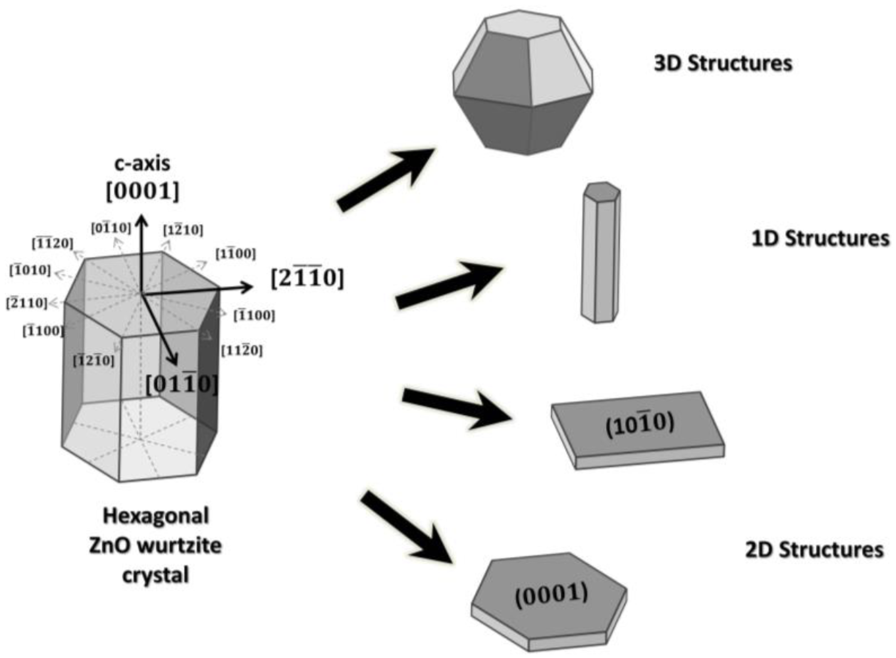
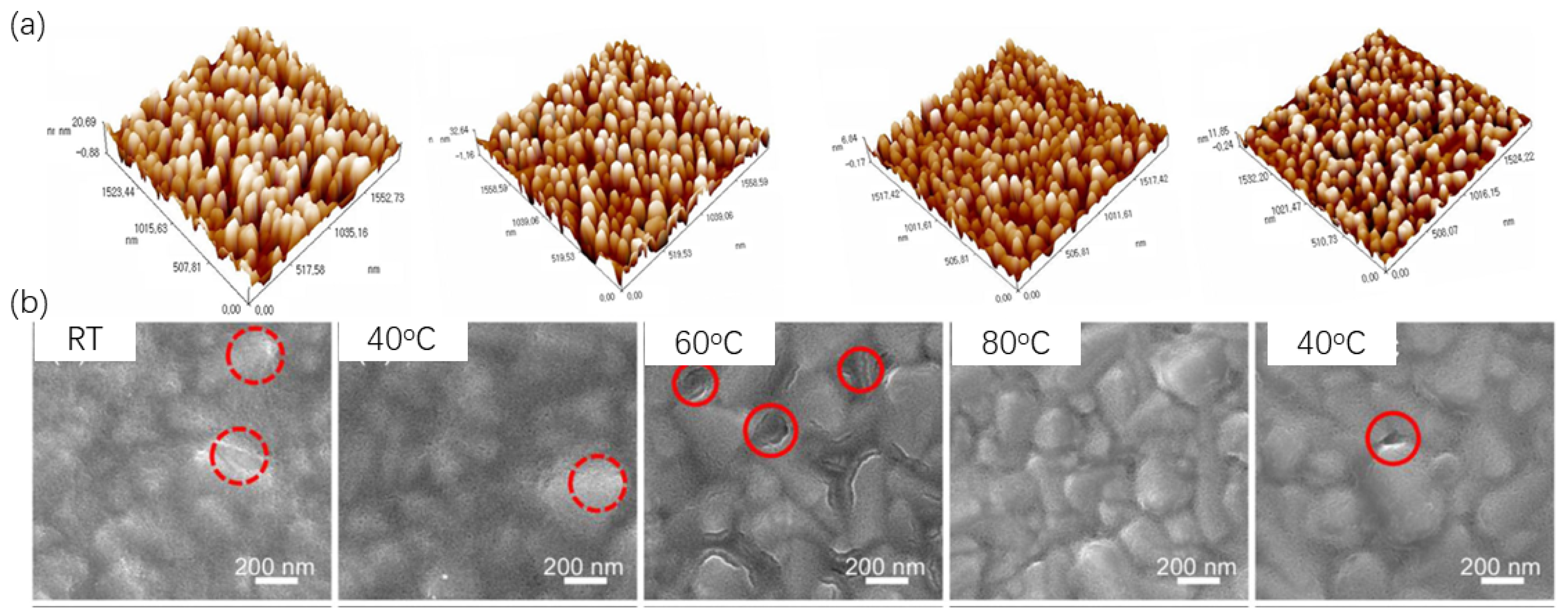
2.1.2. ZnO

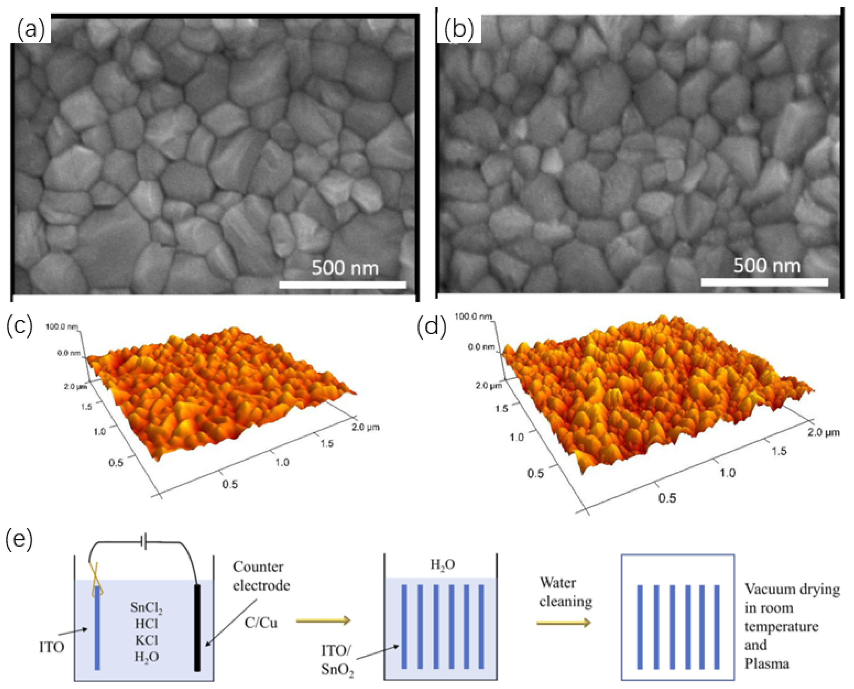
2.1.3. SnO2

2.1.4. PCBM
2.2. Hole Transport Layer
2.2.1. NiOx
2.2.2. Polymer Material
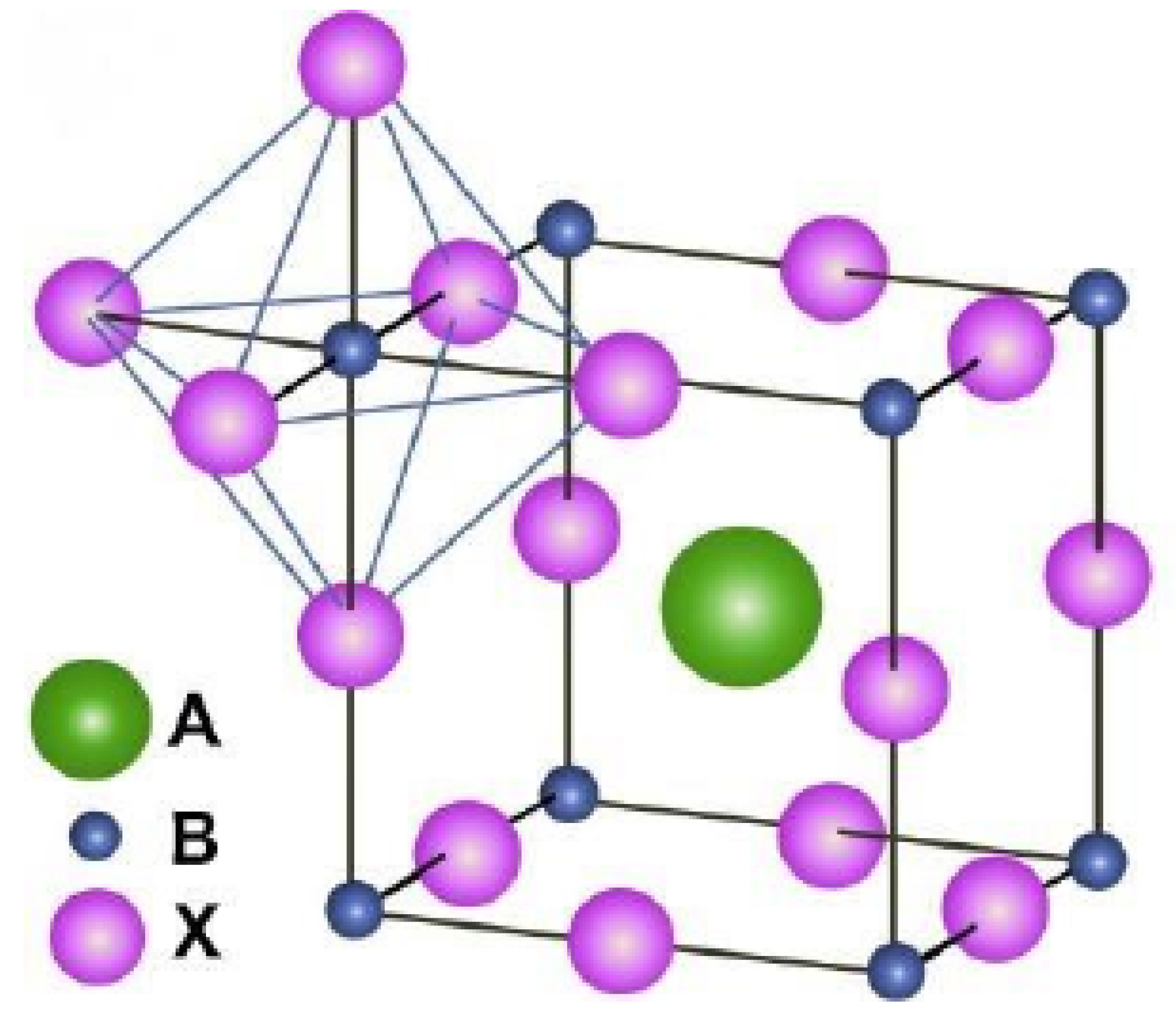
2.3. Perovskite Layer
2.3.1. Effect of Annealing Temperature on Perovskite Material
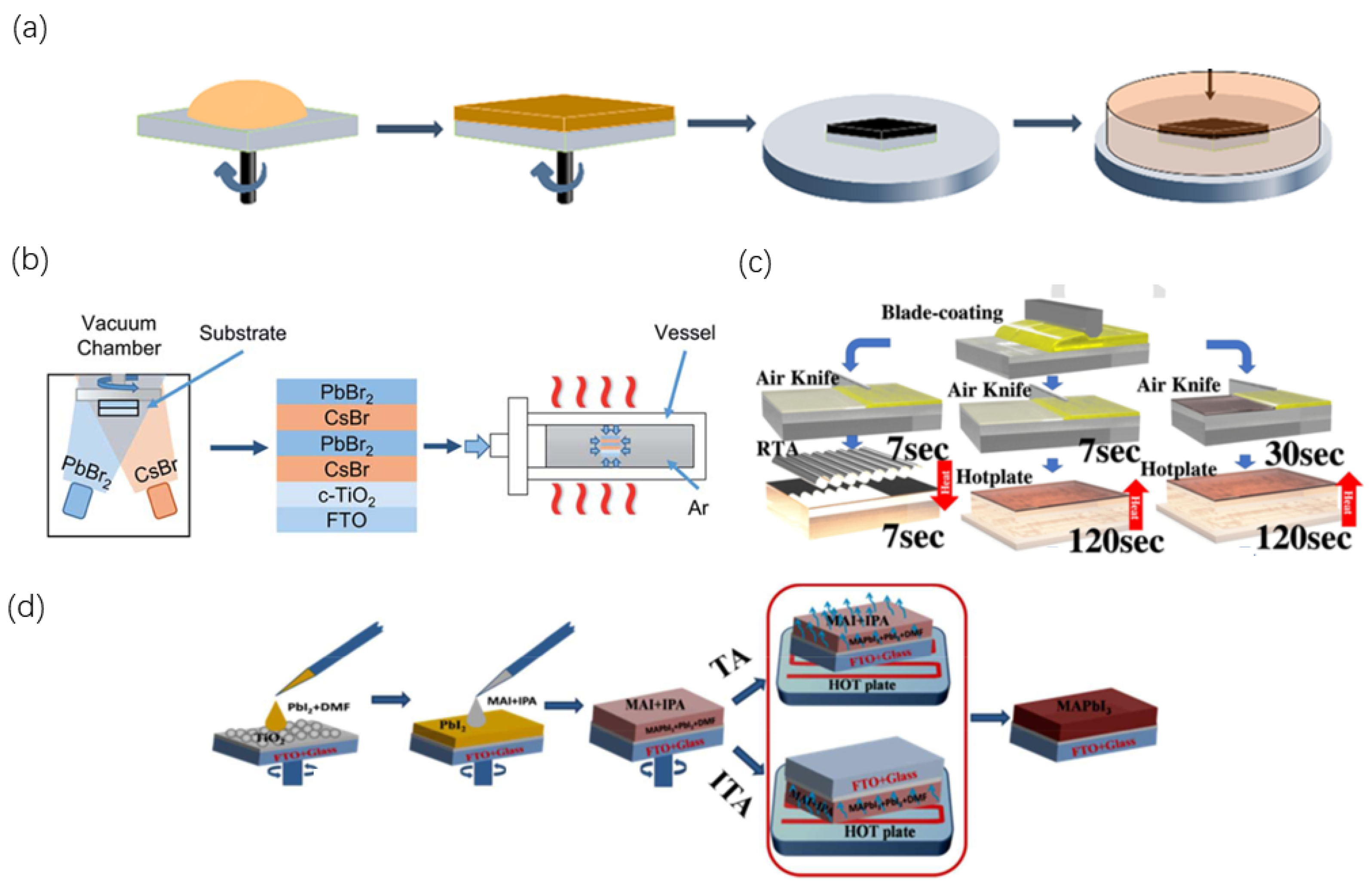
2.3.2. Annealing Methods
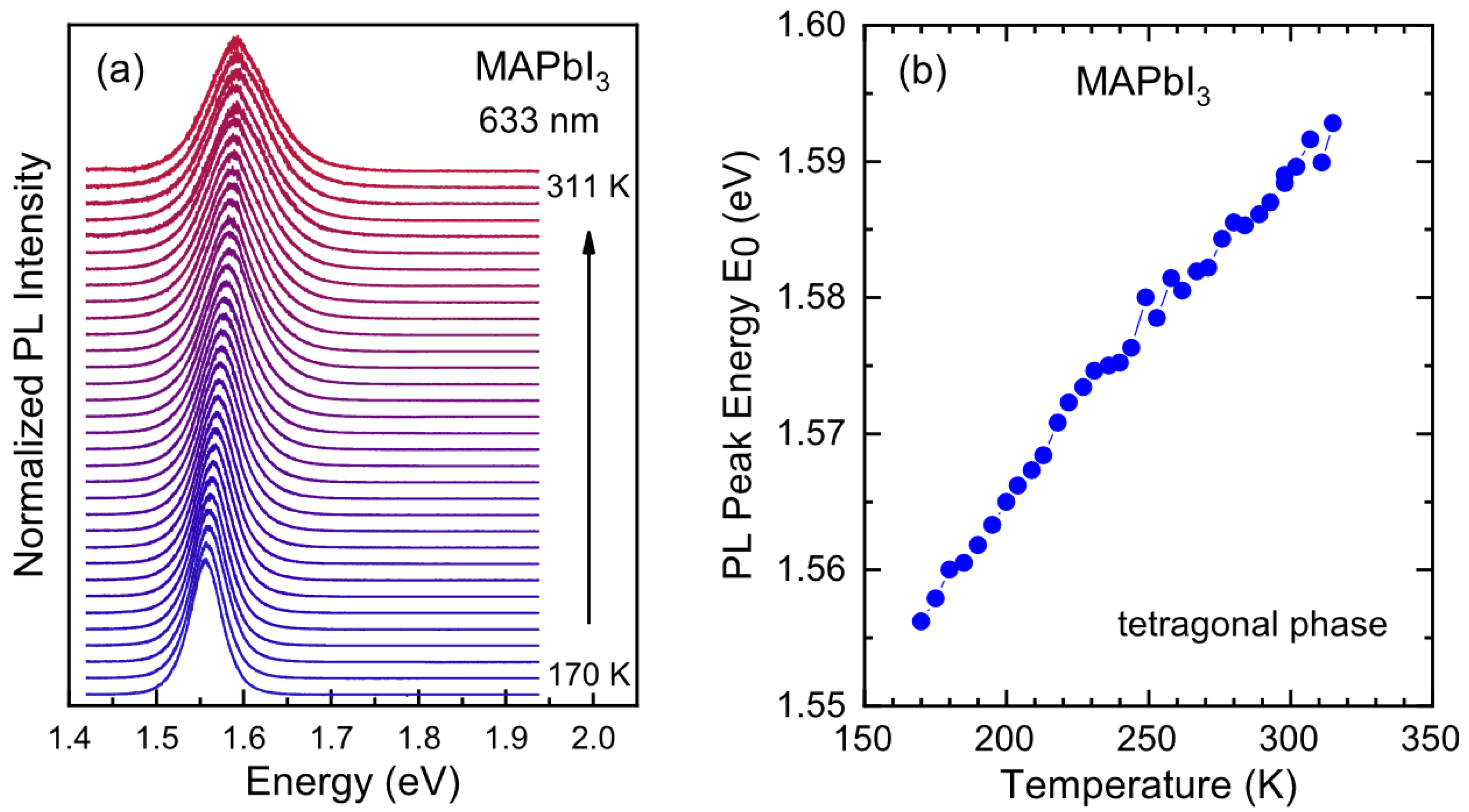
2.3.3. Effect of Temperature on Perovskite under Working Conditions
3. Temperature Coefficient of Perovskite Cells in Operation
4. ISOS Standard and Influence of Operating Temperature
- (1)
- ISOS-D (dark storage studies): The purpose of this test is to provide information on the stability of the solar cell against oxygen, moisture, and other atmospheric components present in the air (such as CO2, NOx, and H2S) and high temperatures. The test is performed in the absence of a light source, without load. Level 1 is room temperature, ambient humidity; Level 2 is 65 or 85 °C with ambient humidity; Level 3 is 65 or 85 °C with 85% relative humidity.
- (2)
- ISOS-V: Electrical bias can cause the degradation of PSCs by controlling the interaction of ions and charges, so electrical bias can also affect the stability of PSCs. Test conditions are as follows: no light source, such as applying positive bias, the bias value can be set to VMPP, Voc, Eg/q, Jsc. If negative bias is applied, the bias value can be set to −Voc, −JMPP. The difference in levels 1, 2, and 3 for this test is the same as ISOS-D. The negative bias is mainly applied to simulate the shadow effect during the operation of the module. Voc represents the partially blocked module with an external bypass diode, and JMPP represents the partially blocked module without an external bypass diode.
- (3)
- ISOS-L (light stability): The light source is recommended to be a sunlight simulator without conditions. It can also be replaced by LED lights or halogen lamps, but to indicate the nature of the light source (will be described in detail in the next part). Level 1 is room temperature, ambient humidity, and load is MPP point voltage or open voltage; Level 2 is 65 or 85 °C, ambient humidity, and the load is MPP point voltage or open voltage; Level 3 is 65 or 85 °C, 50% relative humidity, and the load is MPP point voltage.
- (4)
- ISOS-O (outdoor stability): The light source is sunlight, and the geographical location should be indicated. All levels are outdoor temperature humidity. The difference is that the level 1 load is MPP point voltage or open voltage, the test light source for device performance is sunlight simulator; the Level 2 load is MPP point voltage or open voltage, and the device performance test light source is sunlight; Level 3 load is MPP point voltage, device performance test light source is sunlight simulator and sunlight.
- (5)
- ISOS-T (temperature cycle stability): No light source, no load. Levels 1 and 2 are from room temperature to 65 or 85 °C, ambient humidity; Level 3 is from −40 to 85 °C, with relative humidity of less than 55%.
- (6)
- ISOS-LC (photocycle stability): Since the degradation of PSCs under dark conditions has certain reversibility, the diurnal cycle is simulated by adjusting the light and dark of the light source, the diurnal cycle is simulated by adjusting the light and dark of the light source. Level 1 is room temperature, ambient humidity, and load is MPP point voltage or open voltage; Level 2 is 65 or 85 °C, ambient humidity, and the load is MPP point voltage or open voltage; Level 3 is 65 or 85 °C, less than 50% relative humidity, and the load is MPP point voltage.
- (7)
- ISOS-LT (light temperature cycle stability): The light source is recommended to be a sunlight simulator, which LED lights or halogen lamps can also replace without conditions, and the load is MPP point voltage or open voltage. Level 1 is from room temperature to 65 °C, ambient humidity; Level 2 is from 5 to 65 degrees Celsius, 50% relative humidity; Level 3 is from −25 to 65 °C with 50% relative humidity.
5. Summary and Outlook
- Influence of Temperature on Different Layers:ETL, HTL, and perovskite layer: The temperature during manufacturing significantly affects the surface morphology of the device and has implications for electrical performance and service life. Higher annealing temperatures, for example, can improve film quality, grain size, and overall compactness, enhancing the efficiency of the cells.
- Effect of External Temperature:Limited impact on cell performance: Interestingly, the change in external temperature (presumably during actual operational conditions) has been observed to have little influence on the performance of the cells. This suggests a certain level of robustness or insulation against external temperature variations.
- Need for Improved Annealing Manufacturing Methods:Optimizing annealing processes: Given the significant impact of manufacturing temperature on device characteristics, there is a call to develop more appropriate annealing methods. This optimization is crucial for improving not only the performance but also the stability of photovoltaic devices.
- Broad Application Prospects for PSCs:Positive outlook: Despite the challenges and considerations related to temperature, the overall outlook for perovskite solar cells is optimistic. The expectation is that, with advancements in manufacturing processes and annealing methods, PSCs will have a broad application prospect. This suggests a promising future for perovskite-based photovoltaic technology.
Author Contributions
Funding
Conflicts of Interest
References
- Gao, P.; Grätzel, M.; Nazeeruddin, M.K. Organohalide Lead Perovskites for Photovoltaic Applications. Environ. Sci. 2014, 7, 2448–2463. [Google Scholar] [CrossRef]
- Mohd Yusoff, A.R.B.; Gao, P.; Nazeeruddin, M.K. Recent progress in organohalide lead perovskites for photovoltaic and optoelectronic applications. Coord. Chem. Rev. 2018, 373, 258–294. [Google Scholar] [CrossRef]
- Blancon, J.-C.; Stier, A.V.; Tsai, H.; Nie, W.; Stoumpos, C.C.; Traoré, B.; Pedesseau, L.; Kepenekian, M.; Katsutani, F.; Noe, G.T.; et al. Scaling law for excitons in 2D perovskite quantum wells. Nat. Commun. 2018, 9, 2254. [Google Scholar] [CrossRef] [PubMed]
- Hu, L.; Zhao, Q.; Huang, S.; Zheng, J.; Guan, X.; Patterson, R.; Kim, J.; Shi, L.; Lin, C.-H.; Lei, Q.; et al. Flexible and efficient perovskite quantum dot solar cells via hybrid interfacial architecture. Nat. Commun. 2021, 12, 466. [Google Scholar] [CrossRef] [PubMed]
- Sun, X.; Deng, X.; Li, Z.; Xiong, B.; Zhong, C.; Zhu, Z.; Li, Z.; Jen, A.K. -Y. Dopant-Free Crossconjugated Hole-Transporting Polymers for Highly Efficient Perovskite Solar Cells. Adv. Sci. 2020, 7, 1903331. [Google Scholar] [CrossRef] [PubMed]
- Bella, F.; Griffini, G.; Correa-Baena, J.-P.; Saracco, G.; Grätzel, M.; Hagfeldt, A.; Turri, S.; Gerbaldi, C. Improving efficiency and stability of perovskite solar cells with photocurable fluoropolymers. Science 2016, 354, 203–206. [Google Scholar] [CrossRef]
- Zhang, J.; Sun, Q.; Chen, Q.; Wang, Y.; Zhou, Y.; Song, B.; Yuan, N.; Ding, J.; Li, Y. High Efficiency Planar p-i-n Perovskite Solar Cells Using Low-Cost Fluorene-Based Hole Transporting Material. Adv. Funct. Mater. 2019, 29, 1900484. [Google Scholar] [CrossRef]
- Yu, X.; Zou, X.; Cheng, J.; Chen, D.; Yao, Y.; Chang, C.; Liu, B.; Wang, J.; Zhou, Z.; Li, G. Investigation on Low-temperature Annealing Process of Solution-processed TiO2 Electron Transport Layer for Flexible Perovskite Solar Cell. Materials 2020, 13, 1031. [Google Scholar] [CrossRef] [PubMed]
- Dualeh, A.; Gao, P.; Seok, S.I.; Nazeeruddin, M.K.; Grätzel, M. Thermal Behavior of Methylammonium Lead-Trihalide Perovskite Photovoltaic Light Harvesters. Chem. Mater. 2014, 26, 6160–6164. [Google Scholar] [CrossRef]
- Liu, X.; Wu, J.; Li, G.; Guo, Q.; Song, Z.; Yang, Y.; Wang, X.; Lan, Z.; Lin, J. Defect Control Strategy by Bifunctional Thioacetamide at Low Temperature for Highly Efficient Planar Perovskite Solar Cells. ACS Appl. Mater. Interfaces 2020, 12, 12883–12891. [Google Scholar] [CrossRef] [PubMed]
- Wu, W.-Q.; Chen, D.; Cheng, Y.-B.; Caruso, R.A. Low-Temperature Solution-Processed Amorphous Titania Nanowire Thin Films for 1 cm 2 Perovskite Solar Cells. ACS Appl. Mater. Interfaces 2020, 12, 11450–11458. [Google Scholar] [CrossRef]
- Liu, M.; Johnston, M.B.; Snaith, H.J. Efficient planar heterojunction perovskite solar cells by vapour deposition. Nature 2013, 501, 395–398. [Google Scholar] [CrossRef] [PubMed]
- Tan, H.; Jain, A.; Voznyy, O.; Lan, X.; García De Arquer, F.P.; Fan, J.Z.; Quintero-Bermudez, R.; Yuan, M.; Zhang, B.; Zhao, Y.; et al. Efficient and stable solution-processed planar perovskite solar cells via contact passivation. Science 2017, 355, 722–726. [Google Scholar] [CrossRef] [PubMed]
- Burschka, J.; Pellet, N.; Moon, S.-J.; Humphry-Baker, R.; Gao, P.; Nazeeruddin, M.K.; Grätzel, M. Sequential deposition as a route to high-performance perovskite-sensitized solar cells. Nature 2013, 499, 316–319. [Google Scholar] [CrossRef]
- Lu, H.; Zhong, J.; Ji, C.; Zhao, J.; Li, D.; Zhao, R.; Jiang, Y.; Fang, S.; Liang, T.; Li, H.; et al. Fabricating an optimal rutile TiO2 electron transport layer by delicately tuning TiCl4 precursor solution for high performance perovskite solar cells. Nano Energy 2020, 68, 104336. [Google Scholar] [CrossRef]
- Hu, H.; Dong, B.; Hu, H.; Chen, F.; Kong, M.; Zhang, Q.; Luo, T.; Zhao, L.; Guo, Z.; Li, J.; et al. Atomic Layer Deposition of TiO 2 for a High-Efficiency Hole-Blocking Layer in Hole-Conductor-Free Perovskite Solar Cells Processed in Ambient Air. ACS Appl. Mater. Interfaces 2016, 8, 17999–18007. [Google Scholar] [CrossRef] [PubMed]
- Song, S.; Kang, G.; Pyeon, L.; Lim, C.; Lee, G.-Y.; Park, T.; Choi, J. Systematically Optimized Bilayered Electron Transport Layer for Highly Efficient Planar Perovskite Solar Cells (η = 21.1%). ACS Energy Lett. 2017, 2, 2667–2673. [Google Scholar] [CrossRef]
- Basavaraj, K.; Nyayban, A.; Panda, S. Structural phase transitions and elastic properties of TiO 2 polymorphs: Ab-initio study. IOP Conf. Ser. Mater. Sci. Eng. 2022, 1248, 012064. [Google Scholar] [CrossRef]
- Reyes-Coronado, D.; Rodríguez-Gattorno, G.; Espinosa-Pesqueira, M.E.; Cab, C.; De Coss, R.; Oskam, G. Phase-pure TiO2 nanoparticles: Anatase, brookite and rutile. Nanotechnology 2008, 19, 145605. [Google Scholar] [CrossRef] [PubMed]
- Shannon, R.D.; Pask, J.A. Kinetics of the Anatase-Rutile Transformation. J. Am. Ceram. Soc. 1965, 48, 391–398. [Google Scholar] [CrossRef]
- Varghese, O.K.; Gong, D.; Paulose, M.; Grimes, C.A.; Dickey, E.C. Crystallization and high-temperature structural stability of titanium oxide nanotube arrays. J. Mater. Res. 2003, 18, 156–165. [Google Scholar] [CrossRef]
- Rambabu, Y.; Jaiswal, M.; Roy, S.C. Effect of annealing temperature on the phase transition, structural stability and photo-electrochemical performance of TiO2 multi-leg nanotubes. Catal. Today 2016, 278, 255–261. [Google Scholar] [CrossRef]
- Ma, J.-S.; Wen, M.-C.; Lu, C.-H. Reaction mechanism and kinetics analysis of the phase transformation of TiO2 from the anatase phase to the rutile phase. J. Mater. Sci. Mater. Electron. 2013, 24, 2506–2512. [Google Scholar] [CrossRef]
- Lin, L.; Jones, T.W.; Yang, T.C.; Duffy, N.W.; Li, J.; Zhao, L.; Chi, B.; Wang, X.; Wilson, G.J. Inorganic Electron Transport Materials in Perovskite Solar Cells. Adv. Funct. Mater. 2021, 31, 2008300. [Google Scholar] [CrossRef]
- Hu, X.; Liu, C.; Zhang, Z.; Jiang, X.; Garcia, J.; Sheehan, C.; Shui, L.; Priya, S.; Zhou, G.; Zhang, S.; et al. 22% Efficiency Inverted Perovskite Photovoltaic Cell Using Cation-Doped Brookite TiO2 Top Buffer. Adv. Sci. 2020, 7, 2001285. [Google Scholar] [CrossRef] [PubMed]
- Kogo, A.; Sanehira, Y.; Ikegami, M.; Miyasaka, T. Brookite TiO2 as a low-temperature solution-processed mesoporous layer for hybrid perovskite solar cells. J. Mater. Chem. A 2015, 3, 20952–20957. [Google Scholar] [CrossRef]
- Wang, Y.; Wan, J.; Ding, J.; Hu, J.; Wang, D. A Rutile TiO 2 Electron Transport Layer for the Enhancement of Charge Collection for Efficient Perovskite Solar Cells. Angew. Chem. Int. Ed. 2019, 58, 9414–9418. [Google Scholar] [CrossRef] [PubMed]
- Shahvaranfard, F.; Altomare, M.; Hou, Y.; Hejazi, S.; Meng, W.; Osuagwu, B.; Li, N.; Brabec, C.J.; Schmuki, P. Engineering of the Electron Transport Layer/Perovskite Interface in Solar Cells Designed on TiO2 Rutile Nanorods. Adv. Funct. Mater. 2020, 30, 1909738. [Google Scholar] [CrossRef]
- Malevu, T.D.; Mwankemwa, B.S.; Motloung, S.V.; Tshabalala, K.G.; Ocaya, R.O. Effect of annealing temperature on nano-crystalline TiO2 for solar cell applications. Phys. E Low-Dimens. Syst. Nanostruct. 2019, 106, 127–132. [Google Scholar] [CrossRef]
- Hossain, M.F. Annealing effect of E-beam evaporated TiO2 films and their performance in perovskite solar cells. J. Photochem. 2018, 360, 109–116. [Google Scholar] [CrossRef]
- Lv, Y.; Yuan, R.; Cai, B.; Bahrami, B.; Chowdhury, A.H.; Yang, C.; Wu, Y.; Qiao, Q.; Liu, S.; Zhang, W. High-Efficiency Perovskite Solar Cells Enabled by Anatase TiO 2 Nanopyramid Arrays with an Oriented Electric Field. Angew. Chem. 2020, 132, 12067–12074. [Google Scholar] [CrossRef]
- Kim, B.J.; Kim, D.H.; Lee, Y.-Y.; Shin, H.-W.; Han, G.S.; Hong, J.S.; Mahmood, K.; Ahn, T.K.; Joo, Y.-C.; Hong, K.S.; et al. Highly efficient and bending durable perovskite solar cells: Toward a wearable power source. Energy Environ. Sci. 2015, 8, 916–921. [Google Scholar] [CrossRef]
- Hsu, C.-H.; Chen, K.-T.; Lin, L.-Y.; Wu, W.-Y.; Liang, L.-S.; Gao, P.; Qiu, Y.; Zhang, X.-Y.; Huang, P.-H.; Lien, S.-Y.; et al. Tantalum-Doped TiO2 Prepared by Atomic Layer Deposition and Its Application in Perovskite Solar Cells. Nanomaterials 2021, 11, 1504. [Google Scholar] [CrossRef] [PubMed]
- Manabeng, M.; Mwankemwa, B.S.; Ocaya, R.O.; Motaung, T.E.; Malevu, T.D. A Review of the Impact of Zinc Oxide Nanostructure Morphology on Perovskite Solar Cell Performance. Processes 2022, 10, 1803. [Google Scholar] [CrossRef]
- Fakharuddin, A.; Di Giacomo, F.; Ahmed, I.; Wali, Q.; Brown, T.M.; Jose, R. Role of morphology and crystallinity of nanorod and planar electron transport layers on the performance and long term durability of perovskite solar cells. J. Power Sources 2015, 283, 61–67. [Google Scholar] [CrossRef]
- Tang, J.-F.; Tseng, Z.-L.; Chen, L.-C.; Chu, S.-Y. ZnO nanowalls grown at low-temperature for electron collection in high-efficiency perovskite solar cells. Sol. Energy Mater. Sol. Cells 2016, 154, 18–22. [Google Scholar] [CrossRef]
- Leonardi, S. Two-Dimensional Zinc Oxide Nanostructures for Gas Sensor Applications. Chemosensors 2017, 5, 17. [Google Scholar] [CrossRef]
- Li, Y.-F. First-Principles Prediction of the ZnO Morphology in the Perovskite Solar Cell. J. Phys. Chem. C 2019, 123, 14164–14172. [Google Scholar] [CrossRef]
- Cao, H.L.; Qian, X.F.; Gong, Q.; Du, W.M.; Ma, X.D.; Zhu, Z.K. Shape- and size-controlled synthesis of nanometre ZnO from a simple solution route at room temperature. Nanotechnology 2006, 17, 3632–3636. [Google Scholar] [CrossRef]
- Pan, Z.W.; Dai, Z.R.; Wang, Z.L. Nanobelts of Semiconducting Oxides. Science 2001, 291, 1947–1949. [Google Scholar] [CrossRef]
- Adnan, M.; Usman, M.; Ali, S.; Javed, S.; Islam, M.; Akram, M.A. Aluminum Doping Effects on Interface Depletion Width of Low Temperature Processed ZnO Electron Transport Layer-Based Perovskite Solar Cells. Front. Chem. 2022, 9, 795291. [Google Scholar] [CrossRef]
- Niu, H.; Fang, C.; Wei, X.; Wang, H.; Wan, L.; Li, Y.; Mao, X.; Xu, J.; Zhou, R. Magnetron sputtered ZnO electron transporting layers for high performance perovskite solar cells. Dalton Trans. 2021, 50, 6477–6487. [Google Scholar] [CrossRef] [PubMed]
- Yun, S.; Guo, T.; Li, Y.; Gao, X.; Huang, A.; Kang, L. Well-ordered vertically aligned ZnO nanorods arrays for high-performance perovskite solar cells. Mater. Res. Bull. 2020, 130, 110935. [Google Scholar] [CrossRef]
- Al Jarrah, R.M.; Kadhem, E.M.; Alkhayatt, A.H.O. Annealing and operating temperatures effect on spray-deposited nanocrystalline ZnO thin-film gas sensor. Appl. Phys. A 2022, 128, 527. [Google Scholar] [CrossRef]
- Khambunkoed, N.; Homnan, S.; Gardchareon, A.; Chattrapiban, N.; Songsiriritthigul, P.; Wongratanaphisan, D.; Ruankham, P. Fully-covered slot-die-coated ZnO thin films for reproducible carbon-based perovskite solar cells. Mater. Sci. Semicond. Process. 2021, 136, 106151. [Google Scholar] [CrossRef]
- Zhou, Y.; Li, X.; Lin, H. To Be Higher and Stronger—Metal Oxide Electron Transport Materials for Perovskite Solar Cells. Small 2020, 16, 1902579. [Google Scholar] [CrossRef] [PubMed]
- Dong, Q.; Shi, Y.; Wang, K.; Li, Y.; Wang, S.; Zhang, H.; Xing, Y.; Du, Y.; Bai, X.; Ma, T. Insight into Perovskite Solar Cells Based on SnO 2 Compact Electron-Selective Layer. J. Phys. Chem. C 2015, 119, 10212–10217. [Google Scholar] [CrossRef]
- Xiong, L.; Guo, Y.; Wen, J.; Liu, H.; Yang, G.; Qin, P.; Fang, G. Review on the Application of SnO2 in Perovskite Solar Cells. Adv. Funct. Mater. 2018, 28, 1802757. [Google Scholar] [CrossRef]
- Ke, W.; Zhao, D.; Cimaroli, A.J.; Grice, C.R.; Qin, P.; Liu, Q.; Xiong, L.; Yan, Y.; Fang, G. Effects of annealing temperature of tin oxide electron selective layers on the performance of perovskite solar cells. J. Mater. Chem. A 2015, 3, 24163–24168. [Google Scholar] [CrossRef]
- Wang, Y.; Gao, P.; Fan, X.; Li, J.; Guo, P.; Huang, L.; Sun, J. Effect of SnO2 Annealing Temperature on the Performance of Perovskite Solar Cells. J. Inorg. Mater. 2021, 36, 168. [Google Scholar] [CrossRef]
- Progress and Challenges of SnO2 Electron Transport Layer for Perovskite Solar Cells: A Critical Review. Available online: https://onlinelibrary.wiley.com/doi/epdf/10.1002/solr.202100983 (accessed on 24 July 2023).
- Wang, Q.; Peng, C.; Du, L.; Li, H.; Zhang, W.; Xie, J.; Qi, H.; Li, Y.; Tian, L.; Huang, Y. Enhanced Performance of Perovskite Solar Cells via Low-Temperature-Processed Mesoporous SnO2. Adv. Mater. Int. 2020, 7, 1901866. [Google Scholar] [CrossRef]
- Jia, J.; Dong, J.; Wu, J.; Wei, H.; Cao, B. Combustion procedure deposited SnO2 electron transport layers for high efficient perovskite solar cells. J. Alloys Compd. 2020, 844, 156032. [Google Scholar] [CrossRef]
- Liu, J.; Li, N.; Dong, Q.; Li, J.; Qin, C.; Wang, L. Tailoring electrical property of the low-temperature processed SnO2 for high-performance perovskite solar cells. Sci. China Mater. 2019, 62, 173–180. [Google Scholar] [CrossRef]
- Sun, Y.; Zhang, J.; Yu, H. Room-temperature electrochemically deposited polycrystalline SnO2 with adjustable work function for high-efficiency perovskite solar cells. J. Mater. Chem. A 2023, 11, 901–913. [Google Scholar] [CrossRef]
- Xu, J.; Buin, A.; Ip, A.H.; Li, W.; Voznyy, O.; Comin, R.; Yuan, M.; Jeon, S.; Ning, Z.; McDowell, J.J.; et al. Perovskite–fullerene hybrid materials suppress hysteresis in planar diodes. Nat. Commun. 2015, 6, 7081. [Google Scholar] [CrossRef] [PubMed]
- Jeng, J.; Chiang, Y.; Lee, M.; Peng, S.; Guo, T.; Chen, P.; Wen, T. CH3 NH3 PbI3 Perovskite/Fullerene Planar-Heterojunction Hybrid Solar Cells. Adv. Mater. 2013, 25, 3727–3732. [Google Scholar] [CrossRef]
- Sun, S.; Salim, T.; Mathews, N.; Duchamp, M.; Boothroyd, C.; Xing, G.; Sum, T.C.; Lam, Y.M. The origin of high efficiency in low-temperature solution-processable bilayer organometal halide hybrid solar cells. Energy Environ. Sci. 2014, 7, 399–407. [Google Scholar] [CrossRef]
- Niu, G.; Wang, S.; Li, J.; Li, W.; Wang, L. Oxygen doping in nickel oxide for highly efficient planar perovskite solar cells. J. Mater. Chem. A 2018, 6, 4721–4728. [Google Scholar] [CrossRef]
- Shao, Y.; Xiao, Z.; Bi, C.; Yuan, Y.; Huang, J. Origin and elimination of photocurrent hysteresis by fullerene passivation in CH3NH3PbI3 planar heterojunction solar cells. Nat. Commun. 2014, 5, 5784. [Google Scholar] [CrossRef]
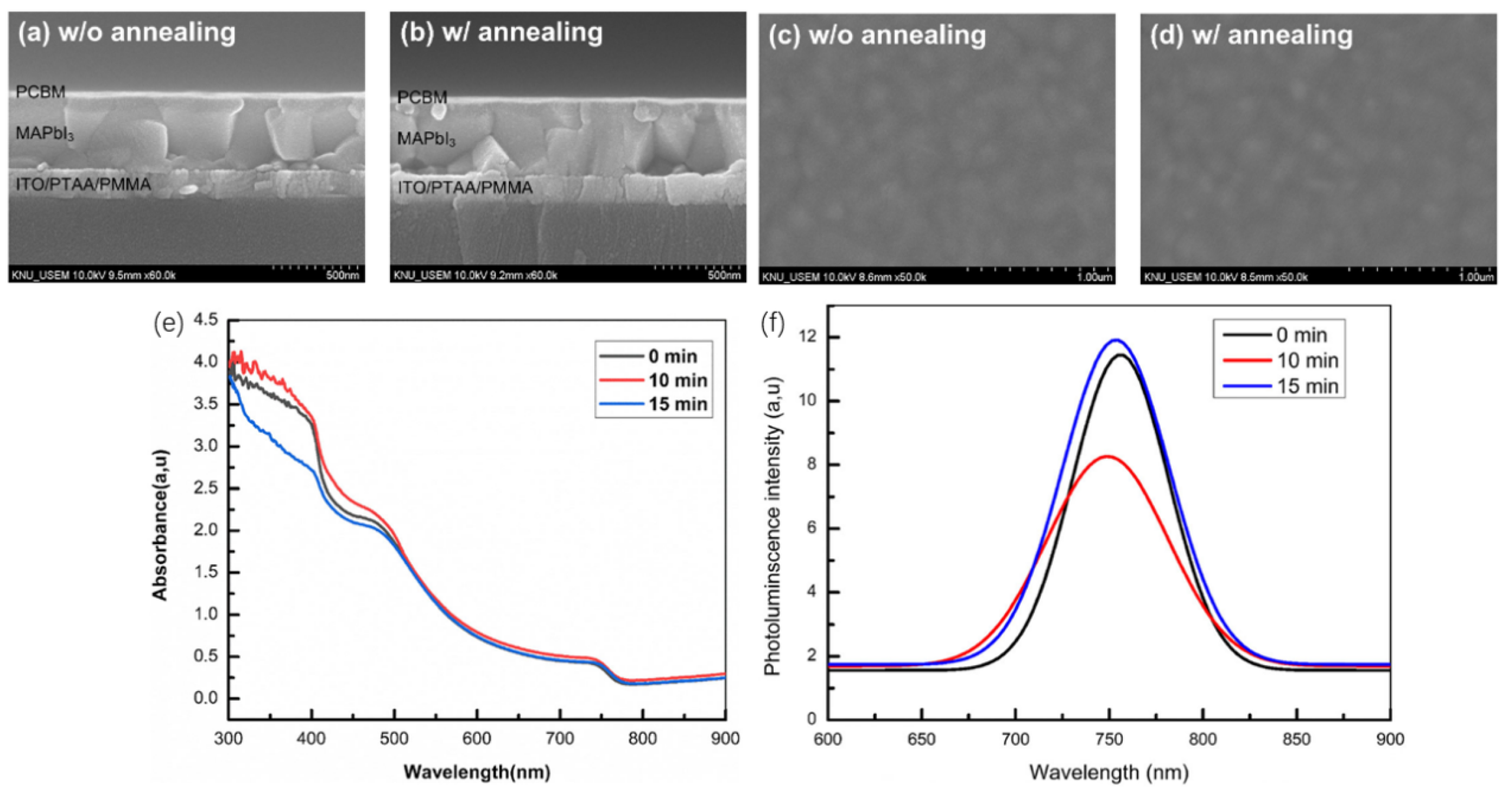
- Choi, S.; Shin, W.; Oh, J.; Ryu, M.-Y.; Lee, H. Enhancement in Device Performance of Perovskite Solar Cells via Annealing of PCBM Electron Transport Layer. Appl. Sci. Converg. Technol. 2022, 31, 167–170. [Google Scholar] [CrossRef]
- Mehdi, H.; Selmi, O.; Mhamdi, A.; Bouazizi, A. Effect of annealing treatment of PC60BM layer on inverted perovskite solar cells. J. Mater. Sci. Mater. Electron. 2022, 33, 5351–5358. [Google Scholar] [CrossRef]
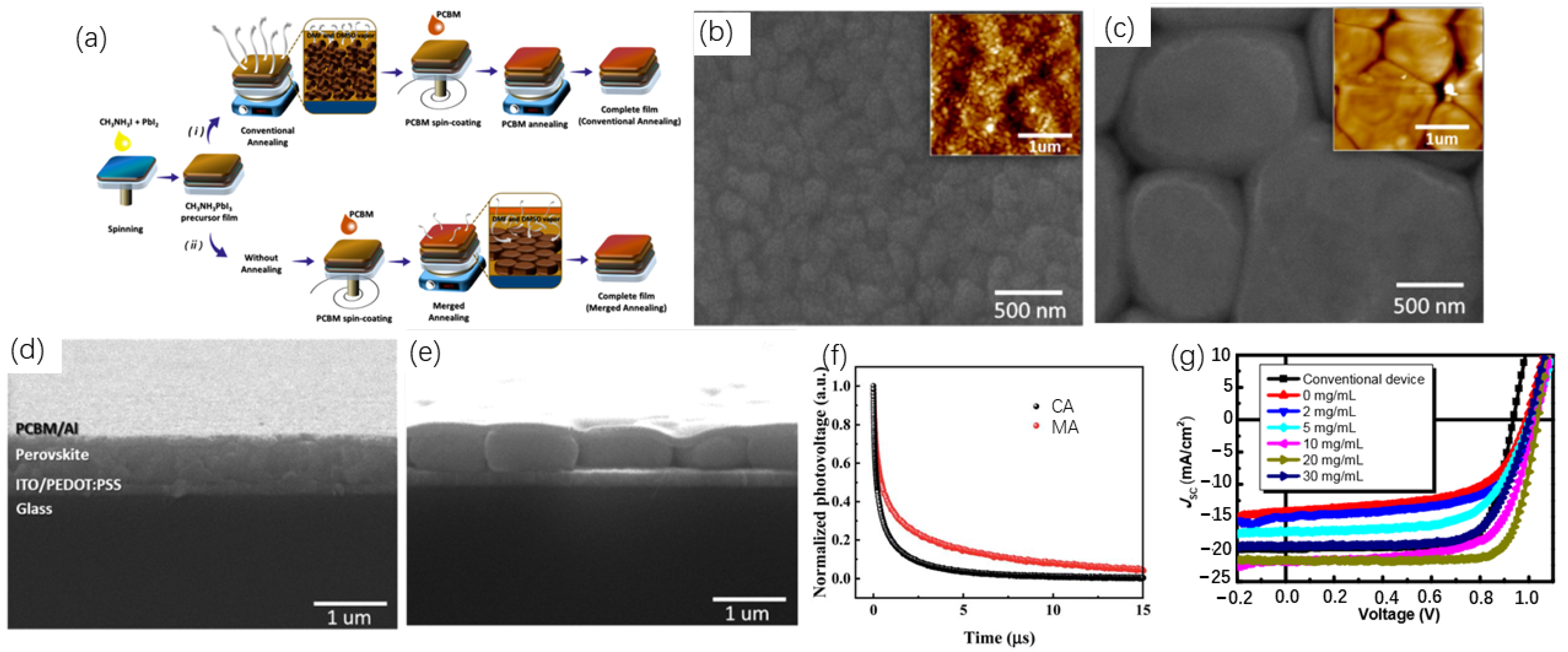
- Liu, Y.; Shin, I.; Hwang, I.-W.; Kim, S.; Lee, J.; Yang, M.-S.; Jung, Y.K.; Jang, J.-W.; Jeong, J.H.; Park, S.H.; et al. Single-Crystal-like Perovskite for High-Performance Solar Cells Using the Effective Merged Annealing Method. ACS Appl. Mater. Interfaces 2017, 9, 12382–12390. [Google Scholar] [CrossRef] [PubMed]
- Wu, H.; Lian, X.; Li, J.; Zhang, Y.; Zhou, G.; Wen, X.; Xie, Z.; Zhu, H.; Wu, G.; Chen, H. Merged interface construction toward ultra-low Voc loss in inverted two-dimensional Dion–Jacobson perovskite solar cells with efficiency over 18%. J. Mater. Chem. A 2021, 9, 12566–12573. [Google Scholar] [CrossRef]
- Lian, X.; Wu, H.; Zuo, L.; Zhou, G.; Wen, X.; Zhang, Y.; Wu, G.; Xie, Z.; Zhu, H.; Chen, H. Stable Quasi-2D Perovskite Solar Cells with Efficiency over 18% Enabled by Heat–Light Co-Treatment. Adv. Funct. Mater. 2020, 30, 2004188. [Google Scholar] [CrossRef]
- Zhou, L.; Chang, J.; Liu, Z.; Sun, X.; Lin, Z.; Chen, D.; Zhang, C.; Zhang, J.; Hao, Y. Enhanced Planar Perovskite Solar Cells Efficiency and Stability Using Perovskite/PCBM Heterojunction through One-Step Formation. Nanoscale 2018, 10, 3053–3059. [Google Scholar] [CrossRef]
- Butsriruk, K.; Passokorn, P.; Taychatanapat, T.; Chatraphorn, S. Surface treatment of PTAA hole transport layer for inverted perovskite solar cells. J. Phys. Conf. Ser. 2023, 2431, 012045. [Google Scholar] [CrossRef]
- Calió, L.; Kazim, S.; Grätzel, M.; Ahmad, S. Hole-Transport Materials for Perovskite Solar Cells. Angew Chem. Int. Ed. 2016, 55, 14522–14545. [Google Scholar] [CrossRef] [PubMed]
- Jiménez-González, A.E.; Cambray, J.G. Deposition of NiOx thin films by sol–gel technique. Surf. Eng. 2000, 16, 73–76. [Google Scholar] [CrossRef]
- Ghodsi, F.E.; Khayatiyan, S.A. Preparation and Determination of Optical Properties of NiO Thin Films Deposited by Dip Coating Technique. Surf. Rev. Lett. 2007, 14, 219–224. [Google Scholar] [CrossRef]
- Patil, V.P.; Pawar, S.; Chougule, M.; Godse, P.; Sakhare, R.; Sen, S.; Joshi, P. Effect of Annealing on Structural, Morphological, Electrical and Optical Studies of Nickel Oxide Thin Films. J. Surf. Eng. Mater. Adv. Technol. 2011, 1, 35–41. [Google Scholar] [CrossRef]
- Nalage, S.R.; Chougule, M.A.; Sen, S.; Joshi, P.B.; Patil, V.B. Sol–gel synthesis of nickel oxide thin films and their characterization. Thin Solid Films 2012, 520, 4835–4840. [Google Scholar] [CrossRef]
- Zorkipli, N.N.M.; Kaus, N.H.M.; Mohamad, A.A. Synthesis of NiO Nanoparticles through Sol-gel Method. Procedia Chem. 2016, 19, 626–631. [Google Scholar] [CrossRef]
- Kayani, Z.N.; Butt, M.Z.; Riaz, S.; Naseem, S. Synthesis of NiO nanoparticles by sol-gel technique. Mater. Sci. 2018, 36, 547–552. [Google Scholar] [CrossRef]
- Yin, X.; Guo, Y.; Xie, H.; Que, W.; Kong, L.B. Nickel Oxide as Efficient Hole Transport Materials for Perovskite Solar Cells. Sol. RRL 2019, 3, 1900001. [Google Scholar] [CrossRef]
- Park, I.J.; Kang, G.; Park, M.A.; Kim, J.S.; Seo, S.W.; Kim, D.H.; Zhu, K.; Park, T.; Kim, J.Y. Highly Efficient and Uniform 1 cm2 Perovskite Solar Cells with an Electrochemically Deposited NiOx Hole-Extraction Layer. ChemSusChem 2017, 10, 2660–2667. [Google Scholar] [CrossRef] [PubMed]
- Kim, H.-S.; Lee, C.-R.; Im, J.-H.; Lee, K.-B.; Moehl, T.; Marchioro, A.; Moon, S.-J.; Humphry-Baker, R.; Yum, J.-H.; Moser, J.E.; et al. Lead Iodide Perovskite Sensitized All-Solid-State Submicron Thin Film Mesoscopic Solar Cell with Efficiency Exceeding 9%. Sci. Rep. 2012, 2, 591. [Google Scholar] [CrossRef]
- Macdonald, T.J.; Batmunkh, M.; Lin, C.-T.; Kim, J.; Tune, D.D.; Ambroz, F.; Li, X.; Xu, S.; Sol, C.; Papakonstantinou, I.; et al. Origin of Performance Enhancement in TiO2-Carbon Nanotube Composite Perovskite Solar Cells. Small Methods 2019, 3, 1900164. [Google Scholar] [CrossRef]
- Fang, Y.; Wang, X.; Wang, Q.; Huang, J.; Wu, T. Impact of annealing on spiro-OMeTAD and corresponding solid-state dye sensitized solar cells: Impact of annealing on spiro-OMeTAD. Phys. Status Solidi A 2014, 211, 2809–2816. [Google Scholar] [CrossRef]
- Rombach, F.M.; Haque, S.A.; Macdonald, T.J. Lessons learned from spiro-OMeTAD and PTAA in perovskite solar cells. Energy Environ. Sci. 2021, 14, 5161–5190. [Google Scholar] [CrossRef]
- Zhao, X.; Kim, H.-S.; Seo, J.-Y.; Park, N.-G. Effect of Selective Contacts on the Thermal Stability of Perovskite Solar Cells. ACS Appl. Mater. Interfaces 2017, 9, 7148–7153. [Google Scholar] [CrossRef]
- Malinauskas, T.; Tomkute-Luksiene, D.; Sens, R.; Daskeviciene, M.; Send, R.; Wonneberger, H.; Jankauskas, V.; Bruder, I.; Getautis, V. Enhancing Thermal Stability and Lifetime of Solid-State Dye-Sensitized Solar Cells via Molecular Engineering of the Hole-Transporting Material Spiro-OMeTAD. ACS Appl. Mater. Interfaces 2015, 7, 11107–11116. [Google Scholar] [CrossRef]
- Mesquita, I.; Andrade, L.; Mendes, A. Temperature Impact on Perovskite Solar Cells Under Operation. ChemSusChem 2019, 12, 2186–2194. [Google Scholar] [CrossRef]
- Bailie, C.D.; Unger, E.L.; Zakeeruddin, S.M.; Grätzel, M.; McGehee, M.D. Melt-infiltration of spiro-OMeTAD and thermal instability of solid-state dye-sensitized solar cells. Phys. Chem. Chem. Phys. 2014, 16, 4864. [Google Scholar] [CrossRef]
- Wang, S.; Sina, M.; Parikh, P.; Uekert, T.; Shahbazian, B.; Devaraj, A.; Meng, Y.S. Role of 4- tert -Butylpyridine as a Hole Transport Layer Morphological Controller in Perovskite Solar Cells. Nano Lett. 2016, 16, 5594–5600. [Google Scholar] [CrossRef] [PubMed]
- Kasparavicius, E.; Magomedov, A.; Malinauskas, T.; Getautis, V. Long-Term Stability of the Oxidized Hole-Transporting Materials used in Perovskite Solar Cells. Chem. A Eur. J. 2018, 24, 9910–9918. [Google Scholar] [CrossRef] [PubMed]
- Heo, J.H.; Im, S.H.; Noh, J.H.; Mandal, T.N.; Lim, C.-S.; Chang, J.A.; Lee, Y.H.; Kim, H.; Sarkar, A.; Nazeeruddin, M.K.; et al. Efficient inorganic–organic hybrid heterojunction solar cells containing perovskite compound and polymeric hole conductors. Nat. Photon. 2013, 7, 486–491. [Google Scholar] [CrossRef]
- Ko, Y.; Kim, Y.; Lee, C.; Kim, Y.; Jun, Y. Investigation of Hole-Transporting Poly(triarylamine) on Aggregation and Charge Transport for Hysteresisless Scalable Planar Perovskite Solar Cells. ACS Appl. Mater. Interfaces 2018, 10, 11633–11641. [Google Scholar] [CrossRef]
- Sharif, R.; Khalid, A.; Ahmad, S.W.; Rehman, A.; Qutab, H.G.; Akhtar, H.H.; Mahmood, K.; Afzal, S.; Saleem, F. A comprehensive review of the current progresses and material advances in perovskite solar cells. Nanoscale Adv. 2023, 5, 3803–3833. [Google Scholar] [CrossRef]
- Bruening, K.; Tassone, C.J. Antisolvent processing of lead halide perovskite thin films studied by in situ X-ray diffraction. J. Mater. Chem. A 2018, 6, 18865–18870. [Google Scholar] [CrossRef]
- Chen, S.; Xiao, X.; Chen, B.; Kelly, L.L.; Zhao, J.; Lin, Y.; Toney, M.F.; Huang, J. Crystallization in one-step solution deposition of perovskite films: Upward or downward? Sci. Adv. 2021, 7, eabb2412. [Google Scholar] [CrossRef] [PubMed]
- Barrows, A.T.; Lilliu, S.; Pearson, A.J.; Babonneau, D.; Dunbar, A.D.F.; Lidzey, D.G. Monitoring the Formation of a CH3 NH3 PbI 3–x Clx Perovskite during Thermal Annealing Using X-Ray Scattering. Adv. Funct. Mater. 2016, 26, 4934–4942. [Google Scholar] [CrossRef]
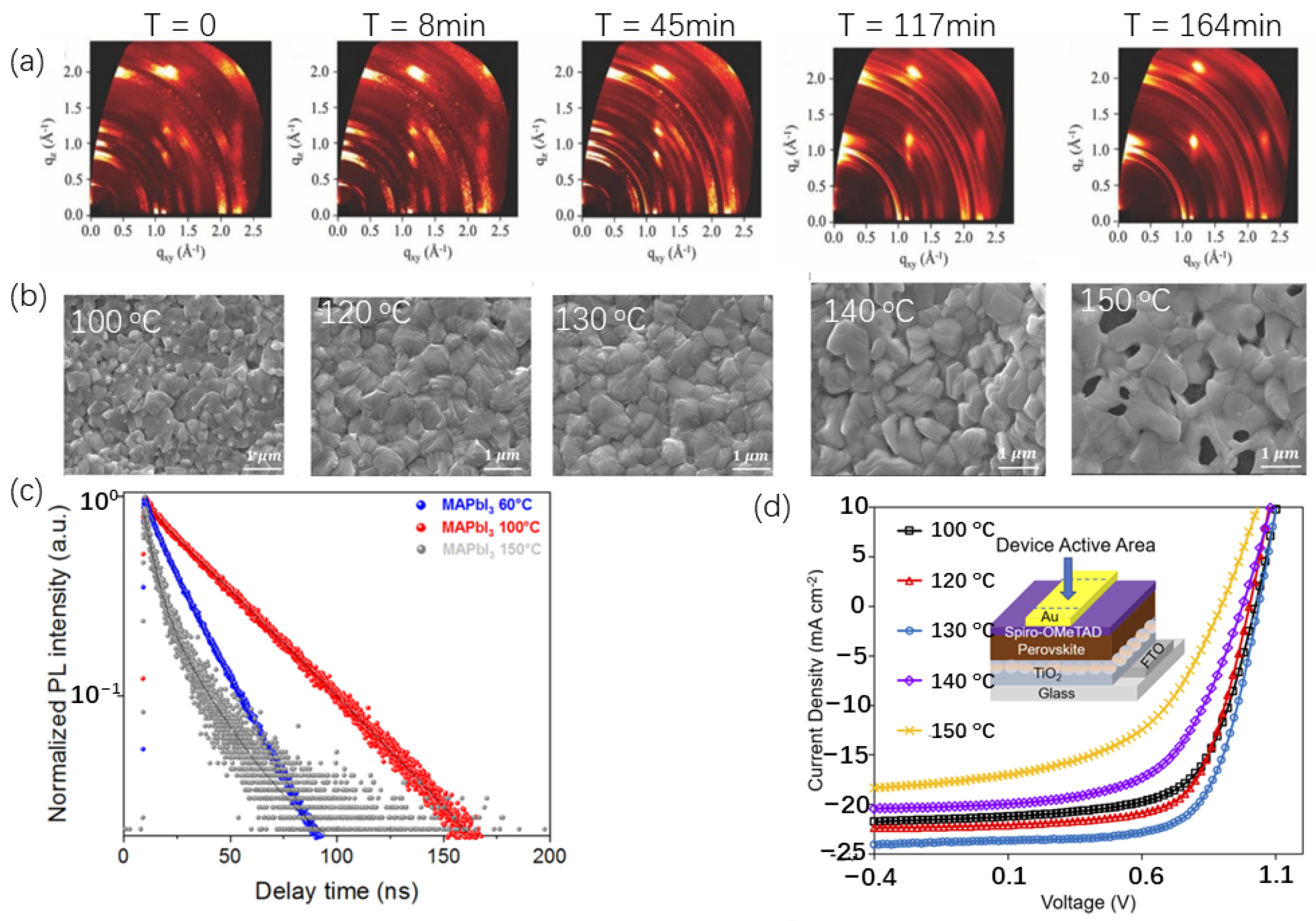
- Oyewole, D.O.; Koech, R.K.; Ichwani, R.; Ahmed, R.; Hinostroza Tamayo, J.; Adeniji, S.A.; Cromwell, J.; Colin Ulloa, E.; Oyewole, O.K.; Agyei-Tuffour, B.; et al. Annealing effects on interdiffusion in layered FA-rich perovskite solar cells. AIP Adv. 2021, 11, 065327. [Google Scholar] [CrossRef]
- Ali Akhavan Kazemi, M.; Jamali, A.; Sauvage, F. A Holistic Study on the Effect of Annealing Temperature and Time on CH3NH3PbI3-Based Perovskite Solar Cell Characteristics. Front. Energy Res. 2021, 9, 732886. [Google Scholar] [CrossRef]
- Chiang, C.-H.; Tseng, Z.-L.; Wu, C.-G. Planar heterojunction perovskite/PC 71 BM solar cells with enhanced open-circuit voltage via a (2/1)-step spin-coating process. J. Mater. Chem. A 2014, 2, 15897–15903. [Google Scholar] [CrossRef]
- Jeon, N.J.; Noh, J.H.; Yang, W.S.; Kim, Y.C.; Ryu, S.; Seo, J.; Seok, S.I. Compositional engineering of perovskite materials for high-performance solar cells. Nature 2015, 517, 476–480. [Google Scholar] [CrossRef] [PubMed]
- Zhao, X.; Liu, T.; Kaplan, A.B.; Yao, C.; Loo, Y.-L. Accessing Highly Oriented Two-Dimensional Perovskite Films via Solvent-Vapor Annealing for Efficient and Stable Solar Cells. Nano Lett. 2020, 20, 8880–8889. [Google Scholar] [CrossRef] [PubMed]
- Sã, S. Flash infrared annealing as a cost-effective and low environmental impact processing method for planar perovskite solar cells. Mater. Today 2019, 31, 39–46. [Google Scholar]
- Lavery, B.W.; Kumari, S.; Konermann, H.; Draper, G.L.; Spurgeon, J.; Druffel, T. Intense Pulsed Light Sintering of CH 3 NH 3 PbI 3 Solar Cells. ACS Appl. Mater. Interfaces 2016, 8, 8419–8426. [Google Scholar] [CrossRef]
- Zheng, Z.-H.; Lan, H.-B.; Su, Z.-H.; Peng, H.-X.; Luo, J.-T.; Liang, G.-X.; Fan, P. Single Source Thermal Evaporation of Two-dimensional Perovskite Thin Films for Photovoltaic Applications. Sci. Rep. 2019, 9, 17422. [Google Scholar] [CrossRef]
- Li, B.; Jiu, T.; Kuang, C.; Ma, S.; Chen, Q.; Li, X.; Fang, J. Chlorobenzene vapor assistant annealing method for fabricating high quality perovskite films. Org. Electron. 2016, 34, 97–103. [Google Scholar] [CrossRef]
- Li, Y.; Chen, J.; Cai, P.; Wen, Z. An electrochemically neutralized energy-assisted low-cost acid-alkaline electrolyzer for energy-saving electrolysis hydrogen generation. J. Mater. Chem. A 2018, 6, 4948–4954. [Google Scholar] [CrossRef]
- You, P.; Li, G.; Tang, G.; Cao, J.; Yan, F. Ultrafast laser-annealing of perovskite films for efficient perovskite solar cells. Energy Environ. Sci. 2020, 13, 1187–1196. [Google Scholar] [CrossRef]
- Ghahremani, A.H.; Martin, B.; Gupta, A.; Bahadur, J.; Ankireddy, K.; Druffel, T. Rapid fabrication of perovskite solar cells through intense pulse light annealing of SnO2 and triple cation perovskite thin films. Mater. Des. 2020, 185, 108237. [Google Scholar] [CrossRef]
- Chen, Q.; Ma, T.; Wang, F.; Liu, Y.; Liu, S.; Wang, J.; Cheng, Z.; Chang, Q.; Yang, R.; Huang, W.; et al. Rapid Microwave-Annealing Process of Hybrid Perovskites to Eliminate Miscellaneous Phase for High Performance Photovoltaics. Adv. Sci. 2020, 7, 2000480. [Google Scholar] [CrossRef] [PubMed]
- Wang, K.-L.; Zhang, C.-C.; Jiang, Y.-R.; Liu, H.-R.; Li, X.-M.; Jain, S.M.; Ma, H. High-quality perovskite films via post-annealing microwave treatment. New J. Chem. 2019, 43, 9338–9344. [Google Scholar] [CrossRef]
- Hua, J.; Deng, X.; Niu, C.; Huang, F.; Peng, Y.; Li, W.; Ku, Z.; Cheng, Y. A pressure-assisted annealing method for high quality CsPbBr 3 film deposited by sequential thermal evaporation. RSC Adv. 2020, 10, 8905–8909. [Google Scholar] [CrossRef]
- Martin, B.; Yang, M.; Bramante, R.C.; Amerling, E.; Gupta, G.; Van Hest, M.F.A.M.; Druffel, T. Fabrication of flexible perovskite solar cells via rapid thermal annealing. Mater. Lett. 2020, 276, 128215. [Google Scholar] [CrossRef]
- Dong, G.; Yang, Y.; Sheng, L.; Xia, D.; Su, T.; Fan, R.; Shi, Y.; Wang, J. Inverted thermal annealing of perovskite films: A method for enhancing photovoltaic device efficiency. RSC Adv. 2016, 6, 44034–44040. [Google Scholar] [CrossRef]
- Li, N.; Niu, X.; Li, L.; Wang, H.; Huang, Z.; Zhang, Y.; Chen, Y.; Zhang, X.; Zhu, C.; Zai, H.; et al. Liquid medium annealing for fabricating durable perovskite solar cells with improved reproducibility. Science 2021, 373, 561–567. [Google Scholar] [CrossRef]
- Eze, V.O.; Seike, Y.; Mori, T. Synergistic Effect of Additive and Solvent Vapor Annealing on the Enhancement of MAPbI3 Perovskite Solar Cells Fabricated in Ambient Air. ACS Appl. Mater. Interfaces 2020, 12, 46837–46845. [Google Scholar] [CrossRef]
- Sun, X.; Zhang, C.; Chang, J.; Yang, H.; Xi, H.; Lu, G.; Chen, D.; Lin, Z.; Lu, X.; Zhang, J.; et al. Mixed-solvent-vapor annealing of perovskite for photovoltaic device efficiency enhancement. Nano Energy 2016, 28, 417–425. [Google Scholar] [CrossRef]
- Chin, S.-H.; Choi, J.W.; Woo, H.C.; Kim, J.H.; Lee, H.S.; Lee, C.-L. Realizing a highly luminescent perovskite thin film by controlling the grain size and crystallinity through solvent vapour annealing. Nanoscale 2019, 11, 5861–5867. [Google Scholar] [CrossRef] [PubMed]
- Yuan, B.; Zhao, S.; Xu, Z.; Song, D.; Qiao, B.; Li, Y.; Qin, Z.; Meng, J.; Xu, X. Improving the photovoltaic performance of planar heterojunction perovskite solar cells by mixed solvent vapor treatment. RSC Adv. 2018, 8, 11574–11579. [Google Scholar] [CrossRef] [PubMed]
- Luo, J.; Qiu, R.Z.; Yang, Z.S.; Wang, Y.X.; Zhang, Q.F. Mechanism and effect of γ-butyrolactone solvent vapor post-annealing on the performance of a mesoporous perovskite solar cell. RSC Adv. 2018, 8, 724–731. [Google Scholar] [CrossRef]
- Serafini, P.; Boix, P.P.; Barea, E.M.; Edvinson, T.; Sánchez, S.; Mora-Seró, I. Photonic Processing of MAPbI 3 Films by Flash Annealing and Rapid Growth for High-Performance Perovskite Solar Cells. Solar RRL 2022, 6, 2200641. [Google Scholar] [CrossRef]
- Sanchez, S.; Hua, X.; Phung, N.; Steiner, U.; Abate, A. Flash Infrared Annealing for Antisolvent-Free Highly Efficient Perovskite Solar Cells. Adv. Energy Mater. 2018, 8, 1702915. [Google Scholar] [CrossRef]
- Sanchez, S.; Christoph, N.; Grobety, B.; Phung, N.; Steiner, U.; Saliba, M.; Abate, A. Efficient and Stable Inorganic Perovskite Solar Cells Manufactured by Pulsed Flash Infrared Annealing. Adv. Energy Mater. 2018, 8, 1802060. [Google Scholar] [CrossRef]
- Murugadoss, G.; Thangamuthu, R.; Rajesh Kumar, M.; Sakkarapalayam Murugesan, S.K.; Prabu, V. Air free fast solution annealing method for perovskite solar cells. Mater. Lett. 2017, 205, 130–133. [Google Scholar] [CrossRef]
- Zhi, L.; Li, Y.; Cao, X.; Li, Y.; Cui, X.; Ci, L.; Wei, J. Dissolution and recrystallization of perovskite induced by N-methyl-2-pyrrolidone in a closed steam annealing method. J. Energy Chem. 2019, 30, 78–83. [Google Scholar] [CrossRef]
- Francisco-López, A.; Charles, B.; Weber, O.J.; Alonso, M.I.; Garriga, M.; Campoy-Quiles, M.; Weller, M.T.; Goñi, A.R. Equal Footing of Thermal Expansion and Electron–Phonon Interaction in the Temperature Dependence of Lead Halide Perovskite Band Gaps. J. Phys. Chem. Lett. 2019, 10, 2971–2977. [Google Scholar] [CrossRef] [PubMed]
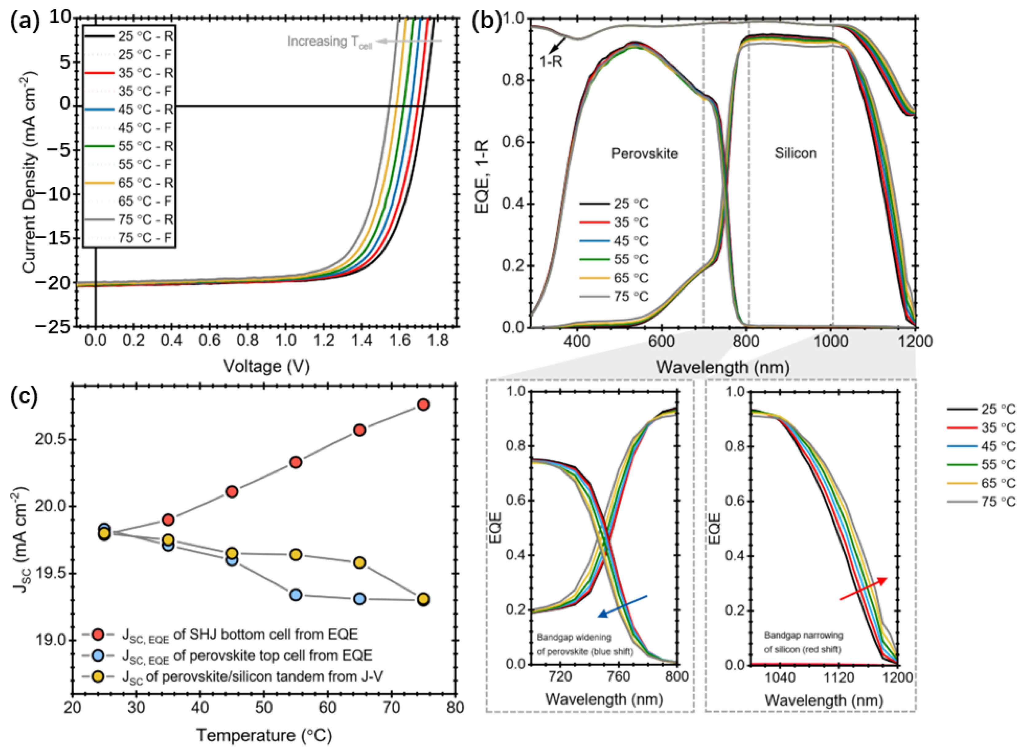
- Aydin, E.; Allen, T.G.; De Bastiani, M.; Xu, L.; Ávila, J.; Salvador, M.; Van Kerschaver, E.; De Wolf, S. Interplay between temperature and bandgap energies on the outdoor performance of perovskite/silicon tandem solar cells. Nat. Energy 2020, 5, 851–859. [Google Scholar] [CrossRef]
- Yuan, Y.; Chae, J.; Shao, Y.; Wang, Q.; Xiao, Z.; Centrone, A.; Huang, J. Photovoltaic Switching Mechanism in Lateral Structure Hybrid Perovskite Solar Cells. Adv. Energy Mater. 2015, 5, 1500615. [Google Scholar] [CrossRef]
- Wu, X.; Wu, B.; Zhu, Z.; Tayyab, M.; Gao, D. Importance and Advancement of Modification Engineering in Perovskite Solar Cells. Solar RRL 2022, 6, 2200171. [Google Scholar] [CrossRef]
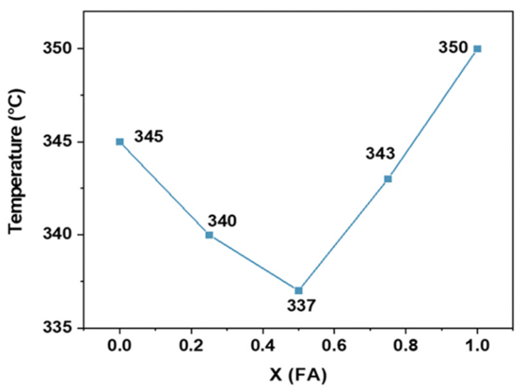
- Chen, Z.; Yang, Z.; Du, S.; Lin, D.; Zhang, F.; Zeng, Y.; Liu, G.; Nie, Z.; Ma, L. Thermal stability and decomposition kinetics of mixed-cation halide perovskites. Phys. Chem. Chem. Phys. 2023, 25, 32966–32971. [Google Scholar] [CrossRef]
- Bush, K.A.; Palmstrom, A.F.; Yu, Z.J.; Boccard, M.; Cheacharoen, R.; Mailoa, J.P.; McMeekin, D.P.; Hoye, R.L.Z.; Bailie, C.D.; Leijtens, T.; et al. 23.6%-efficient monolithic perovskite/silicon tandem solar cells with improved stability. Nat. Energy 2017, 2, 17009. [Google Scholar] [CrossRef]
- Bush, K.A.; Bailie, C.D.; Chen, Y.; Bowring, A.R.; Wang, W.; Ma, W.; Leijtens, T.; Moghadam, F.; McGehee, M.D. Thermal and Environmental Stability of Semi-Transparent Perovskite Solar Cells for Tandems Enabled by a Solution-Processed Nanoparticle Buffer Layer and Sputtered ITO Electrode. Adv. Mater. 2016, 28, 3937–3943. [Google Scholar] [CrossRef]
- Fu, F.; Feurer, T.; Weiss, T.P.; Pisoni, S.; Avancini, E.; Andres, C.; Buecheler, S.; Tiwari, A.N. High-efficiency inverted semi-transparent planar perovskite solar cells in substrate configuration. Nat. Energy 2016, 2, 16190. [Google Scholar] [CrossRef]
- Mariotti, S.; Jäger, K.; Diederich, M.; Härtel, M.S.; Li, B.; Sveinbjörnsson, K.; Kajari-Schröder, S.; Peibst, R.; Albrecht, S.; Korte, L.; et al. Monolithic Perovskite/Silicon Tandem Solar Cells Fabricated Using Industrial p-Type Polycrystalline Silicon on Oxide/Passivated Emitter and Rear Cell Silicon Bottom Cell Technology. Solar RRL 2022, 6, 2101066. [Google Scholar] [CrossRef]
- Kuwano, K.; Ashok, S. Investigation of sputtered indium-tin oxide/silicon interfaces: Ion damage, hydrogen passivation and low-temperature anneal. Appl. Surf. Sci. 1997, 117, 629–633. [Google Scholar] [CrossRef]
- Liu, J.; De Bastiani, M.; Aydin, E.; Harrison, G.T.; Gao, Y.; Pradhan, R.R.; Eswaran, M.K.; Mandal, M.; Yan, W.; Seitkhan, A.; et al. Efficient and stable perovskite-silicon tandem solar cells through contact displacement by MgFx. Science 2022, 377, 302–306. [Google Scholar] [CrossRef] [PubMed]
- Ono, L.K.; Raga, S.R.; Wang, S.; Kato, Y.; Qi, Y. Temperature-dependent hysteresis effects in perovskite-based solar cells. J. Mater. Chem. A 2015, 3, 9074–9080. [Google Scholar] [CrossRef]
- Ishii, T.; Otani, K.; Takashima, T.; Kawai, S. Estimation of the maximum power temperature coefficients of PV modules at different time scales. Sol. Energy Mater. Sol. Cells 2011, 95, 386–389. [Google Scholar] [CrossRef]
- Liu, S.H.; Simburger, E.J.; Matsumoto, J.; Garcia, A.; Ross, J.; Nocerino, J. Evaluation of thin-film solar cell temperature coefficients for space applications. Prog. Photovolt. 2005, 13, 149–156. [Google Scholar] [CrossRef]
- Habisreutinger, S.N.; Leijtens, T.; Eperon, G.E.; Stranks, S.D.; Nicholas, R.J.; Snaith, H.J. Carbon Nanotube/Polymer Composites as a Highly Stable Hole Collection Layer in Perovskite Solar Cells. Nano Lett. 2014, 14, 5561–5568. [Google Scholar] [CrossRef] [PubMed]
- Ava, T.T.; Al Mamun, A.; Marsillac, S.; Namkoong, G. A Review: Thermal Stability of Methylammonium Lead Halide Based Perovskite Solar Cells. Appl. Sci. 2019, 9, 188. [Google Scholar] [CrossRef]
- Bruno, A.; Cortecchia, D.; Chin, X.Y.; Fu, K.; Boix, P.P.; Mhaisalkar, S.; Soci, C. Temperature and Electrical Poling Effects on Ionic Motion in MAPbI 3 Photovoltaic Cells. Adv. Energy Mater. 2017, 7, 1700265. [Google Scholar] [CrossRef]
- Yuan, Y.; Huang, J. Ion Migration in Organometal Trihalide Perovskite and Its Impact on Photovoltaic Efficiency and Stability. Acc. Chem. Res. 2016, 49, 286–293. [Google Scholar] [CrossRef]
- Jošt, M.; Lipovšek, B.; Glažar, B.; Al-Ashouri, A.; Brecl, K.; Matič, G.; Magomedov, A.; Getautis, V.; Topič, M.; Albrecht, S. Perovskite Solar Cells go Outdoors: Field Testing and Temperature Effects on Energy Yield. Adv. Energy Mater. 2020, 10, 2000454. [Google Scholar] [CrossRef]
- Bhandari, S.; Mallick, T.K.; Sundaram, S. Enlightening the temperature coefficient of triple mesoscopic CH 3 NH 3 PbI 3−x Cl x/NiO and double mesoscopic CsFAMAPbI3−x Brx/CuSCN carbon perovskite solar cells. J. Phys. Energy 2023, 5, 025006. [Google Scholar] [CrossRef]
- Khenkin, M.V.; Katz, E.A.; Abate, A.; Bardizza, G.; Berry, J.J.; Brabec, C.; Brunetti, F.; Bulović, V.; Burlingame, Q.; Di Carlo, A.; et al. Consensus statement for stability assessment and reporting for perovskite photovoltaics based on ISOS procedures. Nat. Energy 2020, 5, 35–49. [Google Scholar] [CrossRef]


| Scan Direction | Mesoporous Layer | JSC (mA cm−2) | VOC (V) | Fill Factor | PCE (%) |
|---|---|---|---|---|---|
| Forward −0.1 V | Brookite TiO2 | 20.2 ± 0.6 | 0.98 ± 0.01 | 0.69 ± 0.01 | 13.5 ± 0.6 |
| ↓a | Anatase TiO2 | 19.4 ± 1.4 | 0.87 ± 0.01 | 0.62 ± 0.01 | 10.3 ± 0.7 |
| 1.1 V | Al2O3 | 19.2 ± 1.3 | 1.05 ± 0.02 | 0.55 ± 0.03 | 11.0 ± 0.8 |
| Backward 1.1 V | Brookite TiO2 | 20.0 ± 0.6 | 0.99 ± 0.01 | 0.67 ± 0.03 | 13.3 ± 1.0 |
| ↓ | Anatase TiO2 | 19.4 ± 1.4 | 0.90 ± 0.01 | 0.66 ± 0.01 | 11.5 ± 0.6 |
| −0.1 V | Al2O3 | 18.5 ± 1.6 | 1.05 ± 0.02 | 0.66 ± 0.05 | 12.7 ± 0.3 |
| Method | Device Structure | Maintained Initial PCE a | References | |
|---|---|---|---|---|
| Solvent-vapor annealing | IPA | FTO/c-TiO2/m-TiO2/(BDA)(Cs0.1FA0.9)4Pb5I16/dopant-free ST1/Cr/Au. | C:13.9%, | [97] |
| M:18.9% | ||||
| CB | ITO/PEDOT:PSS/perovskite/PCBM/Al | C:11.86% | [101] | |
| M:13.40% | ||||
| DMSO | ITO/PEDOT:PSS/MAPbI3/PCBM/Ag | C:3.40% | [111] | |
| M:17.04% | ||||
| IPA:DMF = 100:1 | ITO/PEDOT:PSS/MAPbI3/PCBM/Ag | C:11.5% | [112] | |
| M:14.3% | ||||
| Water | N\A | N\A | [113] | |
| Hac/CB | ITO/PEDOT:PSS/MAPbI3/PCBM/Ag | C:11.44% | [114] | |
| M:12.80% | ||||
| GBL | ITO/TiO2/MAPbI3/spiro-OMeTAD)/Au | C:13.05% | [115] | |
| M16.85% | ||||
| Laser irradiation | Flash infrared annealing | ITO/TiO2/MAPbI3/spiro-OMeTAD)/Au | C:18.3% | [98] |
| M:18.1% | ||||
| FTO/TiO2/TiO2-mesoporous/MAPbI3/Spiro/Au | N\A | [116] | ||
| M19.5% | ||||
| FTO/TiO2/perovskite/Spiro/Au | C:19.0% | [117] | ||
| M:19.2% | ||||
| FTO/TiO2/CsPbI1.5Br1.5/PTAA/Au | N\A | [118] | ||
| M:10.3% | ||||
| Laser annealing | FTO/TiO2/perovskite/Spiro/Au | C:18.10% | [103] | |
| M:20.98% | ||||
| Intense pulsed light sintering | FTO/TiO2/perovskite/Spiro/Au | C:8.21% | [99] | |
| M:11.5% | ||||
| Microwave treatment | ITO/PEDOT:PSS/perovskite/BCP/PCBM/Au | C:11.58% | [106] | |
| M:13.39% | ||||
| ITO/PTAA/perovskite/PCBM/C60/BCP/Ag | C:18.33 | [105] | ||
| M:18.59 | ||||
| Pressure-assisted annealing | FTO/c-TiO2/CsPbBr3/Carbon | C:2.79% | [107] | |
| M:7.22% | ||||
| Air-free fast solution | FTO/bl-TiO2/m-TiO2/MAPbI3/Spiro/Au | N\A | [119] | |
| M:12.10% | ||||
| Closed steam annealing method | FTO/TiO2/MAPbI3/Spiro/Au | C:12.35% | [120] | |
| 13.77% | ||||
| Rapid thermal annealing | PET/ITO/PTAA/PFN/PVSK/C60/BCP/Ag | N\A | [108] | |
| M:14.58% | ||||
| Inverted thermal annealing | FTO/c- TiO2/MAPbI3/HTM/Au | C:10.89% | [109] | |
| M:12.88% | ||||
| Liquid medium annealing | ITO/SnO2/FA1-x-yMAxCsyPbI3-zBrz/SpiroOMeTAD/Au | C:23.15% | [110] | |
| M:24.04% | ||||
| Merged annealing method | ITO/PEDOT:PSS/perovskite/PCBM/Al | C:11.93% | [63] | |
| M:18.27% | ||||
Disclaimer/Publisher’s Note: The statements, opinions and data contained in all publications are solely those of the individual author(s) and contributor(s) and not of MDPI and/or the editor(s). MDPI and/or the editor(s) disclaim responsibility for any injury to people or property resulting from any ideas, methods, instructions or products referred to in the content. |
© 2024 by the authors. Licensee MDPI, Basel, Switzerland. This article is an open access article distributed under the terms and conditions of the Creative Commons Attribution (CC BY) license (https://creativecommons.org/licenses/by/4.0/).
Share and Cite
Wu, S.; Li, C.; Lien, S.Y.; Gao, P. Temperature Matters: Enhancing Performance and Stability of Perovskite Solar Cells through Advanced Annealing Methods. Chemistry 2024, 6, 207-236. https://doi.org/10.3390/chemistry6010010
Wu S, Li C, Lien SY, Gao P. Temperature Matters: Enhancing Performance and Stability of Perovskite Solar Cells through Advanced Annealing Methods. Chemistry. 2024; 6(1):207-236. https://doi.org/10.3390/chemistry6010010
Chicago/Turabian StyleWu, Shengcong, Chi Li, Shui Yang Lien, and Peng Gao. 2024. "Temperature Matters: Enhancing Performance and Stability of Perovskite Solar Cells through Advanced Annealing Methods" Chemistry 6, no. 1: 207-236. https://doi.org/10.3390/chemistry6010010