Article

Application the Ion Beam Sputtering Deposition Technique for the Development of Spin-Wave Structures on Ferroelectric Substrates

by
Sergei A. Sharko
1,*,
Aleksandra I. Serokurova
1,
Nikolay N. Novitskii
1,
Valerii A. Ketsko
2 and
Alexandre I. Stognij
1
1
Scientific-Practical Materials Research Centre NAS of Belarus, 19 P. Brovki Street, 220072 Minsk, Belarus
2
Kurnakov Institute of General and Inorganic Chemistry, Russian Academy of Sciences, Leninskii Pr. 31, Moscow 119991, Russia
*
Author to whom correspondence should be addressed.
Ceramics 2023, 6(3), 1415-1433; https://doi.org/10.3390/ceramics6030087
Submission received: 9 June 2023 / Revised: 30 June 2023 / Accepted: 3 July 2023 / Published: 5 July 2023

Abstract

:
The microwave properties of structures in the form of the 2 μm iron-yttrium garnet (YIG) films, grown by the ion beam sputtering deposition method on epitaxially mismatched substrates of ferroelectric ceramics based on lead zirconate titanate (PZT, PbZr0.45Ti0.55O3), are discussed. The obtained structures were formed and pre-smoothed by the ion beam planarization substrates with the use of an anti-diffusion layer of titanium dioxide TiO2. The atomic force microscopy showed that the planarization of the substrates allows for reaching a nanoscale level of roughness (up to 10 nm). The presence of smooth plane–parallel interfaces of YIG/TiO2 and TiO2/PZT is evidenced by scanning electron microscopy performed in focused gallium ion beams. Ferromagnetic resonance spectroscopy revealed a broadening in the absorption line of the ferrite garnet layers in the resonance ≈ 100 Oe. This broadening is associated with the presence of defects caused by the of the ceramic substrate non-ideality. The estimated damping coefficient of spin waves turned out to be ~10−3, which is two orders of magnitude higher than in an ideal YIG single crystal. The YIG/TiO2/PZT structures obtained can be used for the study of spin waves.

1. Introduction

The transition from electric charges to spin waves [1,2,3,4] opens up new possibilities for the transmission, processing, and storage of information using devices operating in the microwave region (from 0.3 to 300 GHz). The advantages of spin waves are low propagation losses, as well as low phase and group velocities, which make it possible to implement a wide variety of microwave devices (filters, delay lines, as well as magneto-optical information storage and processing devices, etc.). The traditional method of electronic control, associated with changing the magnitude of the magnetic field with the help of currents in the electromagnet coils, is associated with high energy consumption and large installation sizes. Another control method is carried out by changing the electric field. For its implementation, composite structures can be used, in which magnetic and electrical ordering is combined. The use of ferroelectric (FE) [5] and piezoelectric (PE) [2,6] layers as part of these structures makes it possible to control the performance of microwave devices by means of external electric and magnetic fields [2,7].
In this regard, composite layered structures based on garnet ferrites thin films on ferroelectric and piezoelectric ceramic substrates are of great interest. Yttrium iron garnet Y3Fe5O12 (YIG) [1,8,9,10] is one of the best-known spin-wave materials [5,11,12,13]. This is largely due to the fact that in the single-crystal state, it is characterized by the very weak damping of spin waves [9,14,15] (the Gilbert damping parameter α is 3.0 × 10⁻⁵), high transparency, and very high rotation coefficient values of plane polarized light (magnetooptical Faraday effect) [16] in a wide spectral range. In addition, it is characterized by low dielectric losses, high resistivity, and an extremely narrow ferromagnetic resonance linewidth (ΔH = 0.2 Oe) [9,15]. All this led to the extensive use of YIG in the manufacturing of microwave devices [12,13,17].
Lead zirconate titanate (PZT, PbZrxTi1−xO3) ferroelectric ceramics [18,19,20,21] have high residual polarization values (1–4 nC/cm2) and low-enough temperatures (550–650 °C) for the perovskite phase formation [22]. This inspired its wide use; for example, for the magnetoelectric effect [20,21,22] achievement in layered inhomogeneous structures in the form of ferromagnetic (FM) layers on FE and PE substrates.
The obtaining of high-quality epitaxial YIG films on gadolinium gallium garnet (Gd3Ga5O12, GGG) substrates by the most commonly used method of liquid-phase epitaxy does not cause any particular problems due to a slight mismatch between the parameters of their crystal lattices (aYIG = 12.376 Å [9,10,23,24], aGGG = 12.383 Å [23], Δa/a ≈ 6 × 10⁻⁴). However, to implement the principles of spin-wave electronic structures controlled by external magnetic and electric fields, it is necessary to obtain layers of garnet ferrites on imperfect substrates of FE ceramic materials. The latter faces a number of difficulties. First, during the polycrystalline ceramic materials synthesis, a great deal of cavities appear in the volume of the substance because of the loose fit of crystallites to each other [25]. Secondly, a significant mismatch of crystal lattices (Δa/a ≈ 0.67) does not allow epitaxial growth. Finally, the root-mean-square surface roughness of ceramic materials is very high and can be of tenths and units of micrometers. All of the above problems are solved by using special processing methods.
The high-quality layered structure formation requires the existence of a flat FM layer/FE substrate interface due to the strong adhesion of the layer to the substrate [26]. In most cases, ferromagnet/ferroelectric layered structures are formed by mechanical, for example, adhesive bonding of FM and FE layers [4,27]. The substantial drawback of such structures is the unfeasibility of using microelectronic methods (for instance, liquid and dry etching) for their processing. Furthermore, the difference in thermal expansion coefficients leads to the destruction of structures under thermal exposure. The creation of such an interface was shown in our works to be carried out using the method of ion beam planarization [28,29,30] of the PZT substrate surface relief. Strengthening the adhesive bond between materials allows for increasing the area of layer/substrate direct contact.
YIG films synthesized on silicon and quartz substrates are characterized by low structural perfection because of the differences in their crystal lattice parameters and thermal expansion coefficients [31,32]. Nevertheless, when preparing Co/TiO2 structures by ion beam sputtering deposition on Si and GaAs substrates [33], the possibility, in principle, to obtain high-quality polycrystalline YIG films by means of a titanium dioxide TiO2 antidiffusion layer was shown. The availability of this layer between YIG and PZT should provide the separation of the deposition and crystallization processes of the garnet ferrite layer and exclude the secondary chemical reactions throughout annealing. Simultaneously, the chemical indifference of the substrate with respect to the layer deposited during crystallization is kept. The amorphous TiO2 layer separates the YIG and PZT crystal layers from each other so that their lattices do not touch. Due to this, there is a significant reduction or complete suppression of internal stresses caused by a crystallographic parameters mismatching at the film/substrate interface. This prevents the layered structures degradation due to the deformations occurring in them at higher temperatures.
In this work, it is shown that the application of ion beam planarization of the surface of FE substrates based on PZT ceramics using a submicron-thick antidiffusion layer of titanium dioxide TiO2 and subsequent deposition of yttrium iron garnet Y3Fe5O12 layer ensures the obtaining of a high-quality spin-wave structure Y3Fe5O12 (2 µm)/TiO2 (0.2 µm)/PZT (400 µm). This structure is characterized by a high homogeneity of ferrimagnetic layers on non-epitaxial PZT ceramic substrates.

2. Materials and Methods

2.1. Materials and Methods of Obtaining

The standard method of solid-phase reactions for the synthesis of the ceramic PZT substrates of PbZr0.45Ti0.55O3 composition including the operations of grinding and hot pressing was used [34,35]. This composition is closest to the boundary of the morphotropic phase transition, where the FE properties are most pronounced. The oxides PbO, ZrO2 and TiO2 were taken in the required weight ratio in terms of cations and thoroughly mixed. The resulting mixtures were triturated manually in an agate mortar for 15–20 min with the addition of a small amount of ethanol. Before weighing, the oxides were annealed in air at 1000 °C for 2 h at a constant weight to remove moisture and adsorbed substances. Preliminary firing of the mixtures was carried out in air at 1100 °C for 4 h, followed by their grinding in a ball mill. The mixtures thus obtained were pressed in a hydraulic press in steel molds at a pressure of 108 Pa. The final synthesis was carried out in air at 1550 °C for 5 h. The samples were quenched from 1000 °C to room temperature to obtain compositions with an oxygen content close to stoichiometric.
Then, the initial substrates were thinned to a thickness of 400 µm by sequentially changing emery and polishing mixtures during mechanical grinding. Finishing mechanochemical polishing was carried out using diamond powder in a natural wax medium. As a result, the level of surface roughness was brought up to tenths of a micrometer. After mechanochemical treatment, the ceramic was a low-porosity material in the form of a conglomerate of randomly oriented single-crystal blocks with a crystallographic faceting and with an average grain size in the range of 1–2 µm (Figure 1a).
The substrates were treated with a sequence of two or three microwave pulses with a power of 400 W in low-pressure oxygen plasma (50–150 Pa) to destroy unsaturated chemical bonds on the surface of the substrates and to remove impurities. The microwave oven operates at a frequency of 2.45 GHz, which corresponds to a photon energy of ≈1 meV. With such energy, thermal destruction of long molecules of organic impurities, for example, fats, which prevent the formation of an adhesive bond between the substrate and the growing film, occurs. They burn out in an oxygen atmosphere and are removed from the surface in the form of final volatile low-molecular products.
The samples after mechanochemical treatment were subjected to two-stage ion beam planarization [28,29,30] to ensure nanoscale surface roughness of PZT substrate and to form an antidiffusion titanium dioxide layer on it. At the first stage, a layer of TiO2 with a thickness of ≈0.2 μm was deposited onto the substrate by sputtering a titanium target with oxygen ions with an energy of 1.6 keV and an ion current density of 0.25 mA/cm2. The deposition rate of the antidiffusion layer was 0.2 μm/h. Surface depressions were predominantly filled during the TiO2 layer deposition. The second stage was accompanied by sputtering of the surface with an antidiffusion layer by the same ions with an energy of 0.4 keV over a time slightly longer than the time of TiO2 layer formation. Sputtering was carried out at a rate of 0.8 μm/h by an O+ ion beam with an energy of 0.4 keV and a current density of 0.2 mA/cm2. The angular dependence of the sputtering yield led to a more intense sputtering of surface protrusions than flat areas. This caused a smoothing of the surface relief as a whole. The double repetition of deposition sputtering cycles during planarization provided a nanoscale level of roughness [25].
Two competing processes occur when the PZT surface is ion beam sputtered during planarization: surface smoothing due to the removal of small relief protrusions and the opening of subsurface cavities (Figure 1b). The latter are formed in places of loose contact between crystallites at the stage of ceramic sintering. Their presence significantly hinders the achievement of nanometer-scale smoothness of the PZT surface [25].
The formation of the YIG layer on the PZT substrate surface was carried out as a result of the sputtering of the corresponding garnet ferrite target with a diameter of 76 mm by a flow of argon and oxygen ions with a current density of 0.2 mA/cm2 and an energy of 1.5 keV. The ferrimagnet material was optimally sputtered at an oxygen concentration in the gas mixture of 10%. The deposition rate was 0.3 μm/h and the layer thickness was 2 μm. The deposition process was carried out at room temperature and pressure in the working chamber of 2.5 × 10⁻² Pa. The resulting amorphous YIG layer was crystallized by annealing at 820 °C in the air atmosphere for 5 min [34].
The planarization of the PZT substrate surface relief, as well as the deposition of a garnet ferrite layer, were carried out by means of the double ion beam sputtering deposition setup. The latter was equipped with wide-aperture ion sources with a cold hollow cathode based on a two-stage self-sustained low-pressure discharge [36].

2.2. Methods of Research

X-ray diffraction patterns of samples were obtained on a Bruker D8 Advance diffractometer (Ettlingen, Germany, 2013) in the angle range 2θ 20–80°. Kα copper radiation at a wavelength of 1.5406 Å was used. X-ray fluorescence analysis was made on the characteristic radiation of the Am-241 isotope to determine the elemental composition of the structures obtained.
The surface and cross sections of the heterostructures obtained were analyzed using a scanning electron-ion microscope Helios NanoLab 600 (FEI Company, Hillsboro, OR, USA). Cross sections were built in gallium ion-focused beams with an energy of 32 keV. Atomic force microscopy (AFM) based on a scanning probe microscope NanoEducator was used to study the surface of the obtained samples in the contact mode. Magnetic force microscopy (MFM) was applied to reveal the relationship between structural inhomogeneities and magnetic defects on the surface by visualizing cylindrical magnetic domains in a perpendicular magnetic field. The vibrating sample magnetometer ‘Liquid Helium Free High Field Measurement System (Cryogenic Ltd., London, UK)’ was involved to perform magnetic measurements at room temperature in the magnetic field range of ±0.4 T (±4 kOe).
An ER-200 X-band electron paramagnetic resonance spectrometer (Bruker) was used to study ferromagnetic resonance (FMR). The studies were carried out at room temperature at a frequency of 9.45 GHz with longitudinal and transverse resonance excitation. In the first case, the external magnetic field was applied along the YIG ferrimagnetic layer surface, and in the second case, respectively, perpendicular to it. A curve of the first derivative of the absorption intensity with respect to the magnetic field strength dI/dH was plotted for four different-sized areas of one sample.

3. Results and Discussion
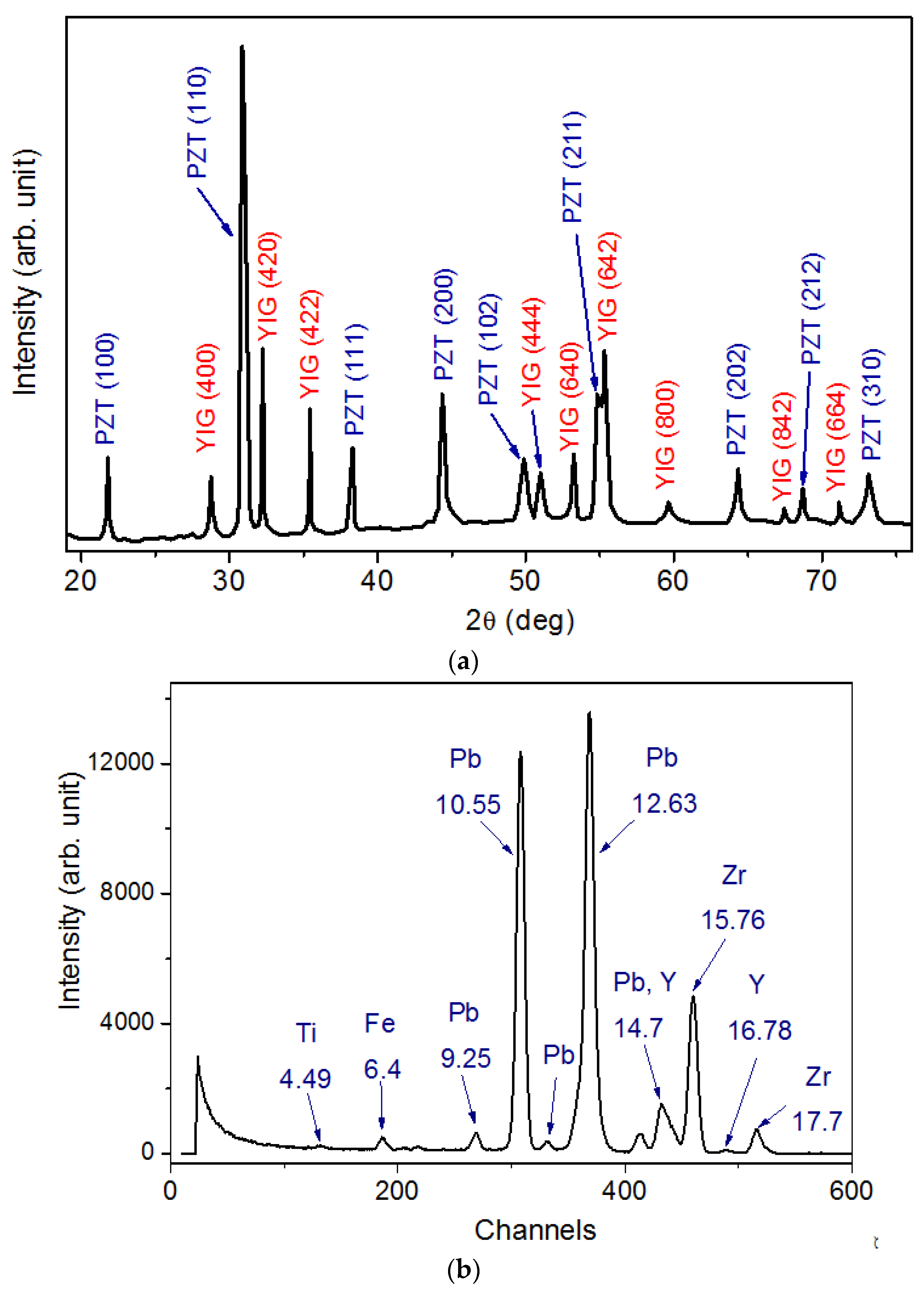
3.1. X-ray Studies

The X-ray diffraction pattern of the Y3Fe5O12 (2 µm)/TiO2 (0.2 µm)/PZT (400 µm) heterostructure sample shows all the main reflections of both the YIG ferrimagnetic layer and the FE of the PZT substrate (Figure 2a). The ordered set of YIG reflections corresponds to a cubic lattice [37] with a parameter of 12.378 Å, which is slightly larger than that for the corresponding bulk YIG single crystal (12.376 Å [9,10,23,24]). The expansion of the crystal lattice is due to both the influence of a certain amount of intrinsic impurities and the non-epitaxial mechanism of growth of the ferrite garnet layer on individual disordered ceramic grains. In this case, adhesion plays a decisive role in the formation of the structure on the substrate.
For the epitaxial growth of a layer on a substrate, two important conditions must be satisfied. The first condition is related to the matching of the crystal–chemical characteristics of the materials of the mating layers. In particular, the lattice parameters should not differ by more than 10%. The second condition is related to the local morphology of the substrate surface. If the first of them imposes fundamental restrictions on the possibility of epitaxial growth of a layer on a substrate, then the second one is not so strict and allows for the possibility of quasi-epitaxial growth only in separate small areas—the surfaces of single-crystal grains of the substrate oriented at some small angle to the growth plane. As for our structures, the parameter mismatch significantly exceeds the limit of the oriented growth existence, which prohibits their epitaxial matching in direct contact with the substrate. On the other hand, the presence of an intermediate amorphous TiO2 layer also makes this impossible.
Relative distortions in the crystal lattice parameters, calculated by the formula
Δa/a = −cot θ Δθ,
do not exceed 1% (Table 1). It is difficult to explain such small distortions Δa/a by a large amount of impurities introduced into the YIG lattice. This gives grounds to assume that the garnet ferrite layer is formed without diffusion [38] during ion beam deposition.
With a large mismatch between the YIG (aYIG = 12.376 Å) and PZT (aPZT = 4.139 Å [29]) crystal lattice parameters, the existence of both non-epitaxial polycrystalline and epitaxial single-crystal YIG/PZT structures is impossible when the crystal lattices of both materials are in direct contact. However, the presence of an amorphous TiO2 layer between the YIG and PZT layers leads to their separation, and therefore, the destruction of the structure does not occur.
The study of the elemental composition of the YIG/TiO2/PZT structure, performed by means of X-ray fluorescence analysis, established the correspondence of the elements to its main components Y3Fe5O12, TiO2, and PbZr0.45Ti0.55O3 (Figure 2b).

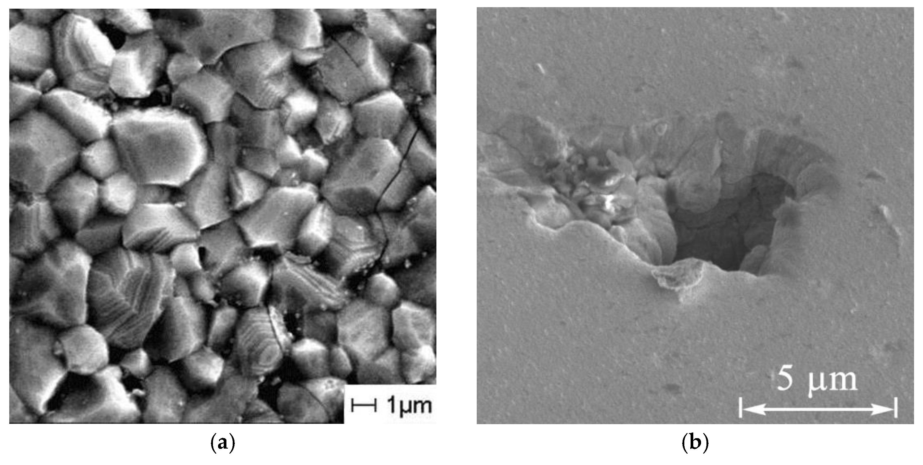
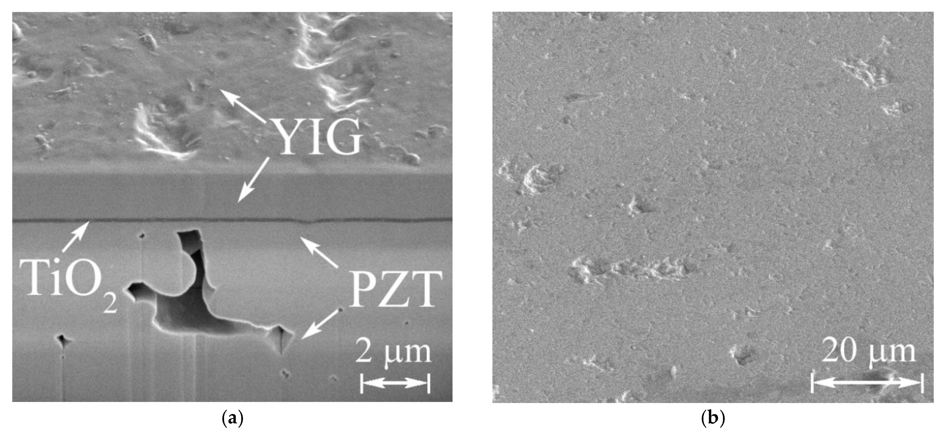
3.2. SEM Studies of the Cross Section

A continuous dark band of 0.2 µm thick titanium dioxide layer TiO2 in the cross section image (Figure 3a) of the heterostructure separates the upper YIG layer from the PZT substrate. The absence of X-ray reflections of the TiO2 layer in the diffraction pattern (Figure 2a) may indicate both its amorphous state and a small amount of the material forming it. In the latter case, the surface morphology of the components separated by it should not be changed significantly. The solid solution of PZT ceramics includes TiO2 oxide, along with zirconium ZrO2 and lead PbO oxides; therefore, the TiO2 buffer layer does not form foreign chemical compounds between the ferrimagnetic layer and the substrate, and neither change the physical properties of these layers. This is evidenced by the absence of delaminations and swelling between the ferrimagnetic layer and the substrate as well as the presence of a strong adhesive bond between the layers. All this leads to the appearance of smooth plane-parallel lower (TiO2/PZT) and upper (YIG/TiO2) interfaces in the YIG/TiO2/PZT heterostructure without any defects associated with the interaction between the buffer layer and the substrate (Figure 3a).
The hidden irregularly shaped cavities with typical dimensions of more than 1 μm are visible on the cross section of the substrate (Figure 3a). They remain after solid-phase synthesis and are the result of loose joining along the faces of randomly oriented substrate crystallites. The presence of such cavities, which are not eliminated even during planarization, leads to the depression formation with a characteristic depth of about 1 µm on the surface of the growing YIG layer (Figure 3b). In addition, small protrusions are also visible on the surface, the number of which significantly exceeds the number of depressions. Ion beam planarization occurs under conditions of the sputtering yield’s dependence upon the angle of the bombarding ions incidence. As a result, the largest relief projections are removed, and the aforementioned subsurface cavities are opened, forming depressions. Therefore, the number of the latter during ion beam planarization remains the same on average, while the height of the protrusions gradually decreases.

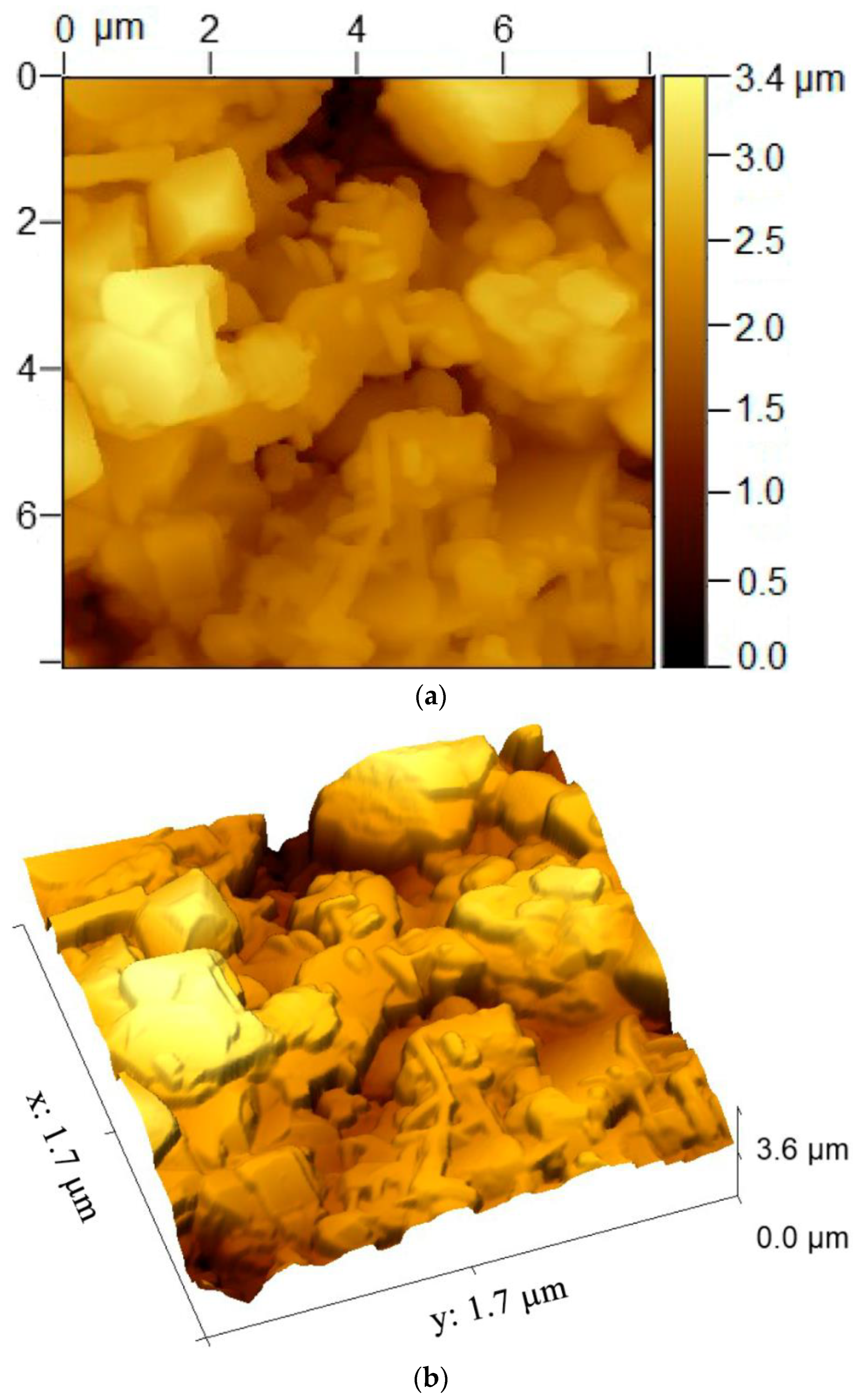
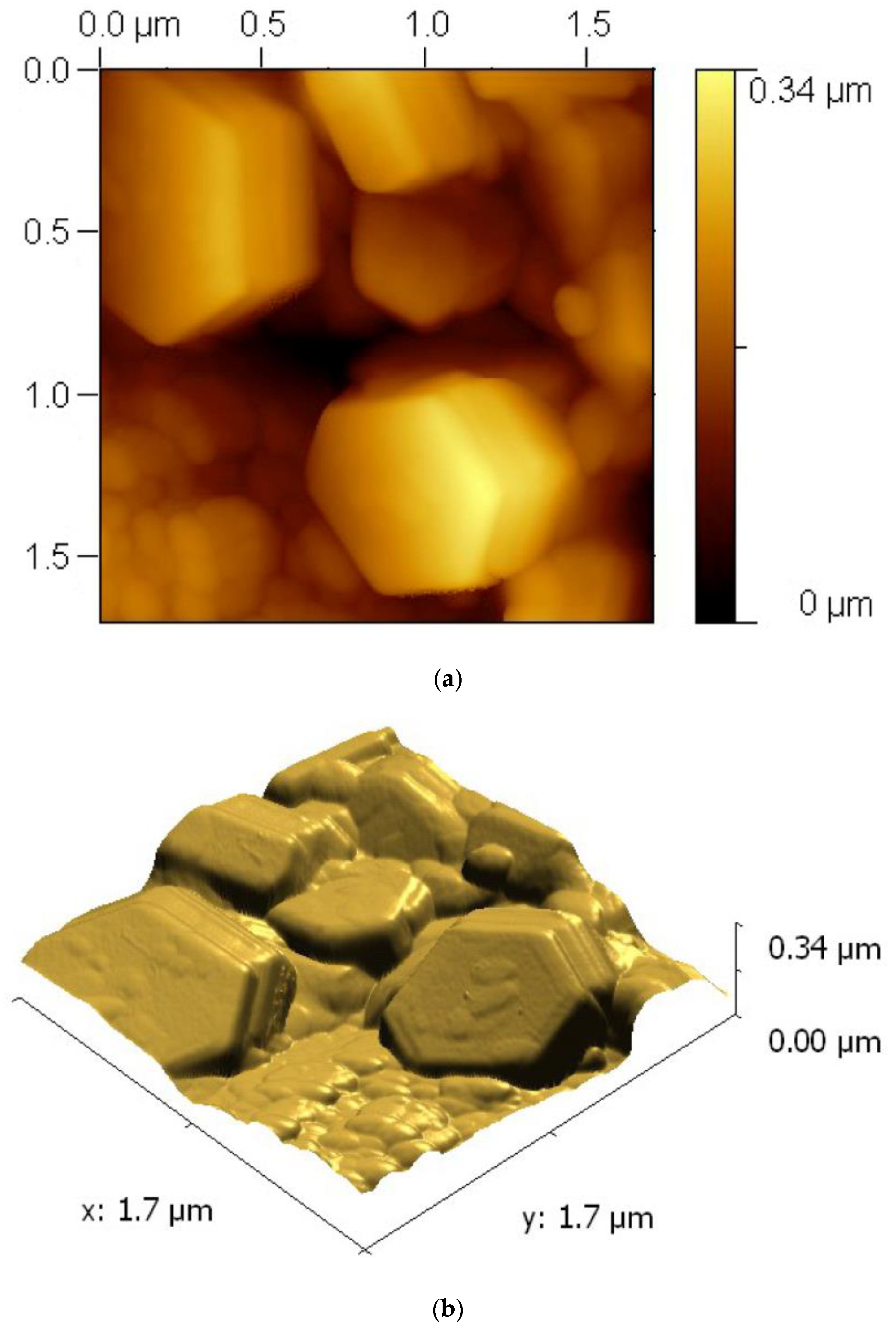
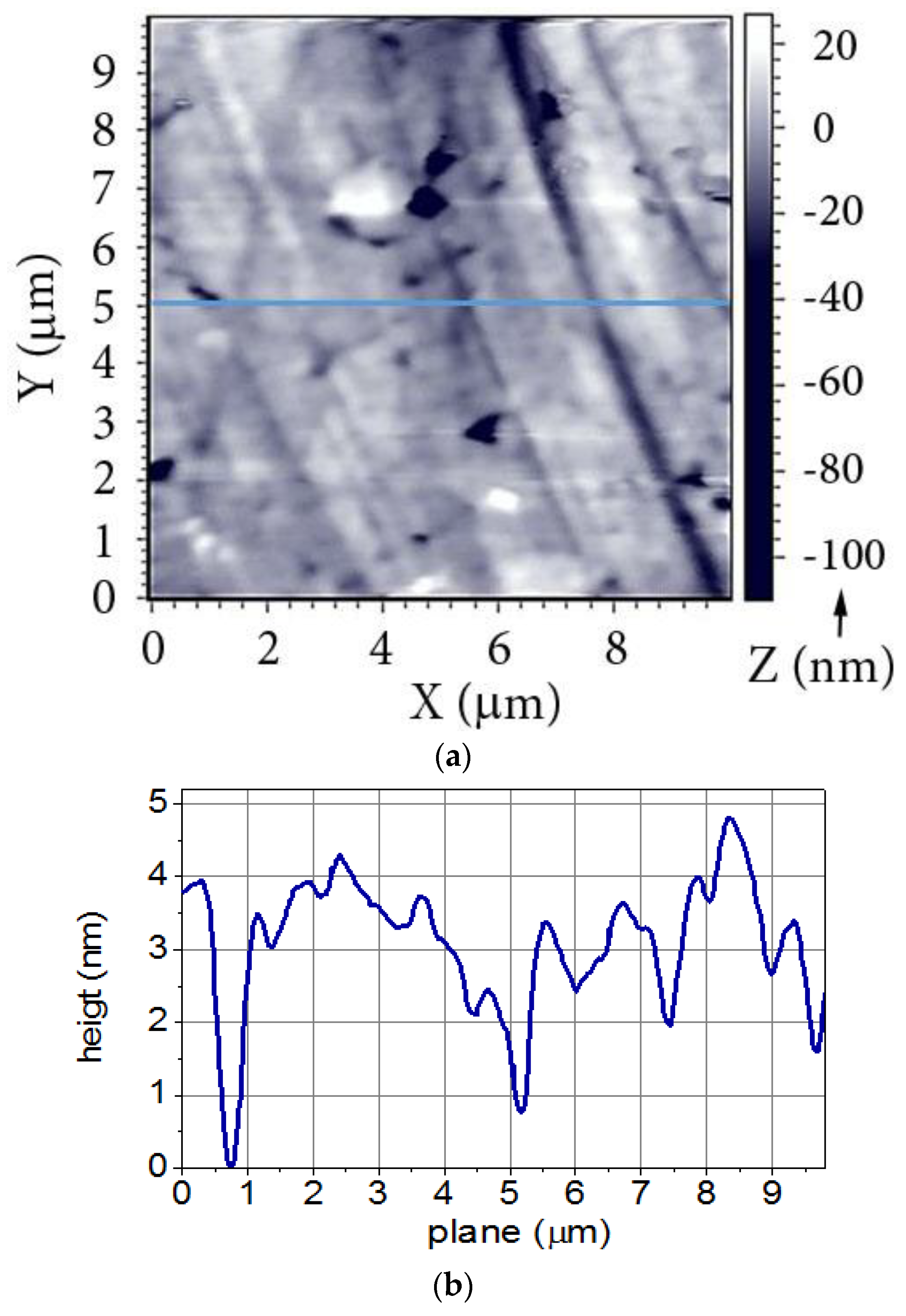
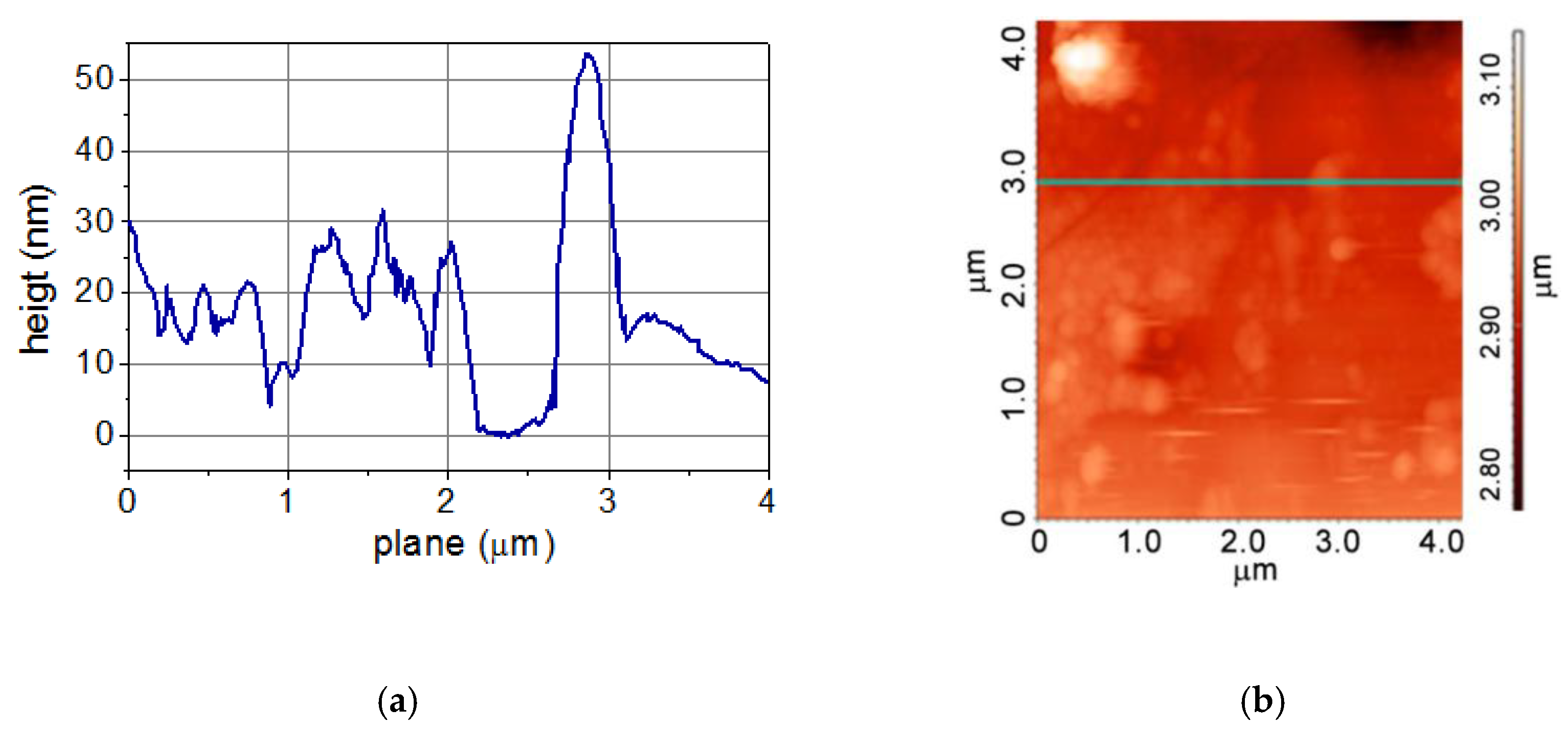
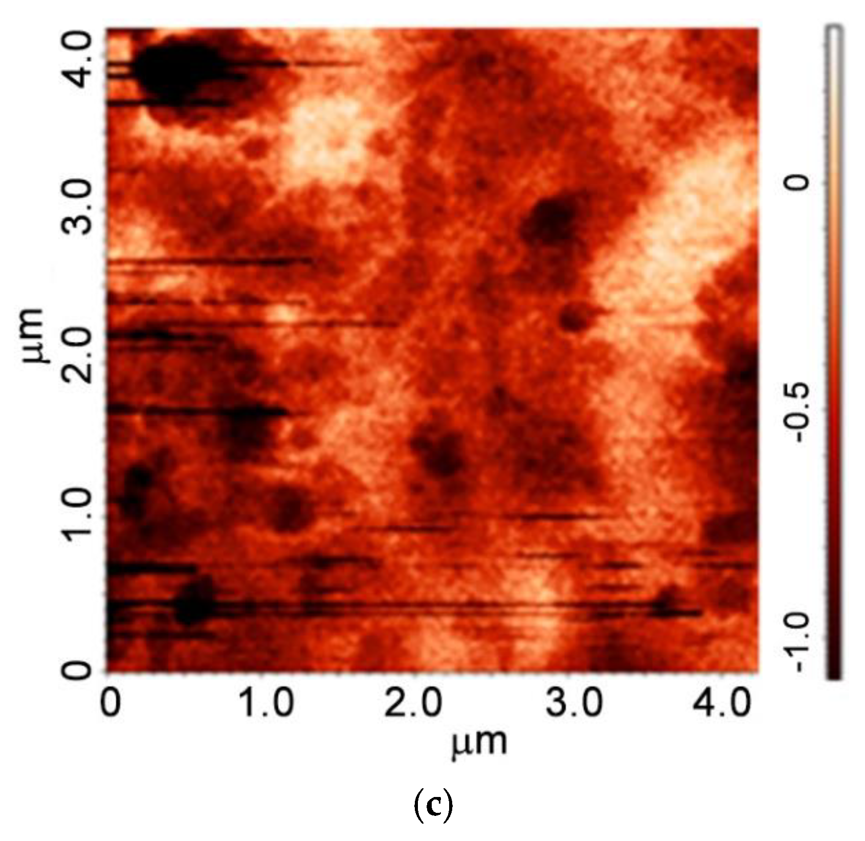
3.3. AFM Studies of Surface Morphology

AFM methods give insight into the changes that occur with the surface under ion beam exposure. In general, there is an improvement in the quality of the PZT substrate surface. The absolute height difference before the ion beam planarization of the substrate exceeded 3 μm (Figure 4). Dark areas on the AFM images (Figure 4) correspond to the above-mentioned near-surface cavities. The picture changes after ion beam planarization (Figure 5): the surface relief becomes smoother, and the substrate surface acquires a plane-parallel form. Crystallites obtain a pronounced hexagonal shape, and their faces become parallel to the growth surface, with a small angular dispersion relative to it. Open cavities remain on the surface, but their position changes during planarization, because they are closed in some places due to redeposition of the planarizing layer material into them while they are opened in others.
The state of the substrate surface is inherited by the overlying layer of garnet ferrite, as evidenced by the agreement between the results of SEM and AFM studies. The value of the maximum protrusions and depressions on the ferrite garnet surface in the YIG/TiO2/PZT heterostructure is no more than 35 nm (Figure 6), the number of which does not exceed 20% by area. The root-mean-square roughness at a base length of 4 µm along the horizontal AFM line (Figure 7a) is 9.7 nm. This is much smaller than the typical grain crystallite size of the initial PbZr0.45Ti0.55O3 ceramic substrate (Figure 1a). Comparison of these parameters is quite correct, since the edge protrusions of the crystallites of ceramic materials and the places of their joining, which extend beyond the surface plane, are the main relief-forming factors of the surface that determine its morphological features.
Comparison of our results with other works gives one the right to assert that the surface quality of the structures obtained by us is good. For example, YIG films with a thickness of 700 nm, obtained in [1] by the method of pulsed laser deposition, were characterized by the root-mean-square roughness Rq on silicon of 7.7 nm and less than 1 nm on GGG. YIG films 530 nm thick on amorphous quartz substrates were obtained by using the same method in [23], as well as obtained by synthesis from the liquid phase (chemical solution deposition) 300 nm thick on silicon substrates and annealed at 750–850 °C in [32]. The root-mean-square roughness for the former was 0.96–2.84 nm, while for the latter it turned out to be 4–6.5 nm. In thinner films of yttrium iron garnet (20 nm), obtained in [39] by chemical solution deposition on oxidized silicon substrates and annealed at 800 °C, Rq reached a subnanoscale value of 0.2 nm. These results are not unexpected, since they were obtained on sufficiently smooth substrates with a regular surface.

3.4. MFM Studies

Individual cylindrical magnetic domains in the form of dark rounded areas associated with transverse magnetization are noticeably distinguished in the MFM image (Figure 7c) of the YIG ferrimagnetic layer surface. These regions are due to the magnetic defects contained in them, which slow down the domain wall’s motion during magnetization. A higher coercivity, compared to the surrounding areas of the film, makes it difficult for them to remagnetize, and they remain unremagnetized, while the film as a whole is remagnetized to saturation in the opposite direction. The relationship between structural inhomogeneities and magnetic defects is most clearly indicated when comparing the MFM image (Figure 7c) with the AFM image (Figure 7b) of the same surface area. Light and dark areas of approximately the same shape in these figures complement each other in contrast.

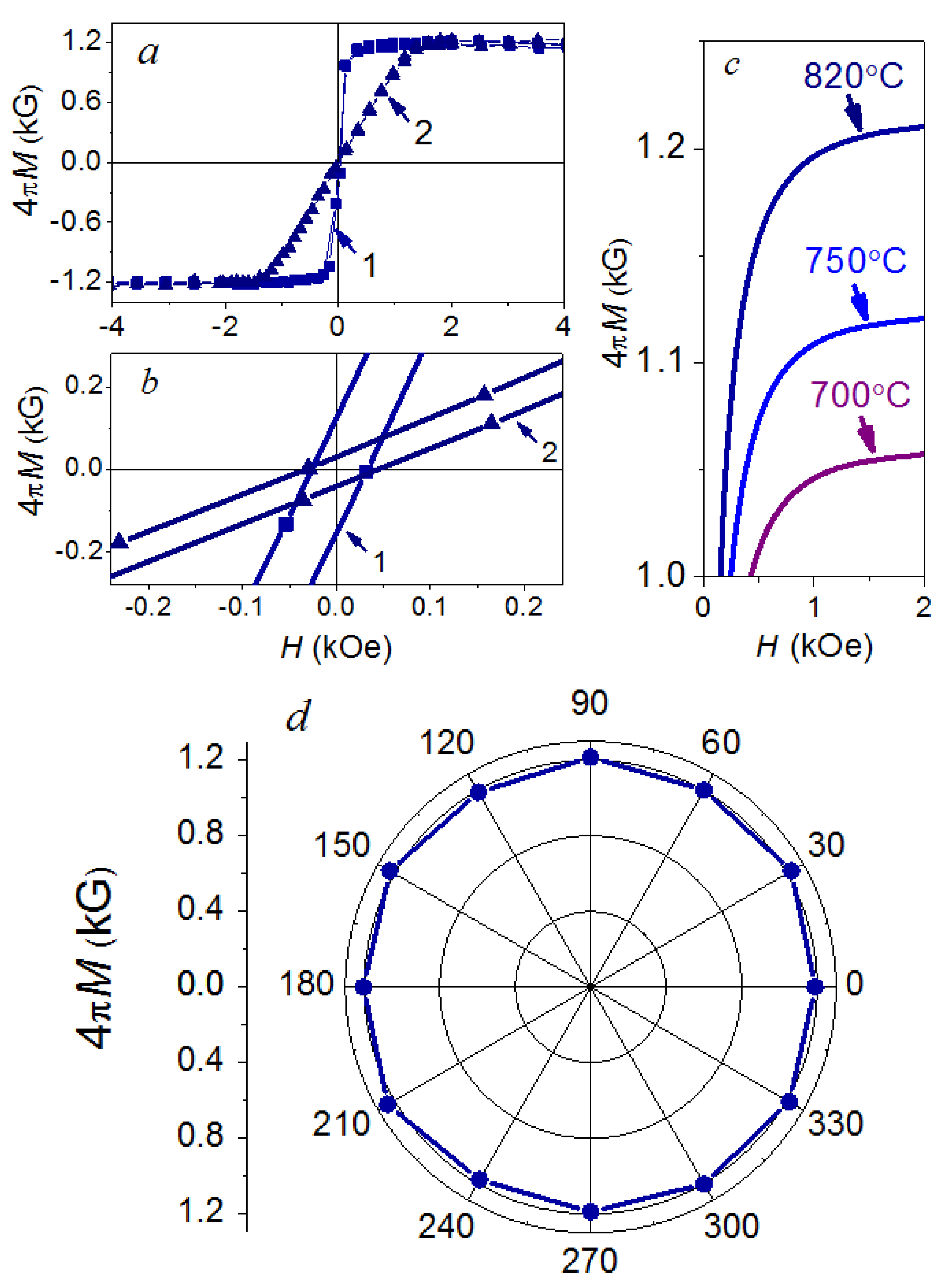
3.5. Magnetic Studies
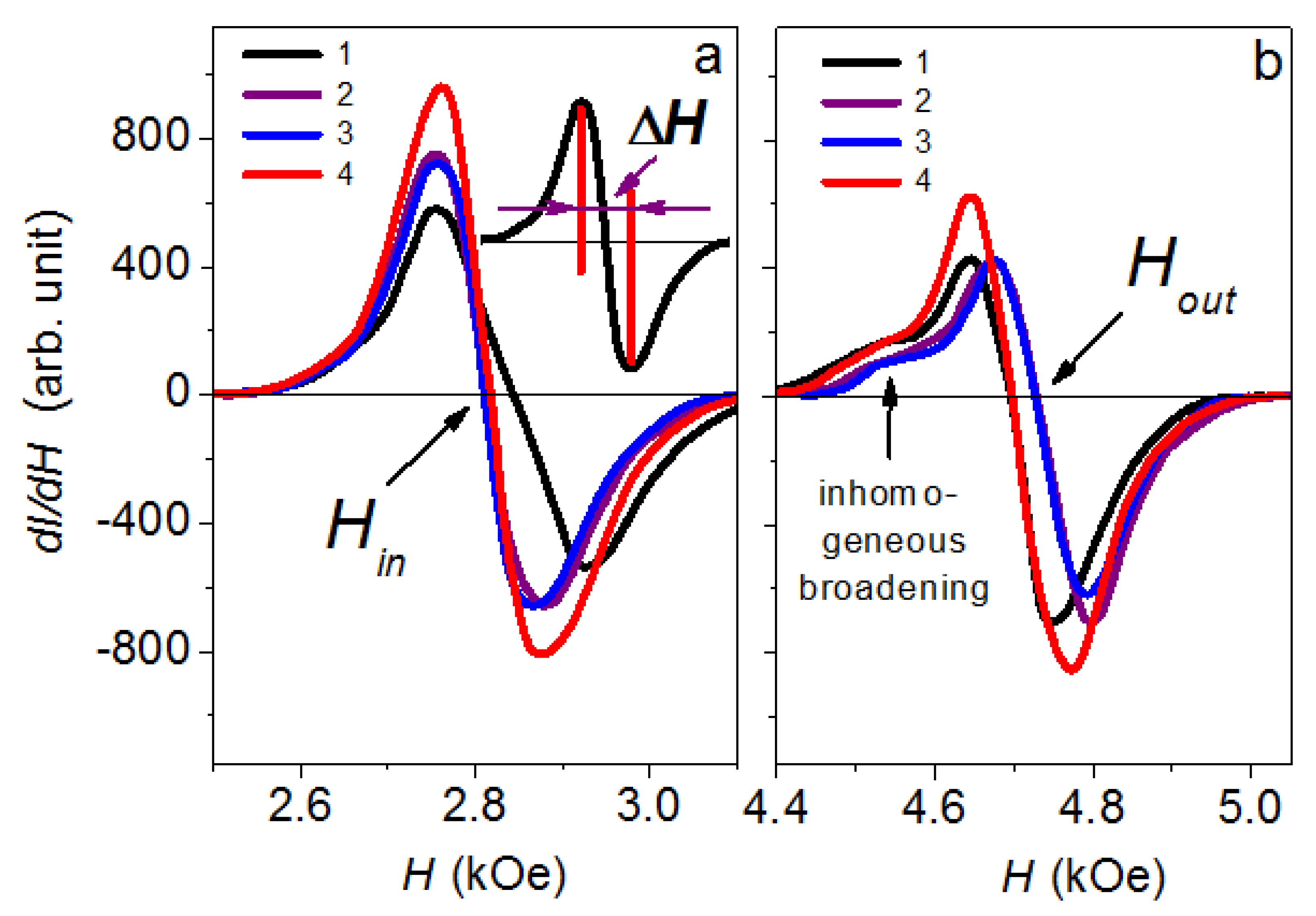
The saturation magnetization MS of 2 µm YIG layers on a planarized PZT substrate is approximately 1.2 kG (Figure 8a,b) after annealing in air at 820 °C, which reaches ≈0.7 of the MS of a massive YIG single crystal (1.75 kG at room temperature [9,10,23,32,40,41,42]). This indicates that the resulting layers are closest in stoichiometric composition to the bulk material with the chemical formula Y3Fe5O12. The saturation magnetization after annealing at this temperature takes on the highest value (Figure 8c), indicating the maximum possible crystallization. The same is confirmed in [31], where the maximum MS values were recorded for magnetron sputtered YIG layers on silicon oxide and GGG after annealing at 700–900 °C for 2 h.
The results obtained in this work are in agreement with the data of our previous studies [28,30] for Co layers on GaAs and PZT substrates. The saturation magnetization of Co layers deposited onto planarized and polished substrates depends on the roughness of the latter. The small substrate roughness of the gallium arsenide is the reason for the highest Ms values of the Co layers, approaching the magnetization of the bulk materials. The FM film on a highly developed substrate surface is not continuous. There are discontinuities between the uniformly magnetized regions of the film, the dimensions of which turn out to be larger than the exchange interaction distance. This brings the multi-domain state formation and the appearance of a dipole–dipole magnetic interaction between the domains. Arising of the demagnetizing fields, as an inevitable consequence of the above, is the cause of a decrease in the net magnetization of the FM film.
When comparing the saturation magnetization of thin YIG films and the corresponding bulk single-crystal materials, it is necessary to take into account the factor of proximity to the bulk-like state and the degree of crystallinity of the samples. In the first case, the determining factor is the relative part of near-surface regions, when the presence of the film/substrate transition region, as well as the state of the substrate surface relief copied by a thin film, are of decisive importance. An important role is played by the presence of impurity phases on the surface of a growing film (for example, an antiferromagnetic oxide layer), which reduce its magnetization.
The difference in magnetic properties in the film plane and perpendicular to it (Figure 8a) is typical of materials with pronounced surface anisotropy in the thin-film state. A random orientation of YIG crystallites leads to a uniform distribution of local easy magnetization axes in space. However, due to the surface anisotropy of the magnetic layer, the stray fields acting between the crystallites force the easy magnetization directions to lie only in the layer plane, forming the easy magnetization plane coinciding with it and the hard magnetization direction transverse to it. This is confirmed by the absence of noticeable anisotropy (Figure 8d) during magnetization in the YIG layer plane in 1 kOe.
YIG films are characterized by a coercivity Hc = 30–40 Oe (3–4 mT, Figure 8b), the same as in [38], which is consistent with some other works. For illustration, Hc of YIG films obtained on thermally oxidized Si (111) and GGG substrates [31] and annealed at 900 °C lies in the range of 1–16 Oe in dependence on the annealing atmosphere composition. For nanometer (up to 100 nm) epitaxial YIG layers of pulsed laser on GGG, obtained by deposition [10], it does not exceed one oersted. For films tens to hundreds of nanometers of thick [43], obtained by the same method, it reaches 10 Oe. The coercivity in other works can be much higher. For example, in [44] and [45], it is 15 and 32 Oe, respectively, and in annealed garnet ferrite films obtained by pulsed laser deposition on silicon and GGG substrates, it can reach 50 Oe [1]. Such dissimilar values of the coercivity are explained by the fact that YIG films obtained by different methods dissimilar in structural perfection and surface morphology substrates are characterized by different magnetic homogeneity. The coercivity reflects the magnetization reversal processes. In magnetically homogeneous materials, Hc is much smaller and magnetization reversal occurs much more easily.

3.6. FMR Studies

FMR was excited in the external effective magnetic field of 2.81–2.84 kOe parallel to the plane of the ferrimagnetic film (Figure 9a), and in field of 4.71–4.74 kOe perpendicular to it (Figure 9b). The FMR linewidths in these geometries, defined as the distance between the maximum and minimum on the curves of the first derivative dI/dH of resonant absorption, were 100–150 Oe and 100–120 Oe, respectively.
To explain such a difference in the values of the effective fields, it should be taken into account that the conditions for FMR excitation in mutually perpendicular directions are different [10,23]. This affects the values of the effective magnetic field Heff [46] on the sample in these directions. Along the perpendicular direction to the YIG layer plane, Heff is determined by the external excitation field H0 and internal fields: the anisotropy field Ha and the demagnetizing fields Hsh and Hb. The field Ha is associated with orientation of the external field H0 relative to the easy magnetization direction, Hsh is associated with the sample shape and size, and Hb is associated with the domain wall existence. The field Heff in the plane of the ferrimagnetic layer is determined by only the two components H0 and Hb. In the saturation region (in fields above 2 kOe, Figure 8a), a magnetic configuration close to the single-domain state is reached, so that Hb is negligibly small (it vanishes under exact single-domain state). In addition, there is also a magnetoelastic anisotropy field Hme due to magnetostriction, which makes approximately the same contribution in both cases.
We obtained quite acceptable results on the FMR linewidth for polycrystalline YIG films on epitaxially mismatched PZT substrates in comparison with other works. Very small values (from tenths of an oersted [3] to a few tens of oersteds [10]) can be obtained only on epitaxially matched structures for nanosized YIG films, which is not something surprising. On polycrystalline YIG layers, the results become similar to ours. The resonance absorption linewidth for such structures can range from 80 to 140 Oe, depending on the conditions of preparation and post-growth annealing [31].
The FMR spectrum is sensitive to local spatial variations of the magnetic field in a matter made by numerous structural inhomogeneities and defects. This leads to different resonance conditions on dissimilar sample parts, and hence is responsible for the inhomogeneous broadening of the FMR line. The inhomogeneous broadening is most distinct when the magnetizing field H0 is oriented perpendicular to the sample (Figure 9b).
The uniform precession of magnetization in an external magnetic field aligned in the ferrimagnetic layer plane (‖) and perpendicular to it (⊥) is characterized by the next resonant frequencies, correspondingly [10]:
f = γ   H i n H i n + 4 π M e f f ,
f = γ H o u t 4 π M e f f ,
where γ = 2.8 GHz/kOe [1] is the gyromagnetic ratio; Hin and Hout are the resonant magnetic field, respectively, in the YIG layer plane and perpendicular to it; 4 π M e f f = 4 π M s H a is the effective magnetization; Ha is the perpendicular magnetic anisotropy field; and Ms is the saturation magnetization. The term 4π Ms is the demagnetizing field in the perpendicular alignment to the magnetic layer plane.
Taking into account the expression for the uniaxial anisotropy magnetic field
H u = H a 4 π M S = 2 K u M S 4 π M S ,
with a constant of perpendicular magnetic anisotropy
Ku = MsHa/2,
resonant frequencies (2) and (3) will have the following form:
f = γ H i n H i n H u ,
f = γ H o u t + H u .
Based on the experimentally obtained values of the resonant magnetic fields Hin and Hout (Figure 9) and relations (6) and (7), the values of the uniaxial anisotropy field Hu were found. The perpendicular magnetic anisotropy field Ha was calculated according to the next expression (Table 2)
Ha = (HinHout)/2.
Values of all the fields Hin, Hout, Hu, and Ha are presented in Table 2.
The calculation of the Gilbert damping parameter α of the structure obtained was carried out in the case when the magnetic field was oriented in the plane of the garnet ferrite film (Table 3) according to the formula below, in which only the line width ΔH was taken into account [38]:
α = γ Δ H 2 π f .
More complex expressions for the damping parameter of spin waves, which take into account the inhomogeneous broadening of the absorption line upon transverse excitation of the resonance, are given in [1,3]. The resonant absorption linewidth ΔHFWHM and the distance between the resonant peaks Hp-p on the derivative are connected by the relation ΔHFWHM = 3 × ΔHp-p [3].
The results of calculating the constant of perpendicular magnetic anisotropy Ku by Formula (5) and the spin waves damping parameter α by (9) (Table 3) grounded on the resonance spectroscopy investigations performed in this work do not contradict the data given in the literature. To calculate Ku, the value of the magnetization Ms was taken as equal to 95 G, corresponding to the saturation state (Figure 8a). The values of the constants Ku are of the same order of magnitude as cited in the works; for example, in [47]. The Ku < 0 case denotes that the easy magnetization axis is oriented in the YIG layer plane.
As for the damping coefficient α, its values for YIG structures on GGG obtained by numerous methods range from 10−4 to 10−3 [3,14]. In this case, the value of the coefficient α depends on the quality of the structure and the methods of obtaining it. The best results with the lowest α values were acquired for YIG films obtained by pulsed laser deposition, liquid-phase epitaxy, and sputtering. In the YIG/TiO2/PZT structures formed in this work, the values of the damping coefficient are an order of magnitude higher. This is due to the magnetic and structural inhomogeneity of the YIG layers, both in the film plane and in depth, obtained on ceramic substrates. Such an inhomogeneity is in charge of the appearance of local magnetic fields, and as a consequence, of the broadening of the resonance line, and accordingly, of the stronger spin waves damping.

4. Conclusions

The method of ion beam sputtering deposition together with ion beam planarization of the ferroelectric ceramic surface makes it possible to form the micron-thick yttrium iron garnet (Y3Fe5O12) layers on the ferroelectric lead zirconate titanate (PZT) substrates. To ensure the continuity of the ferrimagnetic layers along the conjugation boundaries, an intermediate antidiffusion titanium dioxide (TiO2) layer was used. Scanning electron microscopy by virtue of the focused ion beams revealed its continuity in the YIG (2 µm)/TiO2 (0.2 µm)/PZT (400 µm) heterostructure. The root-mean-square roughness of the surface, according to atomic force microscopy, is about 10 nm. The YIG layer is anisotropic with an easy plane parallel to its surface and a hard axis perpendicular to it. Based on the data of magnetic resonance spectroscopy, it is concluded that the garnet ferrite layer in the heterostructure has a high magnetic homogeneity. The resonant absorption linewidth was 100–150 Oe for parallel excitation of the FMR (in the YIG layer plane), and 100–120 Oe for transverse excitation of the resonance (perpendicular to the ferrimagnetic layer plane). The broadening of the absorption line is due to the discontinuity and structural imperfection of the ceramic substrate. The damping coefficients of spin waves are of the order of 10−3. The results discussed permit one to draw a conclusion about a possibility to obtain the spin-wave structures on the ferroelectric platform by means of ion beam engineering.

Author Contributions

Conceptualization, S.A.S., V.A.K. and A.I.S. (Alexandre I. Stognij); methodology, S.A.S., V.A.K. and A.I.S. (Alexandre I. Stognij); validation, V.A.K. and A.I.S. (Alexandre I. Stognij); investigation, S.A.S., A.I.S. (Aleksandra I. Serokurova) and N.N.N.; writing—original draft preparation, S.A.S.; writing—review and editing, S.A.S.; visualization, N.N.N.; supervision, A.I.S. (Aleksandra I. Serokurova). All authors have read and agreed to the published version of the manuscript.

Funding

This work was financially supported by the Belarusian Republican Foundation for Fundamental Research (T23RNF-010) and the Russian Science Foundation (23-43-10004).

Institutional Review Board Statement

Not applicable.

Informed Consent Statement

Not applicable.

Data Availability Statement

The raw data supporting this study are available from a corresponding author, S.A.S., on a reasonable request.

Acknowledgments

The authors are grateful to Tatiana Zubar and Yuri Radyush (Scientific-Practical Materials Research Centre of National Academy of Sciences of Belarus) for assistance in the study by atomic force microscopy, and for X-ray studies, respectively.

Conflicts of Interest

The authors declare no conflict of interest.

References

  1. Balinskiy, M.; Ojha, S.; Chiang, H.; Ranjbar, M.; Ross, C.A.; Khitun, A. Spin wave excitation in sub-micrometer thick Y3Fe5O12 films fabricated by pulsed laser deposition on garnet and silicon substrates: A comparative study. J. Appl. Phys. 2017, 122, 123904. [Google Scholar] [CrossRef]
  2. Sadovnikov, A.V.; Grachev, A.A.; Sheshukova, S.E.; Sharaevskii, Y.P.; Serdobintsev, A.A.; Mitin, D.M.; Nikitov, S.A. Magnon Straintronics: Reconfigurable Spin-Wave Routing in Strain-Controlled Bilateral Magnetic Stripes. Phys. Rev. Lett. 2018, 120, 257203. [Google Scholar] [CrossRef]
  3. Dubs, C.; Surzhenko, O.; Linke, R.; Danilewsky, A.; Brückner, U.; Dellith, J. Sub-micrometer yttrium iron garnet LPE films with low ferromagnetic resonance losses. J. Phys. D Appl. Phys. 2017, 50, 204005. [Google Scholar] [CrossRef] [Green Version]
  4. Chumak, A.V.; Vasyuchka, V.I.; Serga, A.A.; Hillebrands, B. Magnon spintronics. Nat. Phys. 2015, 11, 453–461. [Google Scholar] [CrossRef]
  5. Sadovnikov, A.V.; Grachev, A.A.; Beginin, E.N.; Sheshukova, S.E.; Sharaevskii, Y.P.; Nikitov, S.A. Voltage-controlled spin-wave coupling in adjacent ferromagnetic-ferroelectric heterostructures. Phys. Rev. Appl. 2017, 7, 014013. [Google Scholar] [CrossRef]
  6. Sadovnikov, A.V.; Odintsov, S.A.; Beginin, E.N.; Sheshukova, S.E.; Sharaevskii, Y.P.; Nikitov, S.A. Spin-wave switching in the side-coupled magnonic stripes. IEEE Trans. Magn. 2017, 53, 1–4. [Google Scholar] [CrossRef]
  7. Nikitov, S.A.; Kalyabin, D.V.; Lisenkov, I.V.; Slavin, A.N.; Barabanenkov, Y.N.; Osokin, S.A.; Sadovnikov, A.V.; Beginin, E.N.; Morozova, M.A.; Sharaevsky, Y.P.; et al. Magnonics: A new research area in spintronics and spin wave electronics. Phys. Uspekhi 2015, 185, 1099. [Google Scholar] [CrossRef]
  8. Bukharaev, A.A.; Zvezdin, A.K.; Pyatakov, A.P.; Fetisov, Y.K. Straintronics: A new trend in micro- and nanoelectronics and material science. Phys. Uspekhi 2018, 61, 1175–1212. [Google Scholar] [CrossRef]
  9. Serga, A.A.; Chumak, A.V.; Hillebrands, B. YIG magnonics. J. Phys. D Appl. Phys. 2010, 43, 264002. [Google Scholar] [CrossRef] [Green Version]
  10. Sokolov, N.S.; Fedorov, V.V.; Korovin, A.M.; Suturin, S.M.; Baranov, D.A.; Gastev, S.V.; Krichevtsov, B.B.; Maksimova, K.Y.; Grunin, A.I.; Bursian, V.E.; et al. Thin yttrium iron garnet films grown by pulsed laser deposition: Crystal structure, static, and dynamic magnetic properties. J. Appl. Phys. 2016, 119, 023903. [Google Scholar] [CrossRef]
  11. Sun, Y.; Song, Y.-Y.; Chang, H.; Kabatek, M.; Jantz, M.; Schneider, W.; Wu, M.; Schultheiss, H.; Hoffmann, A. Growth and ferromagnetic resonance properties of nanometer-thick yttrium iron garnet films. Appl. Phys. Lett. 2012, 101, 152405. [Google Scholar] [CrossRef]
  12. Manuilov, S.A.; Fors, R.; Khartsev, S.I.; Grishin, A.M. Submicron Y3Fe5O12 film magnetostatic wave band pass filters. J. Appl. Phys. 2009, 105, 033917. [Google Scholar] [CrossRef]
  13. Wang, Z.; Sun, Y.; Song, Y.; Wu, M.; Schultheiss, H.; Pearson, J.E.; Hoffmann, A. Electric control of magnetization relaxation in thin film magnetic insulators. Appl. Phys. Lett. 2011, 99, 162511. [Google Scholar] [CrossRef]
  14. Onbasli, M.C.; Kehlberger, A.; Kim, D.H.; Jakob, G.; Klaui, M.; Chumak, A.V.; Hillebrands, B.; Ross, C.A. Pulsed laser deposition of epitaxial yttrium iron garnet films with low Gilbert damping and bulk-like magnetization. APL Mater. 2014, 2, 106102. [Google Scholar] [CrossRef] [Green Version]
  15. Suturin, S.M.; Korovin, A.M.; Bursian, V.E.; Lutsev, L.V.; Bourobina, V.; Yakovlev, N.L.; Montecchi, M.; Pasquali, L.; Ukleev, V.; Vorobiev, A.; et al. Role of gallium diffusion in the formation of a magnetically dead layer at the Y3Fe5O12/Gd3Ga5O12 epitaxial interface. Phys. Rev. Mater. 2018, 2, 104404. [Google Scholar] [CrossRef] [Green Version]
  16. Stancil, D.D.; Prabhakar, A. Spin Waves: Theory and Applications; Springer: New York, NY, USA, 2009. [Google Scholar] [CrossRef]
  17. Lax, B.; Button, K.J. Microwave Ferrites and Ferromagnetic; McGraw-Hill: New York, NY, USA, 1962. [Google Scholar] [CrossRef]
  18. Gatabi, J.R.; Rahman, S.; Amaro, A.; Nash, T.; Rojas-Ramirez, J.; Pandey, R.K.; Droopad, R. Tuning electrical properties of PZT film deposited by Pulsed Laser Deposition. Ceram. Int. 2017, 43, 6008–6012. [Google Scholar] [CrossRef]
  19. Dipti, D.; Juneja, J.K.; Singh, S.; Raina, K.K.; Prakash, C. Enhancement in magnetoelectric coupling in PZT based composites. Ceram. Int. 2015, 41, 6108–6112. [Google Scholar] [CrossRef]
  20. Xu, T.; Wang, C.-A.; Wang, C. Synthesis and magnetoelectric effect of composites with CoFe2O4-epoxy embedded in 3–1 type porous PZT ceramics. Ceram. Int. 2015, 41, 11080–11085. [Google Scholar] [CrossRef]
  21. Zhou, P.; Liang, K.; Liu, Y.; Qi, Y.; Ma, Z.; Zhang, T. Thickness dependence of magnetoelectric properties for Pb(Zr0.52Ti0.48O3/La0.67Sr0.33MnO3 heterostructures. Ceram. Int. 2018, 44, 12905–12908. [Google Scholar] [CrossRef]
  22. Izyumskaya, N.; Alivov, Y.-I.; Cho, S.-J.; Morkoç, H.; Lee, H.; Kang, Y.-S. Processing, structure, properties, and applications of PZT thin films. Crit. Rev. Solid State Mater. Sci. 2007, 32, 111–202. [Google Scholar] [CrossRef]
  23. Bhoi, B. Bulk-like magnetization and improved microwave properties of polycrystalline YIG (Y3Fe5O12) films grown on quartz substrates by pulsed laser deposition. J. Alloys Compd. 2019, 797, 523–528. [Google Scholar] [CrossRef]
  24. Landolt, H.; Bornstein, R. Numerical Data and Functional Relationships in Science and Technology—New Series; Springer: Berlin/Heidelberg, Germany, 1975; Available online: https://www.springer.com/series/284 (accessed on 17 May 2023).
  25. Stognij, A.I.; Novitskii, N.N.; Sharko, S.A.; Bespalov, A.V.; Golikova, O.L.; Sazanovich, A.; Dyakonov, V.; Szymczak, H.; Smirnova, M.N.; Ketsko, V.A. Effect of Cobalt Layer Thickness on the Magnetoelectric Properties of Co/PbZr0.45Ti0.55O3/Co Heterostructures. Inorg. Mater. 2013, 49, 1011–1014. [Google Scholar] [CrossRef]
  26. Stognij, A.I.; Novitskii, N.N.; Sazanovich, A.; Poddubnaya, N.N.; Sharko, S.A.; Mikhailov, V.; Nizhankovski, V.; Dyakonov, V.; Szymczak, H. Ion-beam sputtering deposition and magnetoelectric properties of layered heterostructures (FM/PZT/FM)n, where FM—Co or Ni78Fe22. Eur. Phys. J. Appl. Phys. 2013, 63, 21301. [Google Scholar] [CrossRef]
  27. Burdin, D.A.; Chashin, D.V.; Ekonomov, N.A.; Fetisov, L.Y.; Fetisov, Y.K. Suppression of nonlinear magnetoelectric effect hysteresis in a layered ferromagnetic-piezoelectric structure. J. Magn. Magn. Mater. 2018, 449, 152–156. [Google Scholar] [CrossRef]
  28. Stognij, A.I.; Novitskii, N.N.; Poddubnaya, N.N.; Sharko, S.A.; Ketsko, V.A.; Mikhailov, V.; Dyakonov, V.; Szymczak, H. Interface magnetoelectric effect in the layered heterostructures with Co layers on the polished and ion-beam planarized ceramic PZT substrates. Eur. Phys. J. Appl. Phys. 2015, 69, 11301. [Google Scholar] [CrossRef]
  29. Stognij, A.I.; Novitskii, N.N.; Trukhanov, S.V.; Trukhanov, A.V.; Panina, L.V.; Sharko, S.A.; Serokurova, A.I.; Poddubnaya, N.N.; Ketsko, V.A.; Dyakonov, V.P.; et al. Interface magnetoelectric effect in elastically linked Co/PZT/Co layered structures. J. Magn. Magn. Mater. 2019, 485, 291–296. [Google Scholar] [CrossRef]
  30. Stognij, A.I.; Novitskii, N.N.; Ketsko, V.A.; Poddubnaya, N.N.; Laletin, V.M.; Bespalov, A.V.; Golikova, O.L.; Smirnova, M.N.; Fetisov, L.Y.; Titova, A.O. Influence of the State of Interfaces on the Magnitude of the Magnetoelectric Effect in Co (Ni) Films on PbZr0.45Ti0.55O3 and GaAs Substrates. Inorg. Mater. 2016, 52, 1070–1076. [Google Scholar] [CrossRef]
  31. Kang, Y.-M.; Wee, S.-H.; Baik, S.-I.; Min, S.-G.; Yu, S.-C.; Moon, S.-H.; Kim, Y.-W.; Yoo, S.-I. Magnetic properties of YIG thin films prepared by the post annealing of amorphous films deposited by rf-magnetron sputtering. J. Appl. Phys. 2005, 97, 10A319. [Google Scholar] [CrossRef]
  32. Guo, X.; Chen, Y.; Wang, G.; Zhang, Y.; Ge, J.; Tang, X.; Ponchel, F.; Rémiens, D.; Dong, X. Growth and characterization of yttrium iron garnet films on Si substrates by Chemical Solution Deposition (CSD) technique. J. Alloys Compd. 2016, 671, 234–237. [Google Scholar] [CrossRef]
  33. Stognij, A.I.; Pashkevich, M.V.; Novitskii, N.N.; Bespalov, A.V. Ion-Beam Engineering of Multilayer Co/TiO2 Nanostructures. Techn. Phys. Lett. 2010, 36, 422–425. [Google Scholar] [CrossRef]
  34. Stognij, A.I.; Lutsev, L.; Novitskii, N.N.; Bespalov, A.V.; Golikova, O.N.; Ketsko, V.A.; Gieniusz, R.; Maziewski, A. Synthesis, magnetic properties and spin-wave propagation in thin Y3Fe5O12 films sputtered on GaN-based substrates. J. Phys. D Appl. Phys. 2015, 48, 485002. [Google Scholar] [CrossRef]
  35. Petrov, V.M.; Srinivasan, G.; Laletin, V.M.; Bichurin, M.I.; Tuskov, D.S.; Poddubnaya, N.N. Magnetoelectric effects in porous ferromagnetic piezoelectric bulk composites: Experiment and theory. Phys. Rev. B 2007, 75, 174422. [Google Scholar] [CrossRef]
  36. Stognij, A.I.; Pashkevich, M.V.; Novitskii, N.N.; Gribkov, B.A.; Mironov, V.L.; Geras’kin, A.A.; Ketsko, V.A.; Fettar, F.; Garad, H. Controlled Growth of Co Nanofilms on Si (100) by Ion Beam Deposition. Inorg. Mater. 2011, 47, 869–875. [Google Scholar] [CrossRef]
  37. International Centre for Diffraction Data, ICDD. Available online: https://www.icdd.com/pdfsearch/ (accessed on 17 May 2023).
  38. Stognij, A.I.; Novitskii, N.N.; Golikova, O.L.; Bespalov, A.V.; Gieniusz, R.; Maziewski, A.; Stupakiewicz, A.; Smirnova, M.N.; Ketsko, V.A. Growth of Y3Fe5O12 Films on Si with AlOx and SiO2 Buffer Layers by Ion Beam Sputtering. Inorg. Mat. 2017, 53, 1069–1074. [Google Scholar] [CrossRef]
  39. Oh, I.; Park, J.; Jo, J.; Jin, M.-J.; Jang, M.-S.; Lee, K.-S.; Yoo, J.-W. Solution-Processed Ferrimagnetic Insulator Thin Film for the Microelectronic Spin Seebeck Energy Conversion. ACS Appl. Mater. Interfaces 2018, 10, 28608–28614. [Google Scholar] [CrossRef] [PubMed]
  40. Jakubisova, E.L.; Visnovsky, S.; Chang, H.; Wu, M. Interface effects in nanometer-thick yttrium iron garnet films studied by magneto-optical spectroscopy. Appl. Phys. Lett. 2016, 108, 082403. [Google Scholar] [CrossRef]
  41. Howe, B.M.; Emori, S.; Jeon, H.M.; Oxhol, T.; Jones, J.G.; Mahalingam, K.; Zhuang, Y.; Sun, N.X.; Brown, G.J. Pseudomorphic yttrium iron garnet thin films with low damping and inhomogeneous linewidth broadening. IEEE Magn. Lett. 2015, 6, 3500504. [Google Scholar] [CrossRef]
  42. Von Aulock, W.H.; Boxer, A.S. Handbook of Microwave Ferrite Materials; Academic Press Inc.: New York, NY, USA, 1965; 518p. [Google Scholar]
  43. Bhoi, B.; Sahu, B.; Venkataramani, N.; Aiyar, R.P.R.C.; Prasad, S. Preparation of Low Microwave Loss YIG Thin Films by Pulsed Laser Deposition. IEEE Trans. Magn. 2015, 51, 2800704. [Google Scholar] [CrossRef]
  44. Krockenberger, Y.; Yun, K.-S.; Hatano, T.; Arisawa, S.; Kawasaki, M.; Tokura, Y. Layer-by-layer growth and magnetic properties of Y3Fe5O12 thin films on Gd3Ga5O12. J. Appl. Phys. 2009, 106, 123911. [Google Scholar] [CrossRef]
  45. Dorsey, P.C.; Bushnell, S.E.; Seed, R.G.; Vittoria, C. Epitaxial yttrium iron garnet films grown by pulsed laser deposition. J. Appl. Phys. 1993, 74, 1242–1248. [Google Scholar] [CrossRef]
  46. Gurevich, A.G. Magnetic Resonance in Ferrites and Antiferromagnets; Science: Moscow, Russia, 1973; 592p. [Google Scholar]
  47. Lee, S.; Grudichak, S.; Sklenar, J.; Tsai, C.C.; Jang, M.; Yang, Q.; Zhang, H.; Ketterson, J.B. Ferromagnetic resonance of a YIG film in the low frequency regime. J. Appl. Phys. 2016, 120, 033905. [Google Scholar] [CrossRef] [Green Version]
Figure 1. Cross section of the PbZr0.45Ti0.55O3 ceramic sample after finishing mechanochemical polishing (before ion beam planarization) (a), planarized ceramic surface with opened cavity (b).
Ceramics 06 00087 g001
Figure 2. X-ray pattern (a) and elemental composition (b) of the Y3Fe5O12 (2 µm)/TiO2 (0.2 µm)/PZT (400 µm) heterostructure. The structure is oriented by the Y3Fe5O12 layer towards the X-ray source.
Ceramics 06 00087 g002
Figure 3. Cross section of YIG (2 µm)/TiO2 (0.2 µm)/PZT (400 µm) sample with the YIG surface part on top (a), YIG surface part (b) scaled down.
Ceramics 06 00087 g003
Figure 4. Topography of the unplanarized PZT surface (a) and its three-dimensional view (b), acquired by atomic force microscopy (AFM).
Ceramics 06 00087 g004
Figure 5. Topography of the planarized PZT surface (a) and its three-dimensional view (b), acquired by AFM.
Ceramics 06 00087 g005
Figure 6. AFM morphology of the YIG layer surface in the YIG/TiO2/PZT heterostructure (a), and its AFM profile scanned on the base length (b).
Ceramics 06 00087 g006
Figure 7. AFM profile of the YIG layer surface in the YIG/TiO2/PZT heterostructure (a) along the base length marked on the AFM image (b). MFM visualization of the same area of the YIG layer surface in the state of magnetic saturation (c). To the right of the AFM and MFM images are color scales of relative heights.
Ceramics 06 00087 g007aCeramics 06 00087 g007b
Figure 8. Magnetic hysteresis curves of the YIG layer in the YIG (2 μm)/TiO2 (0.2 μm)/PZT (400 μm) heterostructure after annealing at 820 °C in parallel (1) and perpendicular (2) mutual orientation of the magnetizing field and layer plane (a). Enlarged section of curves in the low fields region (b). Initial magnetization curves at various annealing temperatures (c). Polar diagram of the YIG layer in-plane saturation magnetization in 1 kOe magnetic field (d). All measurements were conducted at 300 K.
Ceramics 06 00087 g008
Figure 9. Ferromagnetic resonance spectra of the YIG layer in the YIG (2 µm)/TiO2 (0.2 µm)/PZT (400 µm) heterostructure in the magnetizing field parallel Hin (a) and perpendicular Hout (b) to the YIG layer plane. The measurements were carried out on different parts of the same sample (sample numbers are indicated by numbers 1…4 in the figure). ΔH is the resonance absorption linewidth.
Ceramics 06 00087 g009
Table 1. Diffraction reflections of the X-ray of the PZT substrate and the YIG layer 2θ, and reference data 2θref corresponding to them, the difference Δθ in the angles values in the diffraction pattern (Figure 2a) and reference data, and relative distortions Δa/a of interplanar distances calculated by using relation (1).
Reflection2θ (Degrees)Δθ = θθref
(Deg)
Δa/a
2θ (Deg)2θref (Deg)
PZT10021.822.1−0.150.013
11030.931.0−0.050.003
11138.138.4−0.150.008
20044.845.1−0.150.006
10249.349.5−0.10.004
21155.355.7−0.10.003
20264.864.6+0.1−0.003
21268.869.2−0.20.005
31074.274.6−0.10.002
YIG40028.7528.84−0.0450.003
42032.2532.32−0.0350.0021
42235.4435.50−0.0030.0016
44451.0051.08−0.0040.0015
64053.2553.34−0.00450.0016
64255.3155.52−0.1050.0035
80059.6359.72−0.0450.0014
84267.4467.66−0.11−0.0029
66471.1371.44−0.1550.0038
Table 2. Calculations of the of uniaxial anisotropy Hu and perpendicular magnetic anisotropy Ha magnetic fields of YIG (2 μm)/TiO2 (0.2 μm)/PZT heterostructures according to the values of in-plane Hin and out-of-plane Hout (perpendicular to the sample plane) resonant magnetic fields. ΔH is the width of the resonant line at half height.
SampleHin (kOe)from HinHout (kOe)from HoutHa (kOe)
ΔH (kOe)Hu (kOe)ΔH (kOe)Hu (kOe)
12.840.149−1.224.710.116−1.32−0.935
22.810.119−1.294.740.120−1.34−0.950
32.820.105−1.274.720.109−1.33−0.950
42.820.115−1.274.710.107−1.32−0.945
Table 3. The calculated values of the perpendicular magnetic anisotropy constant Ku by (5) and the Gilbert damping parameter α for spin wave by (9) for YIG/TiO2/PZT samples.
SampleKu (Erg/cm3)α
1−4.44 × 1047.03 × 10−3
2−4.51 × 1045.61 × 10−3
3−4.51 × 1044.95 × 10−3
4−4.49 × 1045.42 × 10−3
Disclaimer/Publisher’s Note: The statements, opinions and data contained in all publications are solely those of the individual author(s) and contributor(s) and not of MDPI and/or the editor(s). MDPI and/or the editor(s) disclaim responsibility for any injury to people or property resulting from any ideas, methods, instructions or products referred to in the content.

