1. Introduction
Indium oxide (III) In
2O
3 is known as a material with some unique electrical, optical, and chemical properties. Researchers began to show a high interest in this material after the first works on its synthesis in the middle of the last century [
1,
2]. At first, its thermoelectric (conductivity vs. temperature) [
1,
2] and optical (transmittance vs. wavelength) properties [
2,
3] were studied. It was shown that indium oxide can be used as the basis of thin, electrically conductive coatings with high transparency in the visible spectral region and a high reflection coefficient in the infrared one [
4]. In addition, in pioneering papers on this topic, an equally interesting and useful property of indium oxide was discovered, namely, the dependence of its electrical conductivity on the oxygen concentration in the surrounding atmosphere [
1].
The change in its electrical properties due to chemisorption establishes its effectiveness in sensors for the detection of poisonous gases [
5]. In addition, In
2O
3 can be used as a catalyst in carbon dioxide conversion reactions [
6].
Powder composites based on indium oxide doped with a metal species (In
2-xM
xO
3) or tin oxide ([In
2O
3]
0.9-[SnO
2]
0.1) (ITO) are used for the formation of ceramic products for heating elements in thermoelectric generators [
7], and of sputter targets for planar magnetron-sputtering systems [
8]. The latter are also used in technologies for creating thin-film, transparent, electrically conducting coatings for touch screens [
9], solar panels [
10], and low-emission coatings that are transparent in the visible spectral range and opaque in the infrared [
11,
12]. The doping of indium oxide with atoms of ferromagnetic materials makes it possible to obtain transparent coatings with magnetic properties [
13].
In parallel with research on the synthesis and application of indium oxide, a direction was developed related to the study of other wide-gap semiconductor materials, on the basis of which it is possible to form transparent electrically conductive coatings. Such materials are, for example, cadmium oxide [
14], tin oxide [
15] and zinc oxide [
16]. The recently discovered graphene can also be added to this list [
17].
Against the background of the depletion of world reserves of metallic indium [
18], the trends in the development of new materials, for example, based on zinc oxide, are becoming more noticeable [
19].
At present, the problem of the synthesis of indium oxide has passed the stage of laboratory research and its production, including in the form of a powder material, has securely occupied its niche in the world market. Nevertheless, scientific interest in the physical features of the synthesis of this material remains at a high level.
Some conventional chemical methods have been applied for the synthesis of indium oxide powders: sol–gel methods [
20,
21], including combustion of the reaction mixture [
22]; thermal decomposition [
23]; microemulsion [
24]; spray pyrolysis [
25]; mechanochemical techniques [
26]; non-aqueous synthesis [
27]; and hydrothermal synthesis [
28], including the use of ion-exchange membranes [
29].
Indium oxide powders can be synthesized through the ablation of a ceramic target via pulsed laser irradiation [
30] and laser photolysis [
31]. The use of a spark discharge approach is effective for this purpose as well [
25,
26,
27,
28,
29,
30,
31,
32,
33,
34].
Note that the above chemical methods for indium oxide nanopowder synthesis are directly related to the use of salts, alkoxides, acids and solvents. Thus, if technologies for disposing of the decomposition products of these substances are not applied, harm to both the environment and human health may ensue. In consideration of electrophysical and optical methods, it should be recognized that laser technology for the synthesis of nanopowders is less productive than an electrospark approach. However, as a result of the formation of cathode spots, which are an essential part of a spark discharge, the ejection of microdroplets occurs. These droplets have a significant scatter in size and can reach 1 µm in diameter [
35].
These circumstances have encouraged researchers to seek new approaches for the synthesis of nanosized indium oxide powders using toxic material-free methods.
This study does not aim to prove a clear advantage of using indium oxide as the main raw material for the production of transparent electrically conductive ceramic coatings. The main idea of the paper is that the variety of methods for the synthesis of powders of oxide materials has not yet been exhausted. Along with the results of recent studies, for example, on the synthesis of indium oxide by combined evaporation of metallic indium simultaneously with its oxide [
36], we propose a synthesis method based on a no less original electric discharge technology.
In the work described here, the synthesis of nanosized indium oxide powder via the generation of indium atom flows in an atmospheric-pressure, low-current discharge plasma has been explored. The plasma was formed in a discharge gap with indium cathode, through which argon or helium at atmospheric pressure was pumped. A feature of this approach is the thermal erosion of the cathode; the use of powders, wires, or liquid precursors is not required. The discharge operates in a glow mode. A characteristic feature of this mode is a sufficiently high voltage, more than 100 times higher than that of the cathode arc with an indium cathode [
37]. This circumstance in this case eliminates the problem of erosion of the cathode material in the form of microdroplets. The presence of atomic indium particles was established using optical diagnostic methods, namely by the presence of the corresponding atomic and ionic lines in survey spectra of the plasma emission. The structural parameters (shape, size, and phase composition) of particles synthesized in this way were explored using transmission electron microscopy (TEM) and X-ray diffraction analysis (XRD).
2. Experimental Setup and Measurement Techniques
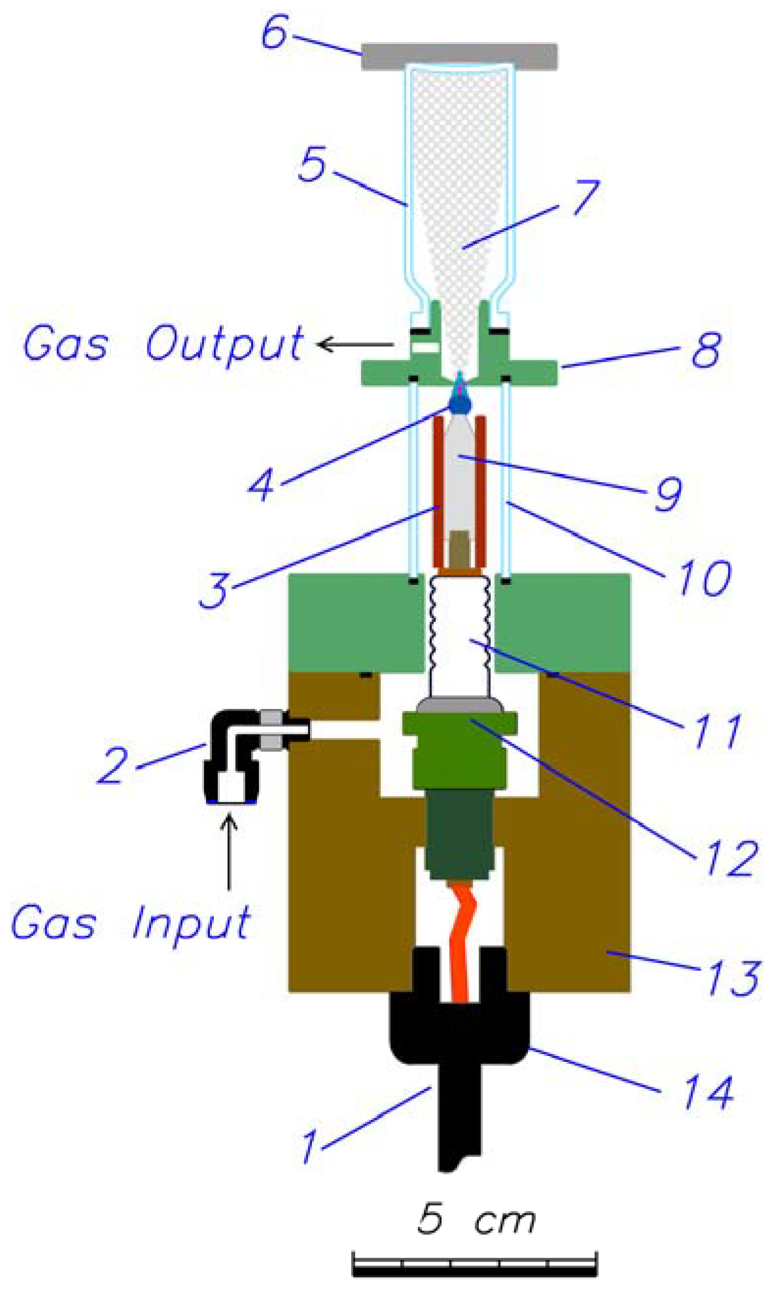
An illustration of the system which was used for the formation of metal-containing plasma in an atmospheric-pressure discharge is shown in
Figure 1. The discharge gap of the plasma source is formed by an aluminum (Al) anode and molybdenum (Mo) cathode. Most of the cathode has a cylindrical shape, which morphs into a truncated cone (the working surface) at the end facing the anode. The cathode diameter is 6.5 mm, and the angle at the apex of the truncated cone is 60°. This design feature follows from temperature conditions in the discharge under which stable operation occurs while maintaining the discharge gap geometry and cathode mechanical strength. The anode is in the form of a disk with a central aperture. The back of the anode serves as part of a 10 mL glass vial mounted to collect the erosion products from the cathode; this container can be replaced by another, as necessary. The discharge gap is located inside a quartz tube with an outer diameter of 20 mm and wall thickness of 1.2 mm, allowing not only visual observation of the discharge but also the recording of plasma emission spectra over a wide spectral range. The cathode is connected to the negative terminal of a power supply through a ceramic/metal current feedthrough. In the main body, made of Al alloy, this current feedthrough is fastened by a threaded connector.
In operation of the plasma source, the current feedthrough retains its mechanical strength and insulating properties at temperatures up to 1000 K. A hole with a centering nut is located at the bottom of the main body, providing connection to a cable to the negative terminal of the power supply. The main body is at anode potential and is connected to the positive terminal of the power supply. Gas (argon or helium) is admitted to the discharge gap through an inlet in the main body, and is removed from the discharge chamber through an outlet in the side of the anode. The gas flow rate during experiments was approximately 750 sccm, taking into account the fact that the working gas was heated to a temperature of about 100 degrees Celsius (approximately 373 K). All joints are sealed with heat-resistant graphite packing gaskets.
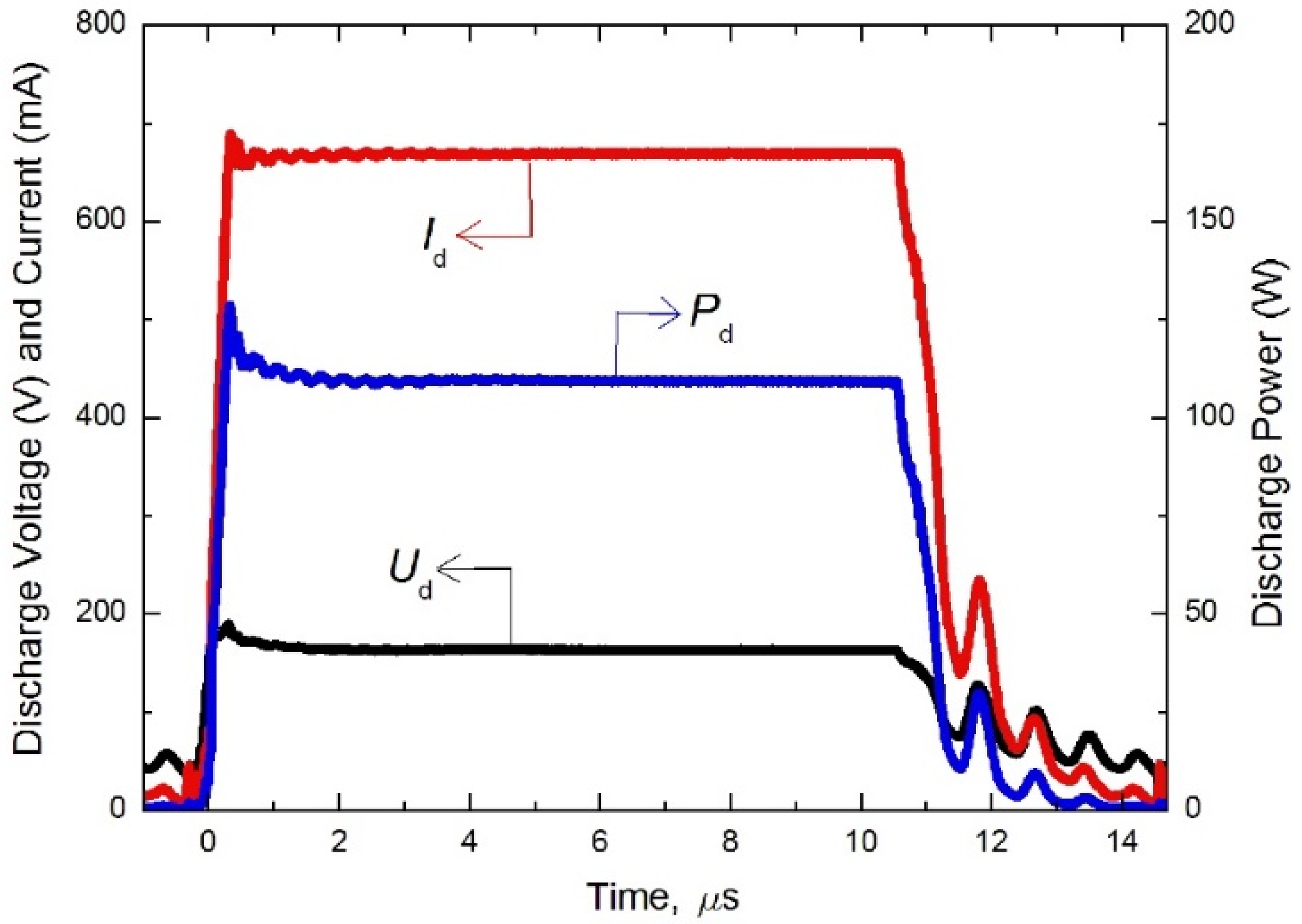
The power supply operates in a repetitively pulsed mode, generating negative polarity pulses which feed the gap. The positive terminal of the power supply is grounded. The temporal behavior of the discharge pulse in argon is shown in
Figure 2. During the pulse plateau (Δt = 2–10 μs), the discharge voltage U
d and discharge current I
d were 180 V and 670 mA, respectively. In helium, the discharge voltage was U
d = 250 V at the same I
d. Thus, the pulse power P
He ≈ 167 W in helium was greater than that in argon, P
Ar ≈ 120 W. The pulse repetition rate was 67 kHz, for a duty cycle of 0.78.
The source of In atoms was an indium cap covering the working surface of the molybdenum cathode. To form this cap, a ceramic tube was put on the cathode, and a piece of metallic indium (3 × 3 × 3 mm) placed on the top of the truncated cone (the cathode top). The indium melts in 5–6 min of discharge in argon. The molten indium wet the cathode surface and formed a ball-shaped cap; this shape was generated by the surface tension of the molten metal. According to the empirical expression presented in Ref. [
38], the surface tension of liquid indium at a characteristic value of the cathode–crucible temperature of 600 ± 30 degrees Celsius, measured by the contact method using a thermocouple, was approximately 518 mN/m (518 dynes/cm). The surface tension was 518 mN/m, which corresponded to a surface energy of 5.18 × 10
−5 J/cm
2. It is easy to estimate the energy density dissipated near the working surface of the cathode in one pulse of the discharge current. For example, when the discharge operated in an argon flow with a current of 670 mA, at a voltage of 180 V, and a pulse duration of 10 μs, with an active cathode surface area equal to the area of a hemisphere with a radius of 4 mm–0.25 cm
2, it was approximately 480 × 10
−5 J/cm
2. Thus, it can be concluded that sufficient energy was imparted to the surface of the meniscus formed by molten indium to overcome the surface tension.
The ceramic tube placed on the cathode, in turn, prevented the runoff of liquid indium. After some operation time, the power was turned off and the system allowed to cool, after which the tube was removed. In the experiments, the absence of this ceramic tube had no effect on discharge stability and the generation of a stream of In atoms.
The presence of In in the discharge was established by spectral analysis of the optical radiation emitted by the plasma. The optical measurement scheme was arranged as follows. A converging lens of focal length 75 mm was used to project an image of the discharge onto a screen through a 1 mm aperture. A lens connected to a fiber optic cable was positioned opposite the aperture on the reverse side of the screen, and close to it. The light guide, in turn, was mounted to the input of an HR4000CG-UV-NIR (OceanOptics Inc., Dunedin, FL, USA) spectrometer operating over the wavelength range Δλ = 200–1100 nm. The instrumental function of the spectrometer is Δλ
instr ~0.1 nm. In this way, the plasma optical radiation spectrum incident upon the aperture in the screen was recorded. For all elements of the optical measuring system, there are dependencies of the transmittance and sensitivity on the wavelength, provided either by the device or measured in-house using well-known methods and calibrated radiation sources. The identification of atomic In in the plasma was performed using the NIST database (National Institute of Standards and Technology, Gaithersburg, MD, USA) [
39].
The structural parameters (shape, size, and phase composition) of particles synthesized in the atmospheric-pressure plasma in rare (Ar or He) gas flow were explored using a JEM 2100 transmission electron microscope (Jeol, Tokyo, Japan) operating at an accelerating voltage of 200 kV. The elemental composition of the particles was determined using an “INCA Energy” energy-dispersive spectrometer (Oxford Instruments, Abingdon, UK) mounted on a transmission electron microscope. The procedure was carried out by accumulating maps of the distribution of elements, as well as spectra from individual particles (point analysis). After the cooling and condensation of the erosion products of indium, powder layers were obtained. These layers were subsequently dispersed by sonication in a solution of ethyl alcohol and then deposited on carbon-coated copper grids. X-ray diffraction studies of all samples were carried out using a Shimadzu XRD-7000 (Shimadzu, Kyoto, Japan) diffractometer in Cu-K
α radiation. The lattice parameter of the cubic phase was determined by a precision method with the construction of extrapolation dependencies a
cubic on the {2-1[(cos2θ/sinθ) + (cos2θ/θ)]} function. The lattice parameter measurement accuracy was Δa = ±0.00005 nm. Samples for X-ray diffraction studies were made on sheet copper. During the coating process, the samples were placed with the polished side directly towards the aperture in the anode. In this case, the glass vial at the top of the setup (see
Figure 1) was removed. When analyzing the diffraction patterns, data on the structure of possible crystalline phases corresponding to the In-O system, taken from the database of powder X-ray diffraction patterns PDF-2, were used [
40].
3. Results
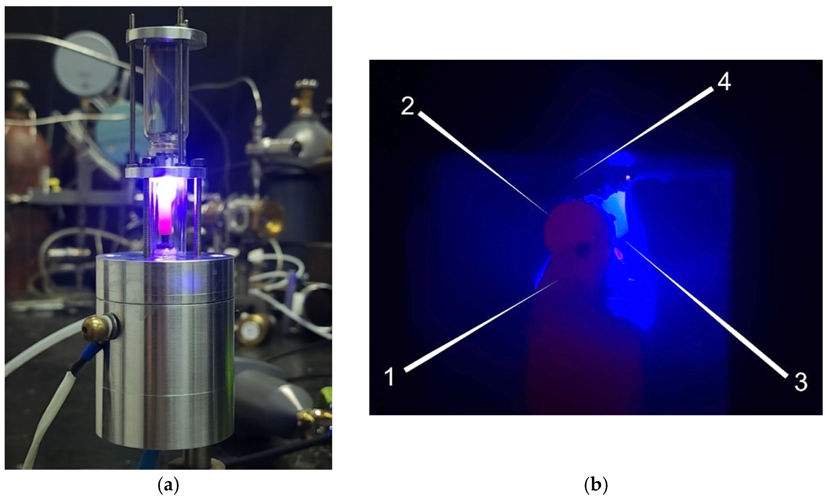
A photographic image of the metal-containing plasma source in operation is shown in
Figure 3a.
Figure 3b shows an image of the discharge gap, in argon, captured on an enlarged scale and with reduced brightness.
Figure 3b shows clearly a meniscus of liquid indium (2) surrounded by cathode glow, the discharge column (3), and a “fringe” (4) formed by thermal erosion products of indium condensed near the anode aperture. The flow of working gas (Ar or He) through the anode hole transports the main part of the flow of indium particles from the discharge zone into the glass vial volume, where they settle on the wall inner surface.
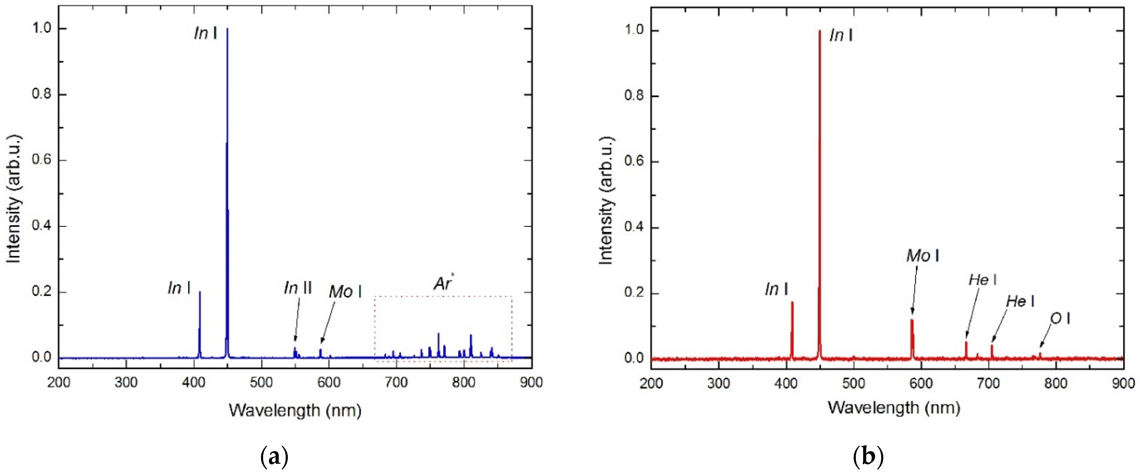
The presence of In particles was identified by the emission spectra of the plasma (
Figure 4). Thus, along with Ar or He atomic lines, lines of atomic indium with λ
In1 = 410.17 nm and λ
In2 = 451.1 nm were observed in the survey spectra. Note that the emission spectra contain the line of excited atomic molybdenum Mo I (λ
Mo = 587.39 nm), indicating the erosion of the top part of the cathode.
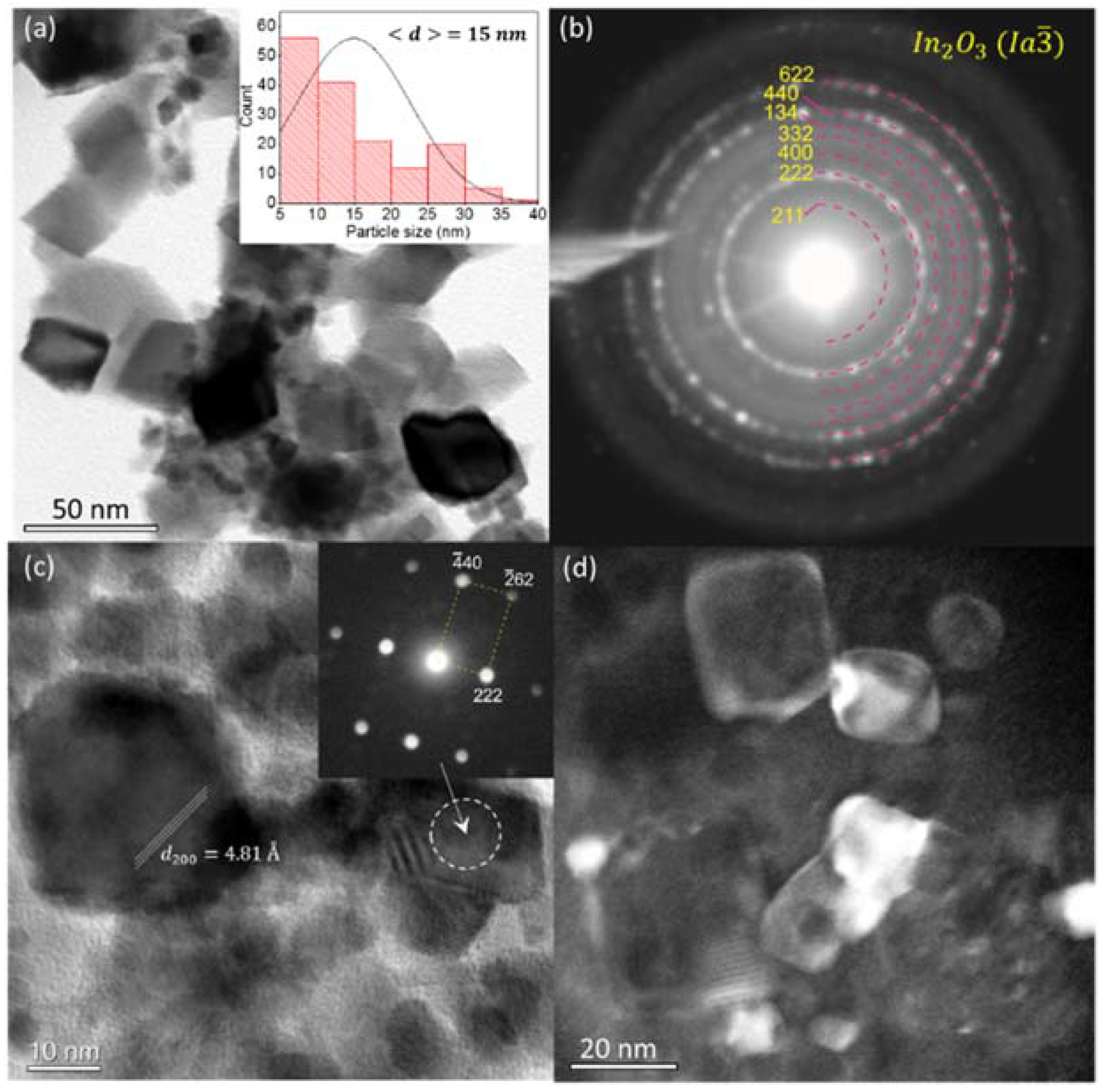
The results of electron microscope studies of the structure of the erosion products of the material of the ball-shaped cathode tip formed by molten In are shown in
Figure 5,
Figure 6 and
Figure 7. TEM images of the particles condensed in the vicinity of the In cathode cap at the end of a ceramic tube placed on the Mo cathode are shown in
Figure 5. Thus, the bright-field image (
Figure 5a) demonstrates the presence of particles with a square cross-section. Nanodispersed particles of spherical or round shape were observed less often. The interpretation of the ring microdiffraction results (
Figure 5b) shows the presence of a single phase of indium oxide with a cubic lattice, which is described by the Pearson symbol
cI80 and the symmetry group
Ia¯3. The distribution and thickness of the quasi-ring reflections indicate the nanocrystalline structure of the particles of synthesized powder. The high-resolution image (
Figure 5c) contains moiré patterns resulting from the superposition of misoriented In
2O
3 lattices. In this case, the interplanar distances in this phase, measured by the diameter of the rings on microdiffraction and high-resolution patterns, differ from reference distances (pdf card #03-065-3170) [
40]. This may indicate a defective structure of indium oxide crystals and their nonstoichiometric composition. The first assumption is supported by the deformation contrast observed on large particles and arising on single dislocations. A typical nanodiffraction pattern from an individual particle is shown in the inset to
Figure 5c and represents the reciprocal lattice of the In
2O
3 phase of the same crystal structure described above. The average particle size measured from a series of dark-field images (
Figure 5d) is 15 ± 8 nm. The corresponding particle size distribution histogram is shown in the inset to
Figure 5a.
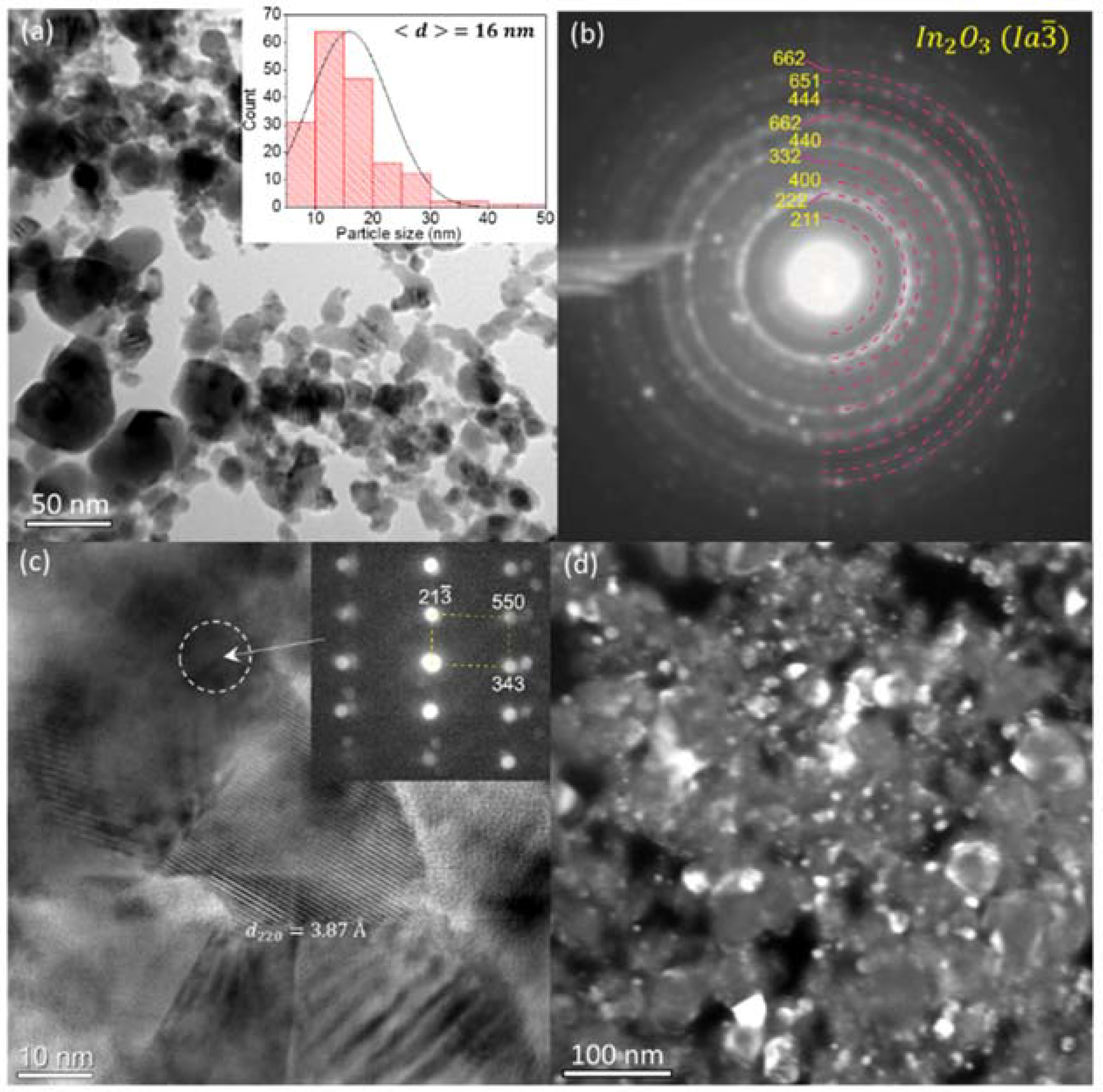
Analysis of TEM images of particles synthesized in argon plasma and condensed on the inner surfaces of the walls of the discharge chamber quartz tube and the glass vial located behind the anode indicated a greater variety of morphological types of crystallites, which had both straight faces and equiaxed shapes. The particles were grouped into conglomerates up to 100 nm in dimensions and belonged to the bcc phase of In
2O
3. This was confirmed by the interpretation of the corresponding micro- (
Figure 6b) and nanodiffraction patterns (inset to
Figure 6c). Planar stacking faults were contained in the particle structure (
Figure 6c). The nature of these defects can be associated with the formation of dislocations during crystal growth. The average particle size (≈16 ± 7 nm) in this case remained practically unchanged. The dark-field image (
Figure 6d) shows an inhomogeneous diffraction contrast that intensifies near the boundaries of conjugated particles.
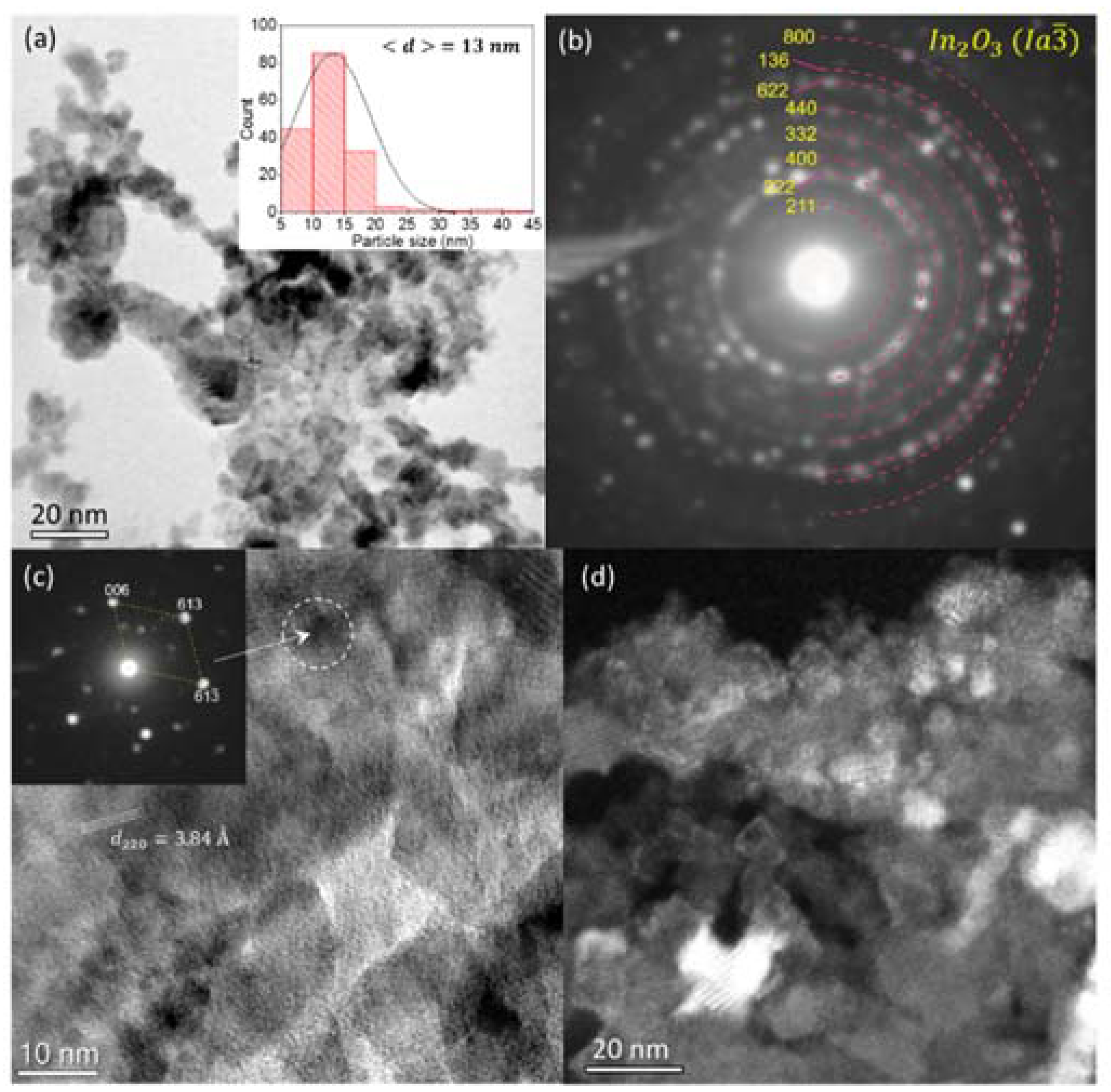
Indium erosion products condensed in a helium medium in the form of a powder collected on the glass vial walls contained In
2O
3 particles, predominantly of irregular shape. The boundaries of some crystallites were blurred and did not contain flat faces typical for recrystallized grains (
Figure 7a). Microdiffraction (
Figure 7b) from the largest clusters of particles had a quasi-ring character and consisted of a smaller number of point reflections. This, in turn, was associated with the formation of relatively large particles up to 50 nm in size. The identification of ring reflections demonstrated the same set of interplanar distances of the In
2O
3 phase as in the previous cases (
Figure 5b and
Figure 6b). The average particle size of the powder was reduced to 13 ± 6 nm. In high-resolution images (
Figure 7c,d), the contrast from dislocations and the interference contrast from moiré fringes were observed.
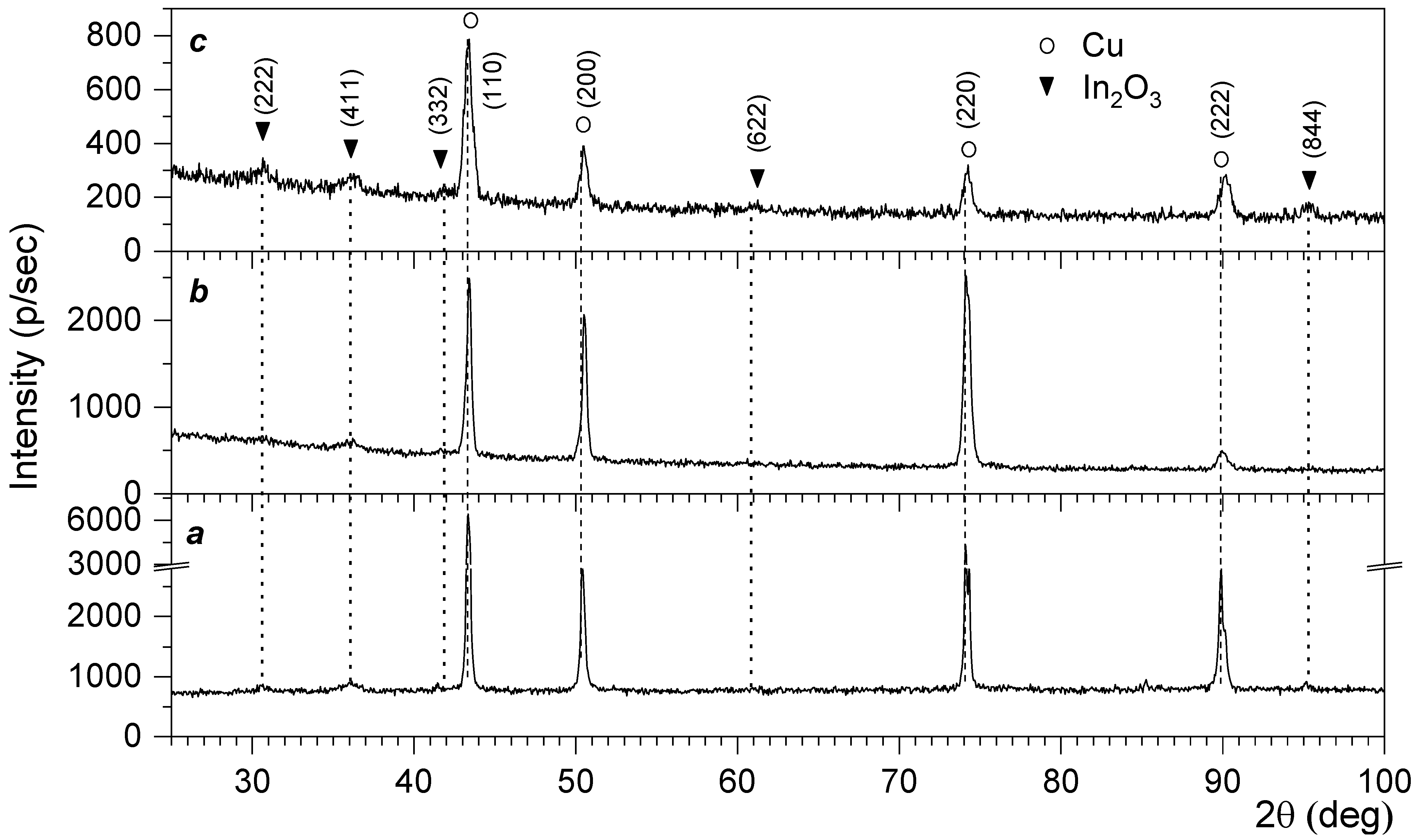
X-ray diffraction analysis of coatings based on indium erosion products during the discharge in an argon flow deposited on copper substrates (2 × 2 cm
2) showed (see
Figure 8) that the diffraction pattern contained only reflections from two phases: Cu (Fm-3m (225), 00-001-1241) and In
2O
3 (Ia-3 (206), 03-065-3170). These phases have a cubic structure [
40]. To separate the contributions to the diffraction patterns from the coating and the copper substrate, asymmetric survey schemes were carried out at grazing angles α
1 = 12° (
Figure 8b) and α
2 = 5° (
Figure 8c). These studies show that with the decrease in the grazing angle α, which is equivalent to the decrease in the thickness of the analyzed layer, the intensity of reflections of the In
2O
3 phase on the diffractograms increases (
Figure 8c). Accordingly, the layer containing the phase of indium oxide (III) was on the surface. The lattice parameter of the Cu-based cubic phase was
a = 0.3618 nm, and for the In
2O
3 phase
a = 1.013 nm.
The results of energy-dispersive analysis of powder particles, performed by means of transmission electron microscopy equipped with an appropriate spectrometer (
Table 1), indicate a deviation in the chemical composition from stoichiometric. The proportion of indium in relation to oxygen was 1:4. In this case, an impurity of Mo (in trace concentration) was detected in the particles.
4. Discussion
The appearance of the visually observable jet flowing through the anode hole from the region of atmospheric-pressure plasma is a consequence of the fact that, because of processes at the cathode, flows of metal atoms are generated due to thermal erosion of the molten material of the cathode cap. A possible mechanism for this phenomenon could be based on the transport of metal atoms by the working gas (Ar or He) flow from the thinnest vapor layer above the surface of the liquid metal meniscus formed at the top of the cathode. Direct evaporation in this case is difficult, since the temperature of the cathode, under these conditions, is significantly lower than the boiling point of indium. Thermal diffusion across the meniscus surface is the reason why atoms enter the discharge gap, where they are then ionized and excited in collisions with plasma electrons.
Analysis of the emission spectra shows that strong In atomic lines are observed in addition to lines of atoms of the working gas—argon or helium. Note that in the wavelength range under consideration, atomic transitions of metal atoms account for the radiation energy, which makes up a significant share of the spectral energy distribution over the entire range. It follows from the observed spectra that the molybdenum cathode also contributes to the plasma emission. This is confirmed by the fact that when visualizing the near-cathode region (see
Figure 3b), it is clearly seen that the cathode glow covers not only the indium meniscus, but also the molybdenum body of the cathode that is not wetted with indium. Since the temperature of the cathode is much lower than the melting temperature of Mo, the proposed mechanism of Mo atomic diffusion into the vapor layer and subsequent transport upon interaction with the working gas flow, most likely cannot be implemented. In this regard, it should be assumed that electrical erosion can occur in the cathode spots of a sub-microsecond spark discharge that occurs at the initiation of individual discharge pulses. In any case, this phenomenon deserves special attention and requires a more detailed study.
Structural studies of the dispersed individual nanosized powder particles per-formed using transmission electron microscopy and powder aggregation in the form of a coating using X-ray diffractometry show that the data obtained by these independent methods are in good agreement. It was found that the structure of powder particles corresponded to a single phase of indium oxide (III) with a body-centered cubic (bcc) lattice with a lattice parameter a = 1.013 nm. Energy-dispersive analysis shows that, within the framework of this work, these particles are represented by non-stoichiometric indium oxide In2O3 with a nanocrystalline structure (<d> = 13–16 nm), regardless of the working gas (Ar or He).
Note that among the investigated erosion products of the indium cathode tip, particles of metallic indium were completely absent. When coatings are deposited on copper substrates placed in ambient air, this is an obvious consequence. The metal-containing plasma jet is mixed with ambient air at the source outlet, where the transported indium particles are oxidized. However, the use of a container for collecting the erosion products, in the form of a glass vial placed immediately after the anode hole and hermetically fixed to the anode through a sealing gasket, assumes that both the generation of metal particles during discharge operation and their collection are carried out in an airless environment. The design of the plasma source allows continuous pumping of the working rare gas, both during dispersion of In in the discharge plasma and after it is turned off, up to the cooling of the structural elements of the source. However, in this case also, only In2O3 particles are seen in the composition of the erosion products. This experimental fact can be associated with the oxidation of metallic indium particles as a result of interaction with oxygen already in the discharge plasma, since the working gases are not 100% pure and contain small quantities of nitrogen, oxygen, and water vapor admixtures; the volume fraction of oxygen in these mixtures is about 2 × 10⁻⁴%. One should also not exclude the possibility of the formation of indium oxide as a result of interaction with oxygen of metal particles located on the walls of the glass vial, as well as on the anode and other elements of the plasma source discharge system after its operation is completed, as a result of prolonged exposure to the ambient atmosphere. The production of metallic indium nanoparticles was not the aim of this study. Nevertheless, plasma-chemical processes involving dispersed metal particles with a gaseous medium are of considerable interest and call for a more detailed study.

 ,
, 


