
Photovoltaic Solar Cells: A Review


1
Department of Mechanical Engineering, Universiti Tenaga Nasional, Kajang 43000, Selangor, Malaysia
2
Institute of Power Engineering, Universiti Tenaga Nasional, Kajang 43000, Selangor, Malaysia
*
Authors to whom correspondence should be addressed.
Appl. Syst. Innov. 2022, 5(4), 67; https://doi.org/10.3390/asi5040067
Submission received: 7 October 2021
/
Revised: 3 November 2021
/
Accepted: 10 November 2021
/
Published: 8 July 2022
Abstract
:Employing sunlight to produce electrical energy has been demonstrated to be one of the most promising solutions to the world’s energy crisis. The device to convert solar energy to electrical energy, a solar cell, must be reliable and cost-effective to compete with traditional resources. This paper reviews many basics of photovoltaic (PV) cells, such as the working principle of the PV cell, main physical properties of PV cell materials, the significance of gallium arsenide (GaAs) thin films in solar technology, their prospects, and some mathematical analysis of p-n junction solar cells. Furthermore, the paper presents the standard model of solar cells with the application of this model to different PV technologies together with the main findings. Moreover, the paper explores the role of numerical and mathematical modelling of PV cells by MATLAB/Simulink and COMSOL in evaluating the power conversion efficiency (PCE) of the PV cells and determining the main parameters affecting the power output at various conditions.
1. Introduction
Global environmental concerns and the increasing energy demand, coupled with continuous progress in renewable energy technology, are encouraging the utilization of alternative energy resources. Solar energy is the most affordable and abundant of all long-term natural resources to date [1]. Solar PV technology is one of the optimum ways to utilize solar power to generate electricity by converting the sunlight to direct current in solar cells or PV cells [2,3].
PV energy conversion utilizes devices based on electronic semiconductors, particularly but not exclusively, crystalline silicon (c-Si) or thin-film semiconductor materials. A (c-Si) based solar system is usually constructed from two essential types of crystalline materials, monocrystalline and multi-crystalline solar modules. Single-crystal semiconductors have superior electrical characteristics (20% efficiency) comparable to polycrystalline materials. Nevertheless, monocrystalline PV modules are non-economical as crystalline wafer-based technology is too expensive [4,5].
Thin film technology is an alternative technique that uses usually amorphous silicon (a-Si) or other semiconductor materials (i.e., cadmium telluride (CdTe), copper indium gallium selenide (CIGS), or gallium arsenide (GaAs)) in its structure. A thin-film solar cell is much thinner than a conventional (c-Si) cell. The film’s thickness is a few nanometers (nm) to tens of micrometres (μm), which allows thin-film modules to be light and flexible. Furthermore, thin-film technology is generally cost-effective as compared to (c-Si) wafer-based technology [6,7].
The (a-Si) solar cell is one of the most common thin-film technologies with cell efficiency (5–7%). The efficiency increases with double and triple junction design to 8–10%. (a-Si) thin-film offers lower efficiency when compared to the (c-Si) module. In addition, (a-Si) thin film is prone to degradation due to the reaction of (a-Si) with the environment, such as with the air or water vapour [8,9].
Furthermore, CdTe thin film nearly competes with the (c-Si) cell in cost/watt. Nevertheless, tellurium supplies are restricted and cadmium is highly poisonous [10].
Moreover, CIGS PV cell is another film technology with an acceptable cell efficiency of (~20%). However, the cost of fabrication CIGS solar cell is higher than CdTe- based thin film and (c-Si) wafer [11].
Moreover, GaAs thin film is a crystalline compound form of (Ga) and (As). It has a high resistivity to heat and radiation, which affect the efficiency of solar cells. Although a GaAs solar module is expensive, it holds the world’s record in efficiency (over 30%). Since the industry favours efficiency over cost for outer space power generation, multijunction GaAs cells are usually used for concentrator solar structures and spacecraft-based solar energy as they can be operated at an extremely higher temperatures compared to a (c-Si) based solar system [12,13,14].
This paper reviews some basic solar cells physics, materials employed in PV cells, the importance of GaAs thin films in solar technology, their future trends, and challenges in solar cells. Furthermore, the paper presents the standard model of solar cells with the application of this model to different PV technologies together with the main results. Besides, the paper explores the role of mathematical and numerical modelling of PV cells in MATLAB/Simulink and COMSOL Multiphysics in investigating the (I-V) and (P-V) characteristics and enhancing the PCE of PV cells.
2. Solar Cells
2.1. The Working Principle of PV Cells
A PV cell is the essential unit of a solar energy generation system in which sunlight is promptly converted to electrical energy. The solar cell is a p-n junction device. n-type refers to the negatively charged electrons donated by donor impurity atoms and p-type refers to the positively charged holes created by acceptor impurity atoms, referring to Figure 1 of a PV structure [15,16,17].
The working principle of solar cells is based on the photovoltaic effect. The PV effect can be divided into three essential procedures [18,19,20].
- Absorption of photons in a p-n junction electronic semiconductor to generate the charge carriers (electron-hole pairs). The absorption of a photon with energy (E = hυ) higher than the gap energy ‘Eg’ of the doped semiconductor material means that its energy is used to excite an electron from the valence band ‘Eυ’ to the conduction band ‘Ec’ leaving a void (hole) at the valance level. Additional kinetic energy is given to the electron or hole by the excess photon energy (hυ–hυ0). ‘hυ0′ is the minimum energy or work function of the semiconductor required to generate an electron-hole pair. The work function here represents the energy gap. The excess energy is dissipated as heat in the semiconductor [21,22].
- Consequent separation of the light-generated charge carriers. In an external solar circuit, the holes can flow away from the junction through the p-region, and electrons can flow out across the n-region and pass through the circuit before they recombine with the holes.
- Finally, the separated electrons can be used to drive an electric circuit. After the electrons passed through the circuit, they will recombine with the holes.
The n-type must be designed thinner than the p-type. Thus, the electrons can pass through the circuit in a short time and generate current before they recombine with the holes. Besides, an anti-reflective coating is applied over the n-layer to reduce surface reflection and enhance the transmission of the light to the semiconductor material.
All the aspects presented in this section will be discussed in more detail in the next sections.
2.2. Solar Cell Panels
Solar panels are multiple solar cells connected in series and parallel to produce a certain power output. One PV cell is unfeasible for most applications as it can only produce about 0.5 V. For example, six cells are connected in series, the cell is assumed to have the same current as a single cell and ideal 3 V (6 × 0.5 V). Series cells are also connected in parallel for higher current capacity. If the six cells can generate 2 A, the series-parallel structure of twelve cells is supposed to generate 4 A and 3 V [23].
2.3. Components of Solar Power System
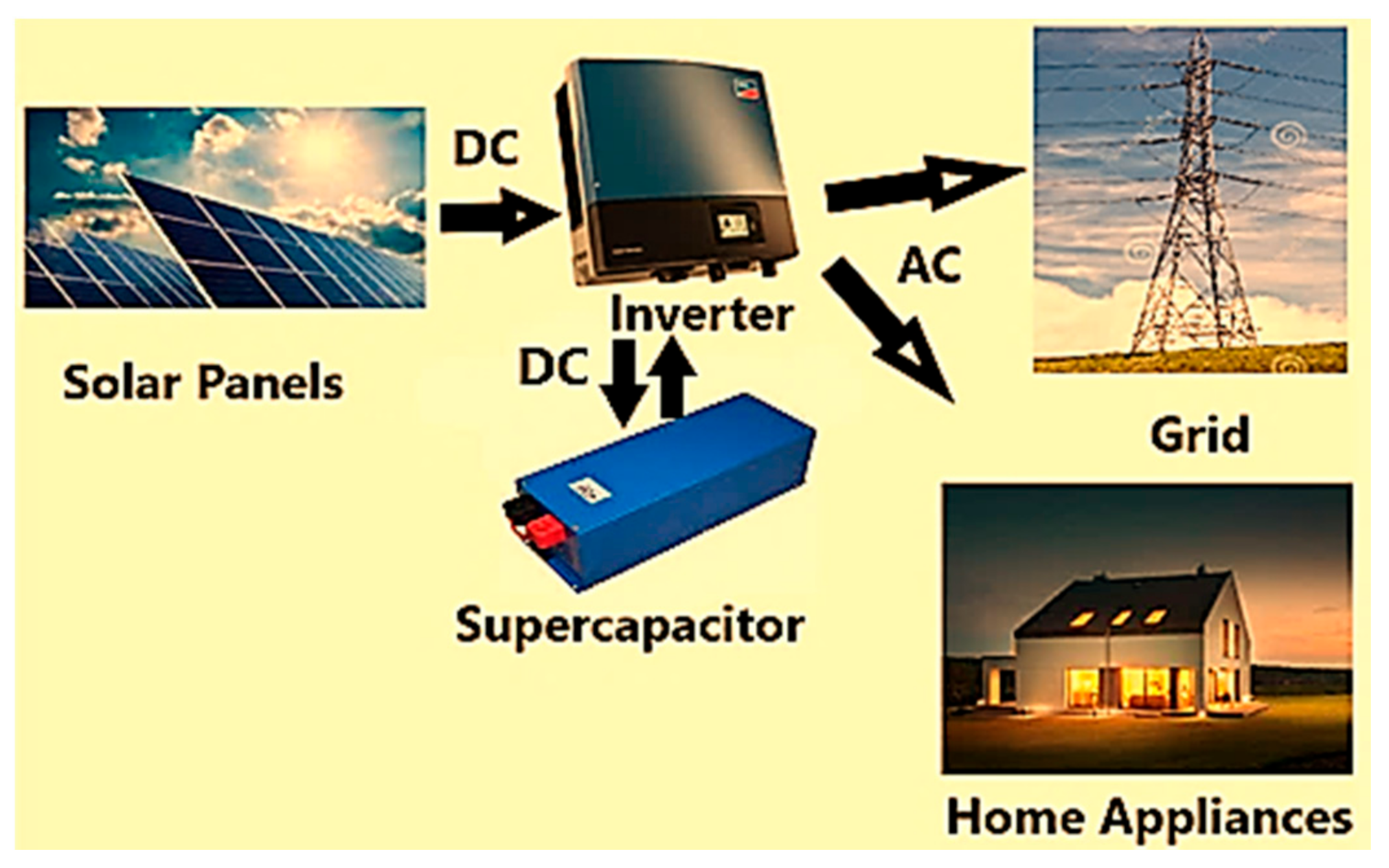
A PV system is composed of a solar panel, supercapacitor, and inverter. The solar panel absorbs photon energy and transforms it into electricity through the PV mechanism. The supercapacitor backup is used to deliver additional energy only on sunny days. The generated DC power is transformed into AC loads to be appropriate for domestic use [23,24], as shown in Figure 2.
2.4. p-n Junction Solar Cell
2.4.1. Formation of the Depletion Region
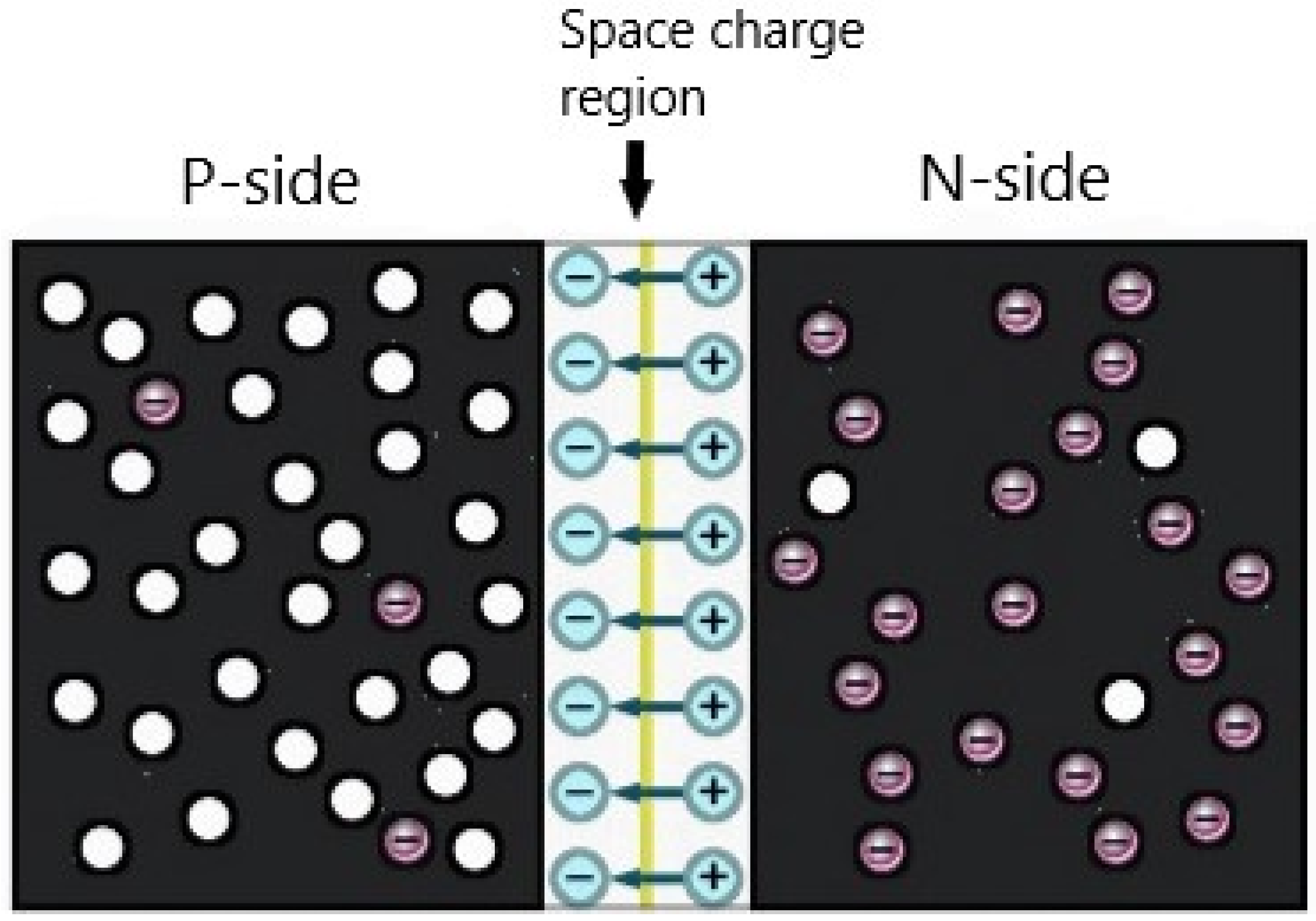
A solar cell in a basic term is a semiconductor diode that has been carefully designed to generate power from the sunlight. A diode is a single crystal semiconductor material such as silicon, having one side doped with pentavalent impurities forming n-type and another side doped with trivalent impurities as p-type. The doping process creates additional mobile carriers called majority carriers in each respective region. When n-region and p-region semiconductors are brought into contact, electrons of the n-section will diffuse into the p-section leaving a region of positively charged donor atoms in the p-n interface near the n-zone. Likewise, a net of negatively charged acceptor atoms is left behind in the p-n junction near the p-zone as holes diffuse from p-region to n-region. The consequent jumps of the valence electrons can be noted as a motion of the holes. The diffusion of electrons and holes will create a current called diffusion current ‘Idiff’ and a depleted area of charge carriers, referred to as the depletion region or space charge region. All electrons and holes are swept out of the depletion region by a generated electric field, which prevents any additional flow of the charge carriers [25], as shown Figure 3 below.
The net flow of electrons and holes in a semiconductor under equilibrium conditions will generate currents, namely diffusion current ‘Idiff’ as a result of the concentration difference and drift current ‘Idrift’ as a result of the generated field at the junction [26]. The diffusion current of electrons ‘In-diff’ is expressed by:
Likewise, the typical diffusion current density of holes is given by:
where dn/dx and dp/dx are the ratios of the change in particles’ density to the change in the diffusion distance of electrons and holes, respectively. Due to a built-in electric field, ‘Idrift’ is generated, which is opposite to the ‘Idiff’ [27].
The drift current due to drift of electrons ‘In-drift’ is given by:
where ‘µn’ is the electron’s mobility, ‘E’ is the electric field in the depletion region, and ‘υdn’ is the drift velocity of electrons.
Similarly, ‘Ip-drift’ due to drift of holes is expressed as:
‘µp’ is the holes mobility and ‘υdp’ is the average drift velocity of holes.
The net ‘Idrift’ due to drift of holes and electrons is as follows:
The above equation can be written as:
‘σ’ given by (Ω/cm) is the conductivity of the electronic semiconductor. For nondegenerate semiconductors, there are no net currents in the depletion region as ‘Idrift’ and ‘Idiff’ are balanced at the state of equilibrium. This leads to the Einstein relation:
The particle mobility ‘µ’ gives a sign of how well an electron or a hole moves in a semiconductor due to an electric field while the particle diffusion coefficient ‘D’ indicates how well the particles move in the semiconductor owing to the concentration gradient [28].
2.4.2. p-n Junction Solar Cell under Applied Voltage
If the diode is connected to a forward bias external voltage, the depletion region will shrink. The negative charge carriers (electrons) and positive charge carriers (holes) are repelled from the negative and positive terminal respectively toward the p-n junction. Consequently, the energy required for the charge carriers to flow across the depletion region is lowered, referring to Figure 4.
Once the applied voltage reaches the barrier potential, electrons start to flow through the space charge region. The diode current in the forward bias mode is expressed by the ideal Shockley equation. The current through the diode exponentially increases with increasing forward bias external voltage [29].
where ‘Id’ is the diode current as the mobile carriers move through the junction; ‘I0′ is the saturation diode current in the depletion area at room temperature ‘T’, 300 K; ‘V’ is the external voltage; k: Boltzmann’s constant, 1.3805 × 10⁻²³ J/K, and ‘e’ is the electron charge, 1.60217657 × 10⁻¹⁹ coulombs [30].
2.4.3. PV Cell under Illumination
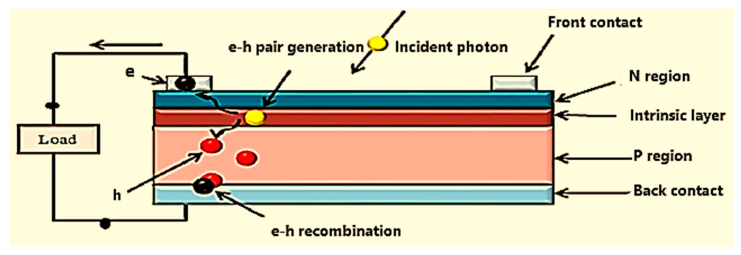
When the incident light is absorbed in the electronic semiconductor forming a p-n junction, it generates pairs of negative and positive mobile charges (e− and h+). The electrons move out of the n-area to the metal contacts across the negative contact then through the load. Next, the electrons move back into the positive contact and finally to the p-area where they can recombine with holes, as shown in Figure 5.
As mentioned earlier, the behaviour of the p-n junction diode is employed in solar cells. Therefore, the basic qualitative discussion and mathematical analysis used for diodes are also be applied to the p-n junction PV cell. Without illumination, a PV cell has the same electrical characteristics of a large diode. Under illumination, the output current is simply a summation of the current under the dark condition ‘Id’ and photocurrent ‘Iph’ [25], which is expressed as:
To summarize the generated currents:
- The net flow of the electrons and holes in a p-n junction semiconductor under equilibrium conditions will generate two currents: ‘Idiff’ and ‘Idrift’. These currents balance and cancel each other at the equilibrium state.
- If an external source is deployed to the p-n junction, the generated current is the diode current ‘Id’.
- Under illumination, the p-n junction will present another current called light or photocurrent ‘Iph’.
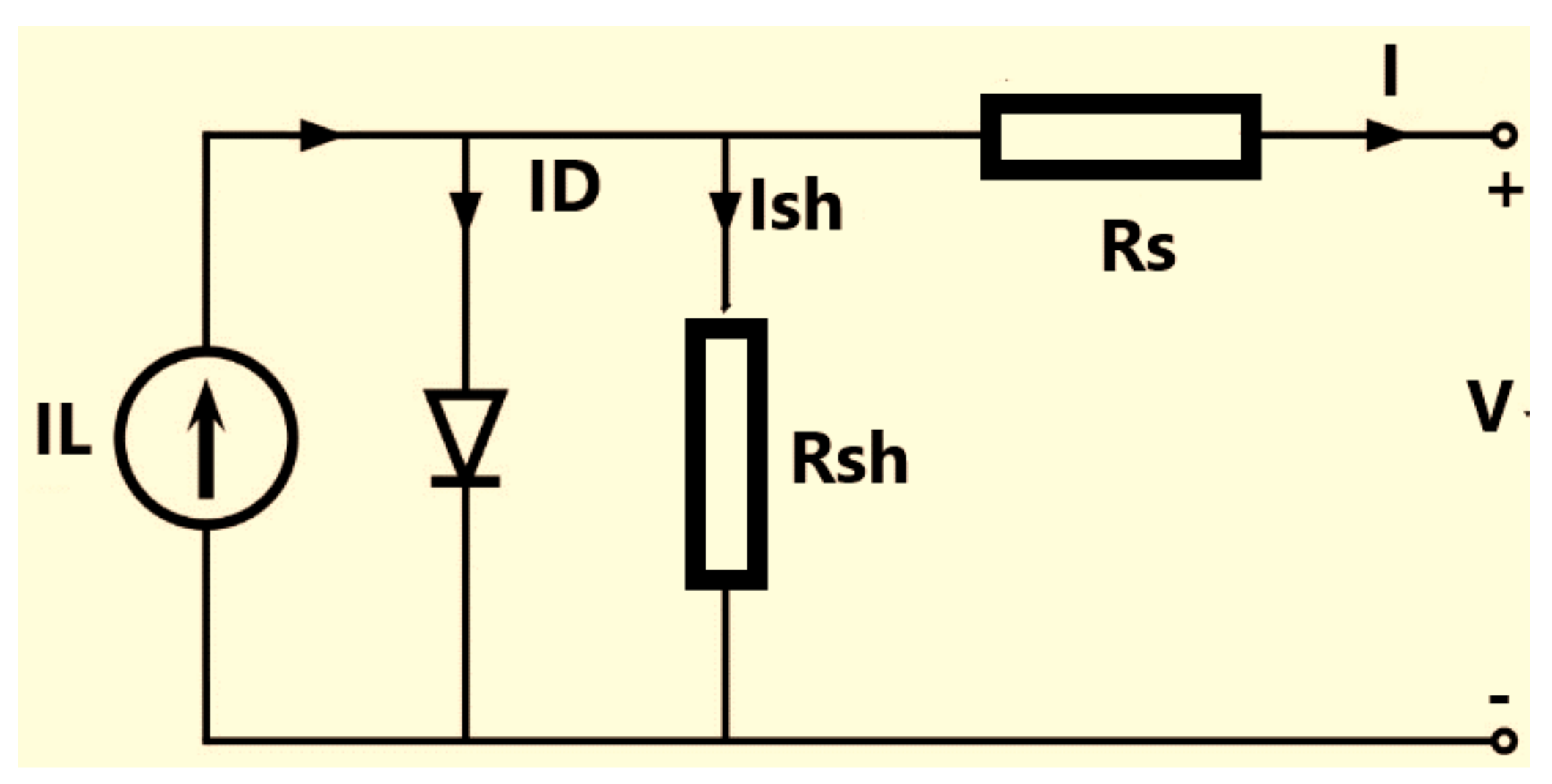
The equivalent circuit of the solar cell is presented below. In real cells, power is dissipated through a series resistance ‘Rs’ created due to the ohmic contact in the front surface and shunt resistance ‘Rsh’ due to leakage current. Therefore, for a practical solar cell, the equivalent circuit includes ‘Rsh’ added in parallel with the diode and ‘Rs’ added in series with the load as given below, Figure 6 [31,32,33].
Therefore, the above equation can be written as follows:
2.5. I-V and P-V Characteristics
Figure 7 clarifies the (I-V) and (P-V) curves of PV cells.
The PV cell should be managed to give a maximum power output ‘Pmax’ at a maximum voltage ‘VM’ and maximum current ‘IM’ [34].
The external parameters defined by the I-V curve are as follows:
- Short-circuit current density ‘Isc’ occurs at (R = 0 and V = 0)
- Open-circuit voltage ‘Voc’ (no-load, I = 0 and R = ∞)
- Fill factor ‘FF’ that represents the ratio of ‘Pmax’ to the electrical output of ‘Voc’ and ‘Isc’
2.6. Design Considerations
The design of a PV cell is defined by the cell structure [37]. Solar cells can be fabricated in different designs. First, a single-junction solar cell, which consists of a highly doped emitter layer and a lightly doped base layer. For a single-junction PV cell, GaAs is best suited to achieve the highest efficiency, nearly 30%, due to its bandgap (1.42 eV) being near to the ideal bandgap and high absorption coefficient, which offers substantial benefit in the design and fabrication of highly efficient PV devices [38,39]. Highly efficient n-on-p single-junction GaAs thin-film solar cells have been fabricated by [40]. A metal combination of AuBe/Pt/Au was employed as a new p-type ohmic contact. The PCE of the fabricated single-junction GaAs thin-film solar cells reached 22.08% under Air Mass (AM) 1.5 global illumination. Another experiment by [41] demonstrated a PV GaAs device based on single junction thin film under the non-concentrated light (1 sun illumination), achieving a high efficiency of 27.6%.
Second, multijunction PV cells are the most effective solar cells to date. GaAs-based multijunction PV cells achieved the highest efficiency of 42.3%, as it is possible to grow three or more junctions for one cell. The novel designs of Si and GaAs wafer-based double-heterojunction solar cells were demonstrated by [42,43]. The cells were comprised of five layers, a cathode metal layer, three layers of semiconductor materials of III–V, II–VI, and IV families, and a layer of anode metal. The device structures have been optimized for the analysis of the PCE of the Si and GaAs solar cells considering high defect densities at and near each heterojunction. The PCEs obtained were almost 38.9%.
Furthermore, p-i-n structures are developed by inserting an undoped or intrinsic layer (i) between very highly doped (p) and (n) regions. p-i-n structures increase the carrier’s lifespan and density in the undoped region. The intermediate layer has a very low concentration of usually n-type in the order of 1013 cm−3. The p-i-n structure offers carriers confinement in the intermediate undoped layer, providing a higher output current. In the forward bias, both types of carriers are injected into the intrinsic layer, leading to an increase in the carriers’ density and consequently the output current. The direct and flexible bandgap of the p-i-n double heterostructures offers a unique opportunity to develop highly efficient solar cells [44,45,46]. An experimental work by [47] focused on developing a p-i-n PV model with the compound materials AlGaInP/AlGaAs. The cell recorded the highest conversion efficiency of 51.50% under the AM 1.5 standard.
The performance of solar cells is affected by design considerations as well as the properties of the employed materials. Designers can select a small subset of the most promising materials to be employed for solar cells using, e.g., CES EduPack software [48]. Furthermore, doping and alloying affect the properties of the employed materials. For example, the density of donor atoms ‘Nd’ and acceptor atoms ‘Na’ affects the width of the depletion region. Moreover, adding some elements by alloying affects the physical properties of the employed materials [49].
2.7. Materials Employed in PV Cells
A concise comparison between the different materials used in PV cells nowadays with their advantages and drawbacks is presented in Table 1.
2.7.1. III-V PV Gallium Arsenide
GaAs (III-V binary semiconductor), a widely used electronic semiconductor in solar cells, is a crystalline PV material based on an element with three valence electrons, gallium (Ga), and an element with five valence electrons, arsenic (As). Therefore, the average valency is four electrons per atom. GaAs has a zinc blend crystal structure that consists of four (As) neighbouring atoms with every (Ga) atom and four neighbours (Ga) with every (As) atom, referring to the Figure 8. It has a direct bandgap equal to 1.42 eV at room temperature (300 K) where the lowest conduction band is vertically aligned with the highest valence band [60]. Thus, no transfer of momentum is required to excite an electron from the valence to the conduction band [71]. GaAs has a high resistivity to heat and radiation that affect the module performance compared to (c-Si) solar cells. Double heterojunction GaAs solar cells achieved the highest energy conversion efficiency by [42,72]. Many studies on single-junction GaAs cells achieved 28.8% power efficiency [54]. The highest efficiency of GaAs semiconductors was accomplished with a triple-junction, reaching up to 42.3%. However, the GaAs solar module is too expensive as gallium resources are limited [73]. Therefore, further improvement of higher efficiency and low-cost GaAs solar cells is significant in the PV solar system [74].
2.7.2. Future Trends
GaAs solar cells have contributed as concentrators and space solar cells [54] and are anticipated to create new markets, such as large-scale electric power systems and PV cell-powered electric vehicles. Single-junction GaAs solar cells, which are important as sub-cells for multijunction PV cells, have shown the highest ever stated efficiency (29.1%) under the standard AM 1.5 spectra for single-junction PV cells. GaAs multijunction solar cells of three junctions or more have been developed due to the limiting efficiency of single-junction PV cells. GaAs multijunction solar cells will be widely used in space because of their high obtained PCE. The concentrator PV (CPV) systems with several times more annual power generation capability than typical crystalline Si flat-plate systems will open a new market for charging stations including battery-powered electric vehicle applications. Multi-junction solar cells are greatly expected to be high-efficiency PV cells applied to solar cell-powered electric vehicles and large-scale PV power plants. Further development of super-high-efficiency and low-cost PV cells is crucial to create new markets [75,76].
2.8. Challenges in Solar Cells
Solar energy is the most promising clean energy resource that can directly be converted to electricity. It can almost provide stable power at a practical operating cost. Over the last few years, solar energy experienced fast growth as the clean energy demand is continuously increasing [77,78]. However, the efficiency of solar cells is still under research and development as it depends highly on the surrounding conditions [79] and fundamental properties of the solar module. The output power of solar cells is affected by many input factors, such as the shading effects, employed PV materials, temperature, the intensity of radiation received, parasitic resistances, weather conditions, solar cell design (e.g., p-i-n or double heterojunction), doping level, material properties and quality, etc. These parameters must be optimized to improve the obtained power efficiency [80]. For example, the most popular issue in PV cells is the drastic loss in power due to soiling on solar modules in desert regions. The dust blocks the sun in deserts and significantly affects the attractive energy of solar panels obtained in such areas [81,82]. The location of installation is another challenge since four seasons tend to have differences in the radiation and temperature that affect the power efficiency [83]. Some challenges also arise from the solar module itself. Mounting the solar cells on a solar module induces deficits in the PCE. Furthermore, the quality of the employed semiconductor materials should be highly considered as electrons and holes are highly likely to recombine via defect centres in the junction region of low-quality materials. Besides, any manufacturer defects in the p-n junction or at the cell edges may create voltage drop and losses in energy conversion [84]. The cost of the single-crystal substrate is another significant issue of III-V cells [85]. Therefore, it is necessary to consider all the main issues affecting the efficiency of solar cells to obtain an optimum cell performance.
3. Simulation of Solar Cells and Modules
The behaviour of a PV system can be simulated by various computer-based tools, such as MATLAB/Simulink [86], COMSOL Multiphysics [44], ANSYS [87], ABAQUS [88], and PCID [89], which is important to understand the operation of PV devices [90,91].
3.1. Simulation of Solar Cells by MATLAB/Simulink
MATLAB/Simulink is an important mathematical environment for implementation of equations required for modelling PV cells. With the aid of computer-based tools, the efficiency of PV solar cells can be improved. The mathematical modelling in MATLAB includes the following procedures [92,93,94,95]. First, modelling the photocurrent ‘Iph’ according to the following equation:
where ‘Ki’ is the temperature coefficient of ‘Isc’; T: operating temperature (K); ‘G’: solar insolation representing a full-sunlight condition as the illumination of sunlight varies widely in intensity and spectrum [96].
Second, modelling the reverse saturation current ‘Irs’ as follows:
‘Ns’ is the number of cells connected in series and ‘n’ is the ideality factor of the diode.
The saturation current ‘I0′ varies with the cell temperature, which is expressed by:
‘Tn’ is the nominal temperature (298.15 K).
‘Np’ is the number of cells connected in parallel.
Finally, the output current ‘I’ of the PV cell is given by:
The extracted results would be I-V and P-V characteristics at different input parameters and conditions, such as weather conditions (temperatures and radiation), solar cell design, and employed materials [98,99].
The characteristics of solar cells under varying radiation conditions were investigated in [100,101,102,103], which reported that the output power increases with the intensity of solar radiation. Figure 9a presents the effect of irradiance on the electrical characteristics of single-junction GaAs solar cells at 25 °C cell temperature.
Furthermore, many studies such as [104,105] stated that the efficiency of solar cells decreases with an increase in the cell temperature even though the current slightly increases as the voltage drops leading to a drop in the obtained power (Figure 9b).
Moreover, it was found that the performance of solar modules is affected by the parasitic resistances ‘Rs’ and ‘Rsh’. For ideal PV performance, ‘Rsh’ must be as high as possible while ‘Rs’ must be as low as possible [94], referring to Figure 10.
A previous study by [101] focused on modelling a multi-junction solar cell (MJSC) of InGaP/GaAs/Ge using MATLAB/Simulink to compare with standard Si solar cells. The results showed that the tandem cell can provide nearly three times higher maximum power compared to the typical Si PV cells. Another study [98] was performed on InGaN p-i-n solar cells using MATLAB/Simulink by altering the physical proprieties of the cell as well as the parasitic components under different conditions. The developed model showed promising and accurate results, validated by experimental results. Furthermore, [103] developed a MATLAB/Simulink model to generate solar radiation at any location and for any time of the year. The generated solar data were fed to the PV module to get practical results of the output power at any location and time. Hence, the mathematical modelling of PV cells in MATLAB/Simulink helps to investigate the I-V and P-V characteristics and enhance the PCE of solar modules.
3.2. Simulation of Solar Cells by COMSOL/Multiphysics
Many investigations on PV simulation [104,105,106] also were performed by COMSOL to assess the performance of solar cells. The process includes many procedures:
- Creating a user-defined, spatially dependent variable for the generation rate, using an integral expression involving the solar radiation ‘F(λ)’, which is used to find the rate of photon generation ‘ϕ(λ)’.
The integral expression of the generation rate also involves the absorption coefficient of the employed material ‘∝(λ)’, which is equal to:
‘K(λ)’ is a specific property of the absorbing material that represents the imaginary part of the absorbing coefficient.
The integral expression for the electron-hole generation rate is expressed as:
where ‘z’ represents the depth from the surface of the device [108].
- 2.
- Create the geometry.
- 3.
- Define the materials.
- 4.
- Determine the uniform bulk and surface as well as the doping junction depth.
- 5.
- Boundary selection for doping profiles and metal contacts.
- 6.
- The Shockley–Read–Hall model (SRH) is employed using the feature of trap-assisted recombination for the uniform bulk doping by the analytic doping feature and surface doping by the geometric doping feature.
- 7.
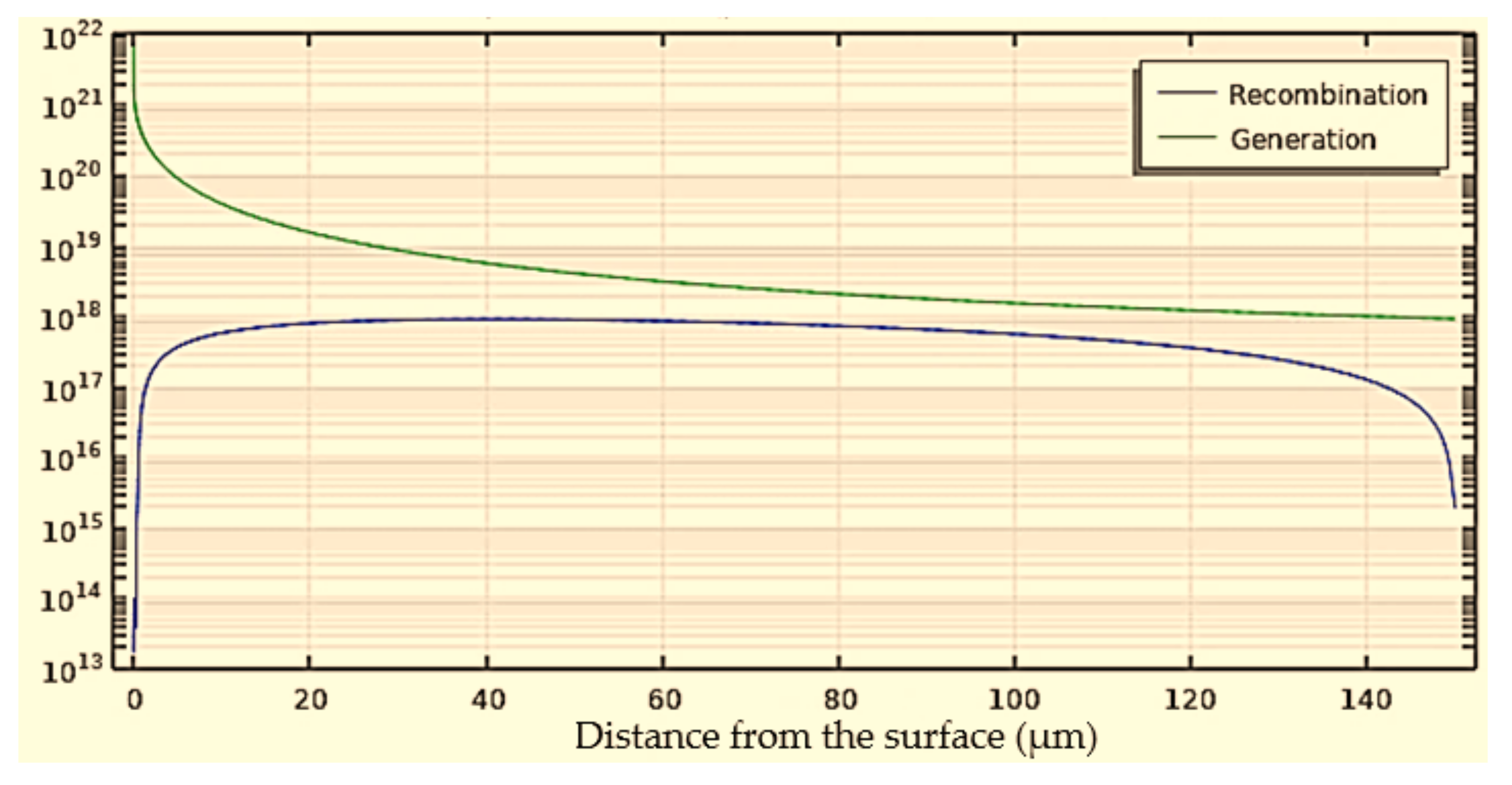
The generation and S-R-H recombination rates can also be found throughout the depth of the cell (Figure 12).
Moreover, I-V and P-V curves of the PV cell can also be characterized, referring to Figure 7.
COMSOL helps to adjust the properties of PV materials. such as light trapping, layer thickness, band structure, doping level, and many parameters that influence the obtained characteristics of PV cells. A theoretical model for GaAs-based solar cells with a p-i-n structure was analyzed by [44]. The influence of varying basic parameters on the obtained power was investigated using COMSOL Multiphysics. The mobilities of charge carriers were varied in combination with the lifetime of carriers and surface recombination velocity ‘SRV’. The results showed that higher PV efficiencies can be achieved by increasing the mobility and carriers’ lifetime while decreasing the surface recombination velocities [111,112,113]. Moreover, [31] developed a simulation model of PV modules in COMSOL Multiphysics to investigate the I-V and P-V characteristics of p-n junction space solar modules based on porous Si. The difference between the PV electrical characteristics COMSOL results and the experimental data obtained does not exceed 5%. Thus, the models developed by COMSOL help to investigate the electrical characteristics and establish the main factors affecting solar cell performance.
4. Summary and Outlook
To summarize, PV is the process of converting solar energy into electrical energy. Any PV system consists of solar cell arrays to deliver sufficient power. This paper covered many basics of solar cells, such as their working principle, design consideration, technical challenges in PV cells, employed materials, the significance of GaAs thin films in solar technology, their future prospects, and some mathematical analysis of p-n junction solar cells. The review also discussed the possibility of developing mathematical and numerical modelling of solar cells in MATLAB/Simulink and COMSOL Multiphysics to improve the PCE. The developed models help to investigate the (I-V) and (P-V) characteristics and determine the main parameters affecting the PV cell performance.
Author Contributions
Conceptualization, A.S.A.-E. and M.N.M.A.; writing—original draft preparation, A.S.A.-E.; writing and editing, M.N.M.A.; resources and funding acquisition, M.N.M.A. All authors have read and agreed to the published version of the manuscript.
Funding
Seeding Fund Research Grant (U-TV-RD-10-20) and UNITEN R&D Sdn. Bhd.
Institutional Review Board Statement
Not applicable.
Informed Consent Statement
Not applicable.
Data Availability Statement
Not applicable.
Acknowledgments
The authors would like to thank TNB Sdn.Bhd. for their support through Seeding Fund Research Grant (U-TV-RD-10-20) and UNITEN R&D Sdn. Bhd. in supporting this project.
Conflicts of Interest
The authors declare that no conflict of interest.
References
- Awasthi, A.; Shukla, A.K.; Murali Manohar, S.R.; Dondariya, C.; Shukla, K.N.; Porwal, D.; Richhariya, G. Review on sun tracking technology in solar PV system. Energy Rep. 2020, 6, 392–405. [Google Scholar] [CrossRef]
- Al-Ezzi, A. The market of solar panels in the United Kingdom. Appl. Sol. Energy 2017, 53, 78–84. [Google Scholar] [CrossRef]
- Nayak, P.K.; Mahesh, S.; Snaith, H.J.; Cahen, D. Photovoltaic solar cell technologies: Analysing the state of the art. Nat. Rev. Mater. 2019, 4, 269–285. [Google Scholar] [CrossRef]
- Mohammad Bagher, A. Types of Solar Cells and Application. Am. J. Opt. Photonics 2015, 3, 94–113. [Google Scholar] [CrossRef] [Green Version]
- Xing, Y.; Han, P.; Wang, S.; Liang, P.; Lou, S.; Zhang, Y.; Hu, S.; Zhu, H.; Zhao, C.; Mi, Y. A review of concentrator silicon solar cells. Renew. Sustain. Energy Rev. 2015, 51, 1697–1708. [Google Scholar] [CrossRef]
- Rathore, N.; Panwar, N.L.; Yettou, F.; Gama, A. A comprehensive review of different types of solar photovoltaic cells and their applications. Int. J. Ambient Energy 2019, 1–18. [Google Scholar] [CrossRef]
- Efaz, E.T.; Rhaman, M.M.; Imam, S.A.; Bashar, K.L.; Kabir, F.; Mourtaza, M.E.; Sakib, S.N.; Mozahid, F.A. A review of primary technologies of thin-film solar cells. Eng. Res. Express 2021, 3, 032001. [Google Scholar] [CrossRef]
- Gray, J.L. The Physics of the Solar Cell. In Handbook of Photovoltaic Science and Engineering; John Wiley & Sons, Ltd.: Chichester, UK, 2011; pp. 82–129. [Google Scholar]
- Almosni, S.; Delamarre, A.; Jehl, Z.; Suchet, D.; Cojocaru, L.; Giteau, M.; Behaghel, B.; Julian, A.; Ibrahim, C.; Tatry, L.; et al. Material challenges for solar cells in the twenty-first century: Directions in emerging technologies. Sci. Technol. Adv. Mater. 2018, 19, 336–369. [Google Scholar] [CrossRef] [PubMed]
- Shah, D.K.; KC, D.; Muddassir, M.; Akhtar, M.S.; Kim, C.Y.; Yang, O.B. A simulation approach for investigating the performances of cadmium telluride solar cells using doping concentrations, carrier lifetimes, thickness of layers, and band gaps. Sol. Energy 2021, 216, 259–265. [Google Scholar] [CrossRef]
- Physics of Semiconductor Devices. Mater. Today 2003, 6, 38. [CrossRef]
- Torchynska, T.V. III-V material solar cells for space application. Semicond. Phys. Quantum Electron. Optoelectron. 2002, 5, 63–70. [Google Scholar] [CrossRef] [Green Version]
- Gruginskie, N.; van Laar, S.C.W.; Bauhuis, G.; Mulder, P.; van Eerden, M.; Vlieg, E.; Schermer, J.J. Increased performance of thin-film GaAs solar cells by rear contact/mirror patterning. Thin Solid Films 2018, 660, 10–18. [Google Scholar] [CrossRef]
- Angadi, R.V. A Review on Different Types of Materials Employed in Solar Photovoltaic Panel. Int. J. Eng. Res. Technol. 2019, 7, 1–5. [Google Scholar]
- Neamen, D.A. Semiconductor Physics and Devices: Basic Principles; McGraw-Hill: New York, NY, USA, 2012. [Google Scholar]
- Smith, R.P.; Hwang, A.A.-C.; Beetz, T.; Helgren, E. Introduction to semiconductor processing: Fabrication and characterization of p-n junction silicon solar cells. Am. J. Phys. 2018, 86, 740–746. [Google Scholar] [CrossRef] [Green Version]
- Seeger, K. Semiconductor Physics; Springer Science & Business: Berlin/Heidelberg, Germany, 2013. [Google Scholar]
- Smets, A.H.M.; Jager, K.; Isabella, O.; van Swaaij, R.A.; Zeman, M. Solar Cell Parameters and Equivalent Circuit. Sol. Energy Phys. Eng. Photovolt. Convers. Technol. Syst. 2016, 113–121. [Google Scholar]
- Sze, S.M.; Ng, K.K. Photodetectors and Solar Cells. In Physics of Semiconductor Devices; John Wiley & Sons, Inc.: Hoboken, NJ, USA, 2006; pp. 663–742. [Google Scholar]
- Sharma, D.; Mehra, R.; Raj, B. Comparative analysis of photovoltaic technologies for high efficiency solar cell design. Superlattices Microstruct. 2021, 153, 106861. [Google Scholar] [CrossRef]
- Zhang, C.; Honsberg, C.; Faleev, N.; Goodnick, S. High Efficiency GaAs-Based Solar Cells Simulation and Fabrication; Arizona State University: Phoenix, AZ, USA, 2014. [Google Scholar]
- Radziemska, E. Thermal performance of Si and GaAs based solar cells and modules: A review. Prog. Energy Combust. Sci. 2003, 29, 407–424. [Google Scholar] [CrossRef]
- Floyd, T.L. Electronic Devices, 9th ed.; Pearson: London, UK, 2011. [Google Scholar]
- Arefeen, S.; Dallas, T. Low-cost racking for solar photovoltaic systems with renewable tensegrity structures. Sol. Energy 2021, 224, 798–807. [Google Scholar] [CrossRef]
- Wang, F.; Liu, X.-K.; Gao, F. Fundamentals of Solar Cells and Light-Emitting Diodes. In Advanced Nanomaterials for Solar Cells and Light Emitting Diodes; Elsevier: Amsterdam, The Netherlands, 2019. [Google Scholar]
- Willardson, R.K.; Beer, A.C. Semiconductors and Semimetals. In Semiconductors and Semimetals; Academic Press: Cambridge, MA, USA, 1966. [Google Scholar]
- Padmanabhan, B. Modeling of Solar Cells; Arizona State University: Phoenix, AZ, USA, 2008. [Google Scholar]
- Grundmann, M. The Physics of Semiconductors; Springer International Publishing: Cham, Switzerland, 2016. [Google Scholar]
- Please, C.P. An Analysis of Semiconductor P-N Junctions. 1982. Available online: http://imamat.oxfordjournals.org/ (accessed on 9 September 2021).
- Poole, C. Depletion Region Width Microwave Semiconductor Materials and Diodes. 2016. Available online: https://www.sciencedirect.com/topics/engineering/depletion-region-width (accessed on 9 September 2021).
- Shishkin, I.A.; Lizunkova, D.A.; Latukhina, N.V. Simulation of current-voltage characteristics and power-voltage characteristics of «space» solar cells based porous silicon in the Comsol Multiphysics package. J. Phys. Conf. Ser. 2019, 1410, 012096. [Google Scholar] [CrossRef]
- Loulou, M.; Turkestan, M.K.A.; Brahmi, N.; Abdelkrim, M. Current dependence of series and shunt resistances of solar cells. In Proceedings of the 2018 9th International Renewable Energy Congress (IREC), Hammamet, Tunisia, 20–22 March 2018; pp. 1–5. [Google Scholar] [CrossRef]
- Liang, K.; Ai, D.; Zhang, H.; Zhao, Y.; Zhang, Y.; Chen, H. Experimental performance analysis of the concentrated crystalline silicon solar cell—slicing cell. Sol. Energy 2021, 224, 1008–1016. [Google Scholar] [CrossRef]
- Saravanan, S.; Krishna Teja, T.; Dubey, R.S.; Kalainathan, S. Design and analysis of GaAs thin film solar cell using an efficient light trapping bottom structure. Mater. Today Proc. 2016, 3, 2463–2467. [Google Scholar] [CrossRef]
- Dzimano, G. Modeling of Photovoltaic Systems; Ohio State University: Columbus, OH, USA, 2008. [Google Scholar]
- Hamaguchi, C. Basic Semiconductor Physics; Springer-Verlag: Berlin, Germany, 2010; Volume 9. [Google Scholar] [CrossRef]
- Abbassi, R.; Abbassi, A.; Jemli, M.; Chebbi, S. Identification of unknown parameters of solar cell models: A comprehensive overview of available approaches. Renew. Sustain. Energy Rev. 2018, 90, 453–474. [Google Scholar] [CrossRef]
- Zekry, A.; Shaker, A.; Salem, M. Solar Cells and Arrays: Principles, Analysis, and Design; Elsevier: Amsterdam, The Netherlands, 2018; Volume 1. [Google Scholar]
- Ali, K.; Khalid, A.; Ahmad, M.R.; Khan, H.M.; Ali, I.; Sharma, S.K. Multi-junction (III–V) Solar Cells: From Basics to Advanced Materials Choices. In Solar Cells; Springer International Publishing: Cham, Switzerland, 2020; pp. 325–350. [Google Scholar]
- Moon, S.; Kim, K.; Kim, Y.; Heo, J.; Lee, J. Highly efficient single-junction GaAs thin-film solar cell on flexible substrate. Sci. Rep. 2016, 6, 30107. [Google Scholar] [CrossRef]
- Kayes, B.M.; Nie, H.; Twist, R.; Spruytte, S.G.; Reinhardt, F.; Kizilyalli, I.C.; Higashi, G.S. 27.6% Conversion efficiency, a new record for single-junction solar cells under 1 sun illumination. In Proceedings of the 2011 37th IEEE Photovoltaic Specialists Conference, Seattle, DC, USA, 19–24 June 2011; pp. 000004–000008. [Google Scholar] [CrossRef]
- Yamaguchi, M. III-V compound multi-junction solar cells: Present and future. Sol. Energy Mater. Sol. Cells 2003, 75, 261–269. [Google Scholar] [CrossRef]
- Verma, A.; Pethe, A. Modelling and Analysis of Multi-Junction Photovoltaic Cells. In Proceedings of the 17th India Council International Conference (INDICON), New Delhi, India, 10–13 December 2020. [Google Scholar] [CrossRef]
- Hossain, J. Design and simulation of double-heterojunction solar cells based on Si and GaAs wafers. J. Phys. Commun. 2021, 5, 085008. [Google Scholar] [CrossRef]
- Imran, A.; Sulaman, M.; Song, Y.; Eric, D.; Zahid, M.N.; Yousaf, M.; Saleem, M.I.; Li, M.; Li, D. Modeling and simulation of high-efficiency GaAs PIN solar cells. J. Comput. Electron. 2021, 20, 310–316. [Google Scholar] [CrossRef]
- Milanova, M.; Donchev, V.; Cheetham, K.J.; Cao, Z.; Sandall, I.; Piana, G.M.; Hutter, O.S.; Durose, K.; Mumtaz, A. Single-junction solar cells based on p-i-n GaAsSbN heterostructures grown by liquid phase epitaxy. Sol. Energy 2020, 208, 659–664. [Google Scholar] [CrossRef]
- Ko, T.S.; Lin, D.Y.; He, Y.C.; Kao, C.C.; Hu, B.Y.; Horng, R.H.; Wu, F.L.; Wu, C.H.; Tsai, Y.L. Optoelectric Properties of GaInP p-i-n Solar Cells with Different i-Layer Thicknesses. Int. J. Photoenergy 2015, 2015, 703045. [Google Scholar] [CrossRef]
- Sengupta, R.; Prashant, V.; Chakrabarti, T.; Sarkar, S.K. Modeling, simulation and comparative study of new compound alloy based P-I-N solar cells—An efficient way of energy management. In Proceedings of the 2015 International Conference on Power and Advanced Control Engineering (ICPACE), Bengaluru, India, 12–14 August 2015; pp. 86–89. [Google Scholar] [CrossRef]
- Al-Ezzi, A.; Abass, A. Selecting the Most Suitable Material for Punch Dies Using CES EduPack. In Proceedings of the 2018 2nd International Symposium on Multidisciplinary Studies and Innovative Technologies (ISMSIT), Ankara, Turkey, 19–21 October 2018; pp. 1–6. [Google Scholar] [CrossRef]
- Massiot, I.; Cattoni, A.; Collin, S. Progress and prospects for ultrathin solar cells. Nat. Energy 2020, 5, 959–972. [Google Scholar] [CrossRef]
- Hörantner, M.T.; Leijtens, T.; Ziffer, M.E.; Eperon, G.E.; Christoforo, M.G.; McGehee, M.D.; Snaith, H.J. The Potential of Multijunction Perovskite Solar Cells. ACS Energy Lett. 2017, 2, 2506–2513. [Google Scholar] [CrossRef]
- Yamamoto, K.; Yoshikawa, K.; Uzu, H.; Adachi, D. High-efficiency heterojunction crystalline Si solar cells. Jpn. J. Appl. Phys. 2018, 57, 08RB20. [Google Scholar] [CrossRef]
- Balaji, N.; Raval, M.C.; Saravanan, S. Review on Metallization in Crystalline Silicon Solar Cells. In Solar Cells; IntechOpen: London, UK, 2020. [Google Scholar] [CrossRef] [Green Version]
- Deshpande, R.A. Advances in Solar Cell Technology: An Overview. J. Sci. Res. 2021, 65, 72–75. [Google Scholar] [CrossRef]
- Roy, S.; Baruah, M.S.; Sahu, S.; Nayak, B.B. Computational analysis on the thermal and mechanical properties of thin film solar cells. Mater. Today Proc. 2021, 44, 1207–1213. [Google Scholar] [CrossRef]
- Yu, P.Y.; Cardona, M. Fundamentals of Semiconductors: Physics and Materials Properties; Springer: Berlin/Heidelberg, Germany, 2001. [Google Scholar]
- Rouway, M.; Boulahia, Z.; Chakhchaoui, N.; Fouzia, F.; El Hachemi Omari, L.; Cherkaoui, O.; Van Langenhove, L. Mathematical and numerical modelling of soiling effects of photovoltaic solar panels on their electrical performance. IOP Conf. Ser. Mater. Sci. Eng. 2020, 827, 012064. [Google Scholar] [CrossRef]
- Kawamoto, H. Electrostatic cleaning equipment for dust removal from soiled solar panels. J. Electrostat. 2019, 98, 11–16. [Google Scholar] [CrossRef]
- He, G.; Zhou, C.; Li, Z. Review of Self-Cleaning Method for Solar Cell Array. Procedia Eng. 2011, 16, 640–645. [Google Scholar] [CrossRef] [Green Version]
- Lee, T.D.; Ebong, A.U. A review of thin film solar cell technologies and challenges. Renew. Sustain. Energy Rev. 2017, 70, 1286–1297. [Google Scholar] [CrossRef]
- Qarony, W.; Hossain, M.I.; Hossain, M.K.; Uddin, M.J.; Haque, A.; Saad, A.R.; Tsang, Y.H. Efficient amorphous silicon solar cells: Characterization, optimization, and optical loss analysis. Results Phys. 2017, 7, 4287–4293. [Google Scholar] [CrossRef]
- Godt, J.; Scheidig, F.; Grosse-Siestrup, C.; Esche, V.; Brandenburg, P.; Reich, A.; Groneberg, D.A. The toxicity of cadmium and resulting hazards for human health. J. Occup. Med. Toxicol. 2006, 1, 22. [Google Scholar] [CrossRef] [PubMed] [Green Version]
- Ramanujam, J.; Singh, U.P. Copper indium gallium selenide based solar cells—A review. Energy Environ. Sci. 2017, 10, 1306–1319. [Google Scholar] [CrossRef]
- Mufti, N.; Amrillah, T.; Taufiq, A.; Sunaryono; Aripriharta; Diantoro, M.; Zulhadjri; Nur, H. Review of CIGS-based solar cells manufacturing by structural engineering. Sol. Energy 2020, 207, 1146–1157. [Google Scholar] [CrossRef]
- Frenzel, M.; Mikolajczak, C.; Reuter, M.A.; Gutzmer, J. Quantifying the relative availability of high-tech by-product metals—The cases of gallium, germanium and indium. Resour. Policy 2017, 52, 327–335. [Google Scholar] [CrossRef]
- Gul, M.; Kotak, Y.; Muneer, T. Review on recent trend of solar photovoltaic technology. Energy Explor. Exploit. 2016, 34, 485–526. [Google Scholar] [CrossRef] [Green Version]
- Papež, N.; Škvarenina, Ľ.; Tofel, P.; Sobola, D. Thermal stability of gallium arsenide solar cells. In Proceedings of the Photonics, Devices, and Systems VII, Prague, Czech Republic, 28–30 August 2017; 1060313, p. 27. [Google Scholar] [CrossRef]
- Pouladi, S.; Asadirad, M.; Oh, S.K.; Shervin, S.; Chen, J.; Wang, W.; Manh, C.N.; Choi, R.; Kim, J.; Khatiwada, D.; et al. Effects of grain boundaries on conversion efficiencies of single-crystal-like GaAs thin-film solar cells on flexible metal tapes. Sol. Energy Mater. Sol. Cells 2019, 199, 122–128. [Google Scholar] [CrossRef]
- Park, S.; Simon, J.; Schulte, K.L.; Ptak, A.J.; Wi, J.S.; Young, D.L.; Oh, J. Germanium-on-Nothing for Epitaxial Liftoff of GaAs Solar Cells. Joule 2019, 3, 1782–1793. [Google Scholar] [CrossRef]
- Rahaman, M.S.; Rahman, M.M.; Mise, N.; Sikder, M.T.; Ichihara, G.; Uddin, M.K.; Kurasaki, M.; Ichihara, S. Environmental arsenic exposure and its contribution to human diseases, toxicity mechanism and management. Environ. Pollut. 2021, 289, 117940. [Google Scholar] [CrossRef]
- Li, S.S. High-Speed III-V Semiconductor Devices. In Semiconductor Physical Electronics; Springer: New York, NY, USA, 2007; pp. 613–663. [Google Scholar]
- Cariou, R.; Benick, J.; Feldmann, F.; Höhn, O.; Hauser, H.; Beutel, P.; Razek, N.; Wimplinger, M.; Bläsi, B.; Lackner, D.; et al. III–V-on-silicon solar cells reaching 33% photoconversion efficiency in two-terminal configuration. Nat. Energy 2018, 3, 326–333. [Google Scholar] [CrossRef]
- Li, S.S. Semiconductor Physical Electronics; Li, S.S., Ed.; Springer: New York, NY, USA, 2006. [Google Scholar]
- Kasap, S.; Burr Ridge, B.; Dubuque, I.; Madison, I. New York San Francisco St. Louis Bangkok Bogotб Caracas Kuala Lumpur Lisbon London Madrid Mexico City Milan Montreal New Delhi Santiago Seoul Singapore Sydney Taipei Toronto, Principles of Electronic Materials and Devices Second Edition. 2006. Available online: www.mhhe.com (accessed on 9 September 2021).
- Masafumi Yamaguchi High-Efficiency GaAs-Based Solar Cells. In Post-Transition Metals; Rahman, I.M.M.; Asiri, A.M.; Tabbakh, T.A.; Khan, A. (Eds.) BoD—Books on Demand, Post-Transition Met: London, UK, 2020; p. 196. [Google Scholar]
- Papež, N.; Dallaev, R.; Ţălu, Ş.; Kaštyl, J. Overview of the Current State of Gallium Arsenide-Based Solar Cells. Materials 2021, 14, 3075. [Google Scholar] [CrossRef]
- Gulaliyev, M.G.; Mustafayev, E.R.; Mehdiyeva, G.Y. Assessment of Solar Energy Potential and Its Ecological-Economic Efficiency: Azerbaijan Case. Sustainability 2020, 12, 1116. [Google Scholar] [CrossRef] [Green Version]
- Chesnutt, J.K.W.; Guo, B.; Wu, C.Y. Numerical analysis of the effects of particle-particle interactions and particle size on the performance of an electrodynamic dust shield. J. Electrostat. 2019, 98, 58–68. [Google Scholar] [CrossRef]
- Kawamoto, H. Improved detachable electrodynamic cleaning system for dust removal from soiled photovoltaic panels. J. Electrostat. 2020, 107, 103481. [Google Scholar] [CrossRef]
- Kumar, S. Solar PV Performance-Issues and Challenges. 2014. Available online: www.ijireeice.com (accessed on 9 September 2021).
- Kawamoto, H.; Guo, B. Improvement of an electrostatic cleaning system for removal of dust from solar panels. J. Electrostat. 2018, 91, 28–33. [Google Scholar] [CrossRef]
- Zouaghi, A.; Zouzou, N. Numerical modeling of particle motion in traveling wave solar panels cleaning device. J. Electrostat. 2021, 110, 103552. [Google Scholar] [CrossRef]
- Karki, I.B. Effect of Temperature on the I-V Characteristics of a Polycrystalline Solar Cell. J. Nepal Phys. Soc. 2016, 3, 35. [Google Scholar] [CrossRef] [Green Version]
- Sun, C.; Xu, L.; Lai, X.; Li, Z.; He, M. Advanced Strategies of Passivating Perovskite Defects for High-Performance Solar Cells. Energy Environ. Mater. 2020, 4, 293–301. [Google Scholar] [CrossRef]
- Metaferia, W.; Schulte, K.L.; Simon, J.; Johnston, S.; Ptak, A.J. Gallium arsenide solar cells grown at rates exceeding 300 µm h−1 by hydride vapor phase epitaxy. Nat. Commun. 2019, 10, 3361. [Google Scholar] [CrossRef]
- Hussain, A.B.; Abdalla, A.S.; Mukhtar, A.S.; Elamin, M.; Alammari, R.; Iqbal, A. Modelling and simulation of single- and triple-junction solar cells using MATLAB/SIMULINK. Int. J. Ambient Energy 2017, 38, 613–621. [Google Scholar] [CrossRef]
- Zhang, Z.; Wu, J.; Wang, L.; Liu, F.; Jia, P.; Dai, L.; Lu, Y.; Bian, T. The analysis on simulation and invalidation of hot-spot temperature distribution in micro-defective crystalline silicon solar cells. Renew. Energy 2020, 147, 2218–2228. [Google Scholar] [CrossRef]
- Tayyaba, S.; Ashraf, M.W.; Tariq, M.I.; Akhlaq, M.; Balas, V.E.; Wang, N.; Balas, M.M. Simulation, analysis, and characterization of calcium-doped ZnO nanostructures for dye-sensitized solar cells. Energies 2020, 13, 4863. [Google Scholar] [CrossRef]
- Altermatt, P.P. Models for numerical device simulations of crystalline silicon solar cells—a review. J. Comput. Electron. 2011, 10, 314–330. [Google Scholar] [CrossRef]
- Üzüm, A.; Mandong, A.-M. Analysis of Silicon Solar Cell Device Parameters using PC1D. Sak. Univ. J. Sci. 2019, 1190–1197. [Google Scholar] [CrossRef] [Green Version]
- Markvart, T.; Castañer, L. Semiconductor Materials and Modelling. In Solar Cells; Elsevier: Amsterdam, The Netherlands, 2013; pp. 27–54. [Google Scholar]
- Sakib, S.; Abu, M.; Siddique, B. Modeling and Simulation of Solar Photovoltaic Cell for the Generation of Electricity in UAE. In Proceedings of the 2019 5th International Conference on Advances in Electrical Engineering (ICAEE), Dhaka, Bangladesh, 26–28 September 2019; pp. 66–71. [Google Scholar]
- Keshavani, K.; Joshi, J.; Trivedi, V.; Bhavsar, M. Issue 4. 2014. Available online: www.ijedr.org (accessed on 9 September 2021).
- Pandiarajan, N.; Muthu, R. Mathematical modeling of photovoltaic module with Simulink. In Proceedings of the 2011 1st International Conference on Electrical Energy Systems, Chennai, India, 3–5 January 2011; pp. 258–263. [Google Scholar]
- Shah, M.W.; Biate, R.L. Design and Simulation of Solar PV Model Using Matlab/Simulink. 2016. Available online: http://www.ijser.org (accessed on 9 September 2021).
- Gulomov, J.; Aliev, R.; Mirzaalimov, A.; Mirzaalimov, N.; Kakhkhorov, J.; Rashidov, B.; Temirov, S. Studying the Effect of Light Incidence Angle on Photoelectric Parameters of Solar Cells by Simulation. Int. J. Renew. Energy Dev. 2021, 10, 731–736. [Google Scholar] [CrossRef]
- Silvestre, S.; Chouder, A. Effects of shadowing on photovoltaic module performance. Prog. Photovolt. Res. Appl. 2008, 16, 141–149. [Google Scholar] [CrossRef]
- Selmi, T.; Belghouthi, R. A novel widespread Matlab/Simulink based modeling of InGaN double hetero-junction p-i-n solar cell. Int. J. Energy Environ. Eng. 2017, 8, 273–281. [Google Scholar] [CrossRef] [Green Version]
- Haschke, J.; Dupré, O.; Boccard, M.; Ballif, C. Silicon heterojunction solar cells: Recent technological development and practical aspects—from lab to industry. Sol. Energy Mater. Sol. Cells 2018, 187, 140–153. [Google Scholar] [CrossRef]
- Nguyen, X.H.; Nguyen, M.P. Mathematical modeling of photovoltaic cell/module/arrays with tags in Matlab/Simulink. Environ. Syst. Res. 2015, 4, 24. [Google Scholar] [CrossRef]
- Das, N.; Wongsodihardjo, H.; Islam, S. Modeling of multi-junction photovoltaic cell using MATLAB/Simulink to improve the conversion efficiency. Renew. Energy 2015, 74, 917–924. [Google Scholar] [CrossRef]
- Kumar Srivastav, A.; Kumar Gupta, A.; Raj Jaiswal, R.; Kumar Gupta, S. Modelling and Simulation of Photo voltaic System Using Matlab/Simulink. J. Phys. Conf. Ser. 2020, 1579, 012024. [Google Scholar] [CrossRef]
- Vengatesh, R.P.; Rajan, S.E. Investigation of cloudless solar radiation with PV module employing Matlab-Simulink. Sol. Energy 2011, 85, 1727–1734. [Google Scholar] [CrossRef]
- Comsol, Si Solar Cell 1D. Available online: www.comsol.com/trademarks (accessed on 9 September 2021).
- Mahakud, D.S.J.J. Numerical Modeling of P-i-N Solar Cell. 2014. Available online: https://www.comsol.com/paper/numerical-modeling-of-p-i-n-solar-cell-19367 (accessed on 9 September 2021).
- Abdellatif, O.; Mahmoud, I.M.; Abdellatif, S.O.; Abdelsalam, T.S. Numerical Modeling and Integration of a PV System Using Finite Element Method. 2015. Available online: https://www.researchgate.net/publication/275099199 (accessed on 9 September 2021).
- Reference Air Mass 1.5 Spectra/Grid Modernization/NREL. Available online: https://www.nrel.gov/grid/solar-resource/spectra-am1.5.html (accessed on 9 September 2021).
- Ranabhat, K.; Patrikeev, L.; Antal’evna-Revina, A.; Andrianov, K.; Lapshinsky, V.; Sofronova, E. An introduction to solar cell technology. Istraz. Proj. Privredu 2016, 14, 481–491. [Google Scholar] [CrossRef] [Green Version]
- Zimmerman, W.B.J. Introduction to Comsol Multiphysics. 2006, pp. 1–26. Available online: https://cdn.comsol.com/doc/5.5/IntroductionToCOMSOLMultiphysics.pdf (accessed on 9 September 2021).
- COMSOL Multiphysics® Introduction to the Semiconductor Module. 2017. Available online: https://doc.comsol.com/5.6/doc/com.comsol.help.semicond/IntroductionToSemiconductorModule.pdf (accessed on 9 September 2021).
- Andreani, L.C.; Bozzola, A.; Kowalczewski, P.; Liscidini, M.; Redorici, L. Silicon solar cells: Toward the efficiency limits. Adv. Phys. X 2019, 4, 1548305. [Google Scholar] [CrossRef] [Green Version]
- Shao, G. Work Function and Electron Affinity of Semiconductors: Doping Effect and Complication due to Fermi Level Pinning. Energy Environ. Mater. 2021, 4, 273–276. [Google Scholar] [CrossRef]
- Li, X.; Xu, Q.; Yan, L.; Ren, C.; Shi, B.; Wang, P.; Mazumdar, S.; Hou, G.; Zhao, Y.; Zhang, X. Silicon heterojunction-based tandem solar cells: Past, status, and future prospects. Nanophotonics 2020, 10, 2001–2022. [Google Scholar] [CrossRef]
Figure 1.
A p-n junction PV cell.

Figure 2.
The basic components of a PV system.

Figure 3.
The basic semiconductor form at the instant connection of the p-n sections and generating the electric field in the space charge region.
Figure 3.
The basic semiconductor form at the instant connection of the p-n sections and generating the electric field in the space charge region.

Figure 4.
The flow of majority carriers in a forward-biased diode.

Figure 5.
The PV cell under illumination.

Figure 6.
The practical equivalent circuit of a solar cell.

Figure 7.
(I-V) and (P-V) characteristics of a solar cell under illumination.

Figure 8.
The structure of valence electrons of Ga and As atoms.

Figure 9.
(a) Effect of radiation intensity effect on the P-V characteristics of single-junction GaAs solar cells. (b) Temperature effect on the P-V curve of single-junction GaAs PV cells under AM 1.5 condition.
Figure 9.
(a) Effect of radiation intensity effect on the P-V characteristics of single-junction GaAs solar cells. (b) Temperature effect on the P-V curve of single-junction GaAs PV cells under AM 1.5 condition.

Figure 10.
The impact of (a) series resistance (b) shunt resistance on the P-V characteristics of single-junction GaAs cells under AM 1.5 condition.
Figure 10.
The impact of (a) series resistance (b) shunt resistance on the P-V characteristics of single-junction GaAs cells under AM 1.5 condition.

Figure 11.
Doping profile beneath the surface.

Figure 12.
Generation and recombination rates through the thickness of the device.


Table 1.
A comparison between the typical types of materials used in PV solar cells.
| Material | Sub-Material | PCE | Advantages | Problems |
|---|---|---|---|---|
| c-Si | Single crystal | 20% [53] | ||
| Polycrystal | 16% [60] | Cost-effective as compared to the monocrystalline module [54]. | ||
| Thin Films | a-Si | 11.3% [61] | ||
| CdTe/CdS | 18.3% [10] | |||
| CIS/CIGS | 22.8% [63] |
| In and Ga sources are limited [65]. | |
| GaAs | Over 30% [66] |
Publisher’s Note: MDPI stays neutral with regard to jurisdictional claims in published maps and institutional affiliations. |
© 2022 by the authors. Licensee MDPI, Basel, Switzerland. This article is an open access article distributed under the terms and conditions of the Creative Commons Attribution (CC BY) license (https://creativecommons.org/licenses/by/4.0/).
Share and Cite
MDPI and ACS Style
Al-Ezzi, A.S.; Ansari, M.N.M. Photovoltaic Solar Cells: A Review. Appl. Syst. Innov. 2022, 5, 67. https://doi.org/10.3390/asi5040067
AMA Style
Al-Ezzi AS, Ansari MNM. Photovoltaic Solar Cells: A Review. Applied System Innovation. 2022; 5(4):67. https://doi.org/10.3390/asi5040067
Chicago/Turabian StyleAl-Ezzi, Athil S., and Mohamed Nainar M. Ansari. 2022. "Photovoltaic Solar Cells: A Review" Applied System Innovation 5, no. 4: 67. https://doi.org/10.3390/asi5040067