Article

Overcoming Variability in Printed RF: A Statistical Method to Designing for Unpredictable Dimensionality

1
Department of Electrical and Computer Engineering, University of Massachusetts Lowell, 40 University Avenue, Lowell, MA 01854, USA
2
U.S. Army Combat Capabilities Development Command Soldier Center, General Greene Avenue, Natick, MA 01760, USA
*
Author to whom correspondence should be addressed.
Designs 2022, 6(1), 13; https://doi.org/10.3390/designs6010013
Submission received: 18 December 2021 / Revised: 27 January 2022 / Accepted: 30 January 2022 / Published: 5 February 2022
(This article belongs to the Special Issue 3D Printing Functionality: Materials, Sensors, Electromagnetics)

Abstract

:
As additively manufactured radio frequency (RF) design expands towards higher frequencies, performance becomes ever more sensitive to print-induced dimensional variations. These slight deviations from design dimensions typically skew RF performance, resulting in low yields or poor device performance. In order to overcome this limitation, RF design paradigms must be developed for non-uniform process and material-specific variations. Therefore, a new generalized approach is developed to explore variation-tolerant designs for printed RF structures. This method evaluates the feature fidelity and S11 performance of micro-dispensed, X-band (8–12 GHz) patch antennas by evaluating the standard deviation in as-printed features, surface roughness, and thickness. It was found that the traditional designs based on optimal impedance matching values did not result in the most robust performance over multiple printing sessions. Rather, performance bounds determined by print deviation could be utilized to improve large-batch S11 results by up to 7 dB. This work demonstrates that establishing the average standard deviation of printed dimensions in any RF printing system and following the formulated design procedure could greatly improve performance over large datasets. As such, the method defined here can be applied to improve large-scale, printed RF yields and enable predictive performance metrics for any given printing method.

Graphical Abstract

1. Introduction

As additive manufacturing (AM) technology pushes towards applications at 5G and beyond, it becomes necessary to investigate the repeatability of direct-write (DW) manufacturing methods with respect to high-throughput manufacturing [1,2,3]. The wide array of printing methods and materials used in DW electronics corresponds to both variable feature resolution within a single structure and between multiple structures within a production batch. Therefore, a generalized design method must be explored to compensate for both fabrication variability and to maximize production yields. As such, this work explores a design process to transition common printed RF systems from low-yield single-run structures towards high-yield production. Thus, a method is developed that can produce reliable RF structures despite significant dimensional variability.
The advantages of AM techniques have broadened on-demand design capabilities across multiple industries ranging from biomedical to communications. DW manufacturing in particular has expanded rapidly alongside increasing demand or flexible, embedded, and low-cost electronic components. Benefits of DW processes have encouraged a variety of deposition methods including micropen dispensing [4,5], aerosol jetting [6,7], ink jetting [8,9,10,11,12,13], stereolithography [14,15,16], and metal embedding [17,18,19,20,21,22]. These methods can utilize materials as varied as metals, plastics [23], battery materials [24,25], and even organics [26]. DW electronics have been heavily investigated in sensing applications: using conductive inks for capacitive-based sensing of moisture and humidity levels [27,28], gas exposure [29], and pressure and material wear sensing [30,31]. Many of these traditional DW applications can be enhanced through the integration of wireless communication and, as such, there has also been research combining DW sensors with flexible RFID tags [8,32,33] and WLAN frequency band antennas optimal for IoT devices [34]. Additionally, printed inductors, capacitors, transducers, energy harvesting rectennas, and low loss dielectrics have all been developed specifically for RF applications [35,36,37,38]. Work is also being undertaken to implement these RF components on flexible, foldable, and conformal surfaces [32,39,40,41].
While some work has been done fabricating high frequency printed components, such as 5 GHz transistors [11], 5 GHz phased array antennas [40], and Ultra-wideband antennas ranging up to 10 GHz [10], these studies do not include an evaluation on acceptable tolerances, variations, or design metrics for high volume manufacturing. It has been shown that some of the inherent inconsistencies introduced by DW methods, such as overlapping lines, overspray, and varying trace thicknesses do not necessarily degrade MHz RF performance [33]; however, feature resolution is expected to have a much larger effect on RF performance as feature sizes decrease. In order to maintain performance comparable to traditionally manufactured RF structures while moving into the X and Ku bands, designs must be revised to counteract or otherwise adapt for the unpredictable effects of printing. The unpredictable dimensionality of printing is expected to translate into unpredictable effects on the RF impedance matching, and therefore unpredictable RF performance. Thus, it becomes difficult to predict experimental, printed performance without in-depth analysis of dimensional characterization, re-simulation, and experimental verification. Based on the design methods in this work, our conclusions can be adapted towards printed deviations in more complex antenna and photonic designs such as statistical calibrations, polarization conversion, or multiple patches [42,43,44]. However, as system complexity increases tools such as machine learning maybe required to determine a variability invariant design.
Finally, initial work has been done on using machine learning (ML) training algorithms within AM to predict optimal processing and material parameters for high print fidelity, for example in extrusion-based bio-printing [45,46] ML has also been used to establish models for predicting behavior of printed systems based on print parameters, such as determining the expected conductivity of jet-printed biosensors [47]. While these studies focus on exploiting ML to determine the best available print parameters for high print fidelity or specific component characteristics, no work has assessed how quantifying the variability within a single set of print parameters can be harnessed to predict overall performance despite imperfect resolution. The initial data set provided in this work will be presented in a way that can be adapted to produce ML training sets by comparing measured feature dimensions with expected performance. It is the hope that this work will inspire ML models in order to select the ideal set of component dimensions for the highest manufacturing yield and enable predictive performance through ML.

2. Materials and Methods
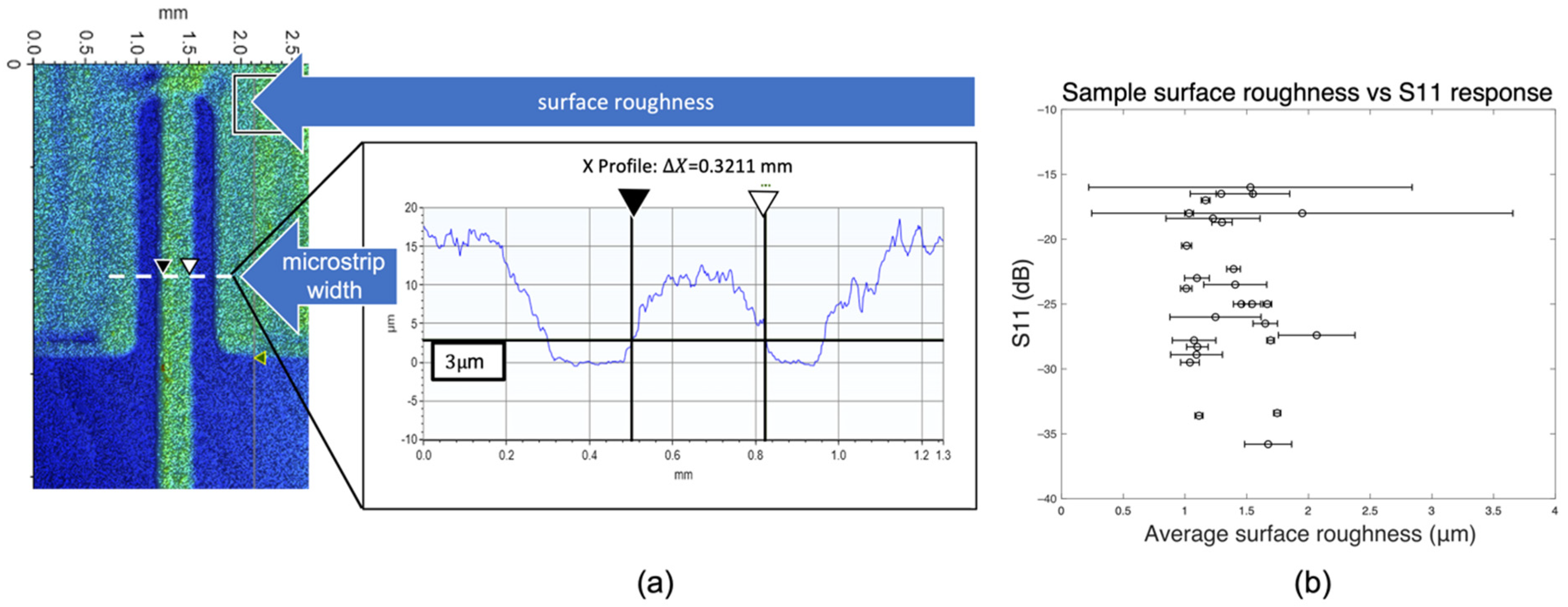
As an assessment of using characterized print variations to improve the design process and performance of printed RF, this work utilizes a set of common, printable RF structures, materials, and tooling. Specifically, the micropen dispenser (Nordson EFD, East Providence, RI, USA) was used to deposit one of the most common printable inks, DuPont CB028 (Dupont, Wilmington, DE, USA). To remove dielectric variability from our analysis, I-Tera MT40 RF laminate (Isola Laminate Group, Chandler, AZ, USA) with a 1 oz copper ground plane was used as a substrate material. A microstrip fed patch antenna with impedance matching slits was designed, simulated, and printed. The patch antenna is one of the most common structures in printed RF and, thus, enables the results of this work become applicable to a variety of application spaces.

2.1. Antenna Design

CST Microwave Studio (Dassault Systems) was used to design the microstrip fed patch antenna optimized for an 8 GHz resonance and a 50 Ω input impedance. A traditional copper version was designed as a control sample and a separate as-printed silver design was used for the DW version. Both copper and printed samples used I-Tera MT40 substrates with 1 oz copper ground planes, 0.127 mm dielectric thickness, dielectric constant (Dk) of 3.45 and loss tangent of 0.0031.
Initial antenna testing (copper-clad, CNC-milled, PCB antennas) confirmed the dielectric constant of the Isola I-Tera MT40 substrate. Additionally, it was confirmed through simulation that the same magnitude of dimensional variations in microstrips printed on substrates between 3.45 +/−0.5 Dk exhibited only difference in approx. +/−0.6 Ω in reference impedance. Therefore, any realistic variations of dielectric constant, such as altering substrate material, will have little effect on printed variability versus RF performance. However, as dielectric thickness decreases, the same process variability will have a much more significant effect on RF performance. For example, the same printing variability (+/−40 μ m ) on a microstrip line produces characteristic impedance of +/−1.2 Ω with a dielectric thickness of 0.381 mm and +/−5 Ω with a dielectric thickness of 0.127 mm. As AM techniques trend towards thinner, more flexible substrates, a 0.127 mm thickness highlights both more significant variation effects and more accurately represents the constraints of printed RF systems when adopted into hybrid/flexible form factors.
Using Equations (1) and (2), The initial microstrip width W for both designs was chosen as 300 μm by setting Z 0 in Equation (1) equal to 50 Ω, where H is the dielectric thickness (0.127 mm), and ε r is the dielectric constant (3.45). To further refine the design, simulations were utilized to determine the length of the microstrip inset into the patch, henceforth referred to as the inlet length (3100 μm for copper and 2600 μm for printed silver), and the width of the adjacent inset channels, henceforth referred to as the inlet width (200 μm for both designs).
Z 0 = 120 π ε e f f [ W H + 1.393 + 2 3 ln ( W H + 1.444 ) ]
ε e f f = ε r + 1 2 + ε r 1 2 1 + 12 ( W H )
The conductivity of the silver nanoparticle ink in this work was measured using a 4-point probe measurement as approximately 3.45 × 10⁶ S/m when sintered at 160 °C for 1 h. This value is similar to the conductivity reported in literature using similar sintering parameters [48]. As RF design is generally moving towards thinner substrates, a 0.127 mm substrate was chosen as a trade-off between manufacturability and analysis.
All designs were laid out as DXF files in AutoCad (Autodesk Inc., San Rafael, CA, USA). CNC Milling of the copper design was performed on the Accurate CNC 737 (Accurate CNC, Inc. Fort Wayne, Indiana) using a 5 mil end mill bit (Midwest Circuit Technology, Aurora, OH, USA). DW printing of the silver design was performed on a Nordson Pro4 micropen system (Nordson EFD, East Providence, RI, USA) using Dupont CB028 conductive silver ink.

2.2. Direct-Write Fabrication
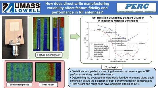
Changes in deposition pressure, speed, tip gauge, and tip distance from the substrate were used to produce a range of variation in both feature size and feature deviation. These variations enable investigation of the relationship between fidelity and performance. When transitioning this method to other materials or tooling, the variation in the specific printing process must be characterized at optimal print parameters. All printed structures were compared to simulated structures (CST Microwave Studio) and CNC milled, dual-clad copper control samples in order to validate the legitimacy of the simulation model. Adherence to the model dimensions and print integrity (surface roughness, gaps, air bubbles, etc.) were examined using a variety of measurement tools including optical microscopy and profilometry. The measured value of each printed feature was then plotted separately against the S11 performance for all antennas in the dataset and compared to simulation models of the S11 response for the measured features. Finally, an updated set of design dimensions was developed which compensates for the levels of experimental print variation and experimental S11 resonance depth.
The aforementioned speed and pressure settings were also systematically analyzed to determine a minimum achievable uniform trace width of approximately 120 μm for our printing system. The DXF files were serpentine raster filled using trace width settings ranging from 170 μm to 120 μm, and minimum-maximum trace overlap allowances of 10–50% or 10–20%. Print parameters utilizing speeds of 2–9 mm/s, pressures of 22 to 35 PSI, and tip gauges of 30 or 32 were combined with overlap and trace width settings to produce a set of 27 acceptable printed antennas. For all printed designs the top copper cladding layer was removed using Ferric Chloride etching (CE-100, Transene Company, Inc., Danvers, MA, USA) and no further surface functionalization was required before printing. Both printed and CNC milled control samples were tested with a 50 Ω Pasternack 0.2032 mm PCB launch SMA connectors (Infinite Electronics International, Inc., Irvine, CA, USA).
The printed antennas were cured and sintered at 160 °C for 1h before a Bruker GT-K Optical Profilometer (Bruker Nanosurfaces, Tucson, AZ, USA) was used to analyze five feature sizes per antenna: waveguide width, inlet width and length, sample height, surface roughness.
One port S-parameters were measured for all samples using a Keithley PNA Network Analyzer N5225A (Keithley Instruments, Cleveland, OH, USA). The results were recorded alongside the average printed dimensions and feature standard deviation as determined by optical profilometry.

3. Results

The printed antenna systems were evaluated independently over five features. These features are as follows: printed material thickness, surface roughness, microstrip width, impedance matching inlet width, and impedance matching inlet length. Using these five parameters, it was possible to develop a design method to compensate for non-ideal feature sizes over all print regions of a patch antenna. Although printed variations in patch size do affect antenna performance through slight, predictable resonance frequency shifts, a much larger performance effect was observed in impedance matching dimensions. As such the analysis focuses on optimizing impedance matching constraints in the antenna system.

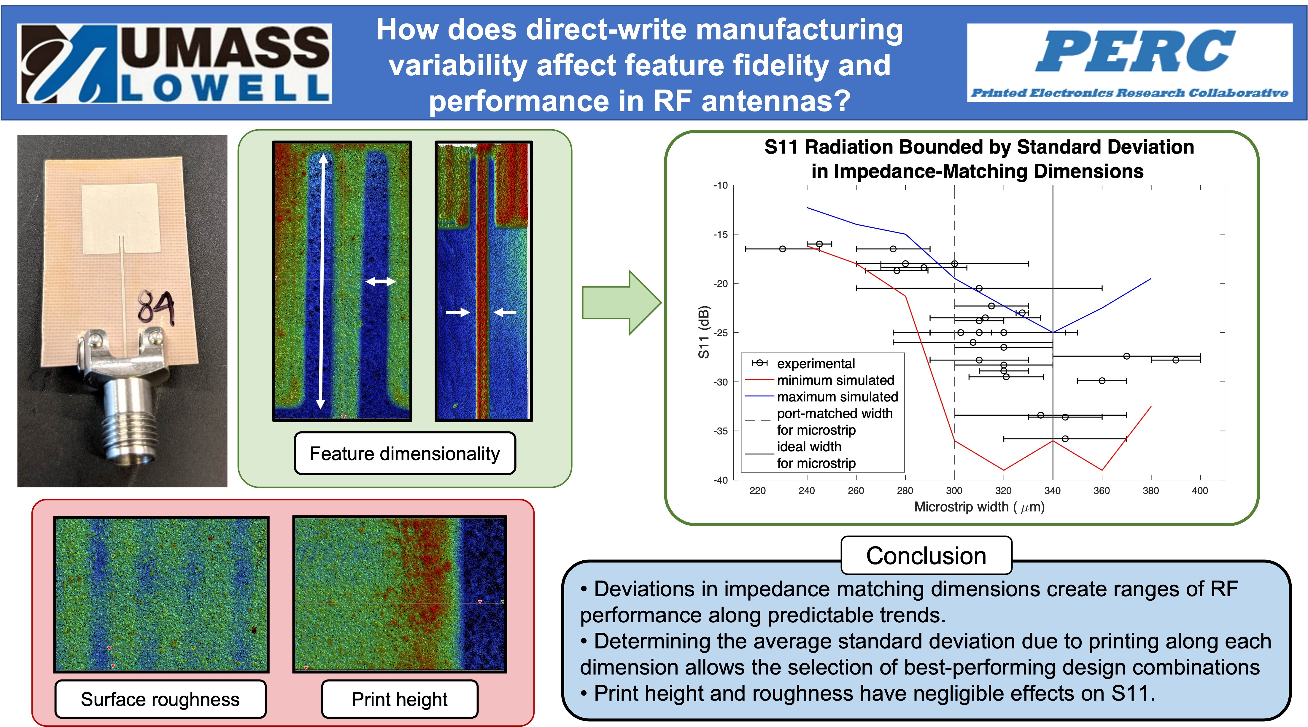
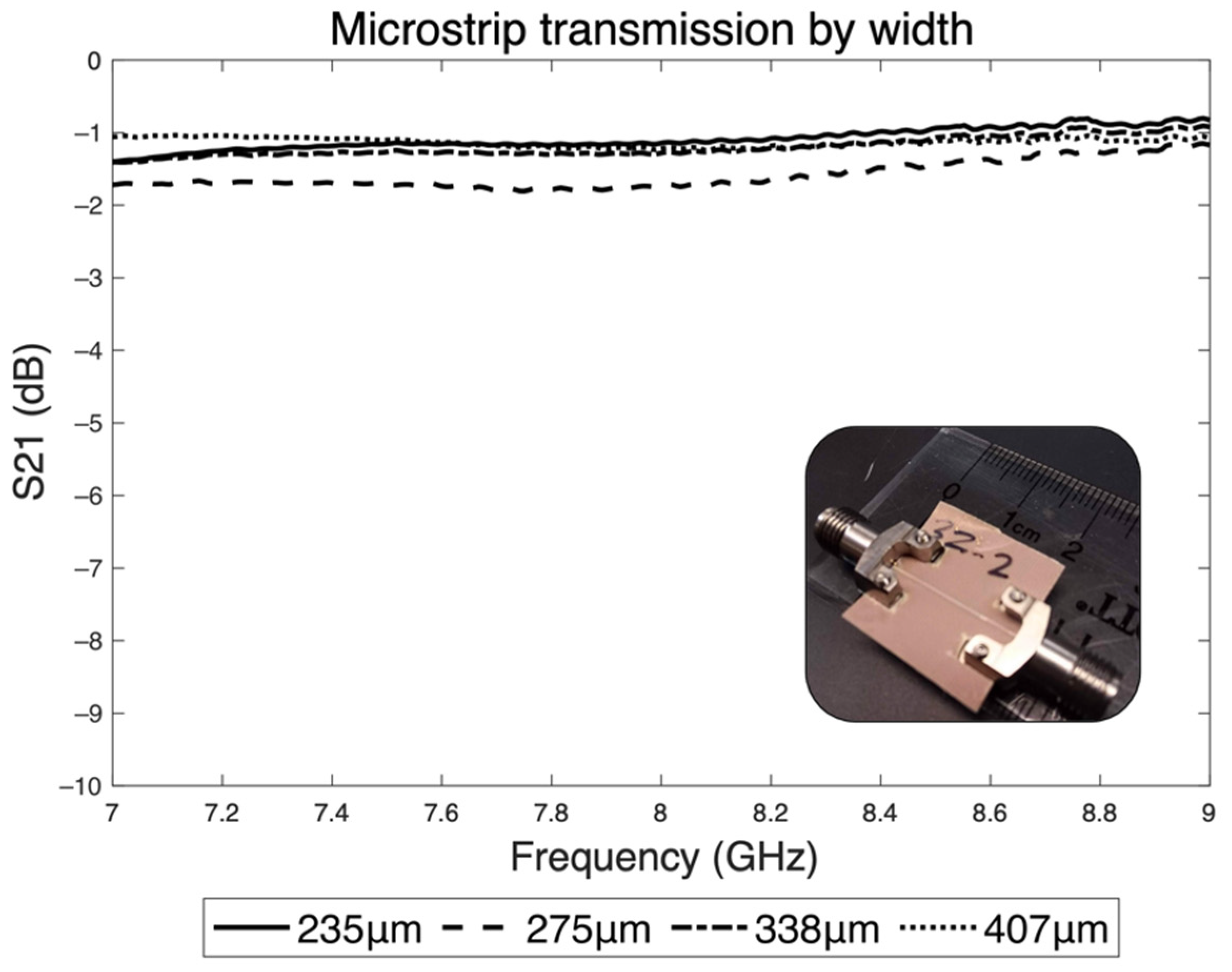
3.1. Printed Material Thickness and Surface Roughness

Optical microscopy and optical profilometry were used to measure a variety of feature dimensions ranging from overall sample height to patch surface roughness. It was observed that printed form factors generally have a more variable roll-off on the print edge than those produced using traditional milling or etching techniques. For this reason, one must determine a consistent method for selecting start and end measurements points for a feature. Using a relative permeability μ r = 0.9998 and the measured CB028 resistivity ρ = 2.9   Ωm, the skin depth δ = 3   μm of the printed silver can be found using Equation (3):
δ = ρ π f 0 μ 0 μ r ;   μ 0 = 4 π E 7
Therefore, feature measurements were taken starting at a height of 3μm as shown on the cross section of a microstrip line in Figure 1a.
It was determined that feature sizes with a thickness less than the skin depth do not significantly influence the resulting RF performance. Thus, this work utilized the skin depth as both a “cut-off” when measuring dimensions, as well as a minimum required thickness of the overall print. Indications of a relationship between S11 response and dimensional variation can be observed in Figure 1b. Due to the low surface roughness with respect to wavelength, no significant S11 variation was seen when varying sample heights and/or surface roughness. This result was to be expected and provides a good initial starting point to a printed design.

3.2. Variability in Printed RF Features

Antenna performance was assessed through the S11 network parameter which characterizes the reflection coefficient of a transmitting antenna. Additionally, two different aspects of feature variability were analyzed: (1) variation in average feature size from design and (2) standard deviation of a feature dimension from its average. These two types of variability were then measured over three printed features: (1) microstrip width, (2) impedance matching inlet width, and (3) impedance matching inlet length. The influence of each dimension on performance was first assessed by plotting the average dimension and standard deviation against the respective sample’s experimental S11 response at a resonance of, 8 GHz +/−0.12 GHz. Figure 2 shows S11 as a function of as-printed dimensions: (b) microstrip width, (c) inlet width, and (d) inlet length. Error bars indicate +/−1 standard deviation in the as-printed parameters, and theoretically ideal design dimensions are shown on each plot as a dashed line. Indications of a relationship between S11 response and dimensional variation can be observed for the microstrip width and the impedance matching inlet width.
While Figure 2 does imply a trend in S11 based on the variations of a single dimension, the majority of antennas in the dataset have multiple dimensions which deviate from design parameters, and some antennas perform very well even with multiple deviating parameters. Thus, these dimensions are not individually a pure indicator of S11 performance. For example, S11 appears to improve for deviations in inlet widths narrower than the designed value of 200 μm (Figure 2c). However, in a printed form-factor the same effects that increase microstrip width will also narrow inlet width, thus this performance improvement is correlated with at least two changing feature dimensions on the same sample. In other words, print variations simultaneously alter the transmission line characteristic impedance and antenna impedance matching inlets. These deviations result in significantly altered structural dimensions in some cases improving performance and in other cases degrading performance. Therefore, producing the most consistent RF design is dependent on determining the effects of as-printed dimensional combinations which stem from variations in multiple feature dimensions. To accomplish this feat, we must reduce the degrees of freedom to only those that most significantly influence performance.

4. Discussion: Determining Design Metrics

To determine the combined variability effects within the system, one must first determine the variability in each individual feature. To this end, the following section analyzes the microstrip transmission line, impedance matching inlet width, and impedance matching inlet length to produce a predictive model encompassing all significant feature variability with respect to the printed microstrip variability.

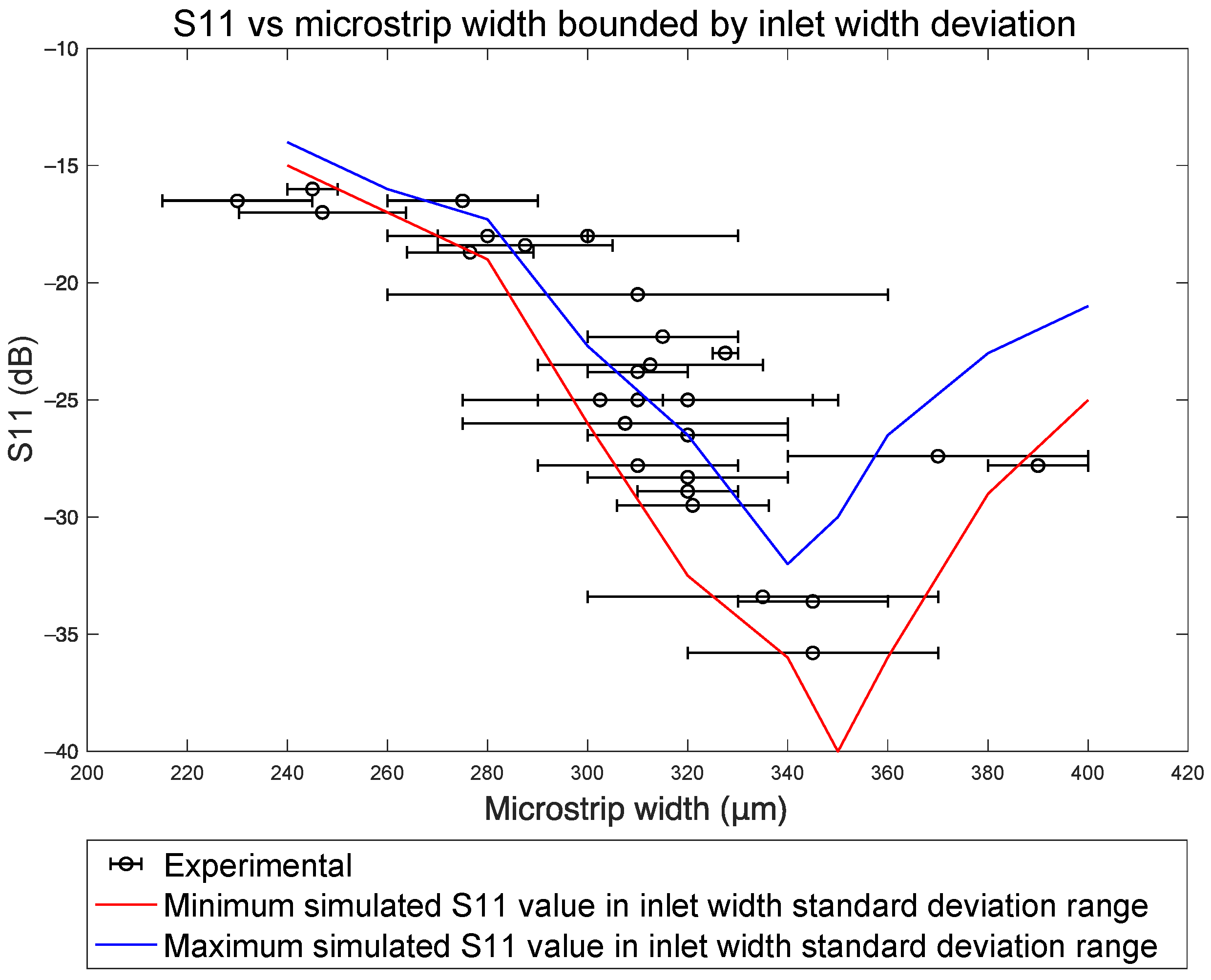
4.1. Microstrip Width Metrics

A set of microstrip lines 18 mm in length and spanning widths of 235   μ m to 407   μ m, were printed to determine the effects of variation on overall transmission line performance. From Equation (1) this variation translates to characteristic impedances ranging from 60 Ω to 40 Ω respectively. S21, or transmission, was measured from 7 to 9 GHz between two 50 Ω ports for each printed microstrip. All transmission lines displayed S21 values of >−2 dB at 8 GHz (Figure 3). This result suggests that this level of variation in printed microstrip width has no significant, independent effect on antenna S11 values.
Contrastingly, in Figure 2b antenna S11 performance does display a clear trend between microstrip width and resonance depth. However, a unique aspect of the printed form factor is that changing microstrip width will also create an inherent variation in the impedance matching inlet width and length, as all features are printed concurrently. Therefore, a variation in microstrip width will alter both the characteristic impedance of the microstrip and the ability of the matching features to operate as intended. This result affords a unique opportunity to evaluate both impedance matching inlet width and length with respect to microstrip width. Thus, this work can develop a characterization method which can combine all feature variabilities with respect to each other.

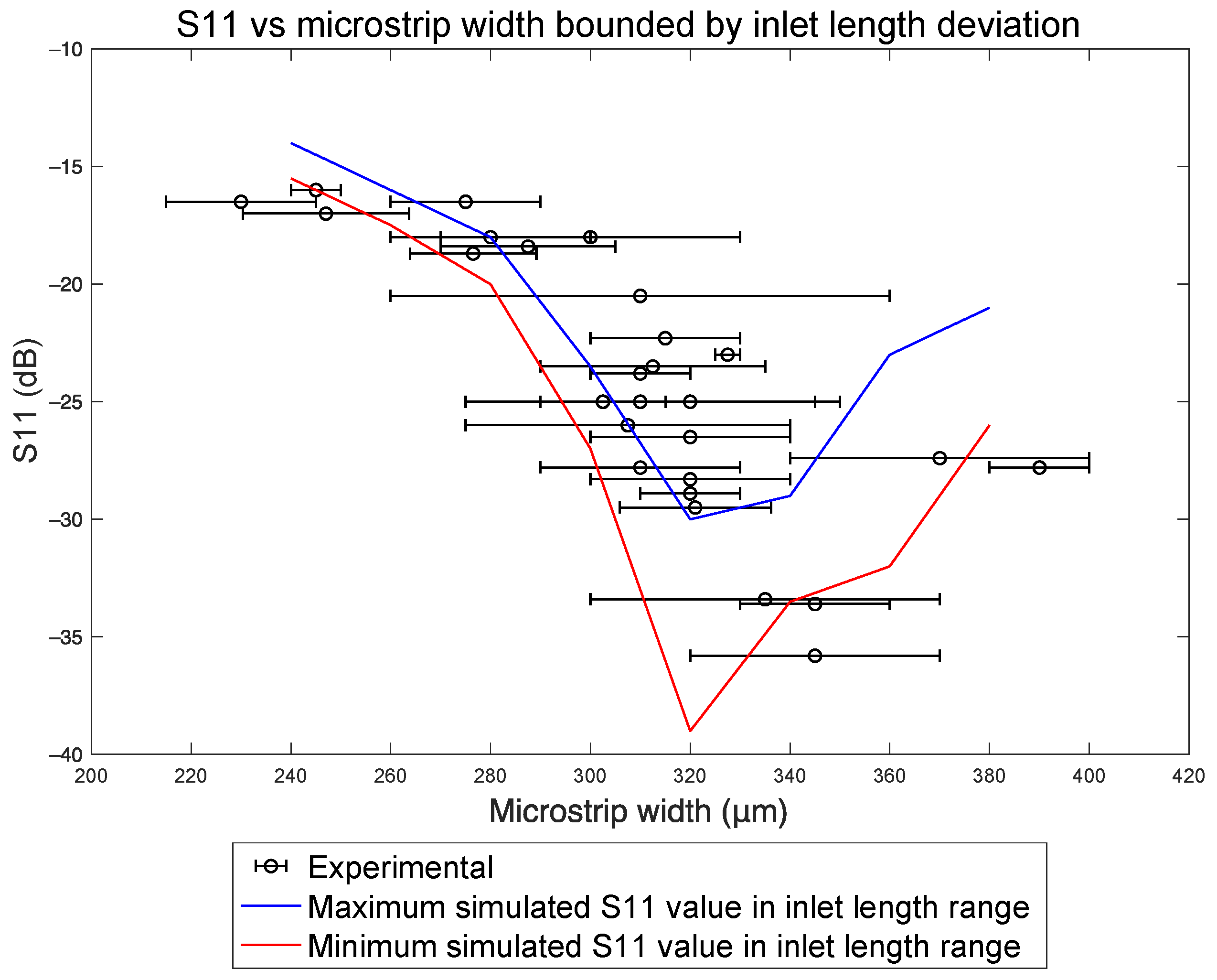
4.2. Impedance Matching Inlet Width and Inlet Length

To assess the individual contributions of changing inlet width and inlet length on antenna performance, a set of simulations were performed holding all other dimensions constant at their designed values, while allowing the inlet dimension of interest to vary along one standard deviation of the experimentally measured range. For inlet width assessment, the microstrip width was held at 300 μm, the inlet length held at 2.6 mm, and the inlet width swept from 100 μm to 260 μm. For inlet length, the microstrip width was held at 300 μm, the inlet width held at 200 μm, and the length swept across 2.42 mm to 2.6 mm. In each case, the simulated data was plotted and overlayed with the experimental data in Figure 2c,d. The poor fit of the simulation data to the experimental results illustrates that are not solely responsible for S11 performance are also not solely responsible for S11 performance variations.
To combine the effects of variation in each inlet dimension respectively with microstrip width variation, a series of simulations were performed by examining all inlet dimension values within one standard deviation of the average print-to-print value (170+/−30 μm) at successive microstrip widths, while the other inlet dimension remained constant at the designed value. The best performing S11 results (most negative) were plotted together as a lower-bound and the worst performing (least negative) S11 results plotted together as an upper-bound. The bounds of inlet width variation across microstrip width can be seen in Figure 4, and the inlet length variation bounds can be seen in Figure 5. The spacing between the two bounds in both figures illustrates that the effects of variation in each dimension are not constant across the entire microstrip width range. For example, in Figure 4, the difference between best and worst performing S11 simulation results for a 260 μm microstrip was significantly smaller than the same in bounds of a 350 μm microstrip.
As neither Figure 4 nor Figure 5 completely capture the dataset, it is necessary to consider concurrent variability in all three measured dimensions in order to predictively characterize the experimental data. This result is expected; as mentioned previously, variability in one printed dimension corresponds to a related variability in other printed dimensions. The full characterization is presented in Section 4.3.

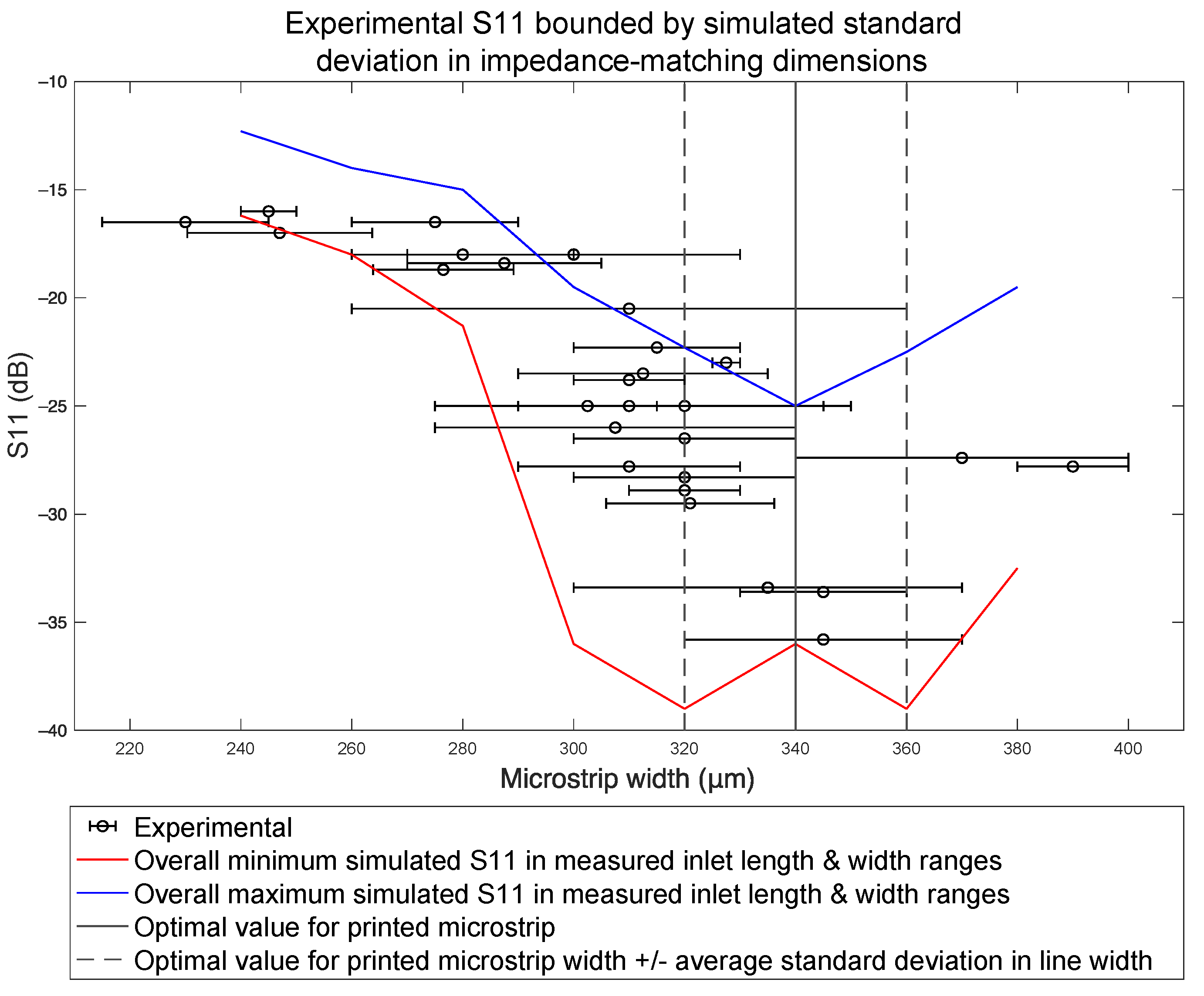
4.3. Combined Analysis

To combine the effects of Section 4.1 and Section 4.2, bounding lines were plotted using the minimum and maximum S11 values at each microstrip width for all inlet length and all inlet width combinations that lay within one experimental standard deviation of experimental averages. At each microstrip width, inlet length varied from 2.45 μm to 2.61 μm and the inlet width was varied from 140 μm to 200 μm. Upper and lower performance bounds and are shown in Figure 6 with the best-performing microstrip width of 340 μm marked by a black vertical line. The dashed vertical lines represent the average of the standard deviation in width along any microstrip in the whole experimental sample set.
While simulations demonstrate that resonance depths of up −35 dB can be achieved at the theoretically ideal microstrip width of 300 μm, variation in inlet width and length introduced by DW printing can significantly alter performance to as low as −14 dB. When analyzing a printed microstrip with an average width of 300 μm (50 Ω impedance), the actual performance falls across nearly the entire bounded region. However, Figure 6 shows that designing for a 340 μm wide microstrip (45.35 Ω impedance) offers a more consistent performance area and a deeper average resonance: −23 dB to −38 dB overall. Therefore, altering design with respect to the bounding effects of measured variability improves the lower-bound performance of the dataset by 9 dB, from −14 dB to −23 dB. It is true that variability in waveguide impedance changes the reflection coefficient at the SMA/microstrip interface (in this case a very small change of 0.038 at a width of 280 μm and 0.042 at a width of 320 μm), possibly reducing performance. However, a much greater impact can be seen from variability in capacitive coupling and the impedance matching effects between the microstrip and the patch antenna. The results demonstrate a need to design with respect to variability, and not the theoretical ideal. As such, at 340 μm wide the microstrip standard deviation would bound a performance region between −38dB to −23dB. Using a similar analytical process as detailed in Figure 7, it becomes possible to apply this knowledge to other printed antenna and waveguide combinations, other printing processes, and other systems with more or less variability. In all cases, the result will be a larger through-put of acceptable RF systems by creating larger region of acceptable processing parameters and conditions.

5. Conclusions

This work demonstrates that the primary mechanism for reduced RF antenna performance is through compounding variations in print dimensionality. Other common inconsistencies, such as surface roughness and sample height, are found to have little effect on performance when compared to dimensional variability. Although printing inconsistency is shown to affect the characteristic impedance of transmission lines, the primary driving mechanism for RF quality is determined to be the transmission line and antenna junction. Within this region, there are compounding effects due to correlated variability in multiple critical features. The resulting features demonstrate multiple, non-ideal dimensions, which can combine to create unpredictable RF devices. As such, this work has devised a method to design and predict RF performance by developing performance regions based on a characterized standard deviation of printed features. Specifically, this method utilizes the standard deviations of printed transmission line width in order to determine the range of antenna performance. This work analyzed a case study using a patch antenna and micropen dispensing system to increase minimum large-batch performance from −14 dB to −23 dB while maintaining a peak performance at −38 dB. The proposed process can easily be applied to a variety deposition systems and antenna designs, as well as expanded to encompass behavior among multiple antennas, such as rectangular, triangular, and hammer-shaped array configurations [49,50]. Additionally, this method could be used to develop training sets for ML algorithms aimed at determining optimal design values for RF structures based on measured system variability.
Finally, the overall process outlined in this work can be applied to all dielectric thicknesses and dielectric constants. In each case, the design process outlined in this work will not change. For example, increasing substrate thickness or decreasing dielectric constant will reduce the effect of process variability moving the design dimensions closer to the ideal dimensions. The applicability of this new design paradigm can be directly implemented to not only increase manufacturing yield, but also to push printed, flexible, and conformal RF manufacturing into a variety of new and exciting applications.

Author Contributions

Writing, formal analysis, investigation, methodology, K.B. and C.S.; Investigation, review and editing, E.M.B., B.P., S.F. and G.F.W.; Supervision, A.A., C.A., G.F.W., C.A. and C.S.; Funding acquisition, G.F.W. and C.S. All authors have read and agreed to the published version of the manuscript.

Funding

This research was funded by HEROES SLIMMER2 initiative and the DEVCOM Soldier Center, grants BAA W911QY-15-R-0016 and BAA W911QY-18-2-0006.

Institutional Review Board Statement

Not applicable.

Informed Consent Statement

Not applicable.

Data Availability Statement

The data presented in this study are available on request from the corresponding author.

Acknowledgments

All work was carried out at the Printed Electronics Research Collaborative (PERC) and the Raytheon UMass Lowell Research Institute (RURI). A special thanks is given to Edward Kingsley and John Lovaasen for their support in this project.

Conflicts of Interest

The authors declare no conflict of interest. The funders had no role in the design of the study; in the collection, analyses, or interpretation of data; in the writing of the manuscript, or in the decision to publish the results.

References

  1. Syafrindo, R.A.; Sumantyo, J.T.S.; Santosa, C.E.; Munir, A. 3D print X-band horn antenna for ground-based SAR application. In Proceedings of the 2017 Progress in Electromagnetics Research Symposium-Spring (PIERS), St Petersburg, Russia, 22–25 May 2017; pp. 1250–1253. [Google Scholar]
  2. Guo, C.; Shang, X.; Lancaster, M.J.; Xu, J. A 3-D printed lightweight X-band waveguide filter based on spherical resonators. IEEE Microw. Wirel. Compon. Lett. 2015, 25, 442–444. [Google Scholar] [CrossRef] [Green Version]
  3. Cai, F.; Khan, W.T.; Papapolymerou, J. A low loss X-band filter using 3-D polyjet technology. In Proceedings of the 2015 IEEE MTT-S International Microwave Symposium, Phoenix, AZ, USA, 17–22 May 2015; pp. 1–4. [Google Scholar]
  4. Zhao, Y.; Luo, J.; Lian, H.; Qi, L. 3D Printing of Micro Electrolyte Film by Using Micro-pen-writing. In Proceedings of the 2018 IEEE International Conference on Manipulation, Manufacturing and Measurement on the Nanoscale (3M-NANO), Hangzhou, China, 13–17 August 2018; pp. 249–252. [Google Scholar]
  5. Luo, J.; Zhao, Z.; Qi, L.; Lian, H.; Zhao, Y. Direct Fabrication of Micron-Thickness PVA-CNT Patterned Films by Integrating Micro-Pen Writing of PVA Films and Drop-on-Demand Printing of CNT Micropatterns. Nanomaterials 2021, 11, 2335. [Google Scholar] [CrossRef] [PubMed]
  6. Paulsen, J.A.; Renn, M.; Christenson, K.; Plourde, R. Printing conformal electronics on 3D structures with Aerosol Jet technology. In Proceedings of the 2012 Future of Instrumentation International Workshop (FIIW) Proceedings, Gatlinburg, TN, USA, 8–9 October 2012; pp. 1–4. [Google Scholar]
  7. Jordan, C.D.; Thorne, B.R.; Wadhwa, A.; Losey, A.D.; Ozhinsky, E.; Kondapavulur, S.; Hetts, S.W. Wireless resonant circuits printed using aerosol jet deposition for MRI catheter tracking. IEEE Trans. Biomed. Eng. 2019, 67, 876–882. [Google Scholar] [CrossRef] [PubMed]
  8. He, H.; Tajima, J.; Sydänheimo, L.; Nishikawa, H.; Ukkonen, L.; Virkki, J. Inkjet-printed antenna-electronics interconnections in passive UHF RFID tags. In Proceedings of the 2017 IEEE MTT-S International Microwave Symposium (IMS), Honololu, HI, USA, 4–9 June 2017; pp. 598–601. [Google Scholar]
  9. Tayyab, M.; Sharawi, M.S.; Shamim, A.; Al-Sarkhi, A. A low complexity RF based sensor array for lung disease detection using inkjet printing. Int. J. RF Microw. Comput.-Aided Eng. 2019, 29, e21586. [Google Scholar] [CrossRef]
  10. Shaker, G.; Safavi-Naeini, S.; Sangary, N.; Tentzeris, M.M. Inkjet printing of ultrawideband (UWB) antennas on paper-based substrates. IEEE Antennas Wirel. Propag. Lett. 2011, 10, 111–114. [Google Scholar] [CrossRef] [Green Version]
  11. Vaillancourt, J.; Zhang, H.; Vasinajindakaw, P.; Xia, H.; Lu, X.; Han, X.; Renn, M. All ink-jet-printed carbon nanotube thin-film transistor on a polyimide substrate with an ultrahigh operating frequency of over 5 GHz. Appl. Phys. Lett. 2008, 93, 444. [Google Scholar] [CrossRef] [Green Version]
  12. Trotter, M.; Juric, D.; Bagherian, Z.; Borst, N.; Gläser, K.; Meissner, T.; Zimmermann, A. Inkjet-printing of nanoparticle gold and silver ink on cyclic olefin copolymer for DNA-sensing applications. Sensors 2020, 20, 1333. [Google Scholar] [CrossRef] [Green Version]
  13. Njogu, P.M.; Sanz-Izquierdo, B.; Jun, S.Y.; Kalman, G.; Gao, S.; Malas, A.; Gibbons, G.J. Evaluation of planar inkjet-printed antennas on a low-cost origami flapping robot. IEEE Access 2020, 8, 164103–164113. [Google Scholar] [CrossRef]
  14. Lopes, A.J.; MacDonald, E.; Wicker, R.B. Integrating stereolithography and direct print technologies for 3D structural electronics fabrication. Rapid Prototyp. J. 2012, 18, 129–143. [Google Scholar] [CrossRef]
  15. Zips, S.; Wenzel, O.J.; Rinklin, P.; Grob, L.; Terkan, K.; Adly, N.Y.; Wolfrum, B. Direct stereolithographic 3D printing of microfluidic structures on polymer substrates for printed electronics. Adv. Mater. Technol. 2019, 4, 1800455. [Google Scholar] [CrossRef]
  16. Santoliquido, O.; Camerota, F.; Rosa, A.; Ortona, A. A novel device to simply 3D print bulk green ceramic components by stereolithography employing viscous slurries. Open Ceram. 2021, 5, 100089. [Google Scholar] [CrossRef]
  17. Shemelya, C.; Cedillos, F.; Aguilera, E.; Maestas, E.; Ramos, J.; Espalin, D.; MacDonald, E. 3D printed capacitive sensors. In Proceedings of the SENSORS, 2013 IEEE, Baltimore, MD, USA, 3–6 November 2013; pp. 1–4. [Google Scholar]
  18. Shemelya, C.M.; Zemba, M.; Liang, M.; Espalin, D.; Kief, C.; Xin, H.; MacDonald, E.W. 3D printing multi-functionality: Embedded RF antennas and components. In Proceedings of the 2015 9th European Conference on Antennas and Propagation (EuCAP), Lisbon, Portugal, 13–17 April 2015; pp. 1–5. [Google Scholar]
  19. Yu, X.; Liang, M.; Shemelya, C.; Roberson, D.A.; Wicker, R.; MacDonald, E.; Xin, H. 3-D printed parts for a multilayer phased array antenna system. IEEE Antennas Wirel. Propag. Lett. 2018, 17, 2150–2154. [Google Scholar] [CrossRef]
  20. Liang, M.; Shemelya, C.; MacDonald, E.; Wicker, R.; Xin, H. Fabrication of microwave patch antenna using additive manufacturing technique. In Proceedings of the 2014 USNC-URSI Radio Science Meeting (Joint with AP-S Symposium), Memphis, TN, USA, 6–11 July 2014; p. 269. [Google Scholar]
  21. Liang, M.; Yu, X.; Shemelya, C.; MacDonald, E.; Xin, H. 3D printed multilayer microstrip line structure with vertical transition toward integrated systems. In Proceedings of the 2015 IEEE MTT-S International Microwave Symposium, Phoenix, AZ, USA, 17–22 May 2015; pp. 1–4. [Google Scholar]
  22. Shemelya, C.; Cedillos, F.; Aguilera, E.; Espalin, D.; Muse, D.; Wicker, R.; MacDonald, E. Encapsulated copper wire and copper mesh capacitive sensing for 3-D printing applications. IEEE Sens. J. 2014, 15, 1280–1286. [Google Scholar] [CrossRef]
  23. Ning, F.; Cong, W.; Hu, Y.; Wang, H. Additive manufacturing of carbon fiber-reinforced plastic composites using fused deposition modeling: Effects of process parameters on tensile properties. J. Compos. Mater. 2017, 51, 451–462. [Google Scholar] [CrossRef]
  24. Wang, Y.; Kwok, H.Y.; Pan, W.; Zhang, Y.; Zhang, H.; Lu, X.; Leung, D.Y. Printing Al-air batteries on paper for powering disposable printed electronics. J. Power Sources 2020, 450, 227685. [Google Scholar] [CrossRef]
  25. Willert, A.; Baumann, R.R. Customized printed batteries driving sensor applications. In Proceedings of the 2013 International Semiconductor Conference Dresden-Grenoble (ISCDG), Dresden, Germany, 26–27 September 2013; pp. 1–4. [Google Scholar]
  26. Chason, M.; Brazis, P.W.; Zhang, J.; Kalyanasundaram, K.; Gamota, D.R. Printed organic semiconducting devices. Proc. IEEE 2005, 93, 1348–1356. [Google Scholar] [CrossRef]
  27. Unander, T.; Nilsson, H.E. Characterization of printed moisture sensors in packaging surveillance applications. IEEE Sens. J. 2009, 9, 922–928. [Google Scholar] [CrossRef]
  28. Nilsson, H.E.; Andersson, H.A.; Manuilskiy, A.; Unander, T.; Hammarling, K.; Siden, J.; Gulliksson, M. Printed write once and read many sensor memories in smart packaging applications. IEEE Sens. J. 2010, 11, 1759–1767. [Google Scholar] [CrossRef]
  29. Wu, T.; Gray, E.; Chen, B. A self-healing, adaptive and conductive polymer composite ink for 3D printing of gas sensors. J. Mater. Chem. C 2018, 6, 6200–6207. [Google Scholar] [CrossRef] [Green Version]
  30. Luo, Y.; Wu, D.; Zhao, Y.; Chen, Q.; Xie, Y.; Wang, M.; Sun, D. Direct write of a flexible high-sensitivity pressure sensor with fast response for electronic skins. Org. Electron. 2019, 67, 10–18. [Google Scholar] [CrossRef]
  31. Munasinghe, M.I.N.P.; Miles, L.; Paul, G. Direct-write fabrication of wear profiling IoT sensor for 3D printed industrial equipment. In Proceedings of the 36th International Symposium on Automation and Robotics in Construction, ISARC 2019, Banff, AB, Canada, 21–24 May 2019. [Google Scholar]
  32. Zheng, L.R.; Nejad, M.B.; Rodriguez, S.; Zhang, L.; Chen, C.; Tenhunen, H. System-on-flexible-substrates: Electronics for future smart-intelligent world. In Proceedings of the Conference on High Density Microsystem Design and Packaging and Component Failure Analysis, 2006. HDP’06. Shanghai, China, 27–28 June 2006; pp. 29–36. [Google Scholar]
  33. Hoey, J.M.; Reich, M.T.; Halvorsen, A.; Vaselaar, D.; Braaten, K.; Maassel, M.; Schulz, D.L. Rapid prototyping RFID antennas using direct-write. IEEE Trans. Adv. Packag. 2009, 32, 809–815. [Google Scholar] [CrossRef]
  34. Anagnostou, D.E.; Gheethan, A.A.; Amert, A.K.; Whites, K.W. A direct-write printed antenna on paper-based organic substrate for flexible displays and WLAN applications. J. Disp. Technol. 2010, 6, 558–564. [Google Scholar] [CrossRef]
  35. Lee, H.; Tentzeris, M.M.; Markondeya, P.; Raj, M.K.; Kawahara, Y. Inkjet-printed ferromagnetic nanoparticles for miniaturization of flexible printed RF inductors. In Proceedings of the 2013 IEEE Antennas and Propagation Society International Symposium (APSURSI), Orlando, FL, USA, 7–13 July 2013; pp. 994–995. [Google Scholar]
  36. McKerricher, G.; Perez, J.G.; Shamim, A. Fully inkjet printed RF inductors and capacitors using polymer dielectric and silver conductive ink with through vias. IEEE Trans. Electron Devices 2015, 62, 1002–1009. [Google Scholar] [CrossRef]
  37. George, J.; Abdelghani, A.; Bahoumina, P.; Tantot, O.; Baillargeat, D.; Frigui, K.; Dejous, C. CNT-based inkjet-printed RF gas sensor: Modification of substrate properties during the fabrication process. Sensors 2019, 19, 1768. [Google Scholar] [CrossRef] [Green Version]
  38. Lis, M.; Plaut, M.; Zai, A.; Cipolle, D.; Russo, J.; Lewis, J.; Fedynyshyn, T. Polymer Dielectrics for 3D-Printed RF Devices in the Ka Band. Adv. Mater. Technol. 2016, 1, 1600027. [Google Scholar] [CrossRef]
  39. Bito, J.; Palazzi, V.; Hester, J.; Bahr, R.; Alimenti, F.; Mezzanotte, P.; Tentzeris, M.M. Millimeter-wave ink-jet printed RF energy harvester for next generation flexible electronics. In Proceedings of the 2017 IEEE Wireless Power Transfer Conference (WPTC), Taipei, Taiwan, 10–12 May 2017; pp. 1–4. [Google Scholar]
  40. Pham, D.T.; Subbaraman, H.; Chen, M.Y.; Xu, X.; Chen, R.T. Light Weight and Conformal 2-Bit, 1x4 Phased-Array Antenna With CNT-TFT-Based Phase Shifter on a Flexible Substrate. IEEE Trans. Antennas Propag. 2011, 59, 4553–4558. [Google Scholar] [CrossRef]
  41. Kimionis, J.; Georgiadis, A.; Isakov, M.; Qi, H.J.; Tentzeris, M.M. 3D/inkjet-printed origami antennas for multi-direction RF harvesting. In Proceedings of the 2015 IEEE MTT-S International Microwave Symposium, Phoenix, AZ, USA, 17–22 May 2015; pp. 1–4. [Google Scholar]
  42. Sarsen, A.; Valagiannopoulos, C. Robust polarization twist by pairs of multilayers with tilted optical axes. Phys. Rev. B 2019, 99, 115304. [Google Scholar] [CrossRef]
  43. Lu, Y.; Subramani, K.S.; Huang, H.; Kupp, N.; Huang, K.; Makris, Y. A comparative study of one-shot statistical calibration methods for analog/RF ICs. In Proceedings of the 2015 IEEE International Test Conference (ITC), Anaheim, CA, USA, 6–8 October 2015; pp. 1–10. [Google Scholar]
  44. Zhumabek, T.; Valagiannopoulos, C. Light trapping by arbitrarily thin cavities. Phys. Rev. Res. 2020, 2, 043349. [Google Scholar] [CrossRef]
  45. Fu, Z.; Angeline, V.; Sun, W. Evaluation of Printing Parameters on 3D Extrusion Printing of Pluronic Hydrogels and Machine Learning Guided Parameter Recommendation. Int. J. Bioprinting 2021, 7, 434. [Google Scholar] [CrossRef]
  46. Shi, J.; Song, J.; Song, B.; Lu, W.F. Multi-objective optimization design through machine learning for drop-on-demand bioprinting. Engineering 2019, 5, 586–593. [Google Scholar] [CrossRef]
  47. Shirsavar, M.A.; Taghavimehr, M.; Ouedraogo, L.J.; Javaheripi, M.; Hashemi, N.N.; Koushanfar, F.; Montazami, R. Machine Learning-Assisted E-jet Printing of Organic Flexible Biosensors. arXiv 2021, arXiv:2111.03985. [Google Scholar]
  48. Huang, H.J.; Zhou, M.B.; Yin, C.; Chen, Q.W.; Zhang, X.P. Preparation of a low temperature sintering silver nanoparticle ink and fabrication of conductive patterns on PET substrate. In Proceedings of the 2018 19th International Conference on Electronic Packaging Technology (ICEPT), Shanghai, China, 8–11 August 2018; pp. 482–485. [Google Scholar]
  49. Sharma, V.; Upadhayay, M.D.; Singh, A.V.; Prajapati, J. Hammer-Shaped Element-Based Compact MIMO Antenna for WLAN Application. Prog. Electromagn. Res. Lett. 2021, 97, 121–130. [Google Scholar] [CrossRef]
  50. Khraisat, Y.S.; Olaimat, M.M. Comparison between rectangular and triangular patch antennas array. In Proceedings of the 2012 19th International Conference on Telecommunications (ICT), Jounieh, Lebanon, 23–25 April 2012; pp. 1–5. [Google Scholar]
Figure 1. Feature measurement: (a) Graph showing the x-profile of an antenna along the dashed line of the profilometer image, with black and white triangular indicators marking the point of 3 μm height (skin depth) on either side of the microstrip. Δ X   measures the space between the markers and is taken as the microstrip width: 321 μm for this cross-section; (b) Plot showing average surface roughness compared with respective antenna S11 response at 8 GHz. Surface roughness was measured as Sq, or root mean square height, on the antenna patch using the same profilometry software as in (a). We expect no change to the trends calculated in this work if we instead used arithmetical mean roughness Ra. Results in (b) show no noticeable correlation between roughness and S11 in this dataset.
Designs 06 00013 g001
Figure 2. Antenna S11 response plotted by variation in the average value of single features: (a) Fully printed antenna with measured dimensions called out; (b) Microstrip width vs. S11 for each antenna in the dataset; (c) Impedance matching inlet width vs. S11; (d) Impedance matching inlet length vs. S11. Error bars represent the standard deviation from the average plotted value for the x-axis feature in each antenna. Solid lines in (c,d) illustrate simulation sweeps across the x-axis values, holding all other features constant at the dataset average. These simulations are discussed in Section 4.2 and Section 4.3.
Designs 06 00013 g002
Figure 3. S21 transmission values for a range of microstrip widths across the 8 GHz frequency of interest show no significant change as microstrip width increases. This data suggests that the trend towards a more negative S11 with increasing microstrip width, Figure 2b, is not caused solely by the microstrip variability.
Designs 06 00013 g003
Figure 4. Simulated performance across the average +/− standard deviation of inlet width at each microstrip width forming ranges of RF performance. The bounds illustrate the capacitive coupling effects (inlet width) on S11, but do not enable full predictive performance metrics.
Designs 06 00013 g004
Figure 5. Simulated performance across the average +/−standard deviation of inlet length at each microstrip width forming ranges of RF performance. The bounds follow a similar trend as the inlet width dictated bounds (Figure 4), but do not form a fully predictive model.
Designs 06 00013 g005
Figure 6. Experimental data bounded by simulation models including variation of both printed inlet length and inlet width. These bounds encapsulate the S11 results that can be expected given the level of variation in the impedance matching inlet dimensions. The average standard deviation of 20 μm in printed microstrip width along any given microstrip is depicted by the dashed lines. The figure demonstrates that a microstrip designed at 340 μm will produce a more consistent antenna design given experimentally determined print variability.
Designs 06 00013 g006
Figure 7. Flowchart depicting process of measuring inherent variation in a given printing system and using these constraints to adapt RF component design dimensions to select the ideal set of values for highest manufacturing yield of high-performing units.
Designs 06 00013 g007
Publisher’s Note: MDPI stays neutral with regard to jurisdictional claims in published maps and institutional affiliations.

