1. Introduction
The electrification of the powertrain is a promising solution for a sustainable and environmentally friendly transport system [
1]. Furthermore, electromobility represents an essential contribution to climate protection and renewable energies in the transport sector [
2]. For this reason, automobile manufacturers are increasingly offering battery electric vehicles (BEVs). In the electric architecture of BEVs, the battery is the only energy source for the electric drive; its operating voltage is typically below the DC bus to which the traction inverter is connected. Thus, a bidirectional buck–boost converter connects the battery to the DC bus. Furthermore, fuel-cell-based electromobility will also contribute to an environmentally friendly transport system. Studies indicate that 17% of the annually sold vehicles will be fuel-cell-based starting in 2050 [
3]—for example, the fuel cell hybrid vehicle (FCHV). FCHVs use a battery as a second energy source in addition to the fuel cell, providing peak power for dynamic load reduction on the fuel cell system [
4,
5]. This battery support is essential during acceleration and cold starts.
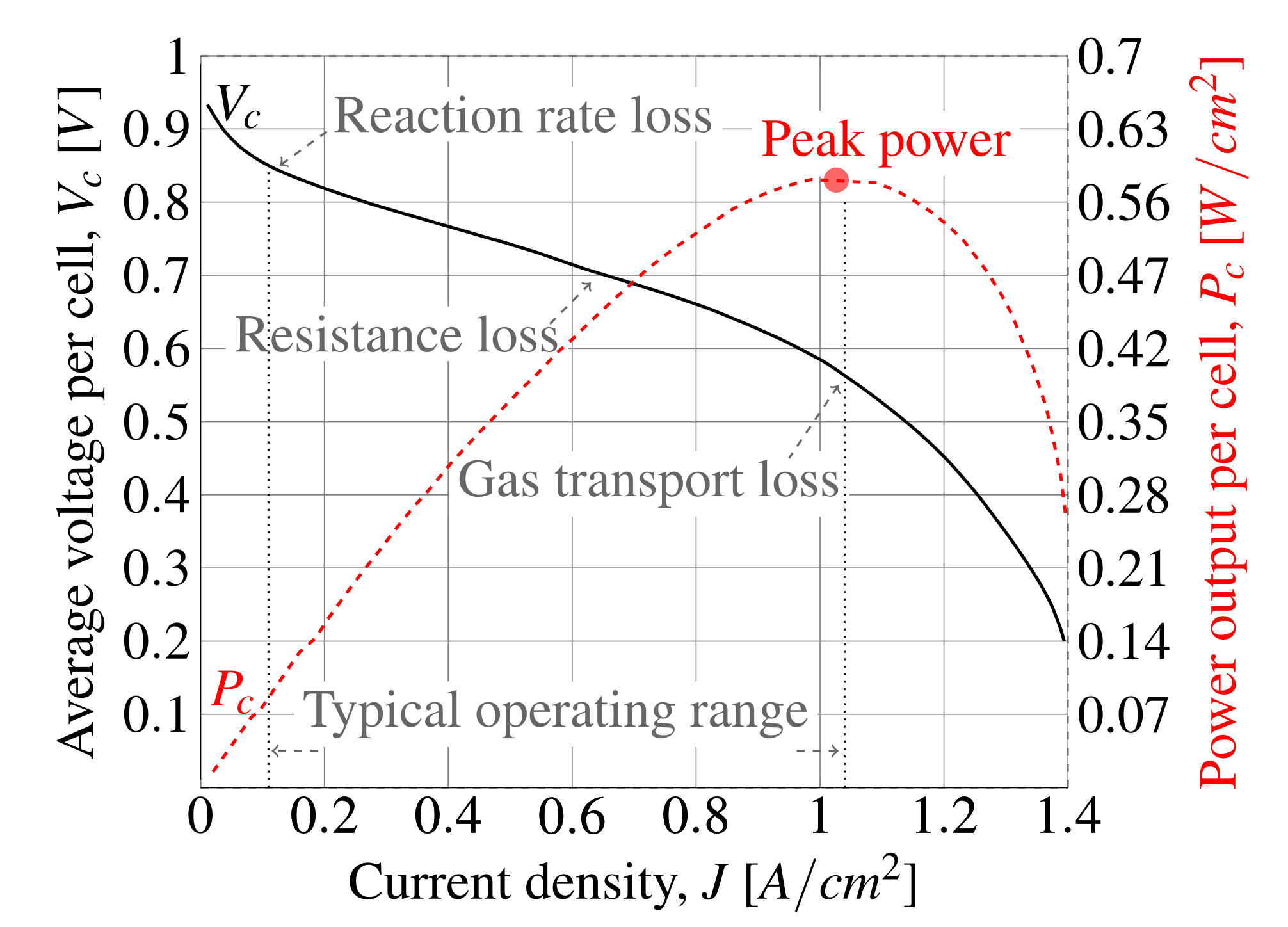
Figure 1 shows the polarization curve of a proton-exchange membrane fuel cell (PEMFC) with its losses typically used in automotive applications. The cell voltage is load-dependent due to the reaction rate loss, resistance loss, and gas transport loss.
Two electric architectures in FCHVs are of interest for future applications.
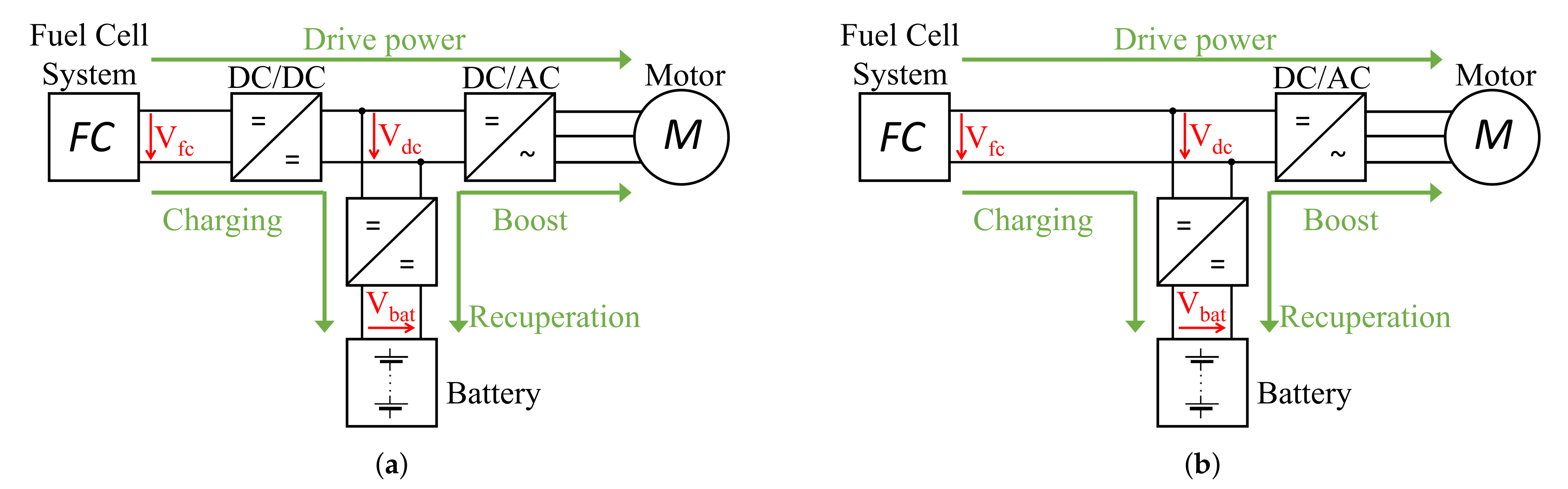
Figure 2a illustrates the system in which a boost converter connects the fuel cell to the DC bus [
5,
7]. The motor interfaces the DC bus via a bidirectional DC–AC converter. In addition, this architecture uses a bidirectional buck–boost converter in front of the battery.
Figure 2b illustrates an alternative solution, where the output terminals of the fuel cell are connected directly to the DC bus [
5,
7]. However, depending on the state of charge of the battery and the load-dependent fuel cell voltage (see the typical operating range in
Figure 1), both voltage levels can overlap. For this reason, a bidirectional DC–DC converter is necessary, interfacing both voltage characteristics to enable good cold-start behaviour, flexible power control, regenerative braking, and to avoid dynamic current stress of the fuel cell stack by providing additional traction power during acceleration [
8,
9,
10]. For these reasons, optimising the bidirectional DC–DC converters in front of the battery is essential for vehicle performance. Basically, three topologies are suitable, the bidirectional CúK, SEPIC/ZETA, and cascaded buck and boost converter. Nevertheless, a previous study [
11] demonstrates that in terms of electric stress on the power semiconductors and converter volume, the cascaded buck and boost converter is an appropriate topology for FCHVs to interface the battery to the DC bus. For example, the study in [
11] demonstrates that the cascaded buck and boost converter topology reduces the required inductance to a fifth and the capacitance value by ∼5% compared to the CúK and SEPIC/ZETA converter. As the inductance relates to the energy-handling capability and, therefore, the volume of the inductor, it indicates that the cascaded buck and boost converter decreases the converter volume for the application of interest accordingly. As the inductor of a DC–DC converter is a major contributor to the overall volume, the bidirectional cascaded buck and boost converter is thus a suitable topology for mobile applications such the FCHVs.
The published literature introduces two modulation modes for overlapping input and output voltages with the bidirectional cascaded buck and boost converter: the buck–boost and buck + boost modes. The subsequent section will quantify these modulation methods in detail. However, to summarise, the buck–boost mode uses four switches; in contrast, the buck + boost mode only uses two. Furthermore, the buck + boost mode operates with two duty cycles. One of these duty cycles needs to be constant. However, the literature does not determine the optimum for this constant duty cycle in terms of converter losses. Moreover, the literature does not sufficiently discuss the optimisation of the operation mode with overlapping input and output voltages. Instead, authors frequently introduce soft-switching concepts for efficiency improvement [
12]. However, the efficiency improvement does not justify the increase in converter volume due to the additional snubber circuits.
Further, the literature often refers to lower power applications (less than 10 kW) regarding the operation mode for overlapping input and output voltages, where authors often recommend the buck–boost mode [
13]. However, disregarding converter volume, which depends on the design process, application and other requirements, it is evident that the buck–boost mode would considerably reduce efficiency over the entire power range. Moreover, in the buck–boost mode, the inductor current is composed of the sum of converter input and output currents that would significantly increase magnetic core volume, especially in the mid-kW range (10 kW–50 kW).
For example, the low efficiency of the buck–boost mode is also demonstrated in [
12]. The study in [
12] introduces a buck–boost + LLC cascaded 1.12 kW converter using the dual-frequency PEM method. Furthermore, the authors investigate zero voltage switching (ZVS) and zero current switching (ZCS). Nonetheless, they achieve efficiencies of around 92% for the buck–boost mode. The study results in [
14] confirm this statement. The 100 W bidirectional cascaded buck and boost converter in [
14] does not exceed an efficiency of 95% at any operation point. Furthermore, the authors demonstrate efficiency improvement with GaN power semiconductors compared to Si power semiconductors using soft switching. However, the converter achieves a low power density of 0.5 kW/L, using a switching frequency of 10 MHz. In addition, the authors do not investigate the operation for overlapping input and output voltages. In addition, Ref. [
13] mentions the buck–boost mode’s disadvantages: high current ripples on the inductor and poor converter efficiency. The paper presents a hybrid buck–boost feedforward control method for a maximum power of 2.25 kW. Another example of low converter efficiency is [
15]. The converter only achieves an efficiency of 93%. The authors focused on buck- and boost mode transition for a 120 W bidirectional cascaded buck and boost converter.
This article will prove that using hard switching devices in buck + boost mode and the optimum fixed duty cycle and a simple modulation method can decrease power losses by up to 39% for overlapping input and output voltages. Unlike in [
12] or [
15], the results will prove soft-switching is unnecessary for optimisation. Furthermore, in contrast to [
14], this article will prove that optimising converter efficiency with Si-IGBTs half-bridge modules is possible. Finally, the suggested approach eliminates the drawback of [
13] of high computational effort and high current ripples due to its simplicity.
A method for efficiency optimisation is switching frequency modulation, for example, by increasing the switching frequency to operate in critical conduction mode (CrCM). The CrCM is the boundary limit between continuous conduction mode (CCM) and discontinuous conduction mode (DCM). Another approach is to adjust the switching frequency until reaching the efficiency maximum depending on the operating point. Generally, a DC–DC converter has two main power loss contributors: the power semiconductors and the inductor. By increasing the switching frequency, the switching losses of the power semiconductor will rise. However, losses of the inductor will decrease as higher switching frequencies reduce the current ripple and the AC flux density. Therefore, a critical requirement for switching frequency modulation is the percentage power distribution of the DC–DC converter. Authors in published literature introduce CrCM approaches for DC–DC converters in the power range below 10 kW. However, for such low power ranges, the power losses of the power semiconductors approximately match the power losses of the DC inductor.
An example for this modulation method would be the study according to [
16] in which the authors operate the buck–boost mode with a fixed switching (FSF) frequency (20 kHz) and with switching frequency modulation (20 kHz–100 kHz) in CrCM. The results demonstrate poor efficiencies below 95% for
(light-load operation). The reason for this efficiency is that the converter operates with high switching frequencies in light-load to avoid DCM. Another study presents an algorithm for the control unit to adjust the switching frequency according to a calculated loss minimum depending on the output power [
17]. However, this approach has a high computational effort as the algorithm calculates the switching frequency according to power loss models with eight equations and several dynamic parameters. Moreover, the study does not investigate the operation mode with overlapping input and output voltages. The authors of the paper [
18] also investigate switching frequency modulation to enhance efficiency. The proposed approach consists of an algorithm that adjusts the switching frequency according to power loss measurements. However, such power measurements result in computational effort. In addition, the converter does not avoid DCM and operates with a maximum output power of 3.6 W.
References [
19,
20] analyse converters for power factor correction in CrCM. The results of these studies demonstrate a significant reduction in turn-on switching losses of the power semiconductors; however, the total switching losses increases. As shown in [
19,
20], the control unit requires high switching frequencies to avoid DCM. Indeed, the converter topologies for power factor correction are irrelevant for the application of this article. Nevertheless, the results prove the potential due to the turn-on of the transistors at the boundary limit of 0 A. A similar approach is shown in [
21] where the authors propose a CrCM control method for a boost converter. With additional hardware, the approach enables current-mirroring sensing with GaN transistors. The setup triggers the turn-on of the transistors as soon as reaching the boundary limit. Operating at the boundary limit, hence in CrCM, also reduces reverse recovery losses of diodes, which is confirmed by [
22]. In [
22], the authors propose a control method that increases switching frequency for CrCM, similar to [
19,
20]. Consequently, the results of [
22] show that increasing the switching frequency in light-load for CrCM causes electromagnetic interference (EMI). Therefore, the authors in [
22] propose an approach to reduce input current harmonic values for a 120 W prototype converter. The reason for EMI in CrCM in [
22] is the high switching frequency to avoid DCM. In [
22], the switching frequency in light-load is higher than in full-load by a factor of five. As a result, the approach achieves low efficiencies. A study comparable to this article is [
16], where the authors analyse different control methods for the bidirectional cascaded buck and boost converter for hybrid electric vehicles and up to 30 kW in a simulation environment. However, by operating with CrCM, the converter in [
16] achieves a maximum converter efficiency of approximately 97%.
This study aims to improve the efficiency of the bidirectional cascaded buck and boost converter for operation with overlapping input and output voltages using the buck + boost mode. For this reason, this paper investigates the resulting problem of high current ripples and the impact of the fixed duty cycle on converter losses. This article introduces a novel load-dependent switching frequency modulation for efficiency optimisation, namely the critical conduction mode with adapted switching frequency (CrCMASF). The investigation exemplifies that the introduced modulation method ensures CCM using powder cores and the soft saturation characteristic. The findings are validated by measurements on an experimental setup and reveal that the proposed duty cycle and modulation method enable converter efficiencies of up to 99%. Furthermore, measurements demonstrate that the introduced approach decreases the junction temperature of the power semiconductors significantly. The results of this article will prove that the suggested approach will decrease computational effort considerably compared to [
17] or [
18]. The novel method will only use one equation with one dynamic parameter, which is the current-dependent inductance of the inductor. Furthermore, no additional hardware is necessary compared to [
21]. In addition, in contrast to [
22], the proposed method will decrease switching frequency in light-load. Therefore, this paper will demonstrate that by CrCMASF, EMI will not deteriorate. Finally, compared to [
16,
23], the proposed modulation method enables high efficiencies for the entire power range. Further discoveries on this literature review will be presented on
Section 6 subject to the findings of this research.
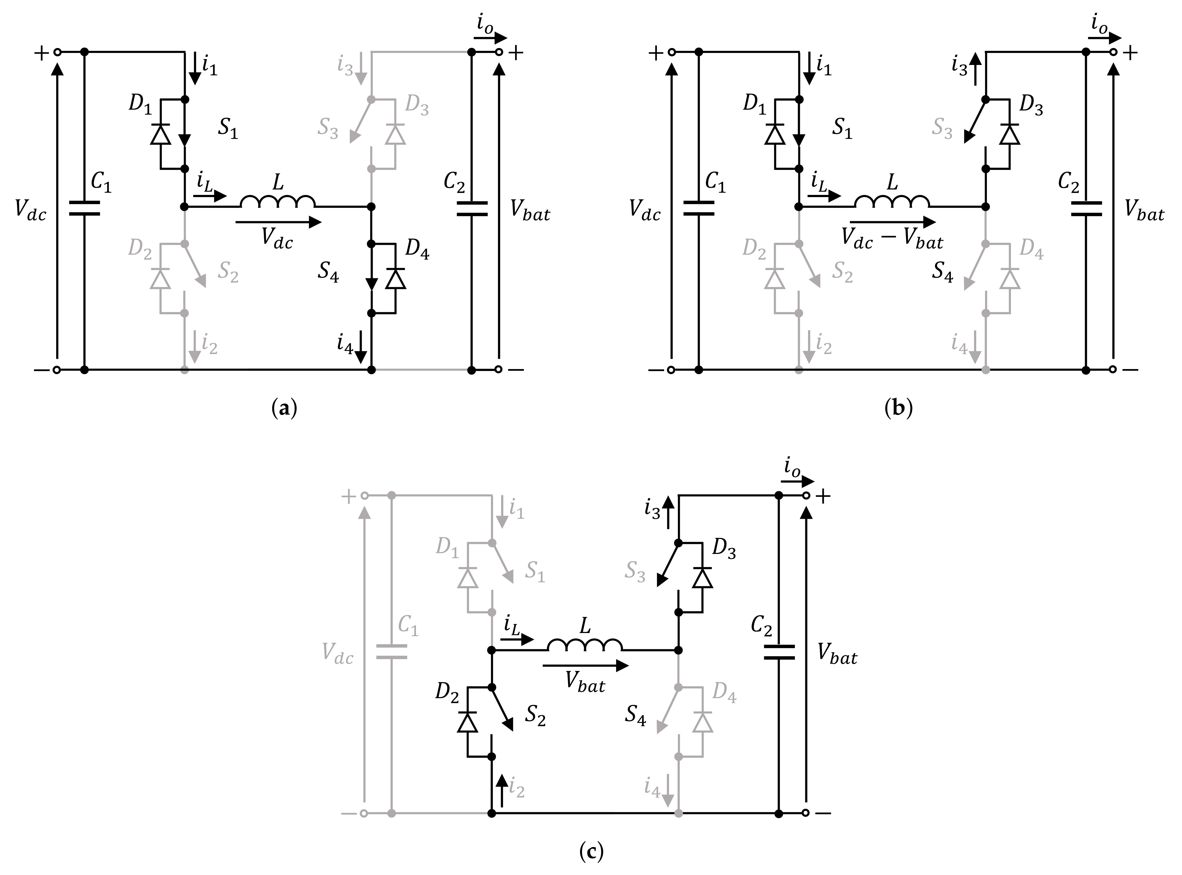
2. PWM Control Methods
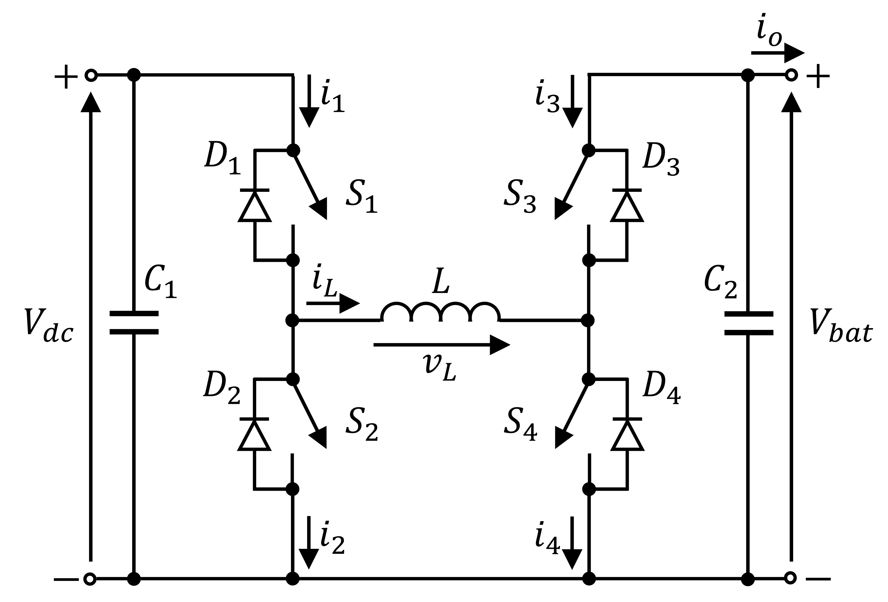
Figure 3 depicts the non-isolated hard-switched bidirectional cascaded buck and boost converter (hereinafter referred to as converter). This converter is the anti-parallel combination of a buck and boost converter (half-bridge) with a connected second-order low-pass filter. The half-bridge configuration enables the current to flow in both directions with positive input and output voltages using anti-parallel diodes. According to the circuit in
Figure 3, the converter operates in buck mode by controlling
or
and in boost mode by controlling
or
. The diodes
,
,
, and
act as freewheeling diodes accordingly. The converter allows the output voltage to be higher, lower, or equal to the input voltage.
Table 1 summarises the control of the transistors to operate in the respective mode. The converter can operate in buck, boost, buck–boost, or buck + boost mode; power flow from the DC bus to the battery or vice versa is possible for all operation modes. For convenience, this study assumes a power flow from the DC bus to the battery for further discussion. The following section analyses the operation mode with overlapping input and output voltages (
≈
). The literature introduces two options for power transfer.
Figure 4 illustrates the current
through inductance
L for switches
to
for the first method. In this method, called buck–boost, switches
and
are switched simultaneously with a duty cycle
, while switches
and
are switched simultaneously with a duty cycle
.
Figure 4 indicates that this method ensures that the average value of the inductor current
is composed of the sum of the converter currents
,
and
,
, which represent the input and output currents of the converter [
23]. This property is a disadvantage as the cores of the inductor with the inductance
L would need a high DC bias compatibility, especially in the high power range and for applications such as FCHVs where high currents are possible. As a result, the volume would increase considerably [
5].
Moreover, to ensure that the inductor voltage
on its average is zero, the duty cycles
and
must be 0.5 for equal voltages on the input and output. Furthermore, current peaks may occur. Admittedly, state-of-the-art controllers prevent the inductor current from increasing to unreasonable values. However, no controller can hold the current dynamically, which can lead to high current peaks. For example, a previous study investigated methods adapted for the control of the converter [
7], where the difficulty is evident in preventing unacceptably control deviation of the inductor current
during the transitions between buck mode and boost mode for overlapping input and output voltages.
Moreover, for the buck–boost mode, the approximately matching duty cycles cause high current ripples
, which increase the current stress on the switches, as shown in
Figure 4. The current stress results in considerable losses in the inductor and all switches.
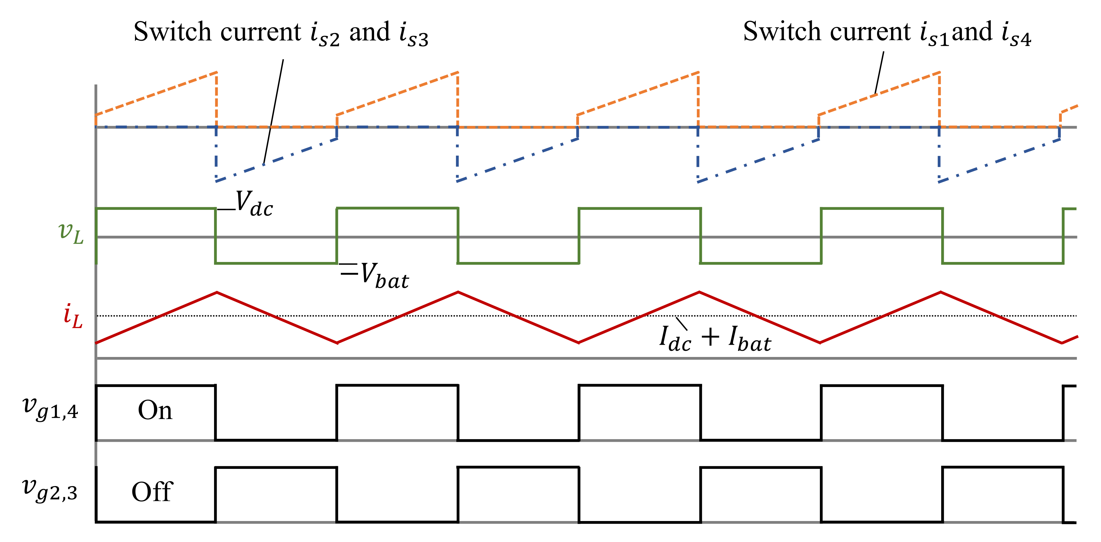
The buck + boost mode in
Figure 5 eliminates these drawbacks as it only uses two switches, switch
and switch
. One half of the converter in
Figure 3 operates as a buck converter, the other half as a boost converter. Thus, for switch
, a fixed duty cycle
is specified for buck mode, while switch
uses a variable duty cycle
in boost mode. It can be seen in
Figure 5 that by using one half of the topology as a buck and the other half as a boost converter, the inductor is energised and de-energised simultaneously after the rise time of the inductor current
. The average inductor current equals the output current, in this case, the battery current
. Because of the characteristic of inductor voltage
, the buck + boost mode can significantly reduce the current ripple
compared to the buck–boost mode [
24]. Thus, for buck + boost mode, if the duty cycle
of switch
is assumed to be constant, the duty cycle
for switch
is according to Equation (
1) with the input voltage
and output voltage
:
However, the question of how exactly the fixed duty cycle
with an appropriate transition should be determined remains. Reference [
25] confirms this statement as the literature to date does not address this topic adequately with regard to converter efficiency, and there is no appropriate investigation regarding the optimum fixed duty cycle
[
26,
27,
28]. The duty cycle
for switch
depends on the hysteresis, the range at which the converter should operate in buck and boost mode. This range is necessary to ensure a smooth transition between the operation modes and considers the voltage ripple on the DC bus, as shown in
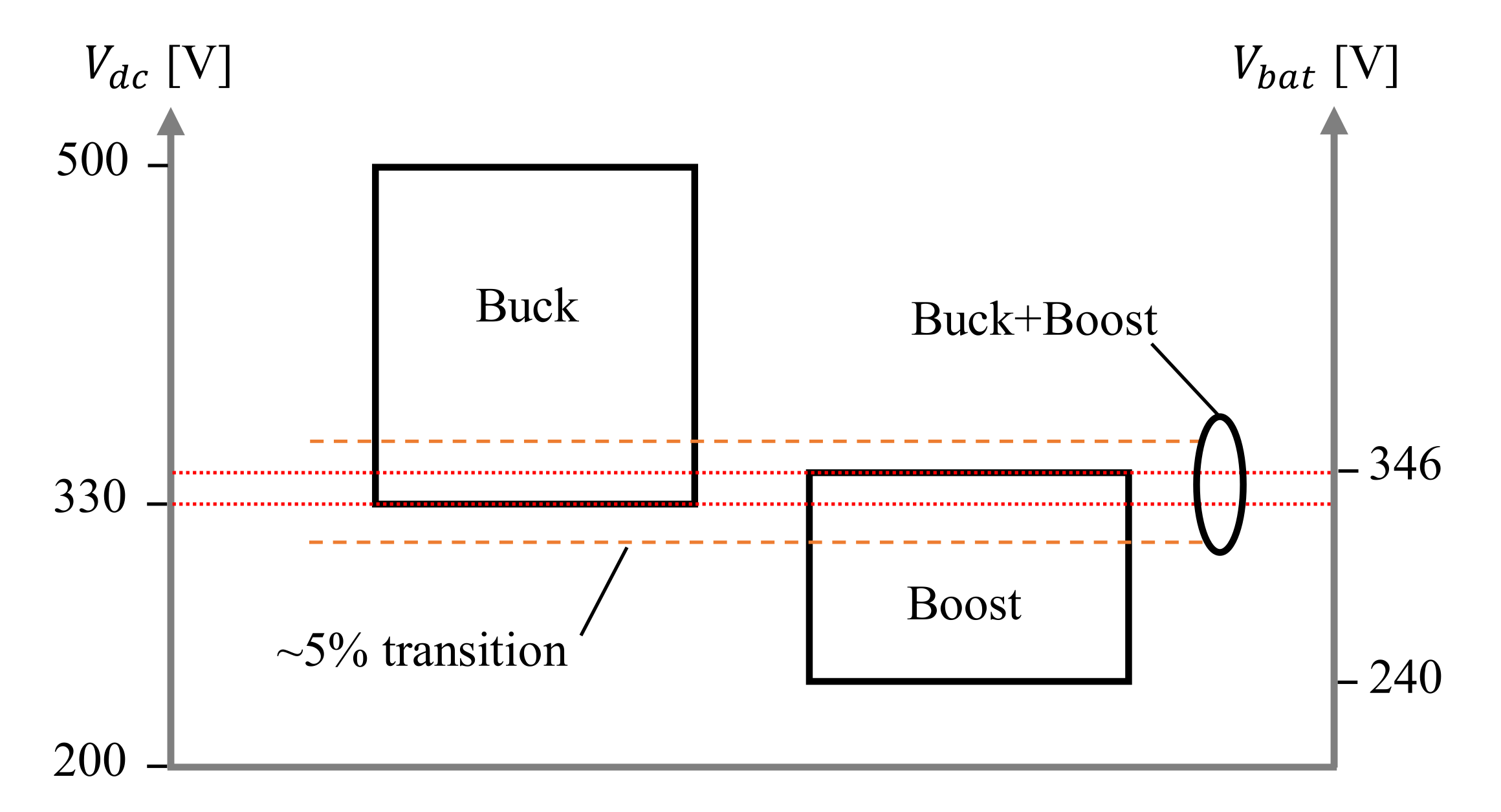
Figure 6 with a transition of 5%. Voltage ripples on the DC bus are typically around 10% of the DC component [
29]. Therefore, it is reasonable to assume a reduction of the input voltage for the buck part with a duty cycle between 0.8 and 0.95, with sufficient input and output capacitance for voltage stabilisation.
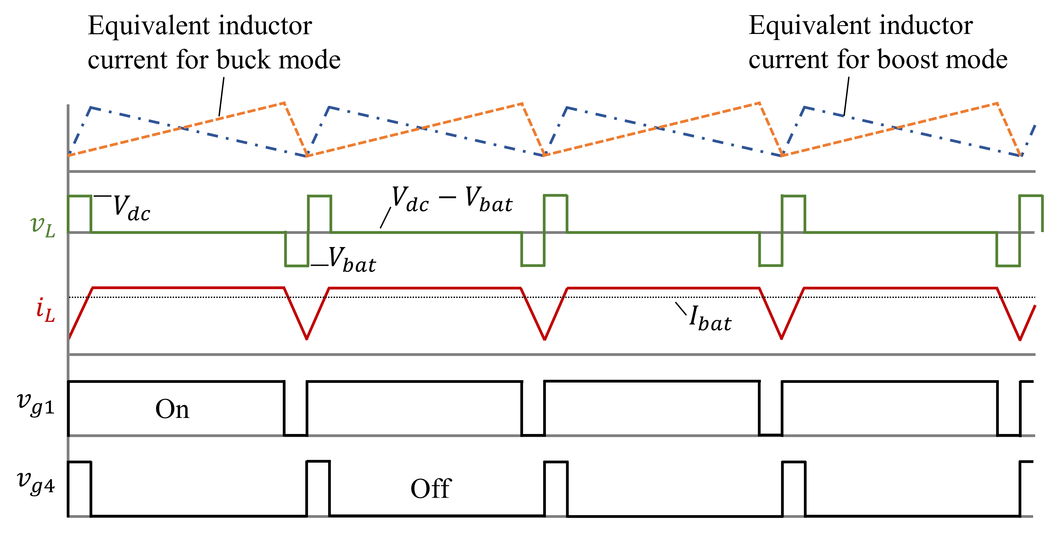
Figure 4 and
Figure 5 illustrate the voltage–time areas of the inductor. The maximum current ripple
in a period
always occurs for the state with the highest voltage level on the inductor. The buck + boost mode is analysed further in the following discussion with
Figure 5 and
Figure 7. As mentioned before, the power flow for this study is from the DC bus to the battery.
Figure 7a illustrates the first state, where the inductor voltage equals the DC bus voltage (
).
Figure 7b is the second state, where the inductor voltage is the difference between input and output voltages (
), and
Figure 7c is the last state, where the inductor voltage equals the battery voltage (
). In order to calculate the current ripple, state two is irrelevant as the voltage on the inductor cannot exceed the voltage level of input or output. Therefore, if the DC bus voltage is higher or equal to the battery voltage (
), it is possible to calculate the current ripple with the law of induction and
Figure 7a with the current dependent inductance
of the powder cores, and period
of the first state:
This first state energises the inductor for the period
according to
Figure 5 and
Figure 7a. The switching frequency is defined as
. Therefore, the current ripple is:
To calculate the current ripple for
, the characteristics illustrated in
Figure 7c define the voltage on the inductor. Using the law of induction for the third stage during time period
, the current ripple is:
In the third state, the period equals the off time of switch
, which is
. Therefore, by transforming Equation (
1) for
and substitution, the current ripple is:
Equations (
3) and (
5) are valid for both buck–boost and buck + boost mode. From Equation (
5), it is evident that for the buck–boost mode, the current ripple
is way higher for equal input and output voltages, as both duty cycles are 0.5.
The experimental setup uses parameters for validation according to the investigation in [
30]. The authors in [
30] assume an electric vehicle with approximately one-ton mass and a maximum DC bus current of 480 A. Generally, the maximum motor power in FCHVs is supplied 70% by the fuel cell stack and 30% by the battery [
24]. The study in [
30] uses a DC bus voltage of 300 V and a maximum power of 144 kW. Increasing the DC bus voltage (e.g., 500 V) decreases the maximum current. Therefore, according to the data of the FCHVs Hyundai Nexo and Honda Clarity Fuel Cell and the results of [
30], this article uses the following parameters for the experimental setup:
Maximum converter power in buck + boost mode, kW;
DC bus voltage range, V;
Battery voltage range, V;
Maximum converter current in buck + boost mode, A;
Maximum current ripple, A;
Input and output capacitance, F;
Inductance, H.
4. Critical Conduction Mode with Adapted Switching Frequency (CrCMASF)
A common method to decrease converter losses is to adjust the switching frequency
depending on the load. DC–DC converters include DC inductors designed for a specified maximum current ripple
. Authors in the published literature adjust the switching frequency depending on the load until reaching efficiency maximum, as shown in [
31]. However, in the mid-kW range, realising switching frequency modulation is challenging since the inductor usually consists of ferrite cores with low saturation flux densities (0.3–0.4 T) with almost constant inductance over the entire power range [
32,
33]. So far, no research has been published for the converter topology shown in
Figure 3 in the relevant power range with respect to the application of switching frequency modulation for the buck + boost mode.
Semiconductor switching losses dominate converter losses for the power range of interest using Si-IGBTs. For this reason, it is necessary to reduce the switching frequency to improve efficiency. However, at low switching frequencies, the current ripple
increases significantly, which in turn causes the AC flux density to rise, resulting in high losses on the magnetic cores. Consequently, the risk of reaching saturation is high. Moreover, the DC–DC converter could reach the DCM, and in terms of controller design, DCM should always be avoided. Solving these issues is possible by using powder cores with soft saturation characteristics and high saturation flux densities (0.5–1.5 T) [
32,
33]. The dependence of the powder cores inductance on the output current is due to the DC magnetising force-dependent permeability [
34].
The following section presents a simple way to estimate power losses. The aim is to illustrate the power loss distribution of the components. The main power loss contributors are the half-bridge modules, inductor, and output capacitors. Due to the limitations of the experimental setup, the validation refers to total converter losses. Furthermore, the estimations assume a junction temperature of approximately 50 °C as the experimental setup cannot measure junction temperatures of all IGBTs and diodes.
A simple way to estimate the losses of half-bridge modules is to use the loss characteristics from the datasheet. Compared to mathematical–analytical models, which can predict the switching behaviour accurately, this method has less effort without data acquisition, for example, the parasitic inductances and the transient turn-on and turn-off characteristics.
The power losses of Si-IGBT half-bridge modules are divided into conduction and switching losses. The losses occur during the power flow from the DC bus to the battery on switch
(
), switch
(
), diode
(
), and diode
(
). Therefore, the total average power loss of both Si-IGBT half-bridge modules
is:
In Equation (
6) the power losses of the IGBTs (
and
) are composed of switching losses (
and
) and conduction losses (
and
) and diode losses of reverse recovery losses (
and
) and forward conduction losses (
and
). Estimating the conduction losses of IGBTs
and diodes
is possible with the forward characteristic. The conduction losses of each IGBT for a periodic collector current
, and on-state resistance
is:
The calculation of Equation (
7) is possible with the definition of the on-state voltage
using the threshold voltage
of the IGBTs; the calculation for the conduction losses of the diodes is possible with the same procedure:
The diode and IGBT’s threshold voltage and on-state resistance are temperature-dependent and determined according to the output characteristics, and the on-state parameters from the datasheet [
35].
Switching losses of Si-IGBT half-bridge modules are the major contributor to converter losses in the specified power range. Accordingly, the converter losses depend on the switching frequency. The switching losses occur during the transient turn-on and turn-off process, where the current trough and voltage on the IGBT lead to power losses. The reverse recovery losses of the diodes occur during their turn-off due to the reverse current and voltage. Accordingly, the estimation of the losses is possible with the turn-on energy
, turn-off energy
, and reverse recovery energy
:
Using the datasheet of the Si-IGBT half-bridge modules, it is possible to determine the switching energy and reverse recovery energy as a function of collector current
, collector-emitter voltage
, gate resistance
, and junction temperature
by normalising the respective characteristic with nominal values of the datasheet and by determining the respective coefficients (
,
,
, and
) [
35]:
The power losses of an inductor are divided into winding losses and core losses. The changing magnetic flux field within the core material generates core losses due to the poor magnetic response. Fore core loss estimation, three methods are of interest regarding effort and accuracy. The Steinmetz equation (SE), the modified Steinmetz equation (MSE), and the improved generalized Steinmetz equation (iGSE). These methods use the so-called Steinmetz parameters (
k,
, and
), which are material constants for determining the specific core losses. However, these parameters apply to a sinusoidal voltage. In the case of a DC–DC converter (square voltage on the inductor), this method is not reasonable due to the dependence of the losses on the duty cycle
. Using the SE is not reasonable due to the parameters which refer to a sinusoidal voltage on the inductor. The iGSE accuracy decreases for duty cycles above or less than 0.5 [
36]. However, in this study, the square voltage on the inductor has a short duty cycle. Moreover, the iGSE has no DC bias sensitivity [
37]. For these reasons, this study uses the MSE, which assumes losses are proportional to
and
which is a drawback as its accuracy deceases for
≠ 2 [
38]. The simple MSE is reasonable in this study to estimate the core loss for a non-sinusoidal excitation with the peak flux density
[
39]:
In Equation (
12),
is the switching frequency, and
is the equivalent frequency. The equivalent frequency improves the SE accuracy. This equivalent frequency assumes that the core losses are related to the ripple value of flux density
B and the change rate of flux density
over the period
[
39]:
However, this approach has a significant drawback. As
Figure 5 illustrates, the voltage across the inductor for the buck + boost mode does not have the typical square voltage waveform as, for example, in a buck converter. In the buck + boost mode, the current and, therefore, the magnetic flux density shapes are trapezoidal. As a result, the inductor voltage is positive, negative, or zero. Therefore, the core flux increases, decreases, or remains constant. Accordingly, there is no magnetisation or demagnetisation process in the second stage. However, in this second stage, the so-called relaxation losses occur (magnetic-after-effect loss). An appropriate method to consider this effect is the improved–improved generalised Steinmetz equation (i
2GSE) [
36]. However, while this approach is accurate, additional measurements and effort are necessary, which would be out of the scope of this study. The MSE is sufficient to illustrate an estimated loss distribution of Si half-bridge modules and magnetic cores.
Another power loss contributor of the inductor is the winding of the cores. The winding losses
consist of DC losses
due to the DC resistance
and AC losses
due to skin and proximity effect:
The DC losses depend on the DC resistance of the winding, which is defined as the product of total wire length
and its resistivity
:
The inductor of the experimental setup uses a solid round copper wire. Considering the skin effect is possible with the skin effect factor
with Equation (
17) and proximity effect with the factor
using Equation (
18). The AC losses of the winding is the sum of the harmonic components
n of the RMS currents considering the distribution of the number of turns over
layers [
40]:
To determine the skin and proximity factors, the skin depth
of the non-sinusoidal inductor current is necessary. The definition of the skin depth, using permeability of free space
, relative permeability
, and the equivalent switching frequency, is [
41]:
As the inductor has a single-layer design with solid round conductors, calculating the porosity factor
is possible with the number of turns
N, their width
a, and inner width of the core
b [
40]:
Finally, determining the skin effect factor and proximity factor is possible with the relative thickness of the single strand
. The term
is defined as the ratio of the height of a winding layer divided by the skin depth. In order to determine the height of the winding layer, it is necessary to transform the round wire thickness with the radius
into a square conductor of the same cross-sectional area. Therefore,
is [
40]:
In Equation (
21)
is the equivalent wire thickness. For a round wire with the radius
, the equivalent wire thickness is [
40]:
The determination of capacitor losses
with Equation (
23) are straightforward and consist of the losses caused by the equivalent series resistance (ESR)
and rms current
:
Accordingly, considering the Si half-bridge modules, inductor, and capacitors, the overall power loss of the converter
is:
Using Equation (
24),
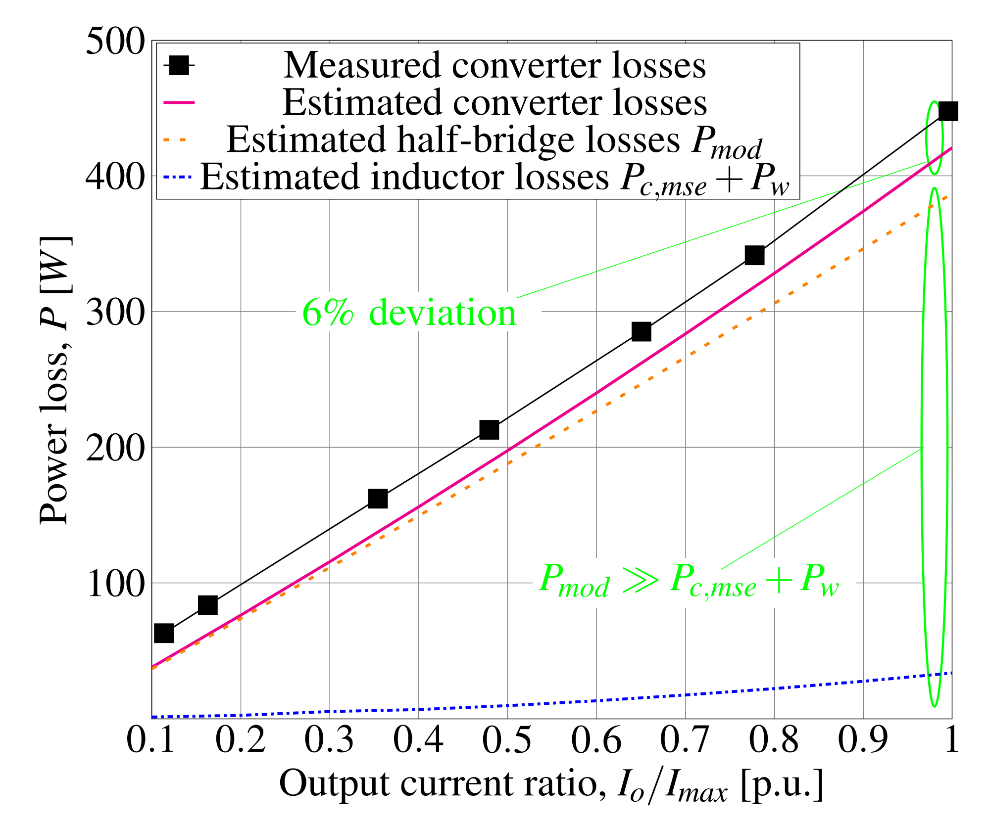
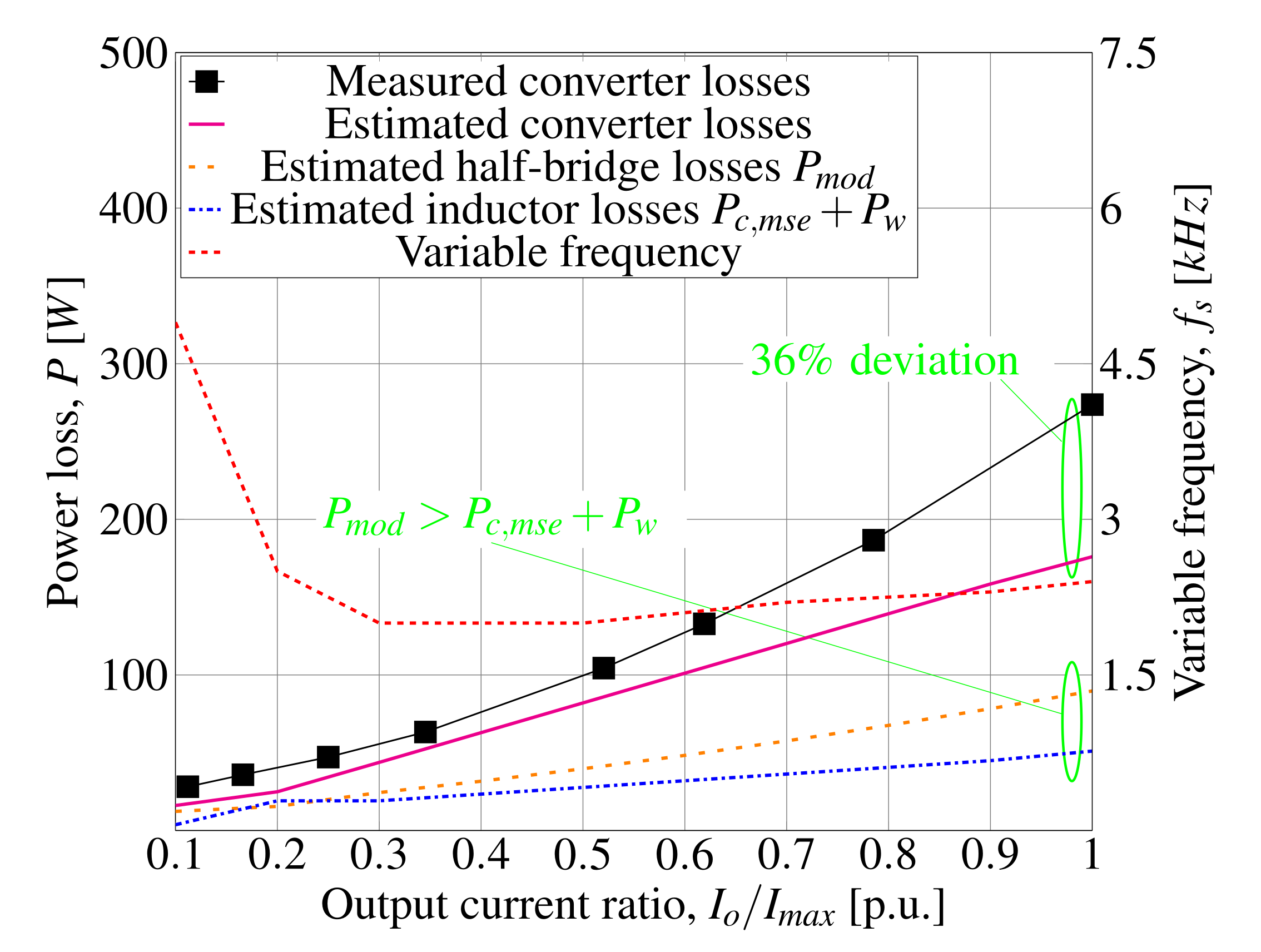
Figure 10 illustrates the power loss distribution for a fixed switching frequency of 20 kHz,
= 0.95 and overlapping input and output voltages of 330 V. According to
Figure 10, it is evident that the power losses of the half-bridge modules dominate overall converter losses. Compared to inductor losses, the half-bridge modules dissipate more losses by a factor of 11. In conclusion, the motivation for the novel modulation method is to decrease the switching frequency to reduce the losses of the half-bridge modules as far as possible to achieve a balanced power loss distribution. Therefore, the aim is to operate in CrCM by adapting (reducing) the switching frequency. Hence, the CrCMASF operates at the boundary limit between CCM and DCM.
It is necessary to ensure an inductance at the maximum current for a specified current ripple for powder core design. The maximum current ripple for this study is approximately 31.2 A with a maximum switching frequency of 20 kHz.
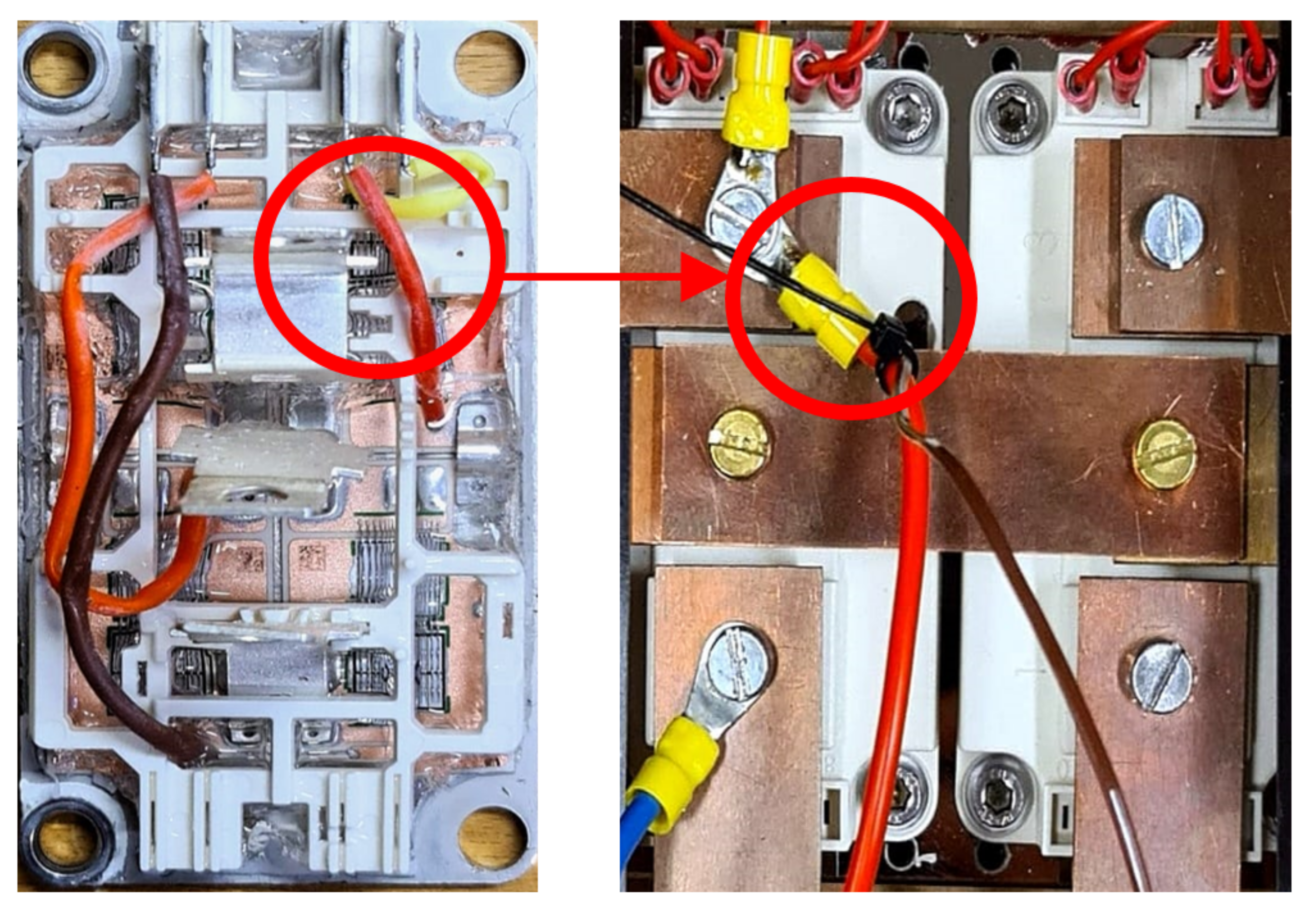
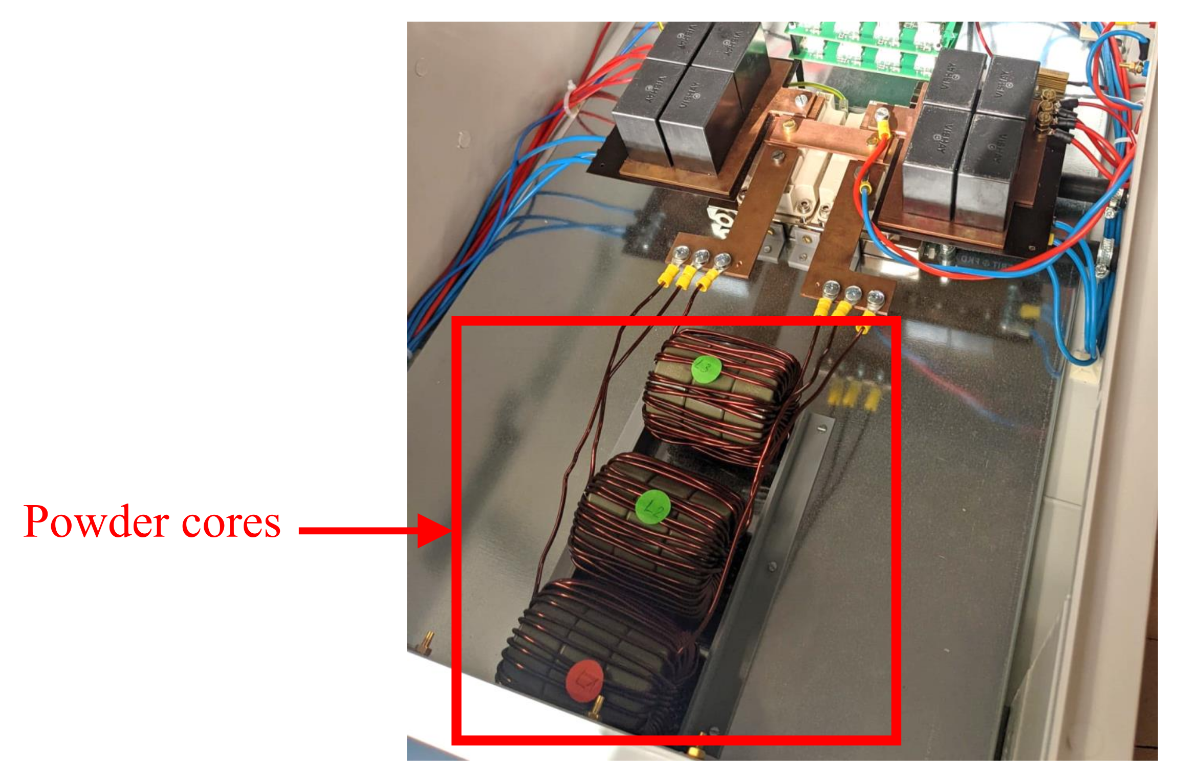
The experimental setup, introduced in the previous section, uses an inductor consisting of three parallel-connected cores (58,617 from magnetics), each with three stacks and 39 turns of winding (size: AWG10) and can be seen in
Figure 11. The inductance at the maximum output current of 60 A is approximately 222
F.
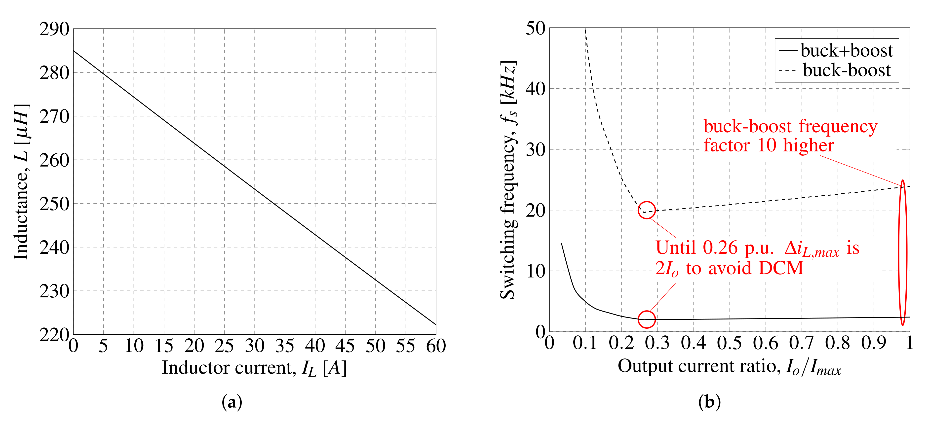
Figure 12a illustrates the behaviour of the inductance
L as a function of the inductor current
.
Figure 12b presents the switching frequency for overlapping input and output voltages of 330 V—Equation (
25) for
≥
or Equation (
26)
≤
:
From
Figure 12b, it is evident that switching frequency modulation is not reasonable for buck–boost mode as the switching frequency
is not below the maximum of 20 kHz at all operation points. However, the switching frequency needs to decrease due to the high power semiconductor switching losses to enhance efficiency. On the other hand, using buck + boost mode, low switching frequencies are possible, enabling efficiency optimisation. The definition of the current ripple
is according to the law of induction and the effective inductor voltage–time areas for both modes in
Figure 4 and
Figure 5. Both figures reveal that these areas are significantly larger for buck–boost mode. In contrast, in buck + boost mode, the inductor is temporarily energised and de-energised simultaneously, enabling low current ripples. The converter also considers a minimum frequency to avoid DCM by using Equations (
25) and (
26), therefore setting the maximum current ripple
according to the boundary limit between DCM and CCM, which is
for output currents of up to 15.6 A (0.26 p.u.). The procedure uses a maximum current ripple of 31.2 A for output currents above 15.6 A. Therefore, for an output current of 60 A, a switching frequency of approximately 2 kHz is possible, as shown in
Figure 12b. With
Figure 12b and Equations (
25) and (
26), it is possible to set the switching frequency for the experimentation phase accordingly.
Figure 13 illustrates the estimated power loss distribution for overlapping input and output voltages of 330 V,
= 0.95, and CrCMASF. Compared to the results in
Figure 10, the introduced CrCMASF significantly reduces power semiconductor losses. However, due to the reduced switching frequency and increased AC flux density, inductor losses increase. Nevertheless, this analysis justifies the CrCMASF, as the losses of half-bridge modules approach inductor losses, reducing overall converter losses. The subsequent section will validate these assumptions further for different fixed duty cycles and input and output voltage ratios.
6. Discussion
The presented results have proven that switching frequency modulation is possible and reasonable for the buck + boost mode in the mid-kW range. However, the simple approach of this study (CrCMASF) for the introduced DC–DC converter is only possible for the mid-kW range, as for converters with lower output powers, the magnetic core losses could represent the majority of converter losses. The authors in [
18,
43,
44] analyse this aspect and show that by decreasing the switching frequency, the switching losses for power semiconductors decrease while core losses increase. Hence, the optimum switching frequency can differ significantly depending on the converter’s electric properties. Therefore, depending on the application, the ratio of losses must be essential for efficiency optimisation when using switching frequency modulation. Another aspect to consider is semiconductor technology. For example, by using SiC-MOSFETs instead of Si-IGBTs, it is possible to decrease the impact of semiconductor losses on converter efficiency. In this case, the cores could mainly impact the converter power losses. Consequently, if cores are the main factor of the total losses, it is reasonable to increase the switching frequency to reduce the AC flux density. However, the results of this study evince that lower switching frequencies are reasonable for the mid-kW range using Si-IGBTs since they are the main factor of converter losses.
The method of switching frequency modulation is already known, as introduced in [
45] for ZVS or in [
31,
43,
45,
46] where the authors predict losses and the reasonable switching frequency with complex algorithms or optimum efficiency tracking as introduced in [
47]. However, the drawback of these approaches is that their applicability is limited to low power ranges. Furthermore, the known methods require an increased effort of computations. In addition, none of these methods uses the soft saturation effect of powder cores.
Regarding the duty cycles for the buck + boost mode, published literature discusses and analyses the optimum not regarding the converter efficiency [
48,
49,
50] or for lower power ranges [
51].
The results of this study prove that a high fixed duty cycle of 0.95 and switching frequency modulation increase efficiency over the entire power range and decrease device junction temperature rise.
In order to compare the introduced approach for the bidirectional cascaded buck and boost converter with the published literature,
Table 2 lists references with their most important properties.
Starting at the top of
Table 2, the authors in [
28] investigate the buck + boost mode for efficiency enhancement in the high-kW range. The authors in [
28] point out that switching frequency reduction for the buck + boost mode is reasonable. The article [
28] demonstrates the calculation of the minimum switching frequency to meet the inductor’s current ripple requirements. Accordingly, the authors reduce the fixed switching frequency (FSF) from 12 kHz to 10 kHz to increase efficiency in the buck + boost mode. However, unlike what is presented in this article, the authors in [
28] do not use an adaptive procedure to operate in CrCM. Instead, they reduce the FSF to 10 kHz for the entire power range in buck + boost mode. Another approach is presented in [
16], where the authors compare FSF with CrCM. The results of [
16] confirm the assumption of this article: in order to operate in the CrCM, the authors have to increase the switching frequency while not exceeding the maximum inductor current ripple. Therefore, it is assumed that the authors in [
16] are not using a magnetic core with the soft-saturation effect. Accordingly, due to the increased switching frequency in CrCM, the converter only achieves efficiencies of up to 95%. Moreover, it is unclear if the results in [
16] also refer to overlapping input and output voltages.
Going down in the power range to compare this article with the literature review presented in the first section, reference [
16] disadvantages disable the authors’ approach for the mid-kW range. Even though using ZVS and ZCS, their switching frequency is ∼33 kHz. The authors in [
16] achieve appropriate efficiencies. However, their methods rely on additional hardware. Another approach is [
14], where the authors realise ZVS using the parasitics of the power semiconductors. Unfortunately, the authors in [
14] do not investigate their method for overlapping input and output voltages. Finally,
Table 2 lists reference [
13]. In [
13], the authors introduce the reduced average inductor current (RAIC) method. Although having a complex approach, the computational effort for realisation is moderate without additional hardware. It would be interesting to investigate the RAIC method for the mid-kW range as the authors in [
13] achieved a converter efficiency of up to 97% for the low-W power range.
By comparing the references in
Table 2 with the introduced approach of this article, namely the CrCMASF, it is evident that the major drawback is its limitation. The usage of CrCMASF is only possible for converters if the power losses of the power semiconductors dominate overall power losses. Moreover, the CrCMASF relies on the soft saturation characteristics of the inductor and is therefore not usable for converters based on, e.g., ferrite cores. Nonetheless, the major advantages of the CrCMASF are its simplicity and significant power loss reduction for efficiency enhancement.


