
Characterization of Irradiated Boron, Carbon-Enriched and Gallium Si-on-Si Wafer Low Gain Avalanche Detectors

 ,
,  and
and
Abstract
:1. Introduction
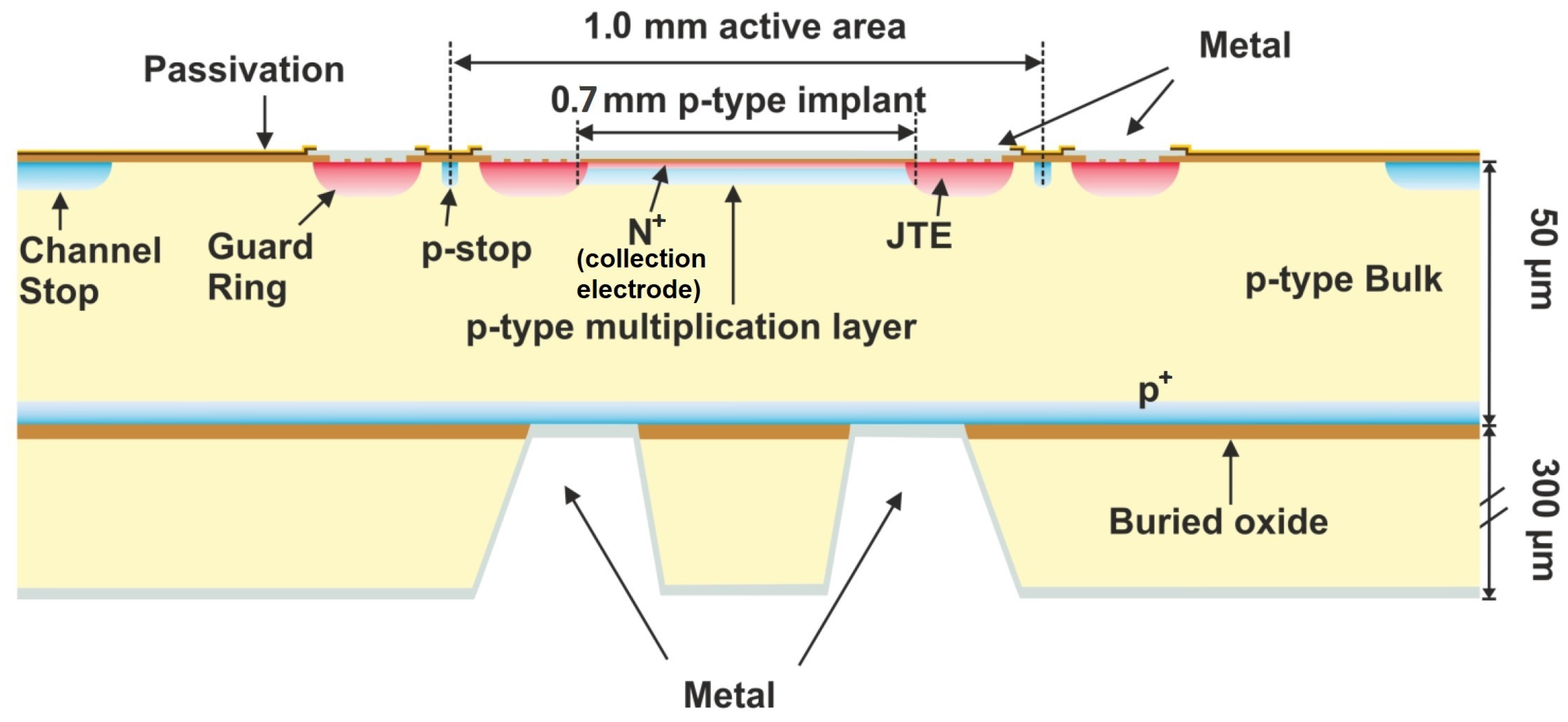
2. Low Gain Avalache Detectors (LGAD)
Samples
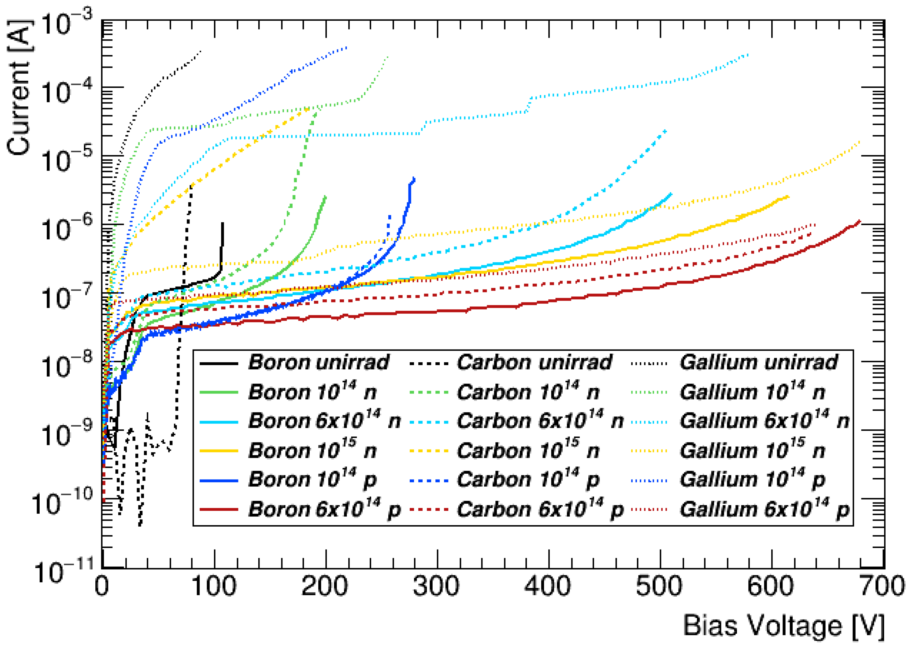
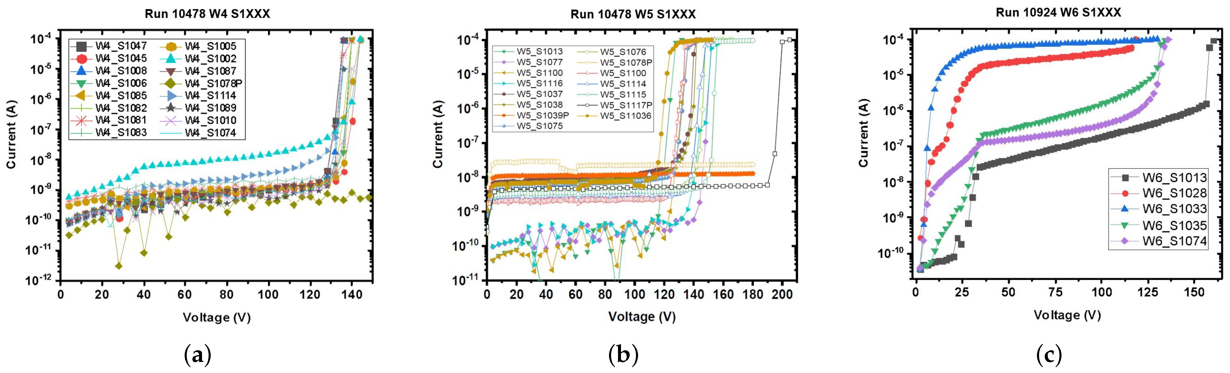
3. Electrical Characterization
4. Transient Current Technique Measurements
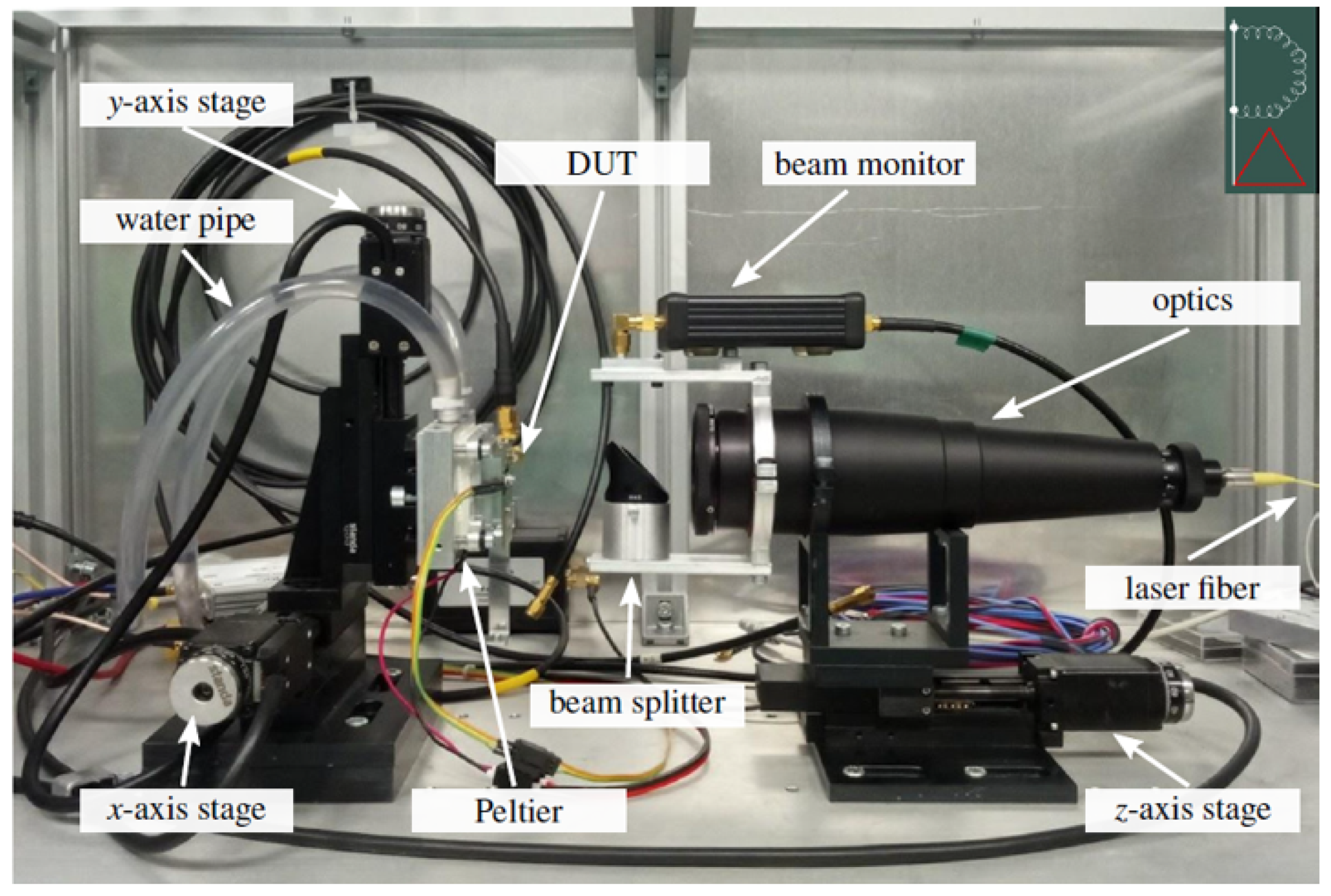
4.1. Experimental Setup
- Two laser sources, Red ( 660 ) and Infra-Red ( 1064 );
- An optical system to focus the laser beam;
- A current amplifier (Particulars wide band current amplifier 35 dB);
- A waveform digitizer (A DRS oscilloscope [23]);
- A set of movable stages that allows to move the sensor on the perpendicular plane with respect to the laser beam and along the beam axis;
- A Peltier element and controller to regulate the operational temperature of the device under test (DUT);
- A beam monitor to check the intensity of the laser beam during the measurement;
- A beam splitter serving as an attenuator and transmittin 30% of the incident light to the DUT plane;
- A dry air filter to avoid condensation for measurements at low temperature.
4.2. Procedure
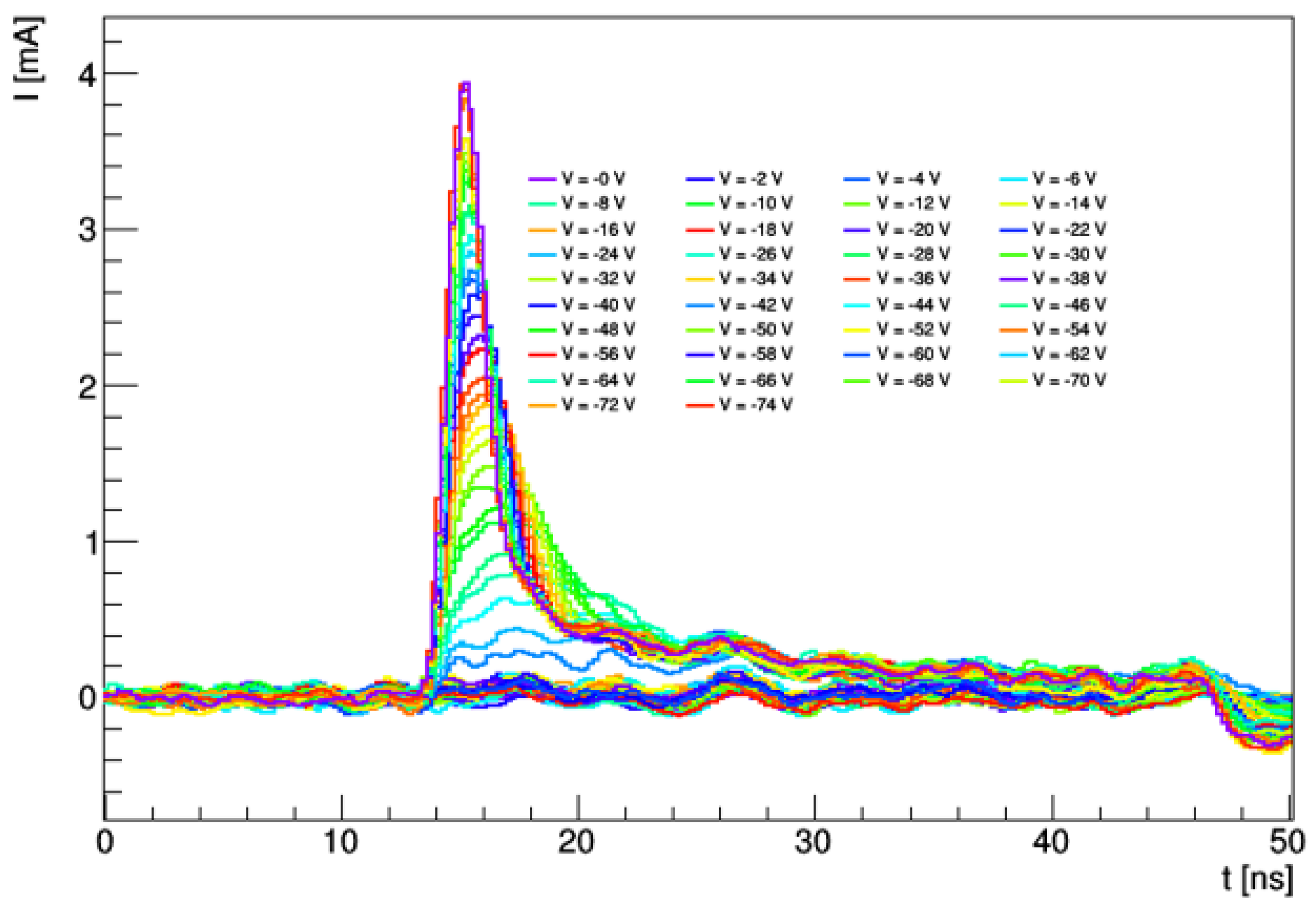
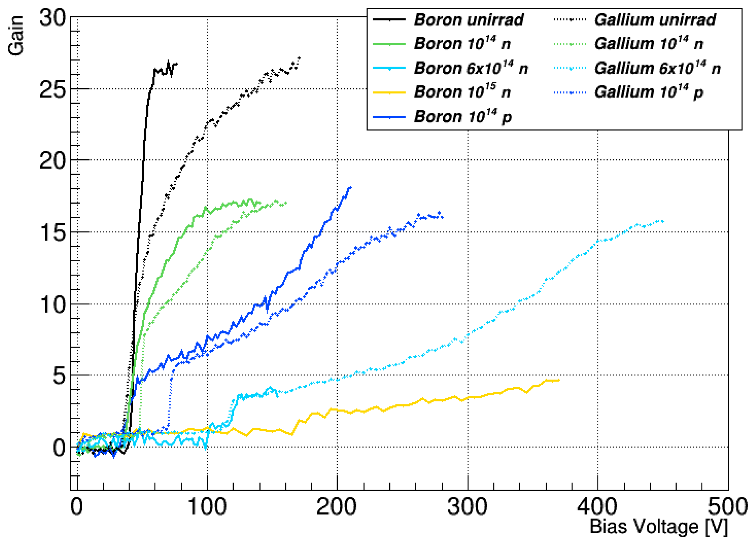
4.3. Gain
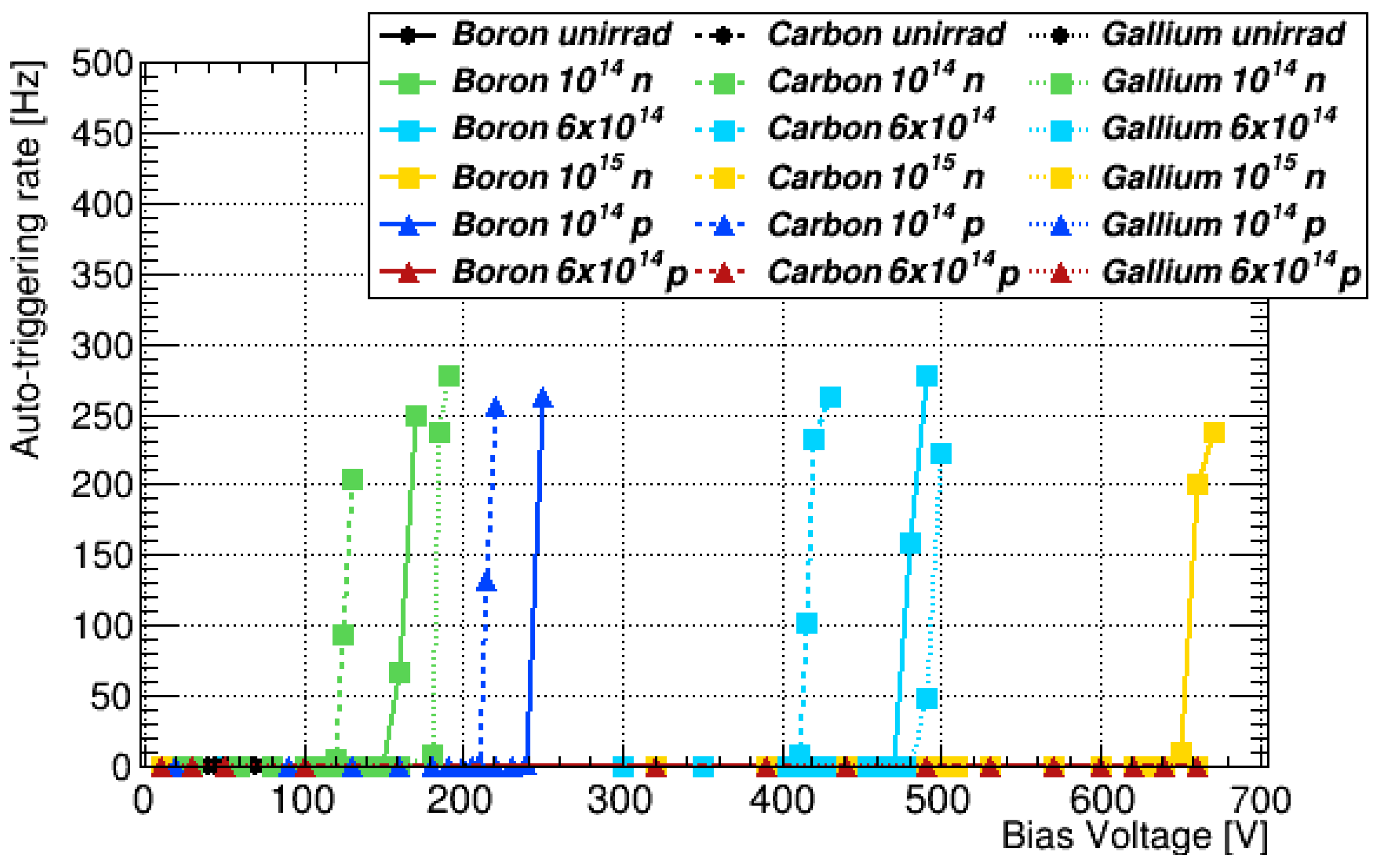
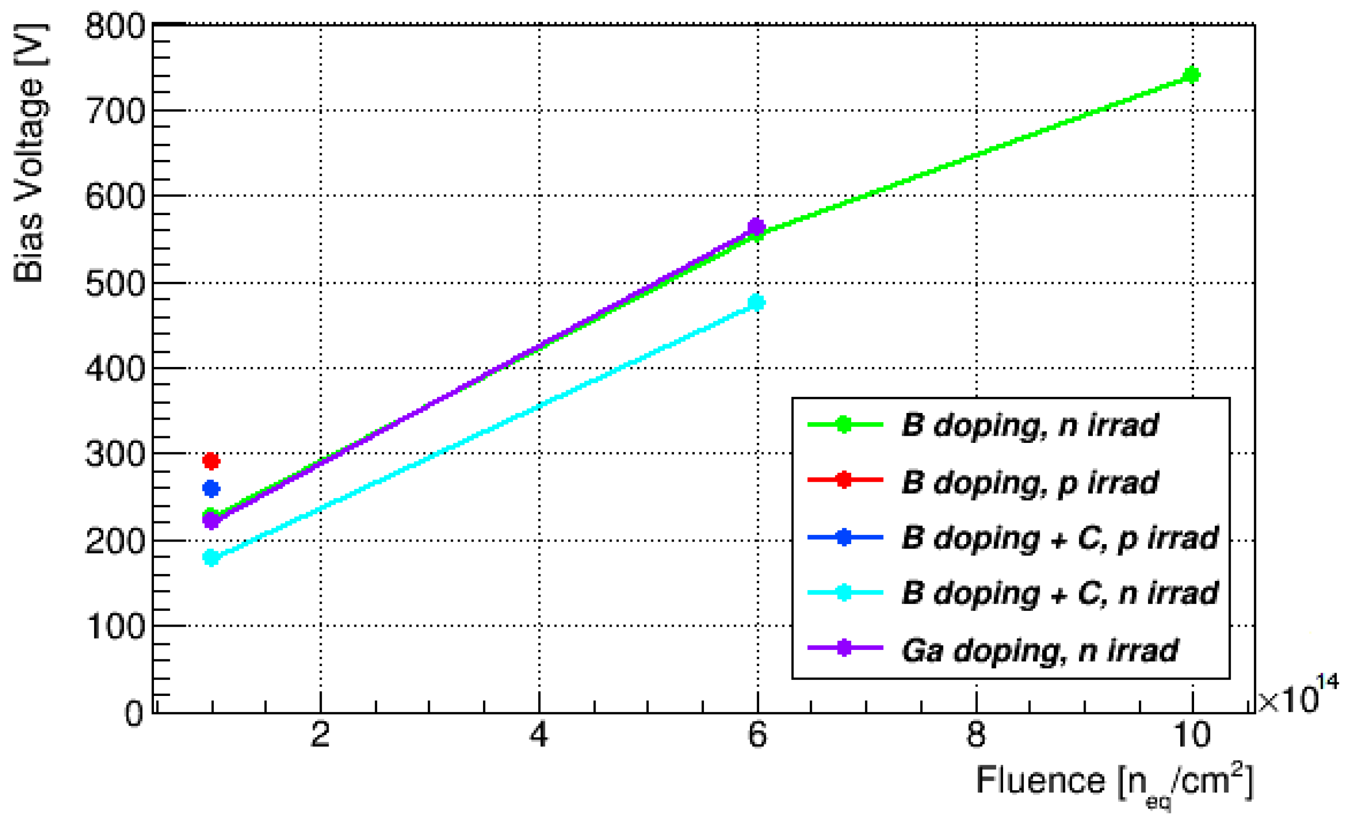
5. Stability Studies
6. Charged-Particle Measurements
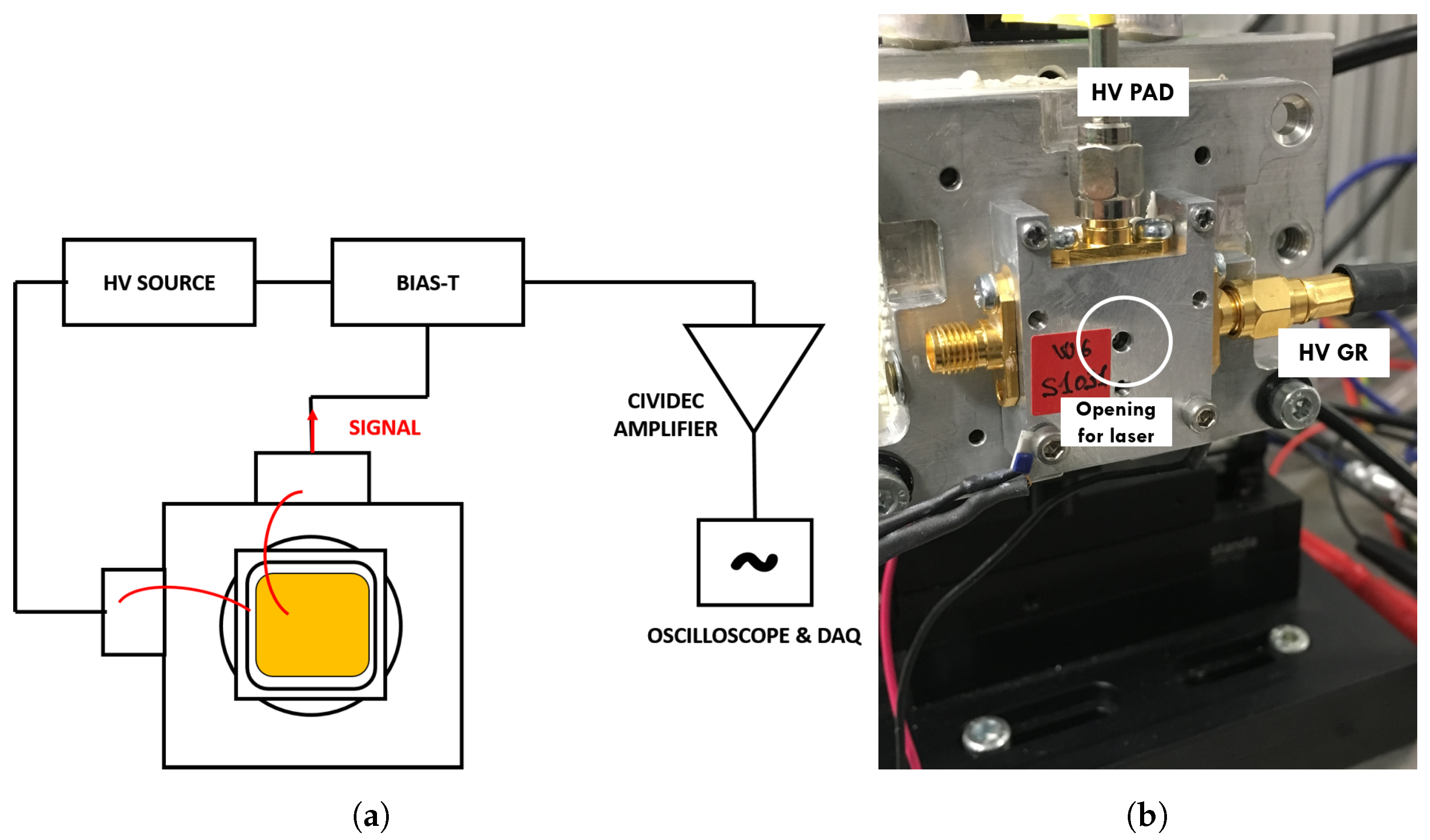
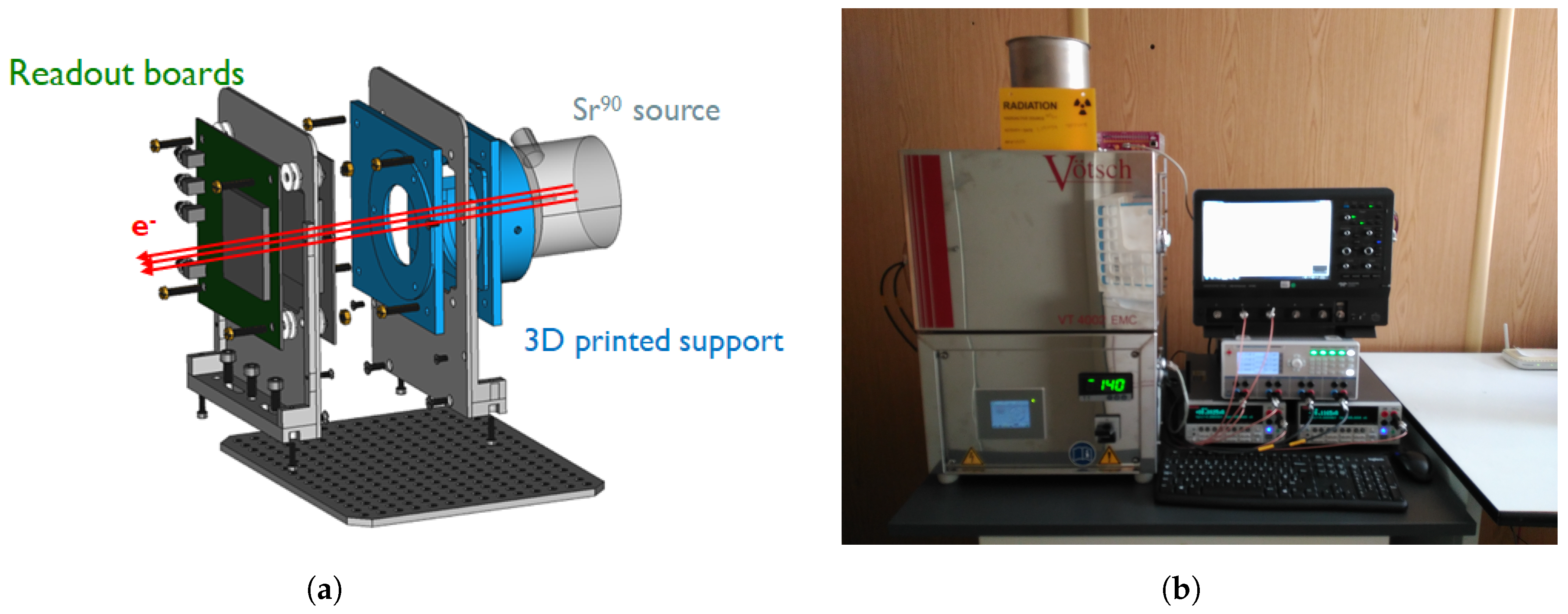
6.1. Experimental Setup
6.2. Procedure
6.3. DAQ and Control System
6.4. Analysis Software
6.5. Collected Charge
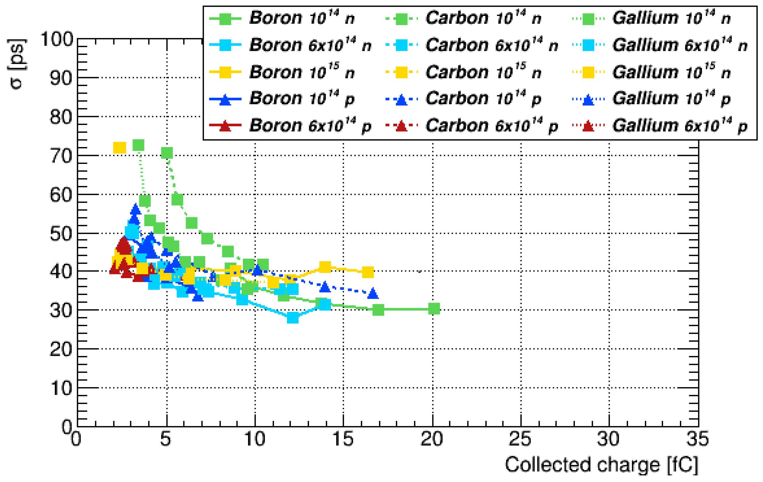
6.6. Time Resolution
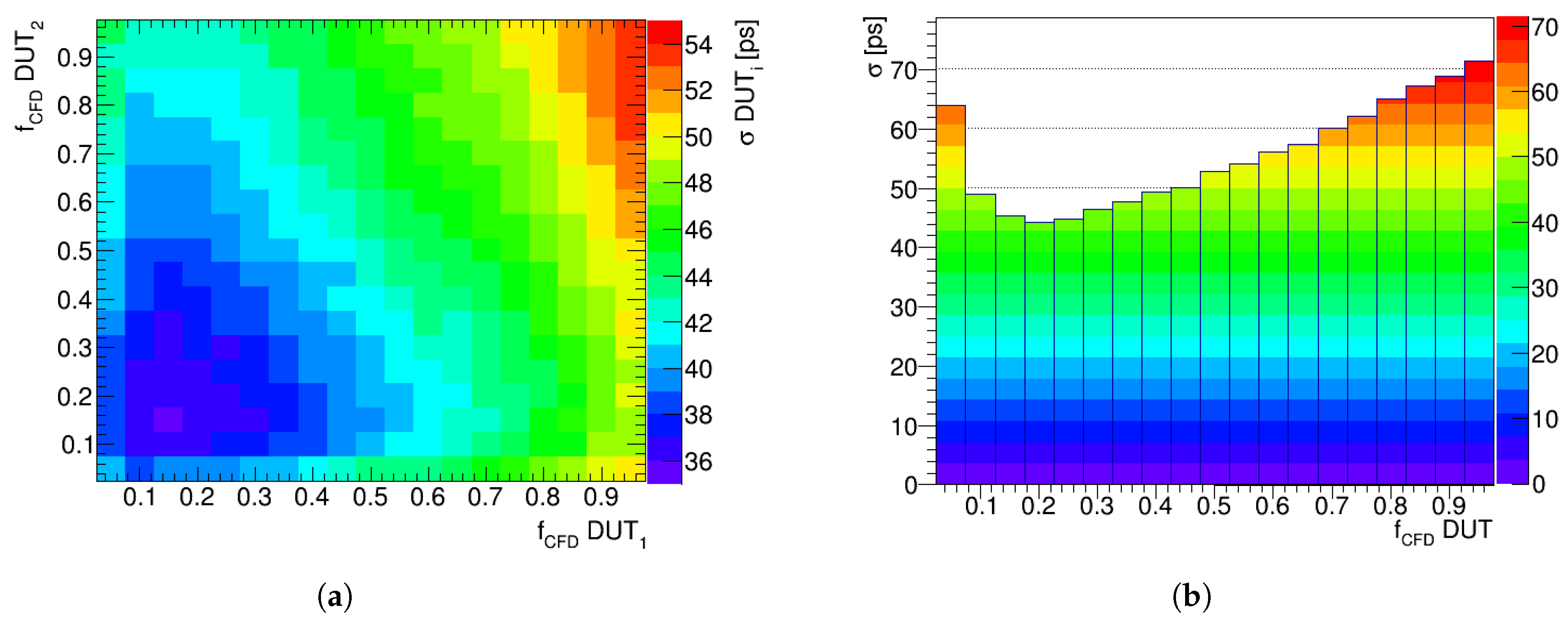
6.6.1. CFD Optimization
7. Conclusions and Outlook
Author Contributions
Funding
Institutional Review Board Statement
Informed Consent Statement
Data Availability Statement
Acknowledgments
Conflicts of Interest
Abbreviations
| IFAE | Institut de Física d’Altes Energies |
| BIST | Barcelona Institute of Science and Technology |
| CERN | Conseil Européen pour la Recherche Nucléaire |
| CNM | Centro Nacional de Microelectrónica |
| LGAD | Low Gain Avalanche Detector |
| MIP | Minimum Ionizing Particle |
| HL-LHC | High-Luminosity Large Hadron Collider |
| HGTD | High-Granularity Timing Detector |
| ETL | End-cap Timing Layer |
| I-V | Current-Voltage |
| C-V | Capacitance-Voltage |
| TCT | Transient Current Technique |
| LHC | Large Hadron Collider |
| ITk | Inner Tracker |
| PV | Primary Vertex |
| JTE | Junction Termination Extension |
| SSD | Solid State Detectors |
| IR | Infra-Red |
| DUT | Device Under Test |
| DAQ | Data Acquisition |
| TOA | Time Of Arrival |
| CFD | Constant Fraction Discriminator |
| TOT | Time-Over-Threshold |
Appendix A. Additional Results
Appendix A.1. I-V Curves at Room Temperature

Appendix A.2. Time Resolution Behavior with Charge

Appendix A.3. CFD Fraction Behavior with Fluence

Appendix A.4. Other Signal Properties
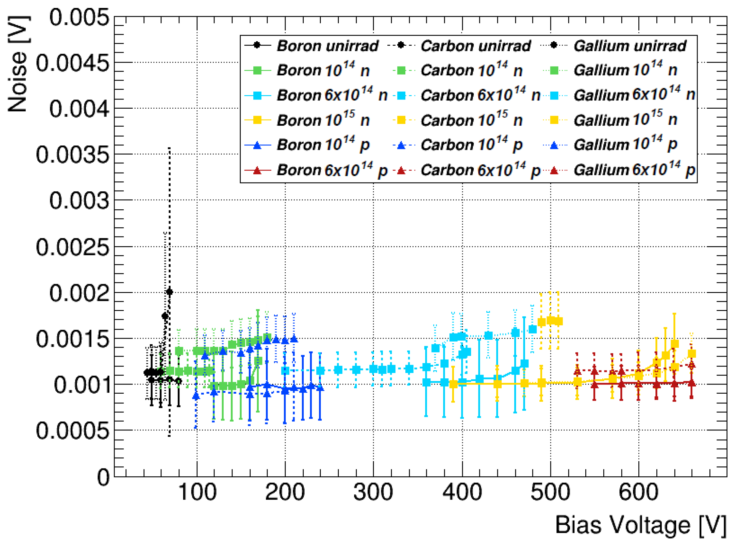
Appendix A.4.1. Noise

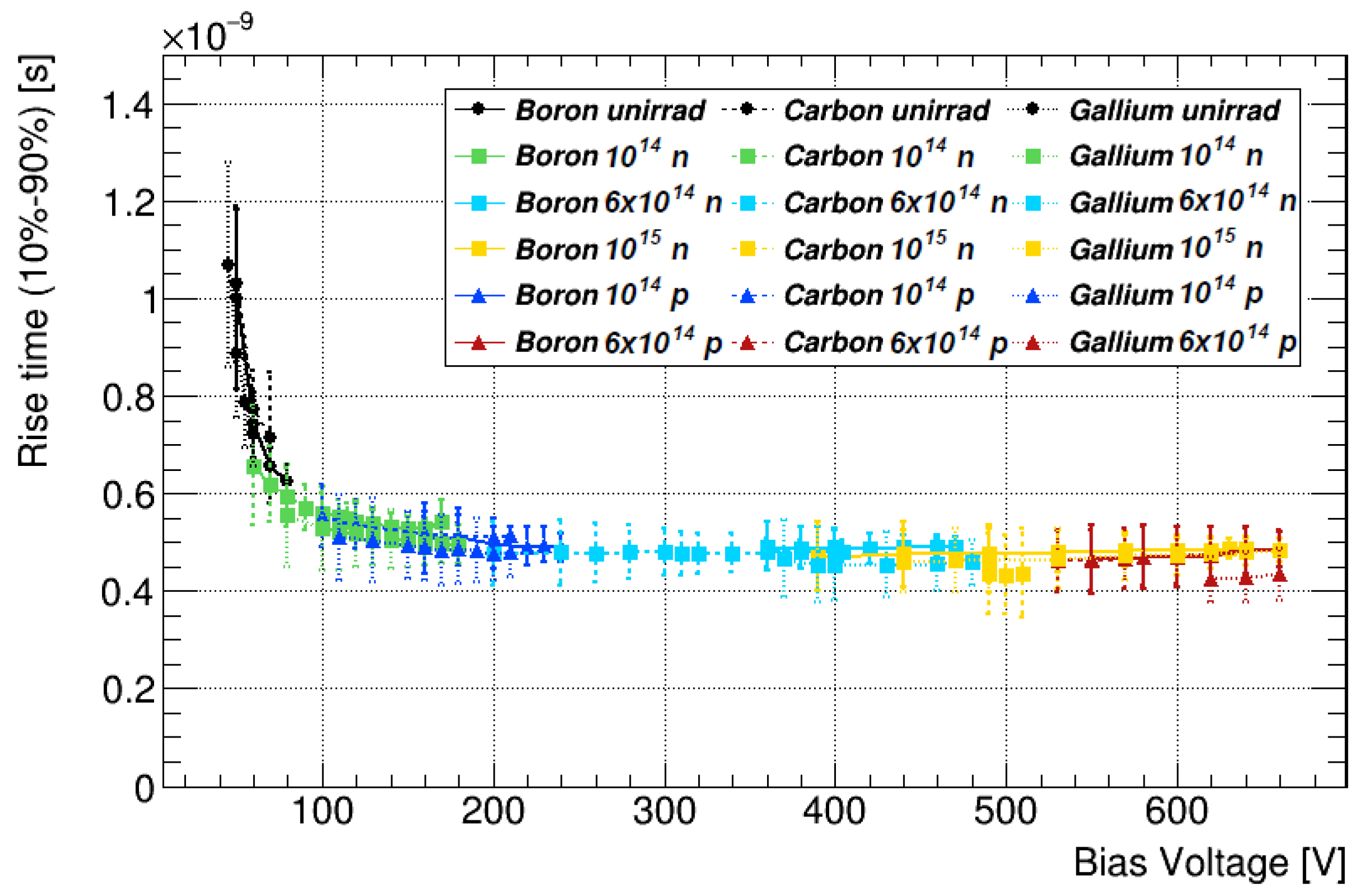
Appendix A.4.2. Rise Time

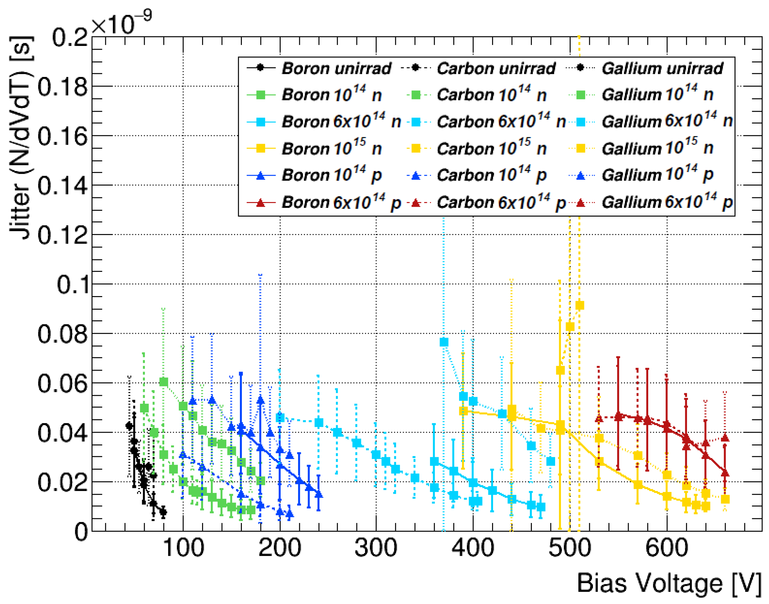
Appendix A.4.3. Jitter

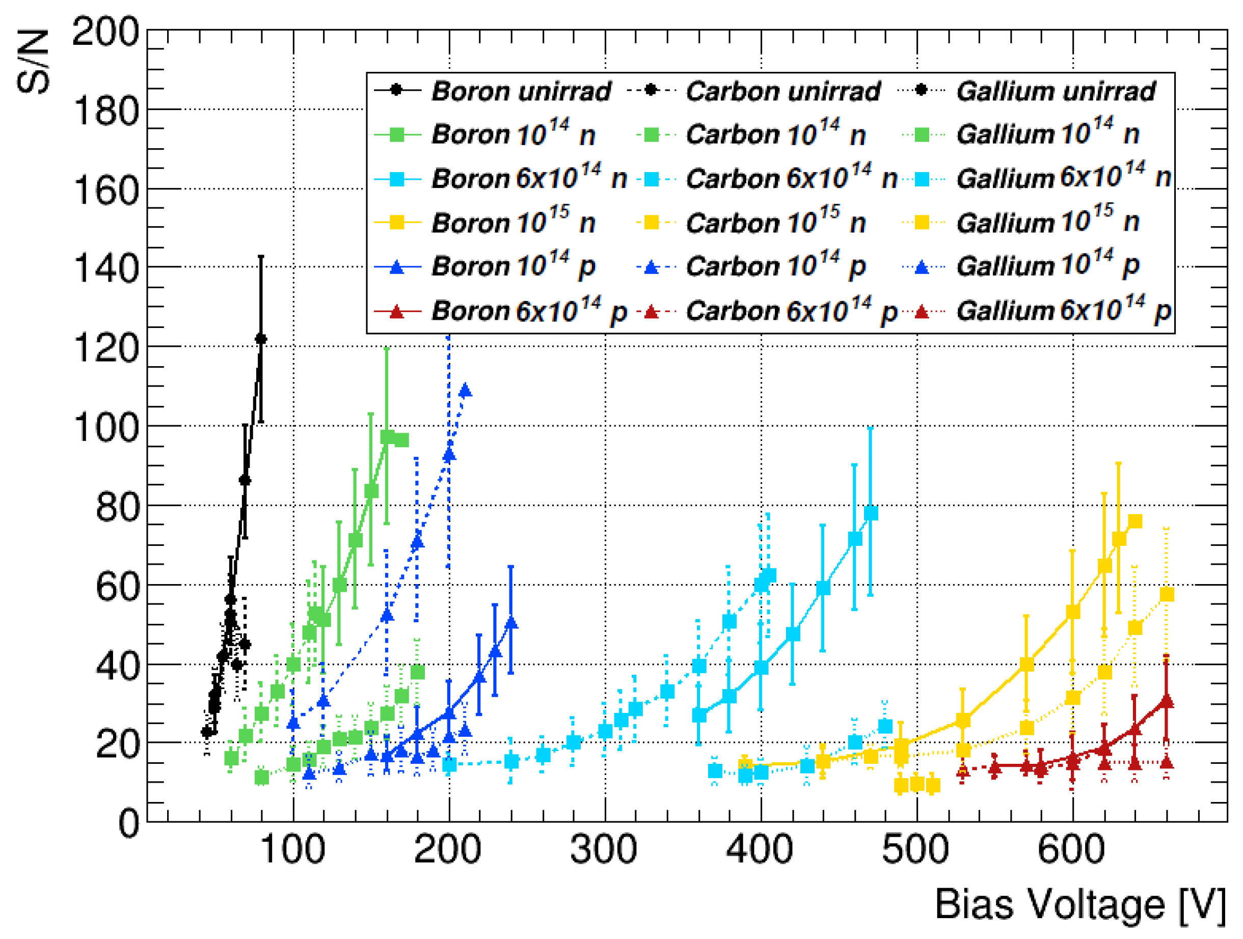
Appendix A.4.4. Signal-to-Noise Ratio

References
- Rossi, L.; Brüning, O. High Luminosity Large Hadron Collider: A Description for the European Strategy Preparatory Group; Technical Report CERN-ATS-2012-236; CERN: Geneva, Switzerland, 2012. [Google Scholar]
- Apollinari, G.; Béjar Alonso, I.; Brüning, O.; Fessia, P.; Lamont, M.; Rossi, L.; Tavian, L. High-Luminosity Large Hadron Collider (HL-LHC): Technical Design Report V. 0.1; CERN Yellow Reports: Monographs; CERN: Geneva, Switzerland, 2017. [Google Scholar] [CrossRef]
- The ATLAS Collaboration. The ATLAS Experiment at the CERN Large Hadron Collider. J. Instrum. 2008, 3, S08003. [Google Scholar] [CrossRef] [Green Version]
- The CMS Collaboration. The CMS experiment at the CERN LHC. J. Instrum. 2008, 3, S08004. [Google Scholar] [CrossRef] [Green Version]
- The ATLAS Collaboration. Technical Design Report for the ATLAS Inner Tracker Pixel Detector; Technical Report CERN-LHCC-2017-021, ATLAS-TDR-030; CERN: Geneva, Switzerland, 2017. [Google Scholar]
- Sadrozinski, H.F.W.; Seiden, A.; Cartiglia, N. 4-Dimensional Tracking with Ultra-Fast Silicon Detectors. arXiv 2017, arXiv:1704.08666. [Google Scholar]
- Pellegrini, G.; Fernández-Martínez, P.; Baselga, M.; Fleta, C.; Flores, D.; Greco, V.; Hidalgo, S.; Mandić, I.; Kramberger, G.; Quirion, D.; et al. Technology developments and first measurements of Low Gain Avalanche Detectors (LGAD) for high energy physics applications. Nucl. Instrum. Methods Phys. Res. Sect. A Accel. Spectrometers Detect. Assoc. Equip. 2014, 765, 12–16. [Google Scholar] [CrossRef]
- The ATLAS Collaboration. Technical Proposal: A High-Granularity Timing Detector for the ATLAS Phase-II Upgrade; Technical Report CERN-LHCC-2018-023. LHCC-P-012; CERN: Geneva, Switzerland, 2018. [Google Scholar]
- The CMS Collaboration. Technical Proposal for A MIP Timing Detector in the CMS Experiment Phase 2 Upgrade; Technical Report CERN-LHCC-2017-027. LHCC-P-009; CERN: Geneva, Switzerland, 2017. [Google Scholar]
- Williams, M. The LHCb VELO Upgrade II. In Proceedings of the International Workshop on Semiconductor Pixel Detectors for Particles and Imaging (PIXEL2018), Taipei, Taiwan, 10–14 December 2018; Available online: https://indico.cern.ch/event/669866/contributions/3235374/ (accessed on 25 December 2021).
- Pellegrini, G.; Carulla, M.; Flores, D.; Hidalgo, S.; Quirion, D. Status of LGAD productions at CNM. In Proceedings of the 30th RD50 Workshop, Krakow, Poland, 5–7 June 2017; Available online: https://indico.cern.ch/event/637212/contributions/2608652/ (accessed on 25 December 2021).
- Hidalgo, S.; Carulla, M.; Doblas, A.; Flores, D.; Merlos, A.; Pellegrini, G.; Quirion, D. CNM activities on LGADs for ATLAS/CMS Timing Layers. In Proceedings of the 32th RD50 Workshop, Hamburg, Germany, 4–6 June 2018; Available online: https://indico.cern.ch/event/719814/contributions/3022492/ (accessed on 25 December 2021).
- Carulla, M. Thin LGAD Timing Detectors for the ATLAS Experiment; Universitat Autonoma de Barcelona: Barcelona, Spain, 2019; Available online: https://www.tesisenred.net/handle/10803/667283#page=1 (accessed on 25 December 2021).
- Lange, J.; Carulla, M.; Cavallaro, E.; Chytka, L.; Davis, P.; Flores, D.; Förster, F.; Grinstein, S.; Hidalgo, S.; Komarek, T.; et al. Gain and time resolution of 45 μm thin Low Gain Avalanche Detectors before and after irradiation up to a fluence of 1015 neq/cm2. J. Instrum. 2017, 12, P05003. [Google Scholar] [CrossRef] [Green Version]
- Cavallaro, E. Novel Silicon Detector Technologies for the HL-LHC ATLAS Upgrade; Universitat Autonoma de Barcelona: Barcelona, Spain, 2018; Available online: https://www.tesisenred.net/handle/10803/666621#page=1 (accessed on 25 December 2021).
- Allaire, C.; Benitez, J.; Bomben, M.; Calderini, G.; Carulla, M.; Cavallaro, E.; Falou, A.; Flores, D.; Freeman, P.; Galloway, Z.; et al. Beam test measurements of Low Gain Avalanche Detector single pads and arrays for the ATLAS High Granularity Timing Detector. J. Instrum. 2018, 13, P06017. [Google Scholar] [CrossRef]
- The RD50 Collaboration. Available online: https://rd50.web.cern.ch/rd50 (accessed on 25 December 2021).
- 2410 Sourcemeter Datasheet. Available online: https://www.tek.com/en/sitewide-content/datasheets/s/e/r/series-2400-sourcemeter-instruments (accessed on 25 December 2021).
- Gkougkousis, E.L.; Garcia, L.C.; Grinstein, S.; Coco, V. Comprehensive technology study of radiation hard LGADs. arXiv 2021, arXiv:2111.06731. [Google Scholar]
- Gkougkousis, E.L.; Castillo García, L.; Coco, V. A comparative study of LGAD radiation damage mechanisms. In Proceedings of the Workshop on Pico-Second Timing Detectors for Physics, Zurich, Switzerland, 9–11 September 2021; Available online: https://indico.cern.ch/event/861104/contributions/4514659/ (accessed on 25 December 2021).
- Kramberger, G. Advanced Transient Current Technique Systems. In Proceedings of the 23rd International Workshop on Vertex Detectors (Vertex 2014), Doksy, Czech Republic, 15–19 September 2014. [Google Scholar]
- Simon Argemi, L.; Grinstein, S.; Lange, J. TCT Measurements on 3D Small Pitch Strip Detectors, 2016. Master’s Thesis, Universitat Autonoma de Barcelona, Barcelona, Spain, 2016. [Google Scholar]
- Ritt F, S.; Dinapoli, R.; Hartmann, J. Application of the DRS Chip for Fast Waveform Digitizing. Nucl. Instrum. Methods Phys. Res. A 2010, 623, 486–488. [Google Scholar] [CrossRef]
- Lecroy 8000 Datasheet. Available online: http://cdn.teledynelecroy.com/files/pdf/waverunner8000-datasheet.pdf (accessed on 25 December 2021).
- Galloway, Z.; Fadeyev, V.; Freeman, P.; Gkougkousis, E.; Gruey, B.; Labitan, C.A.; Luce, Z.; McKinney-Martinez, F.; Sadrozinski, H.F.W.; Seiden, A.; et al. Properties of HPK UFSD after neutron irradiation up to 6e15 n/cm2. arXiv 2017, arXiv:1707.04961. [Google Scholar] [CrossRef] [Green Version]
- Rohde & Schwarz Hmp Power Supplies User MANUAL. Available online: https://scdn.rohde-schwarz.com/ur/pws/dl_downloads/dl_common_library/dl_manuals/gb_1/h/hmp_serie/HMPSeries_UserManual_en_02.pdf (accessed on 25 December 2021).
- LGADUtils: A C++ Based Framework for Waveform Analysis. Available online: https://gitlab.cern.ch/egkougko/lgadutils (accessed on 25 December 2021).
- Castillo García, L. A High-Granularity Timing Detector for the Phase-II upgrade of the ATLAS Calorimeter system: Detector concept, description and R&D and beam test results. J. Instrum. 2020, 15, C09047. [Google Scholar]
- Kramberger, G. LGADs for Timing Detectors at HL-LHC; Jožef Stefan Institute: Ljubljana, Slovenia, 2021; Available online: https://indico.cern.ch/event/1088953/ (accessed on 25 December 2021).
- Grieco, C. Overview of CNM LGAD results: Boron Si-on-Si and epitaxial wafers. In Proceedings of the 12th International Conference on Position Sensitive Detectors, Birmingham, UK, 12–17 September 2021. [Google Scholar]
- Sadrozinski, H. Timing Resolution Measurements on Utra-fast Silicon Detectors. In Proceedings of the International `Hiroshima’ Symposium on the Development and Application of Semiconductor Tracking Detectors (HSTD-11), Okinawa, Japan, 10–15 December 2017; Available online: https://indico.cern.ch/event/577879/contributions/2740418/ (accessed on 25 December 2021).
- Lastovicka-Medin, G.; Andreasson, J.; Cartiglia, N.; Černý, J.; Kramberger, G.; Kroll, J.; Kropielniczki, K.; Lastovicka, T.; Rebarz, M.; Sola, V.; et al. First LGAD timing/jitter measurement at ELI with fs-lasers of 800 nm and 1450 nm. In Proceedings of the 36th RD50 Workshop, Zurich, Switzerland, 3–5 June 2020; Available online: https://indico.cern.ch/event/918298/contributions/3880602/ (accessed on 25 December 2021).


| Run | Wafer | Implant | Un-Irrad | n/cm | n/cm | n/cm | Irradiation Type |
|---|---|---|---|---|---|---|---|
| 10478 | W4 | Boron | S1022 | S1095 | S1016 | S1068 | neutron |
| S1067 | S1064 | proton | |||||
| W5 | Boron+ | S1013 | S1005 | S1008 | S1009 | neutron | |
| C-enriched | S1038 | S1076 | proton | ||||
| 10924 | W6 | Gallium | S1021 | S1007 | S1012 | S1009 | neutron |
| S1023 | S1036 | proton |
| Production Run | Wafer | Sensor | Implant | Fluence [n/cm] | Irradiation Type | Size |
|---|---|---|---|---|---|---|
| 10478 | W4 | S1022 | Boron | Unirradiated | - | 1 × 1 mm |
| 10478 | W4 | S1067 | Boron | proton | 1 × 1 mm | |
| 10478 | W4 | S1095 | Boron | neutron | 1 × 1 mm | |
| 10478 | W4 | S1016 | Boron | neutron | 1 × 1 mm | |
| 10478 | W4 | S1068 | Boron | neutron | 1 × 1 mm | |
| 10924 | W6 | S1039P | - | Unirradiated PIN diode | - | 1 × 1 mm |
| 10924 | W6 | S1041 | Gallium | Unirradiated | - | 1 × 1 mm |
| 10924 | W6 | S1044 | Gallium | proton | 1 × 1 mm | |
| 10924 | W6 | S1007 | Gallium | neutron | 1 × 1 mm | |
| 10924 | W6 | S1012 | Gallium | neutron | 1 × 1 mm |
Publisher’s Note: MDPI stays neutral with regard to jurisdictional claims in published maps and institutional affiliations. |
© 2021 by the authors. Licensee MDPI, Basel, Switzerland. This article is an open access article distributed under the terms and conditions of the Creative Commons Attribution (CC BY) license (https://creativecommons.org/licenses/by/4.0/).
Share and Cite
Castillo García, L.; Gkougkousis, E.L.; Grieco, C.; Grinstein, S. Characterization of Irradiated Boron, Carbon-Enriched and Gallium Si-on-Si Wafer Low Gain Avalanche Detectors. Instruments 2022, 6, 2. https://doi.org/10.3390/instruments6010002
Castillo García L, Gkougkousis EL, Grieco C, Grinstein S. Characterization of Irradiated Boron, Carbon-Enriched and Gallium Si-on-Si Wafer Low Gain Avalanche Detectors. Instruments. 2022; 6(1):2. https://doi.org/10.3390/instruments6010002
Chicago/Turabian StyleCastillo García, Lucía, Evangelos Leonidas Gkougkousis, Chiara Grieco, and Sebastian Grinstein. 2022. "Characterization of Irradiated Boron, Carbon-Enriched and Gallium Si-on-Si Wafer Low Gain Avalanche Detectors" Instruments 6, no. 1: 2. https://doi.org/10.3390/instruments6010002