Smart Arbitrary Waveform Generator with Digital Feedback Control for High-Voltage Electrochemistry


Abstract
:1. Introduction
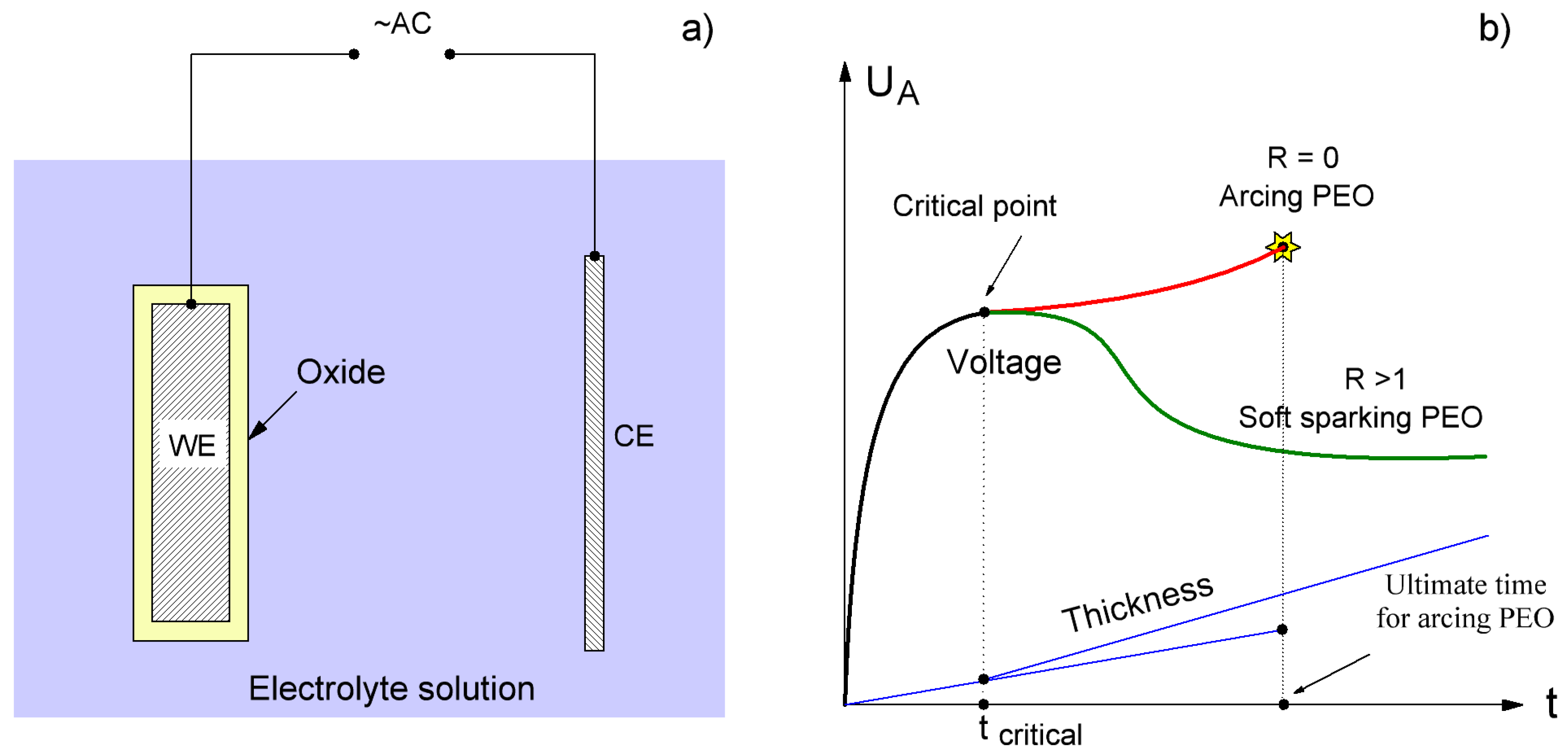
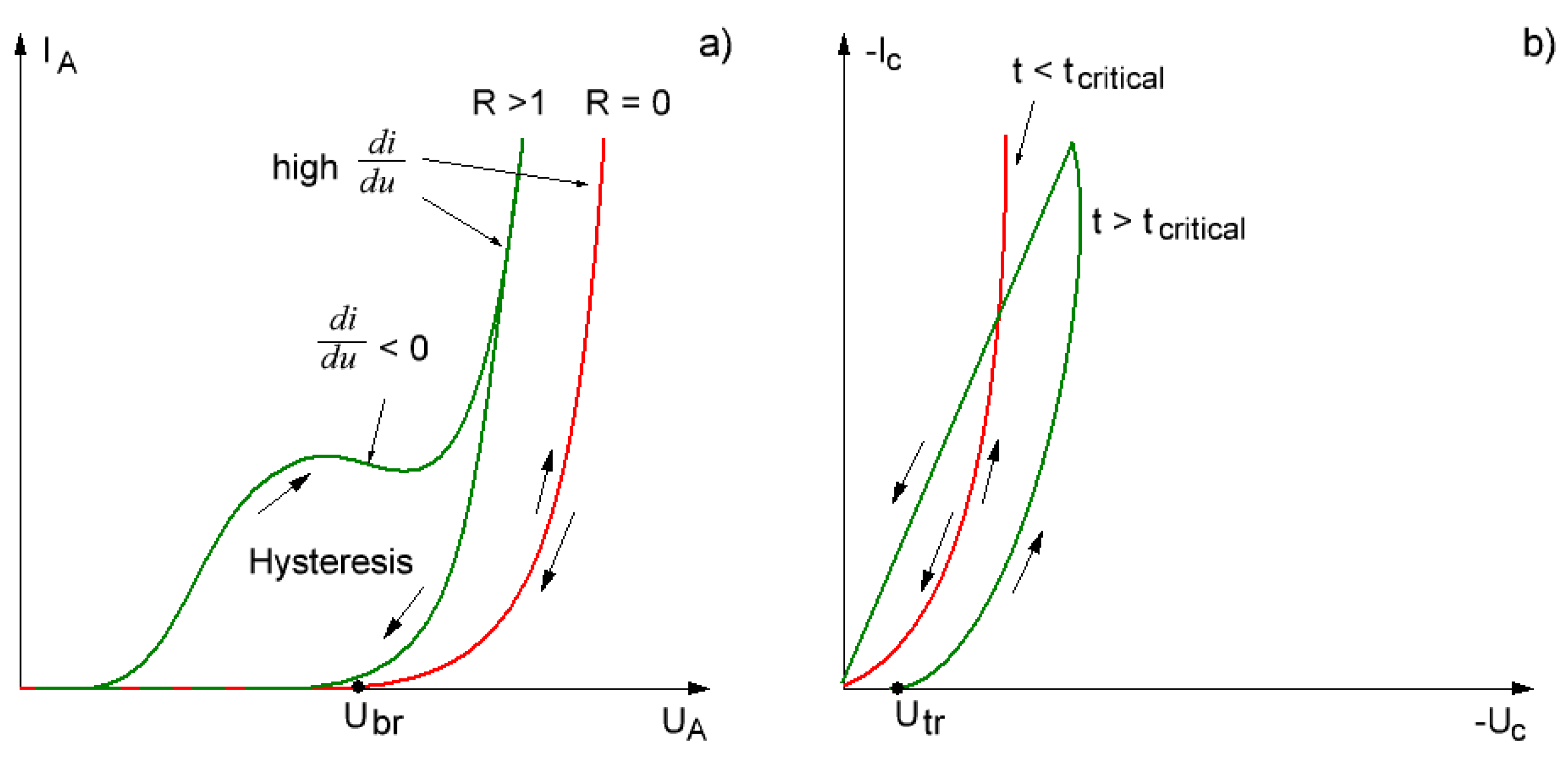
2. Load Analysis
3. System Design
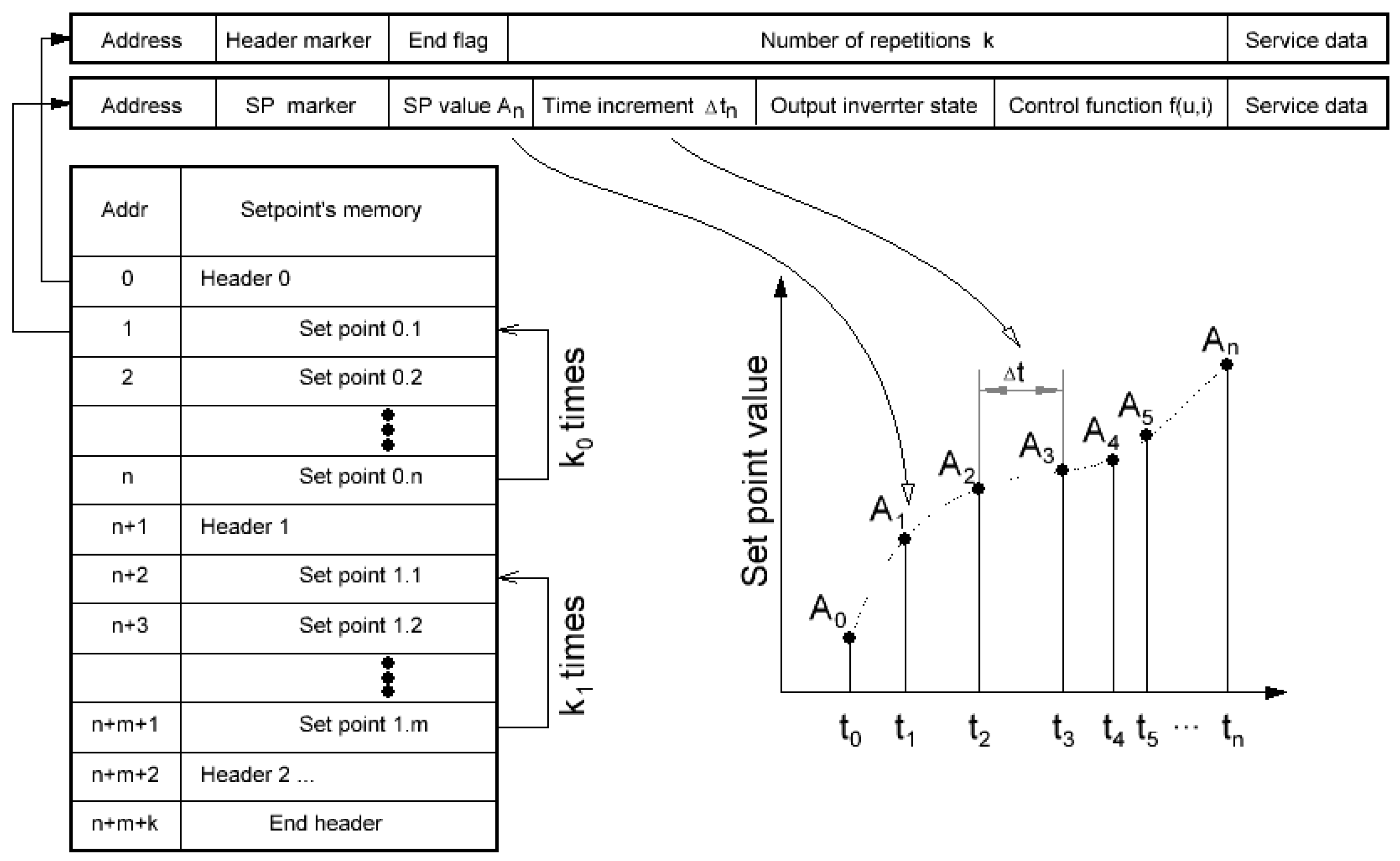
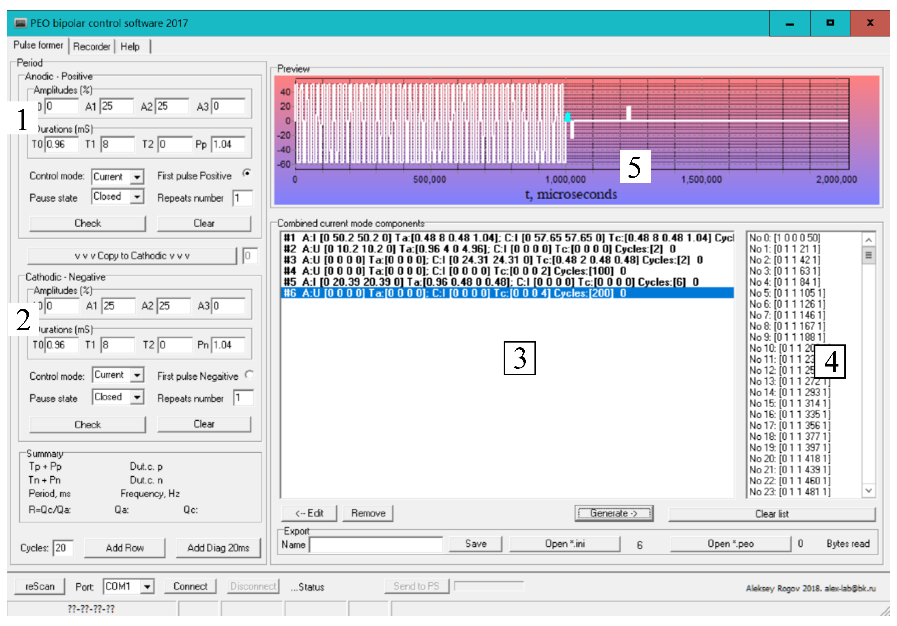
3.1. Waveform Shape Generation
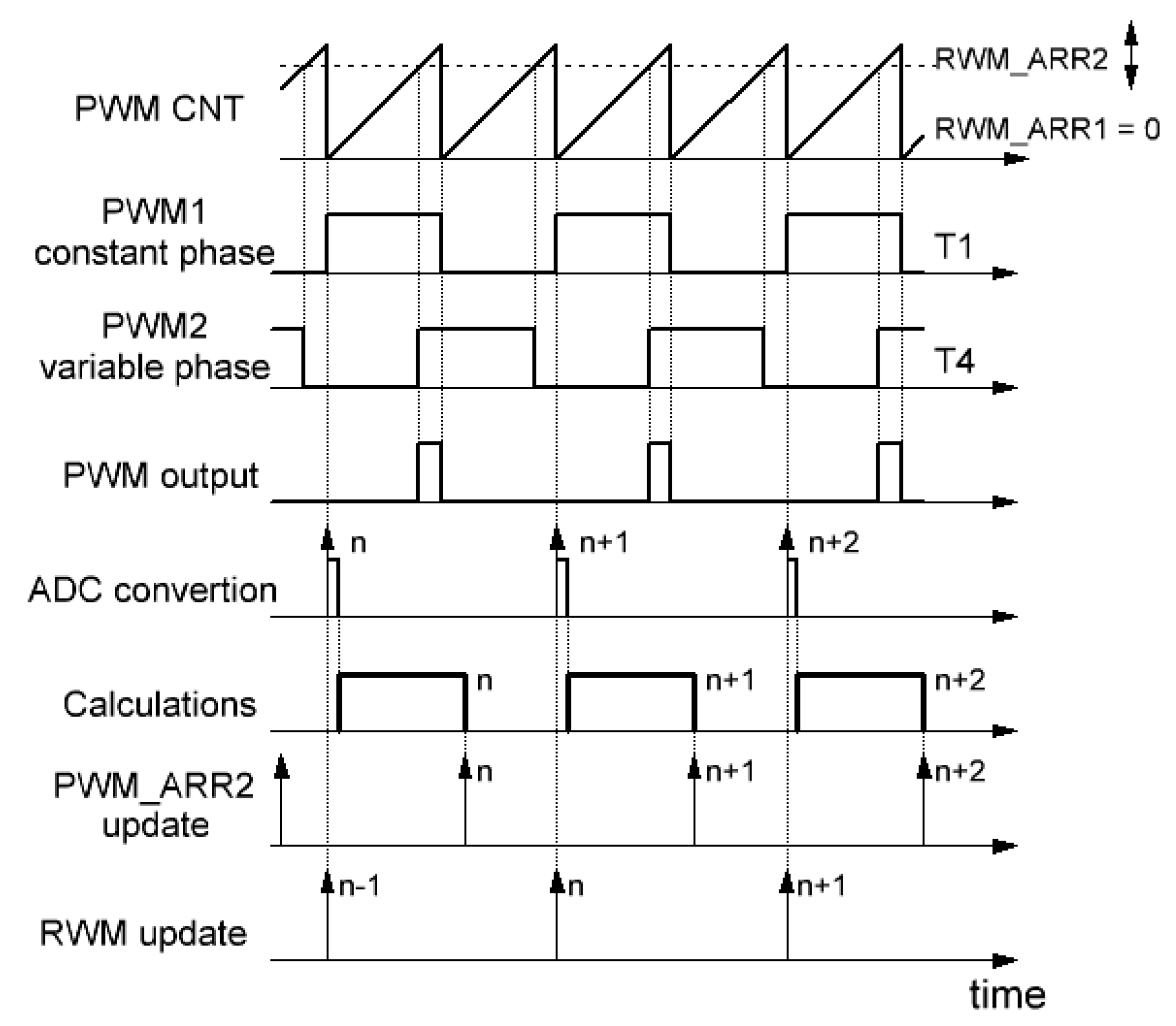
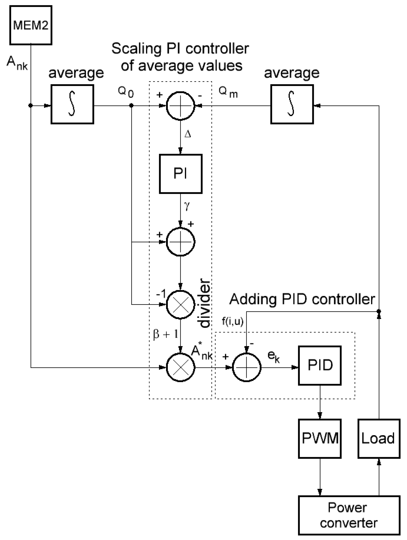
3.2. Correction of the Long-Term Inaccuracies
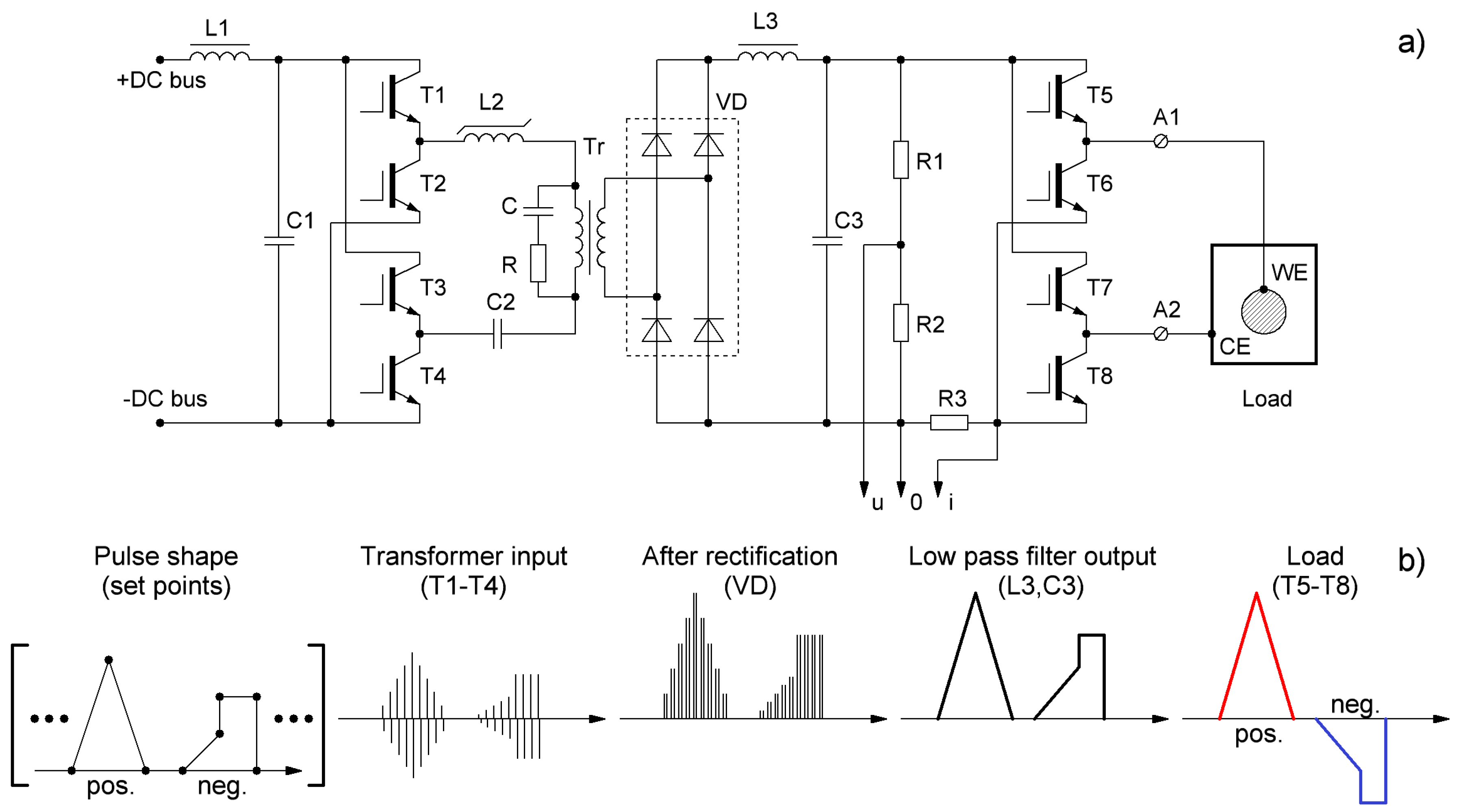
3.3. Prototype Details
- (a) Output voltage (max), V: ±750;
- (b) Output current (max), mA: ±2500;
- (c) Current rise/fall time (max), µs: 100;
- (d) Input: 230 V ±10%, 50 Hz;
- (e) Operation modes: DC, unipolar pulses, bipolar pulses;
- (f) Communication: RS232, USB, WiFi;
- (g) PWM frequency, kHz: 50,000;
- (h) ADC resolution (effective): 12 (10);
- (i) Protections: safety interlock, over current, over voltage, overheating;
- (j) Cooling: active airflow;
- (k) Size/weight (mm/kg): 400 × 270 × 170/5;
- (l) Accuracy (waveform/average): better than 5.0/1.0%;
- (m) Topology: phase shift full bridge.
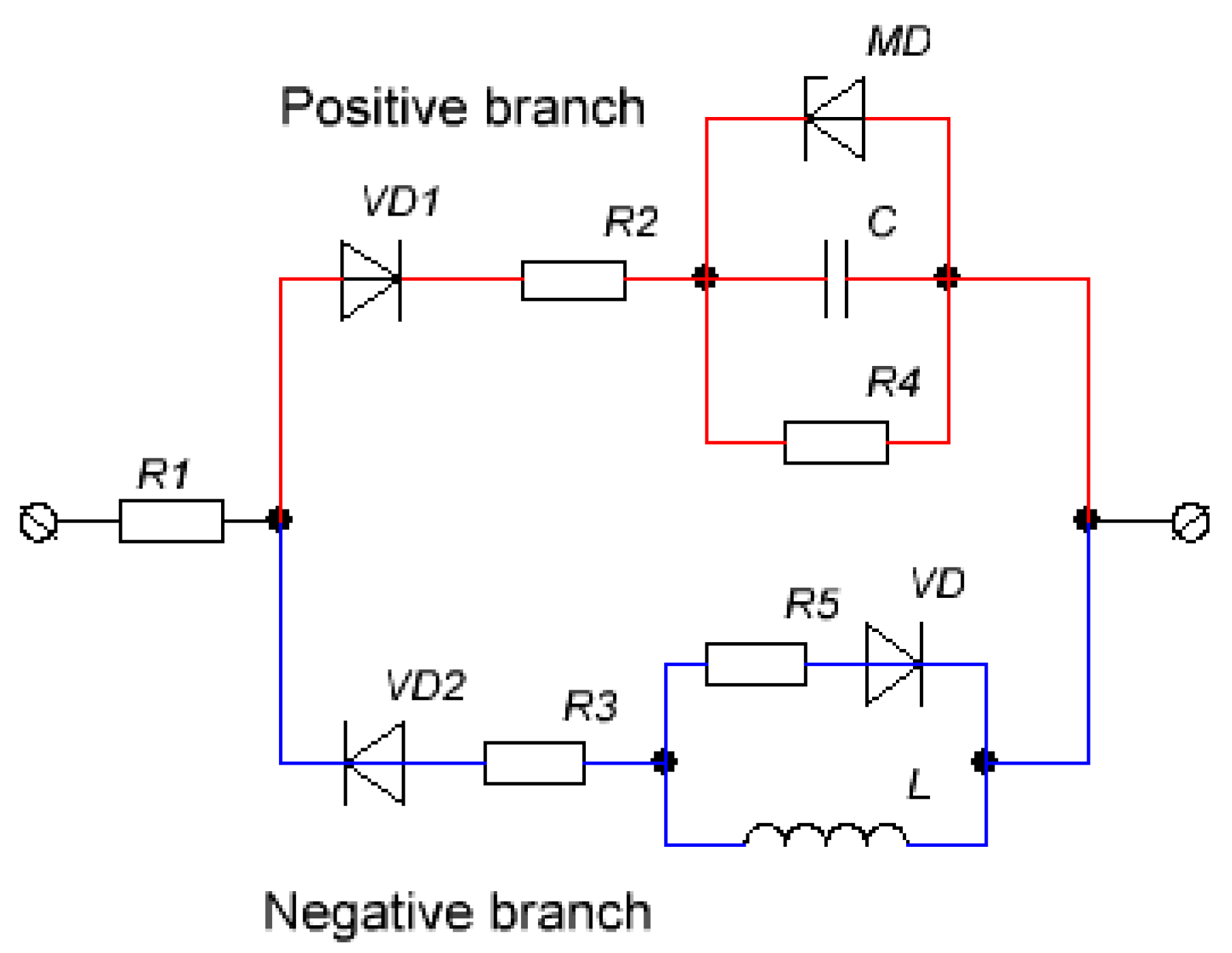
- (a) Power switches: IGBT IKW120N15;
- (b) Isolated drivers: HCNW3120;
- (c) Transformer core: ETD 59;
- (d) Output inductor core: ETD 59 (gap 1.5 mm);
- (e) MCU model: STM32F405;
- (f) Primary safety control: current transformer;
- (g) Secondary monitoring: resistive shunt, resistive voltage divider;
- (h) WiFi module: ESP8266;
- (i) Isolated UART/USB bridge: 6N137 + CH340.
4. Results and Discussion
5. Summary
Funding
Acknowledgments
Conflicts of Interest
References
- Belevantsev, V.; Terleeva, O.; Markov, G.; Shulepko, E.; Slonova, A.; Utkin, V. Micro-plasma electrochemical processes. Prot. Met. Phys. Chem. Surf. 1998, 34, 416–430. [Google Scholar]
- Yerokhin, A.; Nie, X.; Leyland, A.; Matthews, A.; Dowey, S. Plasma electrolysis for surface engineering. Surf. Coat. Technol. 1999, 122, 73–93. [Google Scholar] [CrossRef]
- Walsh, F.; Low, C.; Wood, R.; Stevens, K.; Archer, J.; Poeton, A.; Ryder, A. Plasma electrolytic oxidation (peo) for production of anodised coatings on lightweight metal (al, mg, ti) alloys. Trans. IMF 2009, 87, 122–135. [Google Scholar] [CrossRef]
- Malyshev, V.N. Modification of friction knots work surfaces on the basis of micro arc oxidation method. Int. J. Sci. Res. Sci. Eng. Technol. 2016, 2, 464–480. [Google Scholar]
- Alnaqi, A.A.; Kosarieh, S.; Barton, D.C.; Brooks, P.C.; Shrestha, S. Material characterisation of lightweight disc brake rotors. J. Mater. Des. Appl. 2018, 232, 555–565. [Google Scholar] [CrossRef]
- Mohedano, M.; Matykina, E.; Arrabal, R.; Mingo, B.; Pardo, A. Peo of pre-anodized al–si alloys: Corrosion properties and influence of sealings. Appl. Surf. Sci. 2015, 346, 57–67. [Google Scholar] [CrossRef]
- Narayanan, T.S.; Park, I.S.; Lee, M.H. Strategies to improve the corrosion resistance of microarc oxidation (mao) coated magnesium alloys for degradable implants: Prospects and challenges. Prog. Mater. Sci. 2014, 60, 1–71. [Google Scholar] [CrossRef]
- Dehnavi, V.; Shoesmith, D.W.; Luan, B.L.; Yari, M.; Liu, X.Y.; Rohani, S. Corrosion properties of plasma electrolytic oxidation coatings on an aluminium alloy–the effect of the PEO process stage. Mater. Chem. Phys. 2015, 161, 49–58. [Google Scholar] [CrossRef]
- Sinebryukhov, S.; Gnedenkov, A.; Mashtalyar, D.; Gnedenkov, S. PEO-coating/substrate interface investigation by localised electrochemical impedance spectroscopy. Surf. Coat. Technol. 2010, 205, 1697–1701. [Google Scholar] [CrossRef]
- Lukiyanchuk, I.; Rudnev, V.; Tyrina, L. Plasma electrolytic oxide layers as promising systems for catalysis. Surf. Coat. Technol. 2016, 307, 1183–1193. [Google Scholar] [CrossRef]
- Ved, M.; Sakhnenko, N.; Karakurkchi, A.; Myrna, T.Y. Functional mixed cobalt and aluminum oxide coatings for environmental safety. Funct. Mater. 2017, 24, 303–310. [Google Scholar] [CrossRef]
- Terleeva, O.; Slonova, A.; Mironov, I.; Rogov, A.; Sharkeev, Y.P. Microplasma synthesis of biocompatible coatings with additions of magnesium, silicon and silver on pure titanium from homogeneous electrolytes. Surf. Coat. Technol. 2016, 307, 1265–1273. [Google Scholar] [CrossRef]
- Rakoch, A.G.; Gladkova, A.G.; Melkonian, K.S. Growth kinetics and morphology of black decorative coating formed on 2024 alloy using plasma electrolytic oxidation. Sci. Res. Their Pract. Appl. Mod. State Ways Dev. 2014, 10, 1–6. (In Russian) [Google Scholar]
- Wang, S.; Liu, P. The technology of preparing green coating by conducting micro-arc oxidation on az91d magnesium alloy. Pol. J. Chem. Technol. 2016, 18, 36–40. [Google Scholar] [CrossRef]
- Wu, X.; Qin, W.; Cui, B.; Jiang, Z.; Lu, W. Black ceramic thermal control coating prepared by microarc oxidation. Int. J. Appl. Ceram. Technol. 2007, 4, 269–275. [Google Scholar] [CrossRef]
- Curran, J.; Kalkancı, H.; Magurova, Y.; Clyne, T. Mullite-rich plasma electrolytic oxide coatings for thermal barrier applications. Surf. Coat. Technol. 2007, 201, 8683–8687. [Google Scholar] [CrossRef]
- Shashkov, P.; Khomutov, G.; Yerokhin, A.; Usov, S. Insulated Metal Substrate. U.S. Patent 9,551,082, 24 January 2017. [Google Scholar]
- Stojadinovic, S.; Vasilic, R.; Petkovic, M.; Nedic, Z.; Kasalica, B.; Belca, I.; Zekovic, L. Luminescence properties of oxide films formed by anodization of aluminum in 12-tungstophosphoric acid. Electrochim. Acta 2010, 55, 3857–3863. [Google Scholar] [CrossRef]
- Wang, L.; Zhou, J.; Liang, J.; Chen, J. Thermal control coatings on magnesium alloys prepared by plasma electrolytic oxidation. Appl. Surf. Sci. 2013, 280, 151–155. [Google Scholar] [CrossRef]
- Rudnev, V.; Ustinov, A.Y.; Lukiyanchuk, I.; Kharitonskii, P.; Frolov, A.; Morozova, V.; Tkachenko, I.; Sergienko, V. Magnetic Properties of Plasma Electrolytic Iron-containing Oxide Coatings on Aluminum. Dokl. Phys. Chem. 2009, 428, 189–192. [Google Scholar] [CrossRef]
- Baranova, T.; Chubenko, A.; Ryabikov, A.; Mamaev, A.; Mamaeva, V.; Beletskaya, E.Y. Microarc synthesis of nanostructured radiation-absorbing coatings on aluminum and titanium surfaces. Mater. Sci. Eng. 2017, 286, 012037. [Google Scholar] [CrossRef]
- Martin, J.; Nominé, A.; Brochard, F.; Briançon, J.-L.; Noël, C.; Belmonte, T.; Czerwiec, T.; Henrion, G. Delay in micro-discharges appearance during PEO of Al: Evidence of a mechanism of charge accumulation at the electrolyte/oxide interface. Appl. Surf. Sci. 2017, 410, 29–41. [Google Scholar] [CrossRef]
- Zhang, X.; Tian, X.; Yang, S.; Gong, C.; Fu, R.; Chu, P. Low energy-consumption plasma electrolytic oxidation based on grid cathode. Rev. Sci. Instrum. 2010, 81, 103504. [Google Scholar] [CrossRef] [PubMed]
- Matykina, E.; Arrabal, R.; Mohamed, A.; Skeldon, P.; Thompson, G. Plasma electrolytic oxidation of pre-anodized aluminium. Corros. Sci. 2009, 51, 2897–2905. [Google Scholar] [CrossRef]
- Parfenov, E.; Yerokhin, A.; Nevyantseva, R.; Gorbatkov, M.; Liang, C.-J.; Matthews, A. Towards smart electrolytic plasma technologies: An overview of methodological approaches to process modelling. Surf. Coat. Technol. 2015, 269, 2–22. [Google Scholar] [CrossRef]
- Clyne, T.W.; Troughton, S.C. A review of recent work on discharge characteristics during plasma electrolytic oxidation of various metals. Int. Mater. Rev. 2019, 64, 127–162. [Google Scholar] [CrossRef]
- Dehnavi, V.; Binns, W.; Noël, J.; Shoesmith, D.; Luan, B. Growth behaviour of low-energy plasma electrolytic oxidation coatings on a magnesium alloy. J. Magnes. Alloys 2018, 6, 229–237. [Google Scholar] [CrossRef]
- Vladimirovich Timoshenko, A.; Vladimirovna Magurova, Y. Application of oxide coatings to metals in electrolyte solutions by microplasma methods. Rev Met. Madr. 2000, 36, 323–330. [Google Scholar] [CrossRef]
- Apelfeld, A.; Borisov, A.; Krit, B.; Ludin, V.; Souminov, I. Soft-hardware control and monitoring system of microarc oxidation installations. In Proceedings of the 5th International Conference on MMT Mathematical Modeling and Computer Simulation Material Technologies, Ariel, Israel, 8–12 September 2008; p. 4. [Google Scholar]
- Markov, G.A.; Shulepko, E.K.; Terleeva, O.P.; Kirillov, V.; Fedorov, V.A.; Kan, A.G.; Maksutov, R.A.; Glazunov, V.N. Device for Convertion of Alternating Voltage into the Asymmetric Alternating One. US Patent 1,339,818, 1987. [Google Scholar]
- Samsonov, V.; Hiterer, M. Process for Coating Metals. U.S. Patent 5,616,229, 1 April 1997. [Google Scholar]
- Patel, J.L.; Saka, N. Method for Forming Ceramic Coatings by Micro-Arc Oxidation of Reactive Metals. U.S. Patent 6,197,178, 6 March 2001. [Google Scholar]
- Sun, J.; Qian, W.; Qu, W.; Hui, S. Pulsed Power Supply for Plasma Electrolytic Deposition and Other Processes. U.S. Patent 9,018,802, 8 April 2015. [Google Scholar]
- Chen, M.; Ma, Y.; Hao, Y. Local arc discharge mechanism and requirements of power supply in micro-arc oxidation of magnesium alloy. Front. Mech. Eng. China 2010, 5, 98–105. [Google Scholar] [CrossRef]
- Krainyukov, A.; Kutev, V. Employment of igbt-transistors for bipolar impulsed micro-arc oxidation. Transp. Telecommun. J. 2015, 16, 217–223. [Google Scholar] [CrossRef]
- Chen, H.; Wu, H.; Ma, Y.; Zhang, L.; Li, Z. Research and development of bipolar microarc electrodeposition power supply system. Adv. Technol. Electr. Eng. Energy 2013, 32, 105–109. [Google Scholar]
- Bolshenko, A.V.; Pavlenko, A.V.; Puzin, V.S.; Panenko, I. Power supplies for microarc oxidation devices. Life Sci. J. 2014, 11, 263–268. [Google Scholar]
- Li, Y.; Wu, H.; Wang, J.; Chen, G.; Yu, S. Microarc oxidation power supply based on automatically control. In Proceedings of the 2011 3rd International Conference on Advanced Computer Control (ICACC), Harbin, China, 18–20 January 2011; pp. 79–82. [Google Scholar] [CrossRef]
- Beauvir, J. Oxidizing Electrolytic Method for Obtaining a Ceramic Coating at the Surface of a Metal. U.S. Patent 2,002,112,962, 22 April 2002. [Google Scholar]
- Chen, G.; Zhong, Y.; Sun, Q.; Bai, L. An asymmetryc bipolar pulse circuit based on coupled inductor. Trans. China Electrotech. Soc. 2017, 32, 2–8. [Google Scholar]
- Rogov, A.B. Device for Plasma Electrolytic Oxidation of Valve Metals and Alloys Thereof. RU Patent 2,584,058, 20 May 2016. [Google Scholar]
- Zeng, M.; Chen, X.; Cao, B. Micro-arc oxidation inverter power supply based on the limited bipolar soft-switch control method. Chin. J. Mech. Eng. 2009, 22, 390–394. [Google Scholar] [CrossRef]
- Nomine, A.; Troughton, S.; Nomine, A.; Henrion, G.; Clyne, T.W. High speed video evidence for localised discharge cascades during plasma electrolytic oxidation. Surf. Coat. Technol. 2015, 269, 125–130. [Google Scholar] [CrossRef]
- Nomine, A.; Martin, J.; Noel, C.; Henrion, G.; Belmonte, T.; Bardin, I.; Kovalev, V.; Rakoch, A. The evidence of cathodic micro-discharges during plasma electrolytic oxidation process. Appl. Phys. Lett. 2014, 104, 081603. [Google Scholar] [CrossRef]
- Dunleavy, C.; Curran, J.; Clyne, T. Time dependent statistics of plasma discharge parameters during bulk AC plasma electrolytic oxidation of aluminium. Appl. Surf. Sci. 2013, 268, 397–409. [Google Scholar] [CrossRef]
- Parfenov, E.; Yerokhin, A.; Matthews, A. Frequency response studies for the plasma electrolytic oxidation process. Surf. Coat. Technol. 2007, 201, 8661–8670. [Google Scholar] [CrossRef]
- Yerokhin, A.; Parfenov, E.V.; Matthews, A. Frequency response method for modelling of plasma lectrolytic oxidation processes. In Proceedings of the MMT 2008, Ariel, Israel, 8–12 September 2008; pp. 4–18. [Google Scholar]
- Parfenov, E.; Yerokhin, A.; Matthews, A. Impedance spectroscopy characterisation of peo process and coatings on aluminium. Thin Solid Films 2007, 516, 428–432. [Google Scholar] [CrossRef]
- Gao, Y.; Yerokhin, A.; Parfenov, E.; Matthews, A. Application of voltage pulse transient analysis during plasma electrolytic oxidation for assessment of characteristics and corrosion behaviour of ca-and p-containing coatings on magnesium. Electrochim. Acta 2014, 149, 218–230. [Google Scholar] [CrossRef]
- Fatkullin, A.R.; Parfenov, E.V.; Yerokhin, A. Equivalent circuit modelling for pulsed bipolar plasma electrolytic oxidation process. Int. J. Inf. Electron. Eng. 2015, 5, 63–67. [Google Scholar] [CrossRef]
- Fatkullin, A.R.; Parfenov, E.V.; Yerokhin, A.; Lazarev, D.M.; Matthews, A. Effect of positive and negative pulse voltages on surface properties and equivalent circuit of the plasma electrolytic oxidation process. Surf. Coat. Technol. 2015, 284, 427–437. [Google Scholar] [CrossRef]
- Yang, K.; Cao, B. Electrical characteristics identification of dielectric film breakdown during plasma electrolytic oxidation process. Mater. Lett. 2015, 143, 177–180. [Google Scholar] [CrossRef]
- Heinz, A. Electrolytic Converter for the Transformation of Alternating Currents into Continuous Currents. U.S. Patent 1,097,801, 26 May 1914. [Google Scholar]
- Güntherschulze, A.; Betz, H. Neue untersuchungen über die elektrolytische ventilwirkung. Zeitschrift für Physik 1932, 73, 586–601. [Google Scholar] [CrossRef]
- Sobolev, A.; Kossenko, A.; Zinigrad, M.; Borodianskiy, K. Comparison of plasma electrolytic oxidation coatings on al alloy created in aqueous solution and molten salt electrolytes. Surf. Coat. Technol. 2018, 344, 590–595. [Google Scholar] [CrossRef]
- Rogov, A.; Shayapov, V. The role of cathodic current in peo of aluminum: Influence of cationic electrolyte composition on the transient current-voltage curves and the discharges optical emission spectra. Appl. Surf. Sci. 2017, 394, 323–332. [Google Scholar] [CrossRef]
- Rogov, A.B.; Yerokhin, A.; Matthews, A. The role of cathodic current in plasma electrolytic oxidation of aluminum: Phenomenological concepts of the “soft sparking” mode. Langmuir 2017, 33, 11059–11069. [Google Scholar] [CrossRef] [PubMed]
- Rogov, A.B.; Yerokhin, A.; Matthews, A. The role of cathodic current in plasma electrolytic oxidation of aluminium: Current density ‘scanning waves’ on complex-shape substrates. J. Phys. Appl. Phys. 2018, 51, 405303. [Google Scholar] [CrossRef]
- Gębarowski, W.; Pietrzyk, S. Growth characteristics of the oxide layer on aluminium in the process of plasma electrolytic oxidation. Arch. Metall. Mater. 2014, 59, 407–411. [Google Scholar] [CrossRef]
- Wang, J.-H.; Du, M.-H.; Han, F.-Z.; Yang, J. Effects of the ratio of anodic and cathodic currents on the characteristics of micro-arc oxidation ceramic coatings on al alloys. Appl. Surf. Sci. 2014, 292, 658–664. [Google Scholar] [CrossRef]
- Xiang, N.; Song, R.-G.; Zhuang, J.-J.; Song, R.-X.; Lu, X.-Y.; Su, X.-P. Effects of current density on microstructure and properties of plasma electrolytic oxidation ceramic coatings formed on 6063 aluminum alloy. Trans. Nonferr. Met. Soc. China 2016, 26, 806–813. [Google Scholar] [CrossRef]


© 2019 by the author. Licensee MDPI, Basel, Switzerland. This article is an open access article distributed under the terms and conditions of the Creative Commons Attribution (CC BY) license (http://creativecommons.org/licenses/by/4.0/).
Share and Cite
Rogov, A.B. Smart Arbitrary Waveform Generator with Digital Feedback Control for High-Voltage Electrochemistry. Instruments 2019, 3, 13. https://doi.org/10.3390/instruments3010013
Rogov AB. Smart Arbitrary Waveform Generator with Digital Feedback Control for High-Voltage Electrochemistry. Instruments. 2019; 3(1):13. https://doi.org/10.3390/instruments3010013
Chicago/Turabian StyleRogov, Aleksey B. 2019. "Smart Arbitrary Waveform Generator with Digital Feedback Control for High-Voltage Electrochemistry" Instruments 3, no. 1: 13. https://doi.org/10.3390/instruments3010013