Article

Tunable Photonic Band Gaps in Two-Dimensional Bravais–Moiré Photonic Crystal Composed of High-Tc Superconductors

by
Hernán A. Gómez-Urrea
1,*,
José G. Cardona
1,
Miguel E. Mora-Ramos
2,* and
Carlos A. Duque
3
1
Facultad de Ciencias Básicas, Universidad de Medellín, Medellín 050026, Colombia
2
Centro de Investigación en Ciencias-IICBA, Universidad Autónoma del Estado de Morelos, Cuernavaca CP 62209, Morelos, Mexico
3
Grupo de Materia Condensada-UdeA, Instituto de Física, Facultad de Ciencias Exactas y Naturales, Universidad de Antioquia UdeA, Calle 70 No. 52-21, Medellín 050010, Colombia
*
Authors to whom correspondence should be addressed.
Condens. Matter 2023, 8(2), 51; https://doi.org/10.3390/condmat8020051
Submission received: 10 April 2023 / Revised: 26 May 2023 / Accepted: 30 May 2023 / Published: 2 June 2023
(This article belongs to the Special Issue Physics of Light-Matter Coupling in Nanostructures)

Abstract

:
In this study, we perform a theoretical study of light propagation properties in two-dimensional square photonic crystals (PCs) following Bravais–Moiré (BM) patterns composed of copper oxide high-temperature superconductors (HTSCs). The BM PCs are made of cylindrical cores formed from the combination of two square Bravais lattices. The Moiré pattern forms due to a commensurable rotation of one of these lattices with respect to the other. The dielectric function of the superconducting material is modeled by the two-fluid Gorter–Casimir theory. We report on the corresponding gap, the mapping as a function of the radius of dielectric cores, as well as the dispersion relations of TM modes for BM PCs and for the waveguide system built of defect lines within such a crystal. The BM PCs were composed of copper oxide HTSCs, which exhibit large tunability in terms of temperature.

1. Introduction

Photonic crystals (PCs) are structures whose refractive index varies periodically in space. By creating a contrast in the refractive indices of the materials that compose the structure, it is possible to obtain photonic band gaps (PBGs) for electromagnetic radiation. This implies the absence of transmission for signals with frequencies within a given interval of values. Such a property is highly useful in applications involving optical devices [1,2,3,4,5,6,7,8,9,10,11,12,13,14,15,16,17,18,19,20]. For these applications, it is essential to tune the properties of PBGs and to obtain the widest possible band gaps. Typically, the contrast between refractive indices is achieved by changing the filling fraction (the ratio between the radius of the cylinders and the lattice constant) and the type of lattice. Once the geometry is determined, PBGs can only be adjusted by changing the constituent materials. In this sense, using tunable materials in the design and fabrication of PCs allows one to adjust the optical properties with high flexibility. Tunable materials include metals and semiconductors, which are highly dispersive and whose band structure depends strongly on plasma frequencies [21,22]. However, these types of materials have some drawbacks. For example, metals exhibit inherent losses, which are caused by the extinction coefficient. To overcome these problems, a variety of unconventional materials have been used, such as superconductors [1,2,3,4,5,6,7,8,9,10,11,12,13,14,15,16,17,18,19,20]. In superconductors, optical properties are strongly influenced by temperature and magnetic fields. Compared to PCs with metallic components, superconductors have the advantage of low loss and adjustable permittivity. In the superconducting state, the electromagnetic wave can only propagate within the London penetration depth of the materials. In the normal state, the London penetration depth becomes infinite, and the electromagnetic wave can propagate in the material without limitations [7].
High critical-temperature superconductors (HTSCs) based on cuprates exhibit transition temperatures (30–150 [K]) that make them suitable for applications as they show superconductivity under liquid nitrogen conditions [7]. Within the study of the properties of 2D PCs based on cuprates, W. M. Lee and P. M. Hui [23] studied the band structure in 2D PCs composed of dielectric cylinders in a CU-based HTSC background. Among their results, the authors report the appearance of almost flat bands; a finding that is very convenient for slow light applications that, from the optical point of view, require the integration of device components, as well as the control of light signals in the time domain [24]. Takeda and Yoshino [7] considered a 2D PC with copper oxide HTSC cylinders in an air background. They reported that the band structure was highly tunable in terms of temperature and magnetic field. Barvestani et al. analyzed the guided modes in a 2D PC with aluminum cylinders in an air background, in which a defect line was obtained by replacing the aluminum of the cylinders in the line with a CU-based HTSC. The results show that the sensitivity of guided mode frequencies depends considerably on the size of the HTSC core compared to those using dielectrics, and the frequency of the modes can be adjusted as a function of temperature.
PC waveguides are relevant to optical applications due to their radiation guiding properties. They are usually constructed by creating a line of defects within the periodic PC lattice. Another way to construct them involves building a chain of point defects or strongly coupled cavities, known as coupled resonator optical waveguides (CROWs) [25]. In previous works involving CROWs with multiple cores in the unit cell (UC), low group velocities have been found in the guided modes [23,26]. Additionally, isotropy in the PBGs has been reported in those systems. This means that the PBG is independent of the direction of electromagnetic propagation. Such a feature favors the appearance of wider PBGs [27,28,29], and it indicates that this type of multi-core PC unit cell can be used in applications involving slow light.
Bravais–Moiré (BM) lattices are a particular case of systems with multiple cores in their unit cell (UC). This type of system can be seen as the superposition of two or more Bravais lattices, which are rotated with respect to each other by a commensurate angle, providing an additional parameter for tuning the optical properties of the considered systems [26]. Previous works on these systems have reported wide PBGs, isotropy in the band structure, and radiation localization properties in the structure [26,30,31,32,33,34]. Additionally, guided modes have been considered [26,35,36,37] in both conventional PC waveguides [35,37] and CROWs [26]. These works have shown how BM networks favor the appearance of wide PBGs and the low group velocity of guided modes.
In 2D PCs with BM lattices, the analysis of plasmonic systems has been considered—particularly the scattering of surface plasmons—from an experimental point of view [30,31,32]. Additionally, the photonic properties of dielectric-based BM PCs have also been reported [38,39]. To the best of our knowledge, the study of guided modes in CROWs with BM networks in Cu-based HTSCs has not yet been considered.
In this work, we investigate the features of light propagation in 2D square PCs following Bravais-Moiré (BM) patterns. Structures are assumed to be composed of copper oxide high-temperature superconductors (HTSCs). The BM PCs are made of cylindrical cores formed from the combination of two square Bravais lattices, such as the one considered in [26]. A waveguide is built into the system by means of defect lines within the structure. We report on the corresponding gap mapping as a function of the dielectric core radius. In addition, the calculated dispersion relations for TM and waveguide modes, as well as the group velocity of such localized modes are presented and discussed. It is shown that BM PCs that are composed of copper oxide HTSCs exhibit noticeable temperature-related tunability. In addition, it is found that a significant reduction in group velocity is achieved for guided modes compared to PC systems based on dielectrics.

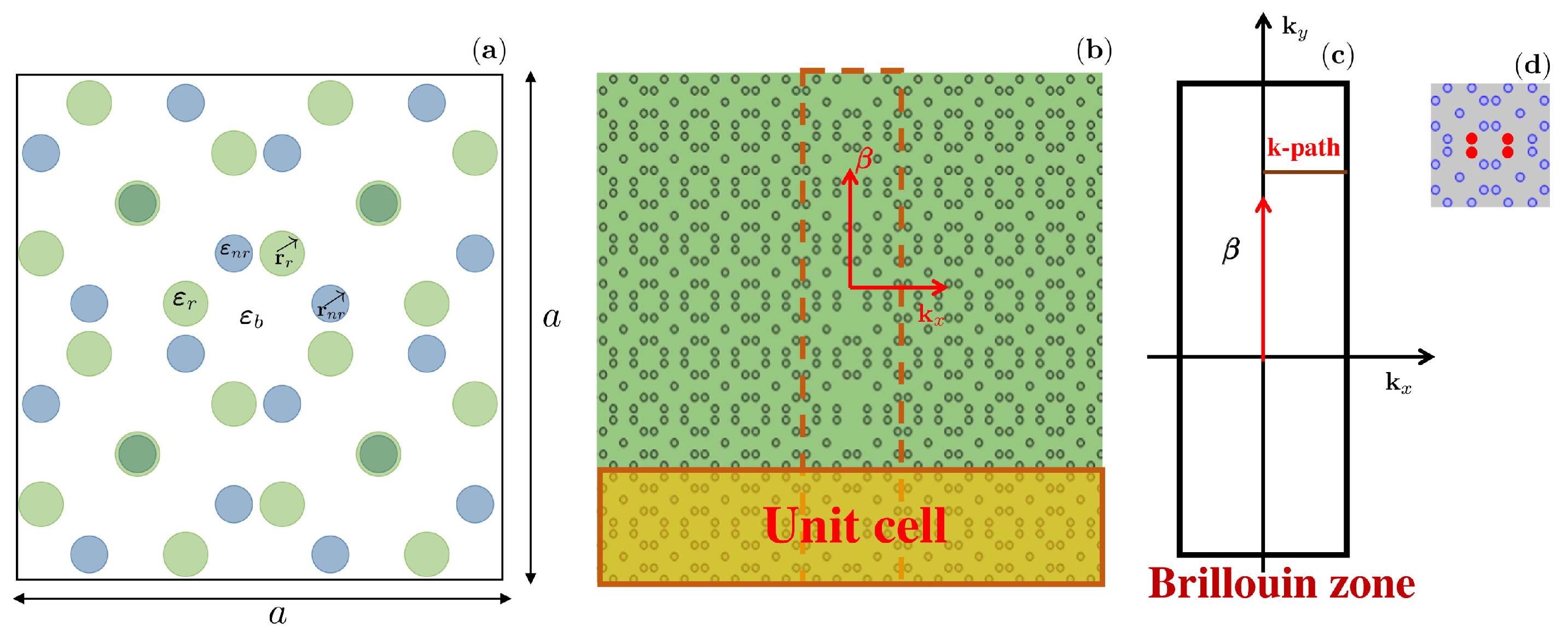
2. Description of the System

In this work, we focus on the analysis of guided modes in BM networks. We consider the special case presented in ref. [26], where a commensurate rotation of ϕ = 53 . 13 with r = 3 ,   s = 1 (BM-R3S1, according to the notation presented in [26]) is considered. Figure 1a shows the unit cell (UC) corresponding to this structure. In this case, the UC is composed of 40 dielectric cores that have a circular cross section (blue circles in the figure), of which 20 correspond to the square Bravais lattice without rotation (with radius r n r and dielectric permittivity ε n r ), and 20 dielectric cores with circular cross section (green circles in the figure), which correspond to the rotated Bravais lattice (all with radius r r and dielectric permittivity ε r ). This rotated—at a commensurate angle—square lattice was superimposed over the first one to form the BM pattern. In the construction, a is the lattice constant and ε b is the dielectric permittivity of the background. This construction is further detailed in refs. [26,33,34].
To design CROWs, the structure is optimized in such a way that the PBGs are as wide as possible to ensure that the guided modes appearing in the PBG region, after introducing defects, are located in the central part of the PBG and that they do not interact with modes in the continuum [40]. For this analysis, a scan is performed over the filling fraction, and the band structure is calculated in the UC of Figure 1a. The parameters for the UC that optimize the PBG are used to construct the CROW. The CROW considered in this work is shown in Figure 1b. It is constructed by removing some cylinders from the UC. Particularly, in Figure 1d, the cylinders that are removed are shown in red. For the analysis of the dispersion relations in the CROW, it must be considered that the waveguide is not a perfectly periodic structure in both directions, as can be seen in the UC marked in yellow in Figure 1b. However, it is still periodic in the waveguide direction. For the calculation, an infinite translation of a part of the PC containing the defect was assumed. Thus, the UC is larger and contains several periods (see the yellow box in Figure 1b). Since the signal propagates in the waveguide direction, radiation confinement occurs in the transverse direction. Hence, the wave vector is separated into two components: the first one is perpendicular to the direction of wave propagation and is connected to the dispersion relation of the waveguide, and the second one, which is in the waveguide direction, is known as the propagation constant and is designated as β [40]. Figure 1c shows the Brillouin zone of the waveguide.

2.1. Theoretical Framework

Maxwell equations govern the propagation of electromagnetic waves in the PC. Through their solutions, we shall be able to investigate the photonic properties of the system of interest. For a 2D medium, electric and magnetic fields can be written as linear combinations of transverse electric (TE) and transverse magnetic (TM) components. Here, we restrict ourselves to dealing with TM modes. Accordingly, the sourceless Maxwell–Helmholtz equation for the magnetic field reads:
H z ( r ) ε r ( r ) k 0 2 H z ( r ) = 0 ,
where H z ( r ) is the field’s z-component at the position r . Time-harmonic electric and magnetic fields come from the solution of Equation (1), according to the following:
H ( r , t ) = H z ( r ) e i ω t z ^
E ( r , t ) = i k 0 ε ( r ) × H ( r , t ) .
PC periodicity is used in order to obtain the corresponding dispersion relations. It comes from the application of the Bloch theorem at the borders of the unit cell. When the electric (magnetic) field propagates between the PC points separated by a lattice vector, R , the only effect on the field is the change in phase given by the following:
H z ( r + R ) = H z ( r ) e i k · R ,
Here, R is a photonic lattice vector and k is the signal wavevector.
In addition, the dielectric function of the superconductor material (SC) was modeled by the two-fluid model to describe the electrodynamics of the superconductor cores at nonzero temperatures [2,10]:
ε s c ( ω ) = ε 1 ω s p 2 ω 2 ω n p 2 ω ( ω + i γ )
ε is the high-frequency permittivity of HTSC and γ is a damping term. ω s p = c / ( λ L ( T ) ε ) and ω n p = ( n n e 2 / m ε 0 ε ) 1 / 2 are the plasma frequencies of superconducting and normal conducting electrons, respectively. Here, λ L ( T ) = ( m / μ 0 n s e 2 ) 1 / 2 is the London penetration depth, and the dependency of it on the temperature from the Gorter-Casimir model can be written for HTSC as per the following [7]:
λ L ( T ) = λ L ( 0 ) 1 T T c
where c, n n , n s , m, ε 0 , μ 0 , e, and T c are the speed of light in vacum, concentration of normal electrons, concentration of superconductor electrons, the electron mass, permittivity, permeability of vacuum, charge of the electron, and the critical temperature of the superconductor, respectively.

2.2. Simulation Settings

A solution of the wave Equation (1) was accomplished via the finite element method (FEM). The core of FEM consists of mess generation: the partition of geometry into small units of a given shape. Once constructed, dependent variables are approximated by means of known -shape- functions. By inserting this approximation in Equation (1), it is possible to generate a set of algebraic equations, which are suitably solved. Then, the solution of the differential problem is assembled. To carry out our study, we used FEM as implemented in the COMSOL-MULTIPHYSICS licensed software package 5.6 [41]. The description of this tool, including the foundations of FEM, the building of meshes, the discretization of differential equations, optimization, and the convergence criteria can be found in refs. [42,43].

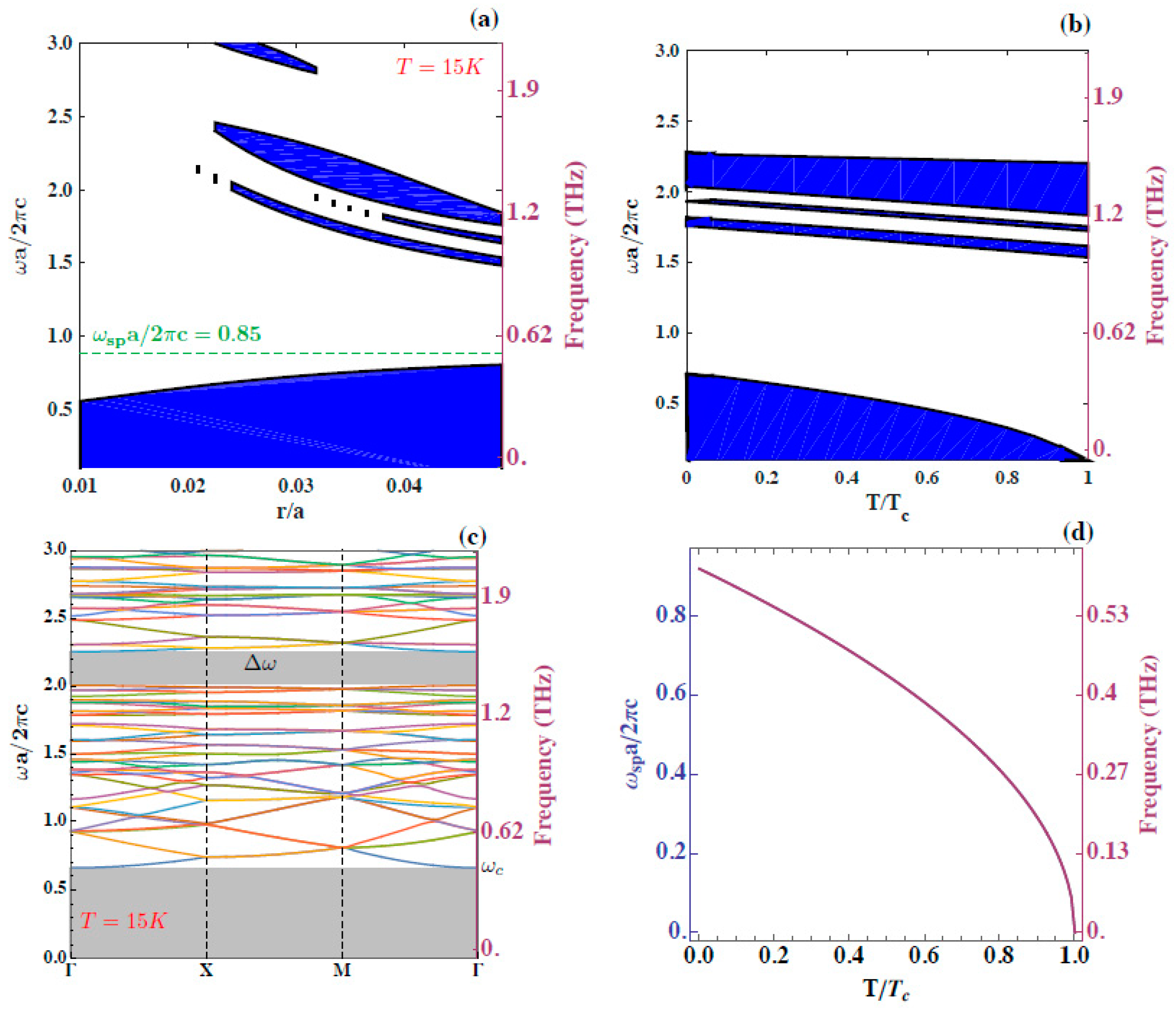
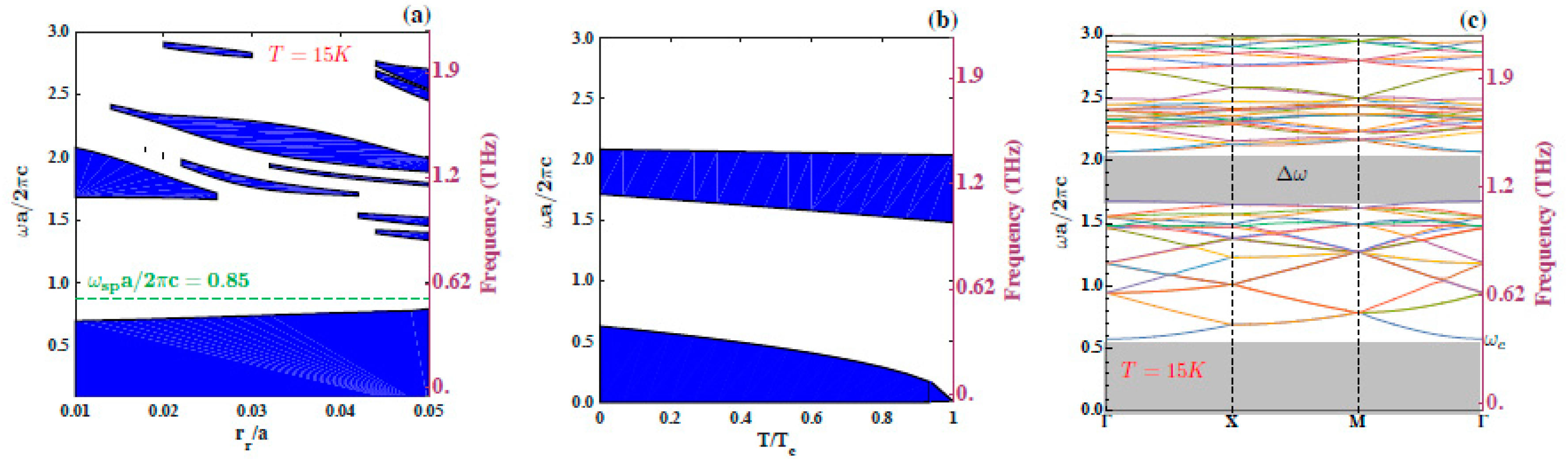
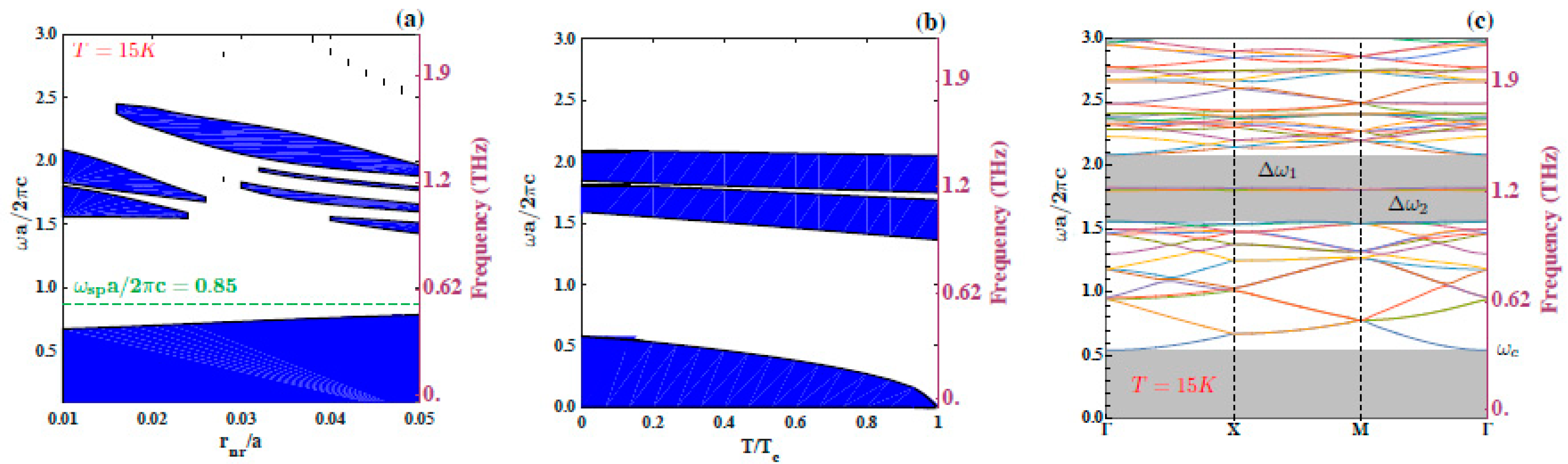
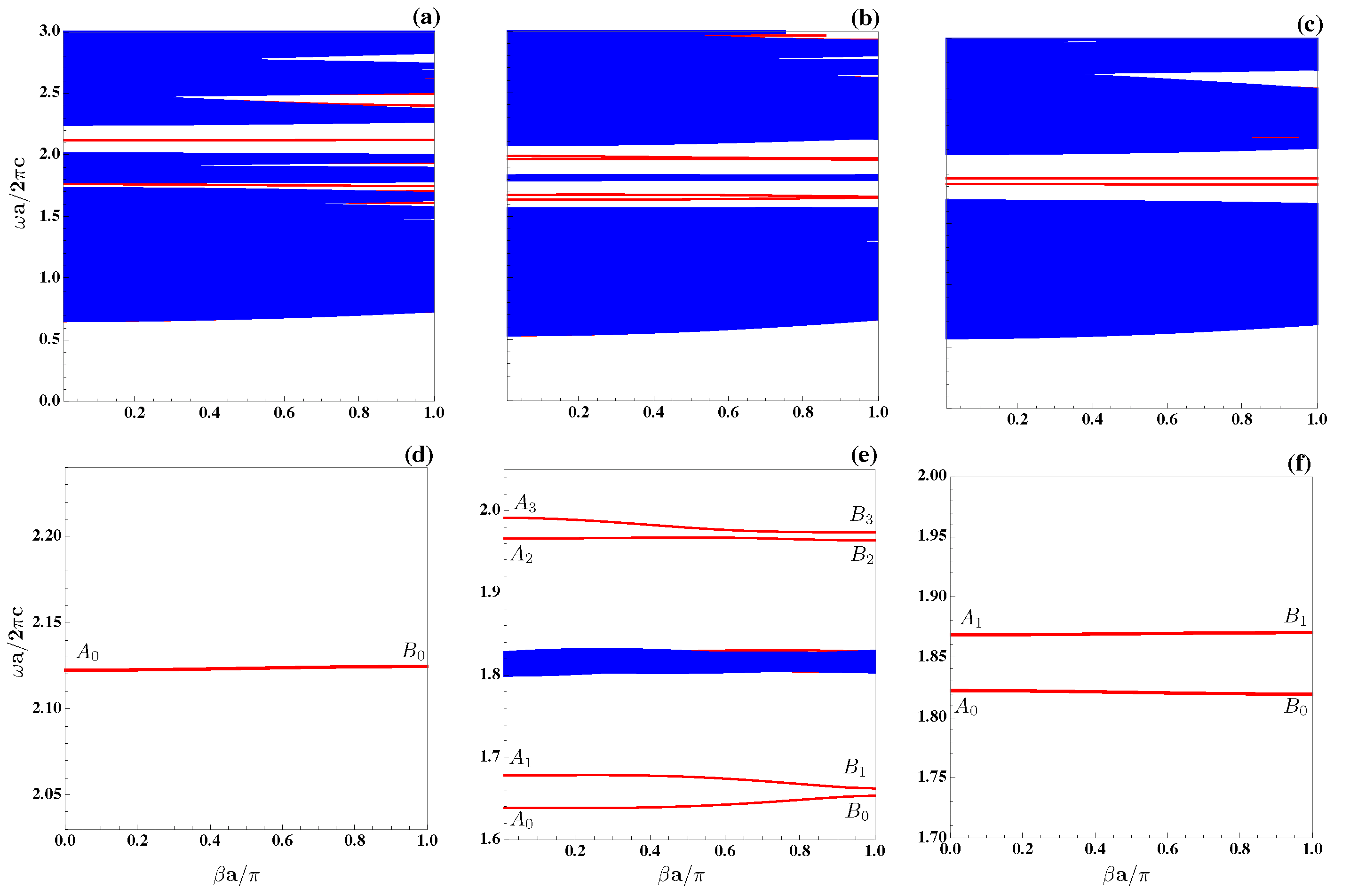
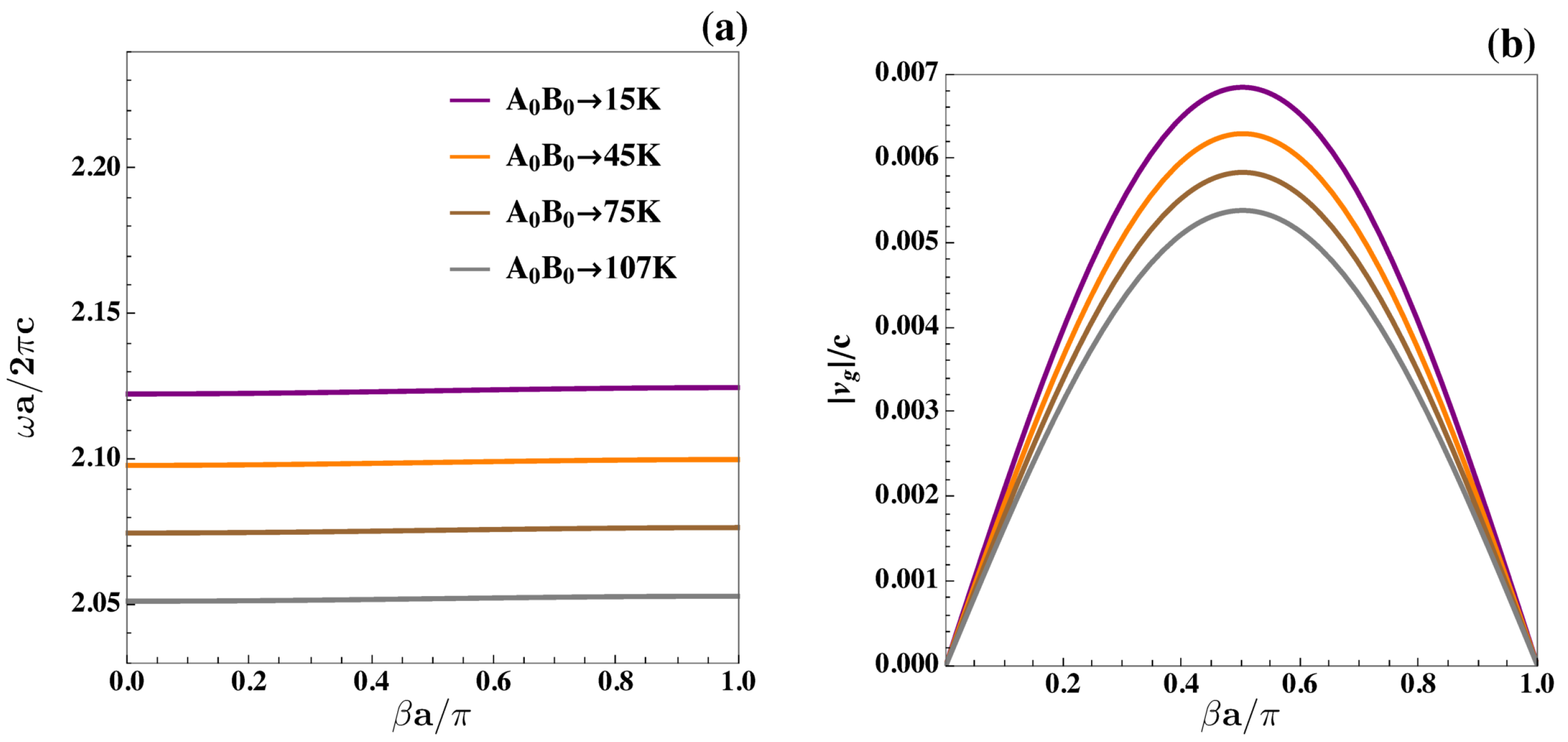
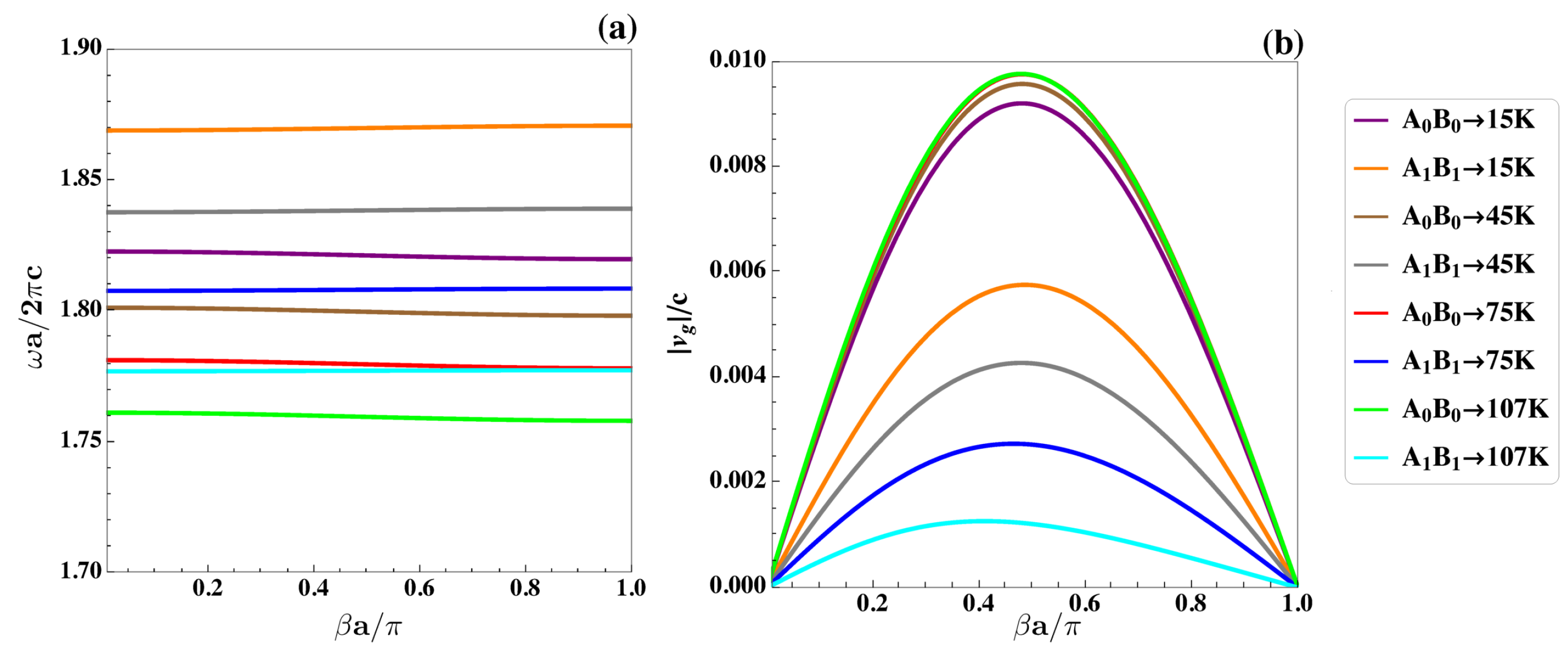
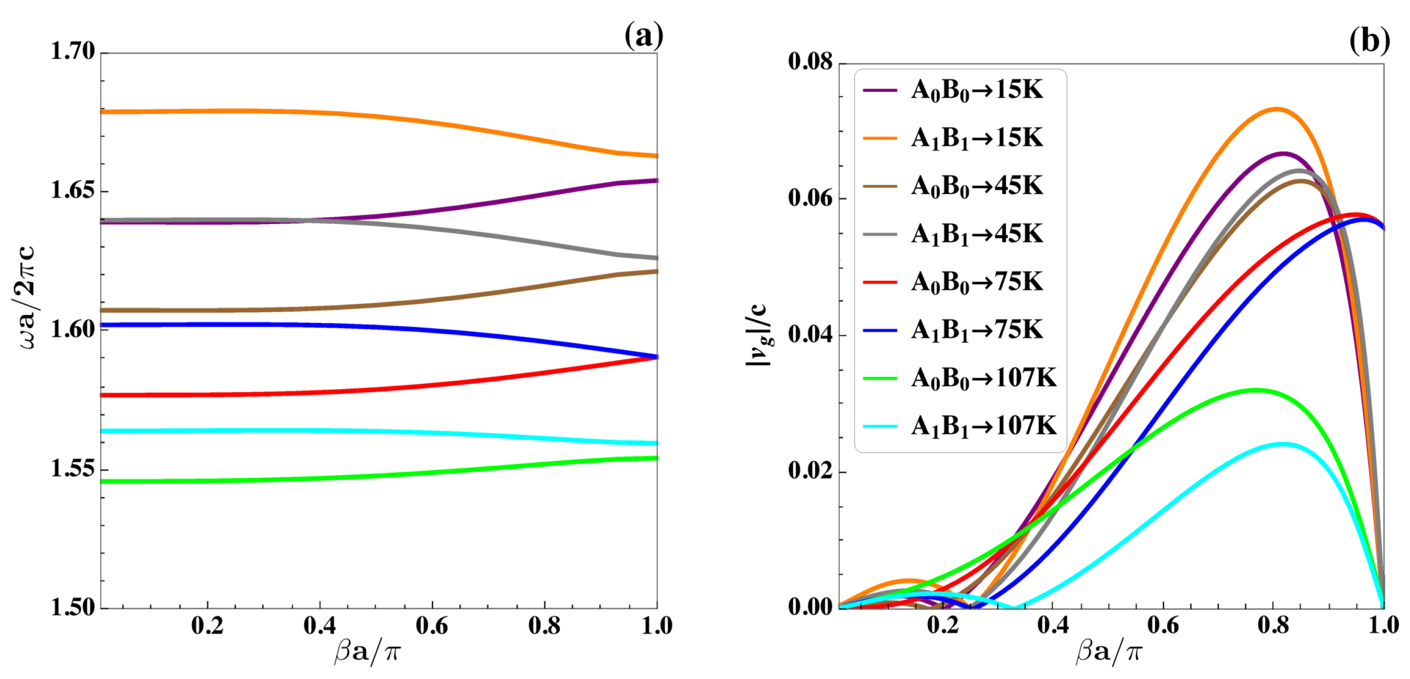
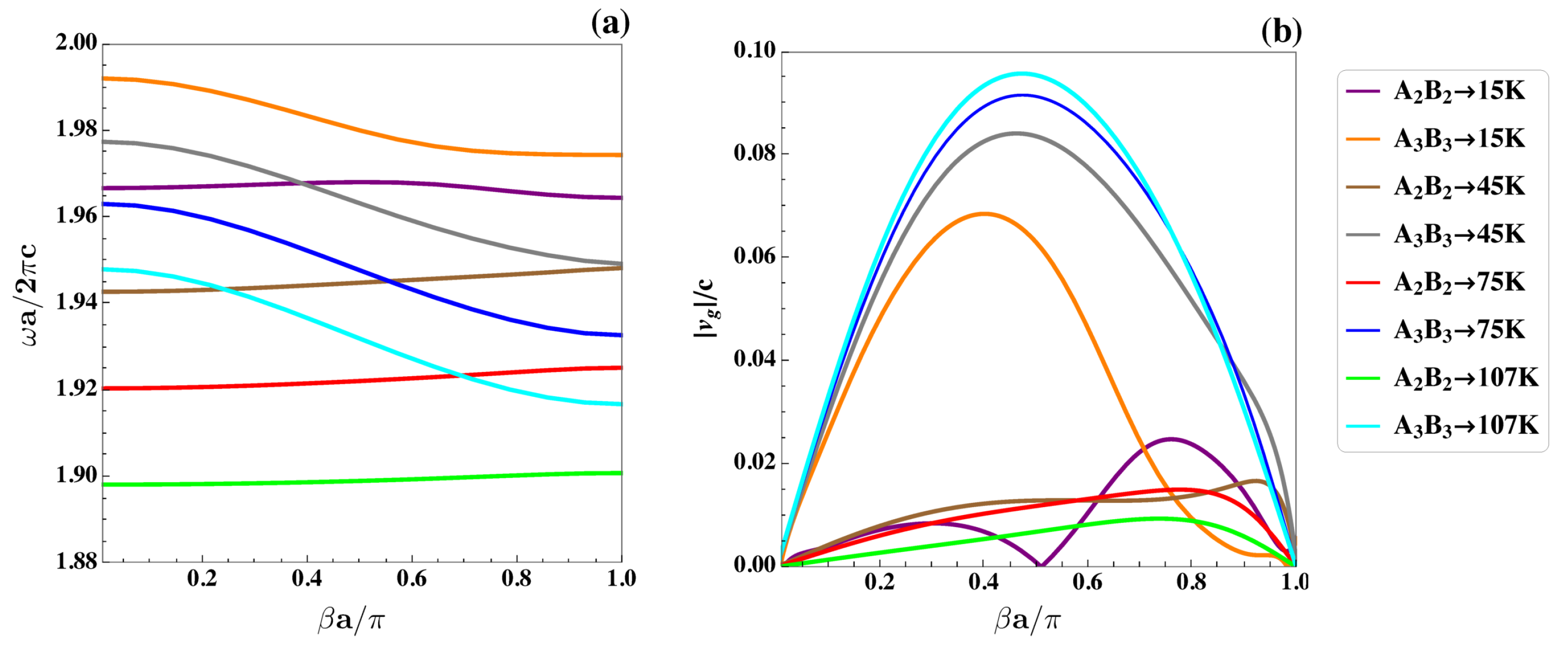
3. Results and Discussion

In the design of the 2D PC considered in this work, the cylindrical cores (both rotated and non-rotated) were made of the SC compound B i 1.85 P b 0.35 S r 2 C a 2 C u 3.1 O y . This compound has a ε = 12 , λ L ( 0 ) = 22.452   μ m and T c = 107 K [7]. Figure 2 shows the calculated PBG mapping for the TM modes in the BM PC, which is schematically depicted in Figure 1. This mapping appears plotted in Figure 2a—for the fixed value of temperature, T = 15 K—as a function of the ratio between the core radius and lattice constant, r / a , which considers that both rotated and unrotated elements have the same radius, r r = r n r = r . Figure 2b contains the mapping as a function of T for the value r / a = 0.0334 = r m , which corresponds to the widest PBG obtained from Figure 2a. In this variation, the widest PBG ( Δ ω = 0.37 ) appears just for T / T c = 1 . The dispersion relation that corresponds to r m and T = 15 K appears in Figure 2c, with the vertical axis in units of ω a / 2 π c . The forbidden regions, represented by the blue fringes in Figure 2a,b, and the lowest gray stripe in Figure 2c correspond to the interval of frequencies below the T-dependent cut-off value, ω c a / 2 π c = 0.67 , at which the effective dielectric function of the structure vanishes. Notice that, as expected, ω c becomes zero when T = T c , but when T is fixed at 15 K, it has a slight increasing rate with r / a . This indicates the effect of geometry on the setting of the overall dielectric response in the unit cell. The second gray stripe highlighted in the dispersion relation is, precisely, the widest PBG, resulting from setting r m at 15 K, ( Δ ω = 0.25 ), which is located between ω a / 2 π c = 2.01 and ω a / 2 π c = 2.26 . It is worth noting that, in this and the following figures showing PBG mappings, the lowest colored stripes just indicate the frequency interval below the cut-off value, for which no propagation of any electromagnetic signal in the system is allowed.
According to Figure 2, due to the chosen design, our working frequency range lies between 0 and 2 THz, which falls within the far-infrared region of the spectrum. As pointed out in refs. [5,7], if the collision frequency γ = 1 / τ for unpaired electrons is much larger than the working frequency, the contribution from the third term in Equation (5) can be neglected, as has already been conducted in previous works [7]. Based on the results presented in ref. [44], the collision time for Bi-based materials can be estimated to be around τ = 1.38 × 10 14 s. This leads to the condition ω 72.5 THz, which is fulfilled without problems within the declared working range. Without the influence of such a term in ε s c ( ω ) , the absorption losses from the normal state subsystem are not relevant in our calculation.
To work within the mentioned frequency range, the lattice constant of the structure will then be chosen to operate in this region of the spectrum; thus, we set a = 0.45 mm. In order to achieve a greater contrast in the refractive indices of the materials in the unit cell, the cylindrical cores are considered in an air background, where ε b = 1.0 . Furthermore, copper oxide HTSCs exhibit strong two-dimensional anisotropy. In this case, to evaluate the TM modes in the two-dimensional photonic crystals considered here, the electric field is considered parallel to the c-axis of the HTSC ( E c ) [7].
In Figure 3a, the results for the gap mapping of TM modes in the considered BM PC, the fixing of unrotated cylinders at r n r / a = 0.0334 , and the varying in the size of the unrotated cores are shown. The remaining parameters are kept with the same values employed to produce Figure 2. One now observes the opening of a main gap for lower frequencies, which widens toward the smallest value of r r / a , thus reaching the maximum Δ ω = 0.39 when r r / a = 0.01 , as depicted in Figure 3c. It is also noticed that the forbidden fringe below the cut-off frequency evolves differently, with a slightly smaller value for the maximum gap configuration when compared with Figure 2c.
Another result related with PBG properties appears from the analysis of gap mapping presented in Figure 4. This time, the calculation has a fixed value of rotated SC cylinders, r r / a = 0.0334 , while the radius of unrotated ones, r n r , changes. As before, the remaining parameters are the same used for Figure 2. The main difference revealed with this particular setup is the appearance of a double PBG for the lowest values of r n r / a . In the case of maximum amplitudes ( r n r / a = 0.01 ), both gaps have almost the same widths, Δ ω 1 = 0.26 and Δ ω 1 = 0.24 (in units of ω a / 2 π c ), and are separated by a narrow interval of ω a / 2 π c = 0.03 .
To summarize the effects of geometry manipulation on the presence and features of PBGs in BM PCs made of high- T c B i 1.85 P b 0.35 S r 2 C a 2 C u 3.1 O y SC, Table 1 contains the compilation of the above-commented results. In accordance, the particular setup shown in the middle row (corresponding to the situation depicted in Figure 3) results in the most suitable setup for PBG enhancement.
Going over to the analysis of waveguide modes in the proposed superconductor BM PC, we keep in mind the design schematically shown in Figure 1b–d. In this sense, the light dispersion relations for the coupled resonator optical modes appearing in waveguides built following such a design, for each of the geometric and thermal configurations detailed in the first column of Table 1, are plotted in Figure 5a–c, respectively. They appear as almost dispersionless horizontal lines (in red color). Corresponding enhanced views of dispersion in the frequency regions around the guide modes are then shown in Figure 5d–f. In this plotting, the blue stripes represent the continuum states. The presence of waveguide modes close to the middle of main PBG intervals—which are quite away from the continuum—indicate a strong spatial localization within the defect line so constructed, and this constitutes a favorable feature.
The flatness of dispersion relations for some of these coupled resonator modes indicates at a significant reduction in the group velocity, v g , of the associated light signals. For that reason, we performed a detailed analysis of this quantity for the different guided modes revealed in order to identify the temperature-dependent slow light properties in the system. In this sense, Figure 6 and Figure 7 contain the analysis of coupled resonator waveguide modes, which vary as a result of the increase in the temperature of the structure from T = 15 K to the T c value. These four figures, respectively, correspond to the guide mode cases depicted in Figure 5d,e (with separate analysis of the modes within the lower (Figure 8) and upper (Figure 9) PBGs) and Figure 5f.
In general, it is possible to observe a trend showing a lowering in the frequency position of the guided modes with an increase in T. In addition, some of those modes showing greater dispersion at low values of the temperature become flatter when it approaches the critical value. However, the influence of the geometrical setup on their group velocities should be more carefully analyzed. In fact, the situations in which there is a single main PBG with either one or two localized modes—that is, the ones observed in Figure 5a,c—display rather symmetric variations of | v g | / c with respect to the center value of the interval for propagation constant values. Such cases are depicted in Figure 6b and Figure 7b. Their respective normalized maximum values (NMVs) for such a quantity are presented for the different temperatures considered in Table 2 and Table 3. From them, it is possible to observe values of the NMVs of group velocity in the order of 10 3 , which decrease as long as T augments toward T c ; in particular, the mode labeled as A 1 B 1 in Figure 5f, is where this stands out. This mode is one of those that reduces its dispersion and becomes flatter with augmenting T. It bears the smallest calculated value for the NMV of group velocity: | v g | / c = 0.0013 (almost three orders of magnitude of reduction from c). As such, it is possible to speak here of a real slow light phenomena.
However, the picture showing the guided modes appearing under the geometrical setup corresponding to Figure 5b,e is significantly different. They are localized within the two close PBGs of almost the same widths that appear in the configuration with a radius of rotated SC cylinders r r / a = 0.0334 and with radius of the rotated ones r n r / a = 0.01 . As already stated, the modes confined within the lower ( A 0 B 0 and A 1 B 1 ) and upper ( A 2 B 2 and A 3 B 3 ) PBGs are analyzed separately in Figure 8 and Figure 9. Here, the NMVs of | v g | / c appear, and they are reported in Table 4 and Table 5, respectively.
By first analyzing the guided modes inside the lower PBG, it is possible to observe their tendency to become largely dispersive for the larger values of the propagation constant, and for them to become very close in frequency. This indicates a possible coupling between them, as noticed in the case of T = 75 K. True, such a dispersive tendency reduces with the increment of T toward the superconductor transition value. This phenomenon is reflected in the group velocity by suppressing any kind of symmetric variation with β , as occurs in the above-discussed cases. In fact, the position of the curve maximum shifts to higher values in the horizontal axis of Figure 8b. From Table 4, one may observe that, once again, increasing temperature leads to a reduction in the NMVs of the group velocity for both modes, whereby the upper one achieved the smaller value. Nonetheless, the achieved values remain in the order of 10 2 , and these results are not better than those discussed in the two previous cases.
With regard to the second (upper) pair of waveguide modes shown in Figure 5b,e, the plots in Figure 9a indicate the already commented shift to smaller frequencies. These are induced by the increment of temperature, as well as due to the trend of the lower one to become dispersionless with T. In contrast, the higher of these two modes keeps a rather strong dispersion. Interestingly, this particular mode, at the time of evolving with the temperature, is located farther away from the other. As a consequence, it was seen that the associated curve of | v g | / c tends to recover the symmetric character with respect to the center of the β region and the group velocity augments, as observed from Table 5 (mode labeled as A 3 B 3 ). On the other hand, the lower of the two waveguide modes under discussion shows a non-symmetric variation of group velocity, which shifts toward the intermediate and higher values of the propagation constant, at which point the greater dispersion occurs. As we have already said, the two modes become closer in that region, and their coupling seems to affect the group velocity of the signal in such a way that | v g | / c curves turn to asymmetry within the region, with a reduction in the NMVs of signal velocity. The only exception for these is what occurred in the picture at T = 45 K. In this case, the A 3 B 3 mode strongly disperses, approaching A 2 B 2 mode at higher values of β . According to Table 5, the MNVs of group velocity remain higher than the values presented for the other two geometrical setups, although the A 2 B 2 mode evolves within small multiples of 10 2 . Thus, one may also talk about the situation of slow light for it within the range of temperature involved.
Previous works on Cu-based HTSC 2D PCs, such as the one reported in refs. [7,45], where simple square lattices of SC cylinders are considered, our system presents better properties for adjusting PBG properties, as can be seen in Figure 2, Figure 3 and Figure 4. This is because, by having multiple cores in the UC, the active component of the SC cores can be changed by the filling fraction with a greater flexibility than in the case of the typical square lattice. In fact, our results show that the band structure is strongly affected when considering geometrical changes, particularly in the radius of the non-rotated cores compared to the rotated ones. Compared with more recent works, such as the one reported in [10], we found that—in addition to the flexibility for adjusting the guided modes as a function of temperature—the guided modes in our system exhibit a low group velocity, which is not observed in the referenced work. As such, it is worth highlighting, at this point, that such low values of normalized group velocities for waveguide signals are obtained with the use of a HTSC as constituent of BM PCs. These are, in some cases, almost an order of magnitude smaller than those calculated for the BM PCs made of dielectric cores [26]. It is also possible to compare with the works that consider CROWs in other designs of lattices with multiple atoms, such as the one reported in [23]. There, the authors consider CROWs in Archimedean-like lattices with dielectric cores, and with report group velocities that are smaller than those reported in usual networks, some even as low as 0.030 times the speed of light in a vacuum. In our work with SC BM PCs, we found velocities as small as 0.0013 times the speed of light in a vacuum, which is three orders of magnitude smaller than the speed of light. This represents a true slow-light behavior, with the additional possibility of adjusting such velocity with temperature, thus indicating the advantage of SC-based photonic structures for slow-light applications.

4. Conclusions

In this work, we have studied the properties of light propagation in a two-dimensional photonic crystal whose unit cell was constructed according a Bravais–Moiré pattern and was composed of high- T c superconducting cylinders. This study also includes the proposal for a design of a line-defect waveguide.In addition, the coupled resonator modes associated to it were also investigated. It was shown that the different geometrical setups arising from the fixation, or the variation of the core cylinder radii, have an impact on the photonic gap mapping of the crystal and also on the appearance and amount of waveguide modes inside such gaps, without a coupling with the continuum.
In addition, the analysis of the group velocity for the guided modes, when considering the variation in the temperature up to the superconductor transition value, allows one to identify particular configurations for which the values of the normalized maximum value of this property reduces to almost three orders of magnitude compared to the vacuum speed of the electromagnetic waves with those frequencies. This fact indicates positive prospects for slow-light applications.

Author Contributions

Authors contributed by performing the indicated activities: conceptualization, H.A.G.-U. and M.E.M.-R.; methodology, H.A.G.-U.; software, J.G.C. and H.A.G.-U.; validation, J.G.C. and H.A.G.-U.; formal analysis, H.A.G.-U. and M.E.M.-R.; writing-review and editing, H.A.G.-U., M.E.M.-R. and C.A.D. All authors have read and agreed to the published version of the manuscript.

Funding

This research was funded by the Mexican CONACYT (grant number A1-S-8218 (MEMR)). CAD is grateful to the Colombian Agencies: CODI-Universidad de Antioquia (Estrategia de Sostenibilidad de la Universidad de Antioquia) and projects “Propiedades magneto-ópticas y óptica no lineal en superredes de Grafeno”, “Estudio de propiedades ópticas en sistemas semiconductores de dimensiones nanoscópicas”, “Propiedades de transporte, espintrónicas y térmicas en el sistema molecular ZincPorfirina”, and “Complejos excitónicos y propiedades de transporte en sistemas nanométricos de semiconductores con simetría axial”, as well as to the Facultad de Ciencias Exactas y Naturales-Universidad de Antioquia (CAD exclusive dedication project 2022–2023).

Data Availability Statement

Data is partially available through direct contact with the corresponding authors.

Conflicts of Interest

The authors declare no conflict of interest.

References

  1. Liu, C.-L.; Zhang, H.-F.; Chen, Y.-Q. Enlarged the omnidirectional Bragg gap by one-dimensional superconductor-dielectric photonic crystals with ternary Thue-Morse aperiodic structure. Optik 2013, 124, 5811. [Google Scholar] [CrossRef]
  2. Rahimi, H. Analysis of photonic spectra in Thue–Morse, Double-Period and Rudin-Shapiro quasirregular structures made of high temperature superconductors in visible range. Opt. Mater. 2016, 57, 264. [Google Scholar] [CrossRef]
  3. Gómez-Urrea, H.A.; Escorcia-García, J.; Duque, C.A.; Mora-Ramos, M.E. Analysis of light propagation in quasiregular and hybrid Rudin–Shapiro one-dimensional photonic crystals with superconducting layers. Photonics Nanostruct. 2017, 1, 1–10. [Google Scholar] [CrossRef]
  4. Trabelsi, Y. Output multichannel optical filter based on hybrid photonic quasicrystals containing a high-Tc superconductor. Photonics Nanostruct. 2019, 100, 724. [Google Scholar] [CrossRef]
  5. Raymond Ooi, C.H.; Au Yeung, T.C.; Lim, T.-K.; Kam, C.H. Two-dimensional superconductor-dielectric photonic crystal. Proc. SPIE 1999, 3899, 278. [Google Scholar] [CrossRef]
  6. Chen, Y.-B.; Zhang, C.; Zhu, Y.-Y.; Zhu, S.-N.; Ming, N.-B. Tunable photonic crystals with superconductor constituents. Mater. Lett. 2002, 55, 12. [Google Scholar] [CrossRef]
  7. Takeda, H.; Yoshino, K. Tunable photonic band schemes in two-dimensional photonic crystals composed of copper oxide high-temperature superconductors. Phys. Rev. B 2003, 67, 245109. [Google Scholar] [CrossRef]
  8. Cheng, C.; Xu, C.; Zhou, T.; Zhang, X.-F.; Xu, Y. Temperature dependent complex photonic band structures in two-dimensional photonic crystals composed of high-temperature superconductors. J. Phys. Condens. Matter 2008, 20, 275203. [Google Scholar] [CrossRef]
  9. Berman, O.L.; Boyko, V.S.; Kezerashvili, R.Y.; Lozovik, Y.E. Monochromatic infrared wave propagation in 2D superconductor-dielectric photonic crystal. Laser Phys. 2009, 19, 2035–2040. [Google Scholar] [CrossRef]
  10. Barvestani, J.; Rezaei, E.; Soltani Vala, A. Tunability of waveguide modes in two-dimensional photonic crystals based on superconducting materials. Opt. Commun. 2013, 297, 74. [Google Scholar] [CrossRef]
  11. El-Naggar, S.A.; Elsayed, H.A.; Aly, A.H. Maximization of Photonic Bandgaps in Two-Dimensional Superconductor Photonic Crystals. J. Supercond. Nov. Magn. 2014, 27, 1615. [Google Scholar] [CrossRef]
  12. Hashemi, R.; Barvestani, J. Superconducting Point Defect in a Two-Dimensional Photonic Crystal. J. Supercond. Nov. Magn. 2014, 27, 371. [Google Scholar] [CrossRef]
  13. Liu, W.-G.; Pan, F.-M.; Cai, L.-W. Photonic band gap of superconductor-medium structure: Two-dimensional triangular lattice. Phys. C 2014, 500, 4. [Google Scholar] [CrossRef]
  14. Aly, A.H.; Elsayed, H.A.; El-Naggar, S.A. The properties of cutoff frequency in two-dimensional superconductor photonic crystals. J. Mod. Opt. 2014, 61, 1064. [Google Scholar] [CrossRef]
  15. Diaz-Valencia, B.F.; Calero, J.M. Photonic band gaps of a two-dimensional square lattice composed by superconducting hollow rods. Phys. C 2014, 505, 74. [Google Scholar] [CrossRef]
  16. Zhang, H.F.; Liu, S. The Tunable Omnidirectional Reflector Based on Two-Dimensional Photonic Crystals With Superconductor Constituents. IEEE J. Sel. Top. Quantum Electron. 2015, 21. [Google Scholar] [CrossRef]
  17. Diaz-Valencia, B.F.; Calero, J.M. Analysis of Photonic Band Gaps in a Two-Dimensional Triangular Lattice with Superconducting Hollow Rods. J. Low Temp. Phys. 2017, 186, 275. [Google Scholar] [CrossRef]
  18. Zhang, H.-F. The Mie resonance and dispersion properties in the two-dimensional superconductor photonic crystals with fractal structure. Phys. C 2018, 550, 65. [Google Scholar] [CrossRef]
  19. Elsayed, H.A. Photonic band gaps properties of two-dimensional ternary superconductor photonic crystals. Surf. Rev. Lett. 2019, 26, 1850152. [Google Scholar] [CrossRef]
  20. Hao, J.J.; Ju, L.; Liu, Y.J.; Du, W.-C.; Gu, K.-D.; Yang, H.-W. Research on Transmission Characteristics of Two-Dimensional Superconducting Photonic Crystal in THz-Waves. Plasmonics 2020, 15, 1083. [Google Scholar] [CrossRef]
  21. Fan, S.; Villeneuve, P.R.; Joannopoulos, J.D. Large omnidirectional band gaps in metallodielectric photonic crystals. Phys. Rev. B 1996, 54, 11245. [Google Scholar] [CrossRef] [PubMed] [Green Version]
  22. Halevi, P.; Ramos-Mendieta, F. Tunable Photonic Crystals with Semiconducting Constituents. Phys. Rev. Lett. 2000, 85, 1875. [Google Scholar] [CrossRef] [PubMed]
  23. Wang, Y. Coupled-resonator optical waveguides in photonic crystals with Archimedean-like tilings. Europhys. Lett. 2006, 74, 261. [Google Scholar] [CrossRef]
  24. Iliew, R.; Etrich, C.; Pertsch, T.; Lederer, F. Slow-light enhanced collinear second-harmonic generation in two dimensional photonic crystals. Phys. Rev. B 2008, 77, 115124. [Google Scholar] [CrossRef]
  25. Olivier, S.; Smith, C.; Rattier, M.; Benisty, H.; Weisbuch, C.; Krauss, T.; Houdre, R.; Oesterle, U. Miniband transmission in a photonic crystal coupled-resonator optical waveguide. Opt. Lett. 2001, 26, 1019. [Google Scholar] [CrossRef] [PubMed]
  26. Gómez-Urrea, H.A.; Cardona, J.G.; Caro-Lopera, F.J.; Mora-Ramos, M.E. Photonic band gaps and waveguide slow-light propagation in Bravais–Moiré two-dimensional photonic crystals. J. Opt. 2023, 25, 025101. [Google Scholar] [CrossRef]
  27. David, S.; Chelnokov, A.; Lourtioz, J. Wide angularly isotropic photonic bandgaps obtained from two-dimensional photonic crystals with Archimedean-like tilings. Opt. Lett. 2000, 25, 1001. [Google Scholar] [CrossRef]
  28. Ueda, K.; Dotera, T.; Gemma, T. Photonic band structure calculations of two- dimensional Archimedean tiling patterns. Phys. Rev. B 2007, 75, 195122. [Google Scholar] [CrossRef] [Green Version]
  29. Jovanović, Đ.; Gajić, R.; Hingerl, K. Refraction and band isotropy in 2D square-like Archimedean photonic crystal lattices. Opt. Express 2008, 16, 4048. [Google Scholar] [CrossRef]
  30. Balci, S.; Karabiyik, M.; Kocabas, A.; Kocabas, C.; Aydinli, A. Coupled plasmonic cavities on Moiré surfaces. Plasmonics 2010, 5, 429. [Google Scholar] [CrossRef]
  31. Balci, S.; Kocabas, A.; Kocabas, C.; Aydinli, A. Localization of surface plasmon polaritons in hexagonal arrays of Moiré cavities. Appl. Phys. Lett. 2011, 98, 031101. [Google Scholar] [CrossRef]
  32. Lubin, S.M.; Hryn, A.J.; Huntington, M.D.; Engel, C.J.; Odom, T.W. Quasiperiodic Moiré plasmonic crystals. ACS Nano 2013, 7, 11035. [Google Scholar] [CrossRef] [PubMed]
  33. Gómez-Urrea, H.A.; Bareño-Silva, J.; Caro-Lopera, F.J.; Mora-Ramos, M.E. The influence of shape and orientation of scatters on the photonic band gap in two-dimensional Bravais-Moiré lattices. Photonics Nanostruct. 2020, 42, 100845. [Google Scholar] [CrossRef]
  34. Gómez-Urrea, H.A.; Ospina-Medina, M.C.; Correa-Abad, J.D.; Mora-Ramos, M.E.; Caro-Lopera, F.J. Tunable band structure in 2D Bravais-Moiré photonic crystal lattices. Opt. Commun. 2020, 459, 125081. [Google Scholar] [CrossRef]
  35. Nasidi, I.; Hao, R.; Chen, J.; Li, E.; Jin, S. Photonic Moiré lattice waveguide with a large slow light bandwidth and delay-bandwidth product. Appl. Opt. 2022, 61, 5776. [Google Scholar] [CrossRef] [PubMed]
  36. Nasidi, I.; Hao, R.; Jin, S.; Li, E. Flat bands and quasi-bound states in the continuum in a photonic Moiré lattice. J. Opt. Soc. Am. B 2022, 40, 260. [Google Scholar] [CrossRef]
  37. Nasidi, I.; Hao, R.; Jin, S.; Li, E. Inverse design of a photonic Moiré lattice waveguide towards improved slow light performances. Appl. Opt. 2023, 62, 2651. [Google Scholar] [CrossRef]
  38. Lou, B.; Zhao, N.; Minkov, M.; Guo, C.; Orenstein, M.; Fan, S. Theory for Twisted Bilayer Photonic Crystal Slabs. Phys. Rev. Lett. 2021, 126, 136101. [Google Scholar] [CrossRef]
  39. Dong, K.; Zhang, T.; Li, J.; Wang, Q.; Yang, F.; Rho, Y. Flat Bands in Magic-Angle Bilayer Photonic Crystals at Small Twists. Phys. Rev. Lett. 2021, 126, 223601. [Google Scholar] [CrossRef]
  40. John SG, J.; Joannopoulos, D.; Winn, J.N.; Meade, R.D. Photonic Crystals: Molding the Flow of Light, 2nd ed.; Princeton University of Press: Princeton, NJ, USA, 2008. [Google Scholar]
  41. COMSOL. Multiphysics, v. 5.6; COMSOL AB: Stockholm, Sweden, 2021. [Google Scholar]
  42. COMSOL. Multiphysics Reference Guide; COMSOL: Stockholm, Sweden, 2012. [Google Scholar]
  43. COMSOL. Multiphysics Users Guide; COMSOL: Stockholm, Sweden, 2012. [Google Scholar]
  44. Norman, M.R.; Chubukov, A.V. High-frequency behavior of the infrared conductivity of cuprates. Phys. Rev. B 2006, 73, 140501. [Google Scholar] [CrossRef] [Green Version]
  45. Lee, W.M.; Hui, P.M.; Stroud, D. Propagating photonic modes below the gap in a superconducting composite. Phys. Rev. B 1995, 51, 8634. [Google Scholar] [CrossRef] [PubMed]
Figure 1. (Color online) (a) Bravais–Moiré unit cell placed in regular position with commensurable rotation ϕ = 53 . 13 with r = 3 ,   s = 1 (BM-R3S1). (b) Schematic diagram of the proposed waveguide. The unit cell utilized for the analysis is represented by the yellow rectangle with orange edges. The dashed rectangle indicates the direction along which the wave propagates inside the guide. β is the propagation constant and k x is the x-component of the wavevector. (c) Shows the Brillouin zone and the k-path in waveguide case. (d) (in red) the cores removed from the unit cell in order to build the waveguide in (b). In our model, the cylindrical active cores are assumed to be made of a high critical temperature B i 1.85 P b 0.35 S r 2 C a 2 C u 3.1 O y superconductor compound, and the background is air.
Condensedmatter 08 00051 g001
Figure 2. (Color online) (a) Photonic gap mapping for TM modes in the BM-R3S1 structure with a lattice constant a, as depicted in Figure 1, for T = 15 K. We choose this value of temperature for the sake of exemplifying. The radii of both rotated and unrotated cores are the same. (b) The photonic gap mapping as a function of temperature for the value r / a = 0.0334 , at which the maximum gap is obtained in (a). In this case, the maximum ( Δ ω = 0.37 ) appears for T / T c = 1 . The lowest blue stripes represent the evolution of the cut-off frequency in each case. (c) Dispersion relation for the same TM modes, corresponding to the filling fraction r / a = 0.0334 —associated to the widest photonic gap depicted in (a), for T = 15 K , Δ ω = 0.25 . Here, the cutoff frequency is ω c a / 2 π c = 0.67 . (d) The plasma frequency of superconducting electrons ω s p as a function of temperature.
Condensedmatter 08 00051 g002
Figure 3. (Color online) (a) The gap mapping of TM modes for the photonic crystal with a BM-R3S1 unit cell (Figure 1a) a fixed value of the radius of unrotated cylinder, r n r / a = 0.0334 , is kept and the radius of rotated cores, r r , changes (see explanation in text). (b) Gap mapping as a function of temperature for the configuration of the maximum gap in (a): r n r / a = 0.0334 and r r / a = 0.01 . The maximum PBG ( Δ ω = 0.55 ) is obtained for T / T c = 1 . (c) Dispersion relation for the same TM modes, corresponding to the filling fraction r n r / a = 0.0334 and r r / a = 0.01 —associated to the widest photonic gap depicted in (a)—with T = 15 K , Δ ω = 0.39 , is located between ω a / 2 π c = 1.68 and ω a / 2 π c = 2.07 , and a cutoff frequency of ω c a / 2 π c = 0.58 . The bottom stripes in the plots associate with the cut-off frequency.
Condensedmatter 08 00051 g003
Figure 4. (Color online) (a) The same as in Figure 3 but for the fixed value of rotated cores, r r / a = 0.0334 , and fo the changing of unrotated ones. (b) The gap mapping as a function of temperature, for the geometry at which the widest gap in (a) appears: r r / a = 0.0334 and r n r / a = 0.01 . Again, when t = T c (i.e., when the maximum phonic gap is obtained Δ ω = 0.33 ), then T / T c = 1 is obtained. (c) Dispersion relation for the same TM modes, corresponding to the same filling fraction with r r / a = 0.0334 and r n r / a = 0.01 , for T = 15 K . There is a double gap with almost the same amplitudes: Δ ω 1 = 0.26 , located between ω a / 2 π c = 1.83 and ω a / 2 π c = 2.09 and Δ ω 2 = 0.24 , located between ω a / 2 π c = 1.56 and ω a / 2 π c = 1.80 , as well as a cutoff frequency of ω c a / 2 π c = 0.55 . The bottom stripes correspond to the cut-off frequency.
Condensedmatter 08 00051 g004
Figure 5. Light dispersion relations for the coupled resonator optical waveguide shown in Figure 1b (see text for the description). Red lines represent guided modes. β a / π is the normalized propagation constant. (a) Photonic unit cell parameters, taken to be the same used to generate Figure 2c. (b) Produced with the same cell parameters used to generate Figure 3c. (c) Cell parameters, in this case, are the same used to generate Figure 4c. Blue stripes correspond to continuum states, and (df) represent the enhanced views of PBG regions where guided modes of cases (ac) respectively appear.
Condensedmatter 08 00051 g005
Figure 6. (a) Evolution of the guided modes depicted in Figure 5a,d as a result of an increase in temperature. In addition, their calculated group velocities as functions of the propagation constant (b).
Condensedmatter 08 00051 g006
Figure 7. The same as in Figure 6 but for the guided modes corresponding to the configuration leading to Figure 5c,f.
Condensedmatter 08 00051 g007
Figure 8. The same as in Figure 6 but for the guided modes within the lower photonic band gap corresponding to the configuration leading to Figure 5b,e.
Condensedmatter 08 00051 g008
Figure 9. The same as in Figure 6 but for the guided modes within the upper photonic band gap corresponding to the configuration leading to Figure 5b,e.
Condensedmatter 08 00051 g009
Table 1. Main results from the analysis of gap mapping in the Bravais–Moiré photonic crystals with an R3S1 structure, showing different configurations of rotated (r) and unrotated ( n r ) cylindrical dielectric core radii.
 
System
 
 
r r
(mm)
 
r nr
(mm)
 
ω a 2 π c
 
The Mid-Gap
Frequency of PBG
( ω m )
PBG Width
Δ ω
 
Gap Mid-Gap
Ratio
( Δ ω ω m )
PBG
Percentatge
(%)
1   0.0334      0.0334     2.01–2.26    2.14  0.25  0.1168  11.68  
2   0.01      0.0334     1.68–2.07   1.875    0.39  0.208 20.8
3   0.0334      0.01     1.83–2.09    1.96    0.26  0.132 13.2
Table 2. Maximum normalized group velocities corresponding to the guided modes analyzed in Figure 6.
  T (K)    Mode     Max | v g | / c   
15 A 0 B 0    0.0069   
45 A 0 B 0    0.0063   
75 A 0 B 0    0.0058  
107 A 0 B 0    0.0054   
Table 3. Maximum normalized group velocities corresponding to the guided modes analyzed in Figure 7.
  T (K)    Mode     Max | v g | / c   
15 A 0 B 0    0.0092   
15 A 1 B 1    0.0058   
45 A 0 B 0    0.0096   
45 A 1 B 1    0.0043   
75 A 0 B 0    0.0098  
75 A 1 B 1    0.0027  
107 A 0 B 0    0.0098  
107 A 1 B 1    0.0013   
Table 4. Maximum normalized group velocities corresponding to the guided modes analyzed in Figure 8.
  T (K)    Mode     Max | v g | / c   
15 A 0 B 0    0.0668   
15 A 1 B 1    0.0733   
45 A 0 B 0    0.0628   
45 A 1 B 1    0.0643   
75 A 0 B 0    0.0579  
75 A 1 B 1    0.0571  
107 A 0 B 0    0.0321   
107 A 1 B 1    0.0242   
Table 5. Maximum normalized group velocities corresponding to the guided modes analyzed in Figure 9.
  T (K)    Mode     Max | v g | / c   
15 A 2 B 2    0.0248   
15 A 3 B 3    0.0686   
45 A 2 B 2    0.0167   
45 A 3 B 3    0.0842   
75 A 2 B 2    0.0150  
75 A 3 B 3    0.0917  
107 A 2 B 2    0.0094  
107 A 3 B 3    0.0958   
Disclaimer/Publisher’s Note: The statements, opinions and data contained in all publications are solely those of the individual author(s) and contributor(s) and not of MDPI and/or the editor(s). MDPI and/or the editor(s) disclaim responsibility for any injury to people or property resulting from any ideas, methods, instructions or products referred to in the content.

