
A Method to Probe the Interfaces in La2−xSrxCuO4-LaSrAlO4-La2−xSrxCuO4 Trilayer Junctions
by
 , , and
Xiaotao Xu
1,2,
Xi He
1,3,4,
Anthony T. Bollinger
1,
Myung-Geun Han
1,
Yimei Zhu
1,
Xiaoyan Shi
2 and
Ivan Božović
1,3,4,* 1
Condensed Matter Physics and Materials Science Division, Brookhaven National Laboratory, Upton, NY 11973, USA
2
Department of Physics, The University of Texas at Dallas, Richardson, TX 75080, USA
3
Department of Chemistry, Yale University, New Haven, CT 06520, USA
4
Energy Sciences Institute, Yale University, West Haven, CT 06516, USA
*
Author to whom correspondence should be addressed.
Condens. Matter 2023, 8(1), 21; https://doi.org/10.3390/condmat8010021
Submission received: 30 December 2022
/
Revised: 8 February 2023
/
Accepted: 8 February 2023
/
Published: 10 February 2023
(This article belongs to the Special Issue Selected Papers from the International Conference on Quantum Materials and Technologies (ICQMT2022))
Abstract
:C-axis trilayer cuprate Josephson junctions are essential for basic science and digital circuit applications of high-temperature superconductors. We present a method for probing the interface perfection in La2−xSrxCuO4 (LSCO)-LaSrAlO4 (LSAO)-La2−xSrxCuO4 trilayer junctions. A series of LSCO-LSAO superlattices with atomically smooth surfaces and sharp interfaces were grown by the atomic-layer-by-layer molecular beam epitaxy (ALL-MBE) technique. We have systematically varied the thickness of LSCO and LSAO layers with monolayer precision. By studying the mutual inductance and electrical transport in these superlattices, we detect the non-superconducting (“dead”) layers at the interfaces and quantify their thicknesses. Our results indicate that two optimally doped LSCO monolayers just above and below the one monolayer LSAO barrier are no longer superconducting, rendering the actual barrier thickness of five monolayers. Next, we have shown that introducing a protective highly-overdoped LSCO layer reduces the thickness of dead layers by one or two monolayers.
1. Introduction
The high-Tc superconductor Josephson junctions (JJs) are of interest in the fundamental study and electronics applications of high-Tc superconductivity. Extensive effort has been made in the past three decades toward realizing high-Tc JJs. Different types of junction geometry were explored, including grain boundary junctions, weak-link junctions, ramp-edge junctions, bicrystal junctions, etc., [1,2,3,4,5,6,7,8,9,10,11,12,13,14,15,16,17,18]. Because of their layered-perovskite structure, various cuprates can be synthesized in an atomic-layer-by-layer manner. This should make it possible to synthesize cuprate c-axis trilayer junctions by substituting specific layer(s) of the cuprate with a suitable barrier material via atomic-layer engineering. C-axis JJs are one of the favorite candidates for large-area JJ digital circuit applications, promising reproducibility, on-chip uniformity, and the ability to fine-tune the junction parameters. However, c-axis JJs were rarely fabricated and studied. One key reason is the difficulty in the synthesis of complex structures and suitable barriers without nucleating precipitates of unwanted phases. The extremely short coherence length along the c-axis in cuprates exacerbates the problem, making it necessary to ensure ultrathin (one-unit-cell thick) insulating barriers without pinholes, and atomically perfect interfaces, which most techniques cannot accomplish [19,20].
By our ALL-MBE technique, we synthesize cuprate heterostructure with atomic-level precision, sharp interfaces, and minimal disorder [21,22,23,24]. As reported earlier [24], some of these were trilayer structures in which optimally doped LSCO was used for superconducting electrodes and an antiferromagnetic La2CuO4 (LCO) as the insulating barrier. In such S-I-S junctions, even though all LSCO layers remain superconducting, the LCO insulating barrier can completely block supercurrent, even when the LCO layer is ultrathin (down to a single unit cell thick). In contrast, if we anneal the trilayer in ozone to make LCO metallic by oxygen doping, a rather unconventional giant proximity effect is observed: the supercurrent can run through barriers two orders of magnitude thicker than the c-axis coherence length in LSCO electrodes [25]. These and other S-N-S junctions are not the subjects of this study, which is focused on S-I-S junctions. Since the LCO barrier does not allow coherent tunneling, our current research objective is to find other suitable barrier materials for LSCO S-I-S Josephson junctions.
The project reported here is to investigate the interface perfection in different LSCO trilayer junctions and explore the suitability of various candidate barrier materials. Given the extremely short c-axis coherence length and exponential decay of the supercurrent in barriers, checking any potential interface issues is crucial before conducting time-consuming device fabrication and characterization. This paper presents a test method based on studying S-I-S-I-S … superlattices. Using the LSAO barrier as an example, we demonstrate that a series of specially designed superlattices can be used to determine the number of “dead” layers at the LSCO-LSAO interface with a monolayer resolution. Using multiple characterization tools, we further explore the underlying structural and electronic issues that lead to supercurrent suppression. The details of our methodology are discussed in the following sections.
2. Experiment
2.1. Superlattice Design and Growth
To substitute for LCO, we need a more suitable barrier material. LSAO is a band insulator, and it is epitaxially compatible with the LSCO layer; for this reasons, songle-crystal LSAO substrates are most frequently used to grow LSCO films [26,27,28,29,30]. The lattice constant of bulk optimally doped LSCO (x = 0.16) is a0 = 3.777 Å, whereas the lattice constant of LSAO is 0.5% shorter (a0 = 3.755 Å). So, choosing LSAO as a potential candidate for the S-I-S junction barrier material is natural. A series of (n × La1.84Sr0.16CuO4): (1 × LSAO) superlattices have been designed, where one insulating LSAO monolayer alternates with n optimally doped (OP) superconducting La1.84Sr0.16CuO4 monolayers. Each superlattice sample contains four repeats of the super-period plus n × OP top layers, as illustrated schematically in Figure 1 (as is customary in the literature, the monolayer of LSCO or LSAO referred to here is a charge-neutral building block consisting of one CuO2 or AlO2 layer sandwiched between two (La, Sr)-O layers). The height of a monolayer is 0.66 nm in LSCO and 0.63 nm LSAO; this is one-half of the crystallographic c-axis lattice constant because there is a glide plane.
The principle of our test method is as follows. If superconductivity in the OP layer nearest to LSAO is not perturbed, the superlattice with one OP layer (1 × OP):(1 × LSAO) should be superconducting. Conversely, if “dead” layers exist, one needs sufficiently many LSCO layers for some to be “alive”, making the sample superconducting overall. In this case, from the minimal value of n required to achieve the high Tc in the superlattice, one can infer the thickness of the “dead” layer
A highly customized ozone-assisted ALL-MBE system [22] was used to synthesize the superlattice samples. The system is specially designed for the growth of copper oxide superconductors. Four pairs of Knudsen cells (K-cells), two each for La, Sr, Al, and Cu elements, were used to generate stable atomic beam fluxes. The K-cell pairs are symmetrically positioned around the growth chamber, thus eliminating the gradient in deposition rate caused by the tilt angle of the source axis with respect to the direction perpendicular to the substrate. The absolute deposition rate of each source is calibrated by a quartz-crystal-monitor (QCM). An ozone distillation system is used as a pure ozone source. Ozone is a powerful oxidizer, allowing to oxidize of copper to beyond the 2+ ionization state while at the same time keeping the chamber background pressure low enough to ensure MBE growth and preserve the hot filaments in K-cells, ion gauges, etc.
To grow (n × OP):(1 × LSAO) superlattice samples, LSCO and LSAO monolayers were stacked in various sequences. During the growth, we use a reflection high-energy electron diffraction (RHEED) system to obtain the crystallographic information of the film surface in real-time [31,32,33,34]. We carefully monitor the dynamics of the evolution of RHEED features, and based on that information, manually intervene by adjusting the growth recipe to maintain a correct stoichiometry.
2.2. Post-Growth Characterization and Measurements
After growth, the temperature dependence of the mutual inductance of the superlattice films was measured in a homebuilt system at a fixed frequency in the kHz range [35]. The setup is placed in a 4He closed cycle cryocooler that can reach the temperature T = 4 K with sub-millikelvin precision. The films were patterned into standard Hall bars for in-plane electrical transport measurements. A 5–10 nm thick layer of gold was deposited in situ on the sample before lithography to reduce the contact resistance and protect the fresh surface. After the lithography, this gold was removed from the Hall bar surface and left under the contact pads. The temperature dependence of resistance (R–T) of the superlattices was measured by the standard four-probe D.C. reversal (Delta) method. Atomic force microscopy (AFM) and scanning transmission electron microscopy (STEM) were also used to characterize sample surface morphology and interface microstructure, respectively.
3. Results and Discussion
3.1. Characterization of the Superlattice Surface and Interface
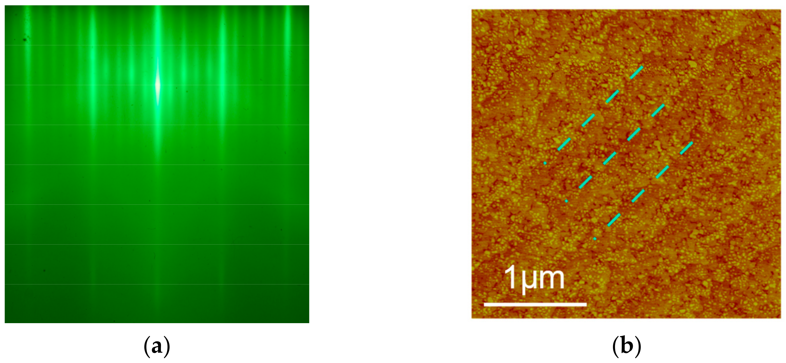
Our first concern is the compatibility of the LSAO layer with the LSCO layer in the MBE growth. We look at this problem from both the surface and interface aspects. Figure 2 displays a typical in-situ RHEED image and an ex-situ AFM image of the superlattice surface. The long main streaks, a bright specular spot, visible Laüe-circle reflections, and Kikuchi lines in the RHEED image in Figure 2a are features characteristic of a very smooth surface without second-phase precipitation. Correspondingly, in the AFM image in Figure 2b, the presence of stepped terrace morphology indicates that the film follows the steps in the substrate due to a small miscut (typically less than 0.5°). The RMS roughness of the sample is only 0.32 nm which is lower than the height of an LSCO monolayer (0.66 nm). The combination of RHEED and AFM images indicates that our superlattice surface is atomically flat.
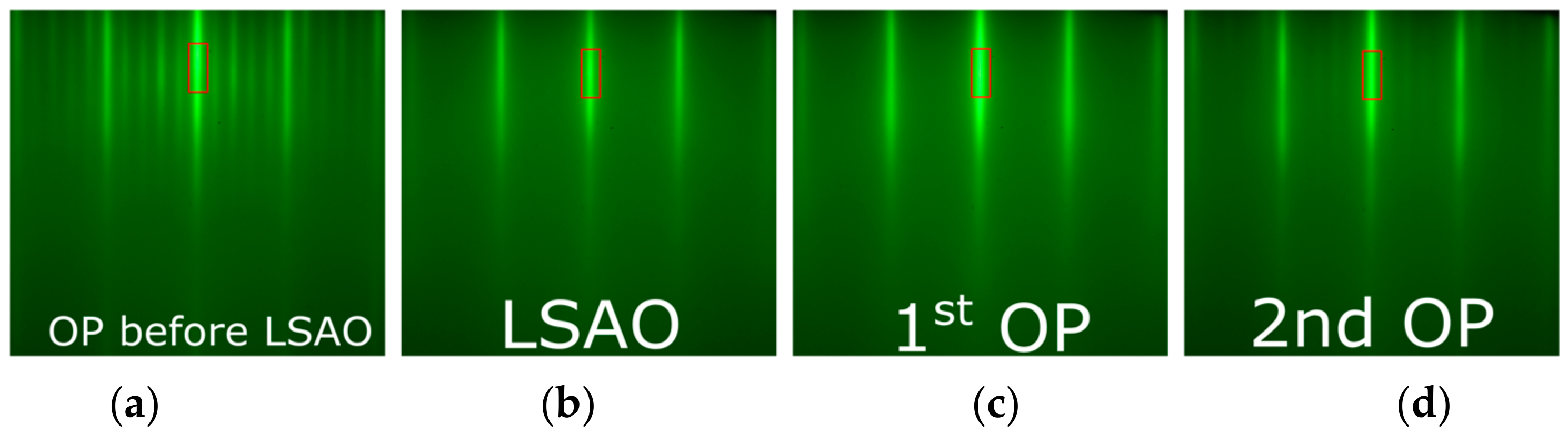
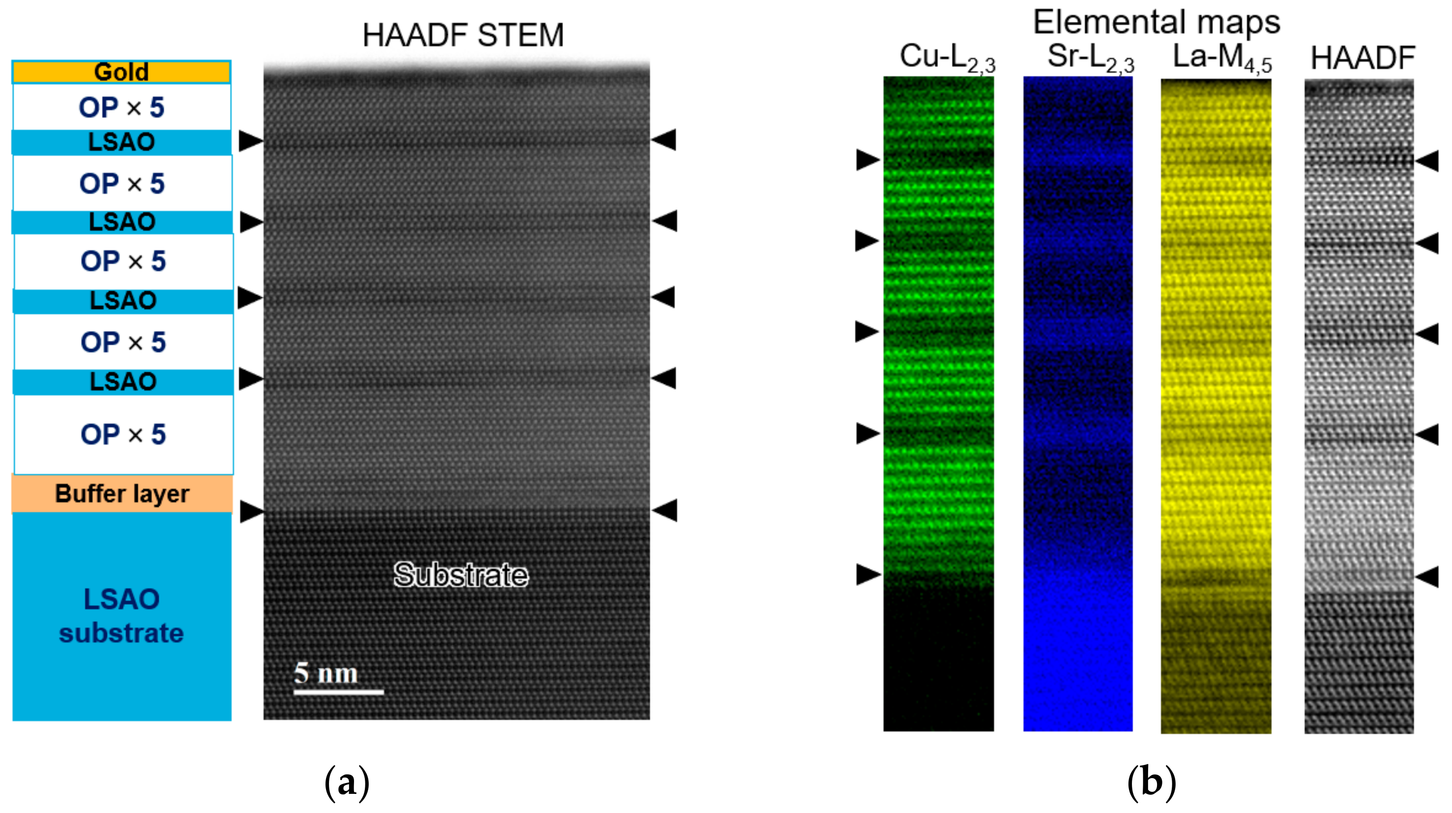
RHEED images of different layers during the growth of one superlattice film, and the corresponding RHEED intensity oscillation plot, are shown in Figure 3. In Figure 3a, the RHEED pattern of the OP layer features a characteristic four-sideband pattern that is identical to that of single-crystal OP films. After the deposition of one monolayer of LSAO, as shown in Figure 3b, the sidebands suddenly disappeared, and the diffraction pattern looked the same as that of an LSAO substrate. Then in Figure 3c,d, the sidebands gradually reappear. Even though the detailed physics behind the sideband reconstruction and its correlation with LSCO superconductivity is still unclear, the fast changes in the RHEED pattern after LSAO and OP layers indicate a sharp interface. Meanwhile, the main streaks remained long and sharp during the growth, indicating that the sample surface remained smooth and free of secondary precipitates as the LSAO and LSCO layers were deposited on top of each other.
The RHEED intensity is another quantitative indicator of surface flatness and interfaces sharpness. In Figure 3e, even though the brightness undergoes a drop during the LSAO layer, it regains intensity in the subsequent OP layer. The overall intensity did not decay over time meaning that the sample surface remained quite flat even after many layers. Note that one oscillation period corresponds to the growth of one monolayer and that the characteristic RHEED oscillation patterns of OP are different from that of LSAO. As shown in Figure 3e, one can observe abrupt changes in the oscillation shapes and amplitudes between LSAO and OP layers, reinforcing the conclusion that the interface is atomically sharp.
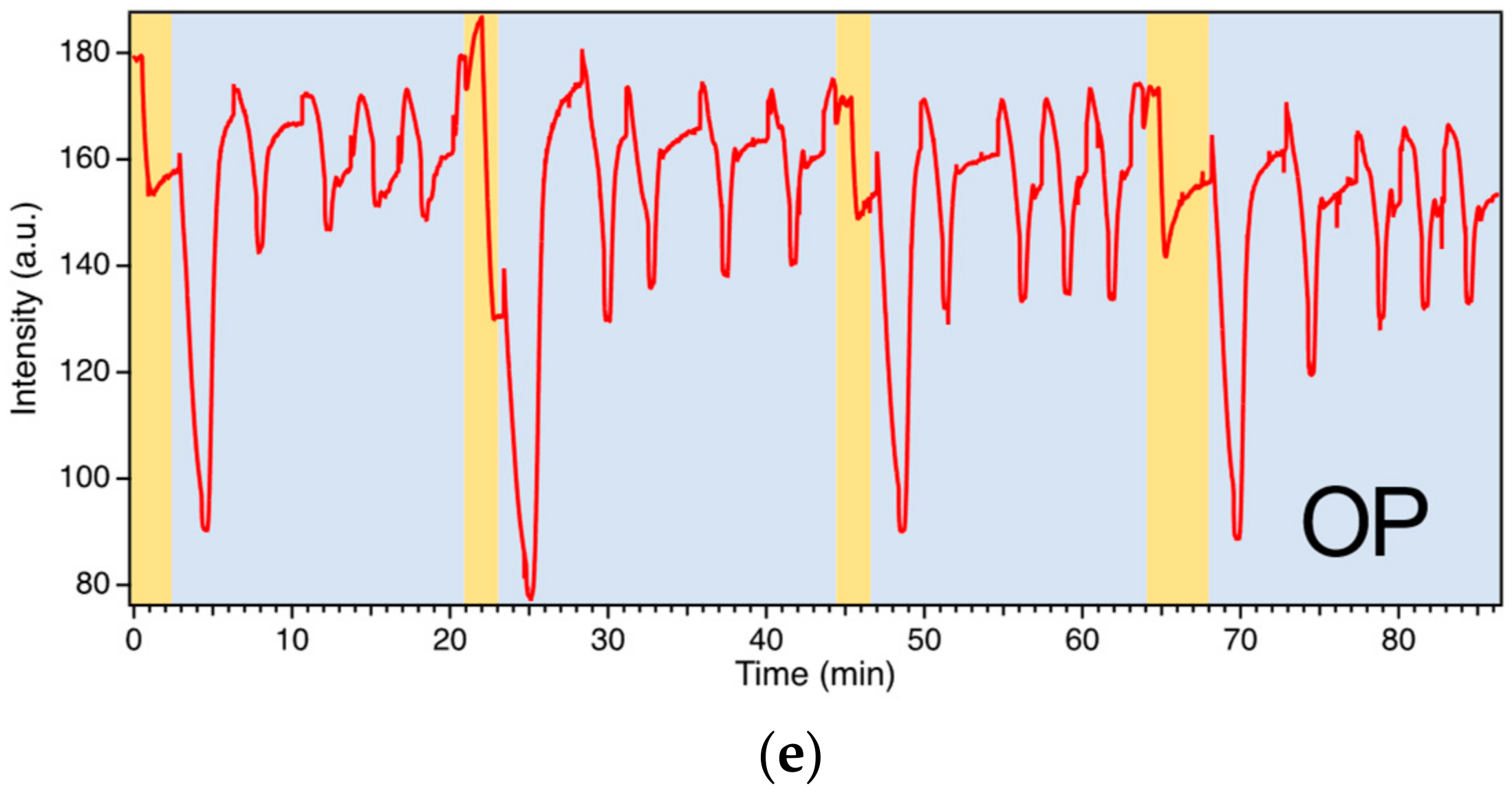
The microstructure of the superlattice (5 × OP):(1 × LSAO) was analyzed by the high-angle annular dark-field (HAADF) STEM (Z-contrast imaging), as shown in Figure 4. Four super-periods can be identified by the apparent difference in image intensity between the LSAO (low-Z) and LSCO (high-Z) layers. Elemental maps correspond well to the superlattice structure. The overall STEM data indicate that superlattices have sharp interfaces.
3.2. Analysis of the Interface Perfection Using Superlattices
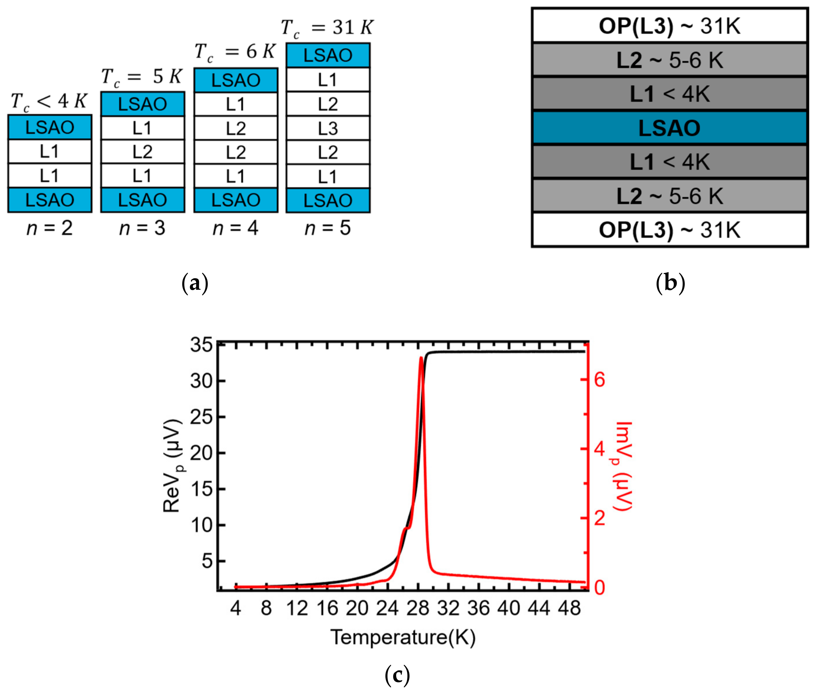
We now consider the “dead” layer issue. The results of the mutual inductance measurement are summarized in Table 1 for four different superlattice films, with OP layer thickness increasing in the steps of one monolayer; the onset of the sharp peak in the imaginary (dissipative) component of the inductance data (Figure 5c) indicates the Tc of the film. Our key result is the evolution of Tc with the number of OP layers. For n < 5, the superlattice samples have low Tc or are not even superconducting down to 4 K. When the OP thickness reaches five monolayers, there is a surge in Tc.
We use a simple approximation model to interpret this result: assuming that OP layers are affected mostly by their nearest LSAO layer, we label OP layers as Layer 1 (L1), Layer 2 (L2), and Layer 3 (L3) according to their distance to the LSAO layer, as illustrated in Figure 5a. Because the abrupt change happens at n = 5, we infer that the Tc of L3 is 31 K. Although the Tc of L3 is not yet as high as 40 K in single crystal LSCO films, it is high enough for L3 to be useful to us as the first “alive” superconducting layer, while L1 and L2 are “dead” layers. The implication of this result for trilayer tunnel junctions is that two “dead” layers, L1 and L2, exist above and below the monolayer LSAO barrier, as shown in Figure 5b. This renders the actual barrier thickness of five monolayers (~3.27 nm). We address the question of the origins of the Tc suppression by analyzing the results of transport experiments and offering more general comments in the Discussion.
Transport measurements were performed on superlattices #1, #2, and #4. The results are summarized in Figure 6 (due to device fabrication issues, we were not able to complete the transport measurement for sample #3). In the literature, various criteria were used to define Tc on an R–T curve, such as the onset of the resistance drop, the point where the slope is maximal, or the point at which the resistance dropped by a certain percentage. Note that Tc inferred from mutual inductance data is at the onset of the Meissner screening. This requires the whole film to become superconducting. So, for consistency, in the R□–T curve, we choose as the sample Tc the temperature at which the resistance drops by >99%. The Tc values of the superlattice films obtained according to this definition from Figure 6a are consistent with those inferred from the mutual inductance measurements. Comparing the R□–T curves of different samples, the Tc of sample #4 is significantly higher, and its R□ in the normal state is about an order of magnitude lower than that of the remaining two samples.
In what follows, we estimate the resistivity of each layer. Here we employ a model of parallel resistors, as illustrated in Figure 6b. We first classify the OP layers as L1, L2, and L3 in the same way as before. Since the transport properties in cuprates are highly anisotropic, the in-plane conductance is a few orders larger than the out-of-plane conductance. Hence, we approximate that the currents only flow in-plane in OP layers, and the current distributes among different super-periods along the c-axis. The superlattice thus can be perceived as a collection of parallel resistors. Because superlattice #1 only contains L1, the value of L1 layer resistivity ρL1 can be directly obtained from the R□ value. Next, using ρL1 and the R□ data of superlattice #2, ρL2 can be derived. Once ρL1 and ρL2 are known, ρL3 can be calculated in a similar way using the R□ data from superlattice #4. All ρ–T curves are plotted in Figure 6c. There is a small bump before the superconducting transition in ρ-T curves of samples #1 and #2; this feature is observed in very underdoped bulk-crystal LSCO samples. On the other hand, the normal-state part of the ρ-T curve of superlattice #4 is linear, as observed in OP or overdoped LSCO crystals. Comparing the resistivities of three different layers with the resistivities of the corresponding LSCO single crystals with the same Tc, their magnitudes are all in a reasonable range. The shape and magnitude of the resistivity curves hint that the primary cause of the formation of “dead” layers L1 and L2 may be carrier depletion. This is consistent with the inferences from earlier studies of trilayer SIS junctions with S = Bi2Sr2CaCu2O8 and I = SrTiO3, BaTiO3, CaTiO3, etc., [36].
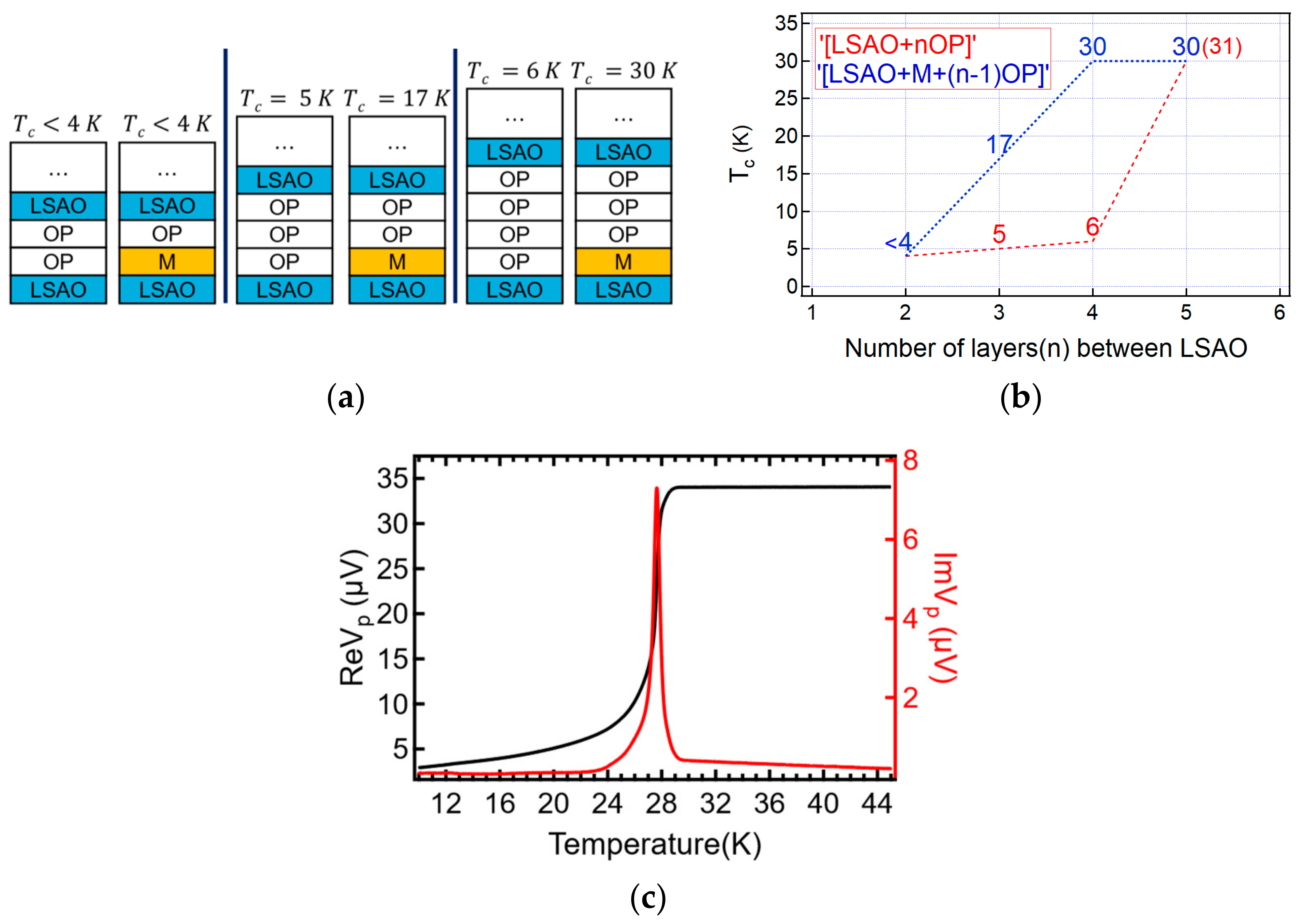
3.3. Introducing an Overdoped Protective Layer
Due to the existence of “dead” layers, the effective barrier is apparently too thick to allow coherent Josephson tunneling. If the underlying cause is that the layers L1 and L2 are depleted of charge carriers (holes), one way of trying to heal the “dead” layer is by increasing the doping level of the LSCO near the interface. With this motivation, we synthesized a new series of superlattice films. The first superconducting layer in the superlattice is replaced with a metallic highly overdoped La1.6Sr0.4CuO4 layer (M). The mutual inductance measurement results of the new superlattices are summarized in Figure 7. Comparing the samples of the same thickness, the new superlattices with an M layer embedded have a significantly higher Tc when n > 2, and the thickness required for a superlattice to reach a high Tc is one or two layers thinner. Thus, once we replace one OP layer with M, one or two OP layers above M are no longer carrier-depleted. Since this new superlattice structure is not symmetrical, it cannot be simply modeled and understood using L1, L2, and L3 as before. We are conducting further tests and theoretical studies to reveal the difference the M layer makes. What seems clear already at this point, though, is that carrier depletion is indeed the main mechanism of “dead” layer formation.
4. Discussion
The experimental observations presented here raise questions about the microscopic origin of the creation of “dead” layers and Tc reduction in ultrathin LSCO films proximal to LSAO. This was understood to be a general problem with cuprate interfaces with other oxides; the interfacial layers undergo dramatic atomic and electronic reconstruction modifying their physical properties [19,37,38,39,40,41,42,43,44]. For this reason, the fabrication of HTS SIS Josephson junctions remained elusive despite great motivation, massive efforts by many groups worldwide, and billions of dollars invested [3]. However, the study of the physical properties of buried interfaces has been notoriously difficult and a detailed microscopic understanding of interface reconstruction is still lacking.
In very general terms, the reason for the reconstruction and Tc reduction ought to be in the “mismatch” between the film and the substrate. This can be broken into several aspects [37,38,39,40,41,42,43,44].
- (i)
- The geometric mismatch: the in-plane lattice constants of LSCO are larger compared to LSAO. The LSCO layers are under compressive Poisson strain, which creates misfit dislocations, domains, etc. However, this is likely not the main problem—we can grow LSCO films on LSAO substrates with Tc ≳ 40 K.
- (ii)
- The chemical mismatch: one compound contains Cu and the other Al. The entropy is driving Cu-Al intermixing. To prevent this, we need to find the “ALL-MBE window” in the (T, p) space where the bulk ion mobility is low (so that there is no cation interdiffusion) while the surface mobility is high (so that the film forms the desired crystal structure). Controlled post-annealing can help improve crystallinity. Our STEM data (Figure 4) show that we succeeded to a large extent. However, we cannot rule out having some Al atoms on Cu sites. Replacing Cu2+ with Al3+ adds one electron and removes one hole from the CuO2 plane. In addition, such charged defects act as strong unitary scatterers and pair breakers, reducing the superfluid density and Tc.
- (iii)
- The electrostatic mismatch: the sequence of effective charges of atomic layers in LCO is (LaO)+1–(CuO2)−2–(LaO)+1, different from that in LSAO, viz., (La0.5SrO)+0.5–(AlO2)−1–(La0.5SrO)+0.5. This leads to the so-called “polarization catastrophe” and the “Madelung strain” [45]. To maintain charge neutrality, the growing film adjusts its composition by changing the sticking rates, so the cation ratios (e.g., La vs. Cu) may vary. STEM studies [46,47] showed that the first couple of MLs of LSCO on LSAO are heavily reconstructed—in fact, the actual structure of the “interface compound” is unrelated to the regular “214” (or “K2NiF4”) structure of bulk LSCO. For the same reasons, oxygen vacancies may abound in the LSCO layer(s) next to the interface. Another consequence is dramatic ionic displacements and structural modifications in the layers next to the interface or to the free surface [48].
- (iv)
- The electronic mismatch: the electrochemical potentials in the two materials are different. This can cause electron transfer (depletion and accumulation) across the interface, modifying the electronic properties in both the nearby superconducting and insulating layers.
While the above may all be present, we believe that the main effect is probably hole depletion, largely due to oxygen vacancies. We hope to shed new light on this important question by future experimentation, including STEM and high-resolution electron-energy loss spectroscopy (HR-EELS) to reveal the carrier density distribution and oxygen profile along the c-axis.
5. Conclusions
We demonstrated the capability of synthesizing LSCO-LSAO-LSCO heterostructures with atomically flat surfaces and sharp interfaces using a state-of-the-art ALL-MBE system. Using multiple characterization tools and the superlattice test method, we probe the perfection of the interface and identify the “dead” layer thickness in such junctions. Our mutual inductance tests on LSCO-LSAO superlattices indicate an effective barrier thickness of five monolayers due to the presence of “dead” layers. Transport measurements imply that the presence of “dead” layers may be due to carrier depletion. Consistent with this, we found that the thickness of the “dead” layer can be reduced if the hole depletion in LSCO layer next to LSAO is compensated by increasing the chemical doping level.
At this point, we are still working on achieving our ultimate goal, i.e., the fabrication of high-quality LSCO S-I-S Josephson junctions, but our current research has shed light on future directions. For superlattices that contain LSAO layers, additional characterization techniques, possibly including STEM and HR-EELS, are needed to fully understand the underlying mechanism of the formation of “dead” LSCO layers. The superlattice structure and growth recipe can be fine-tuned further to explore the influence of other parameters, for example, the LSCO doping level, post-annealing time, and pressure. On the other hand, we can also test different complex oxides as candidate barrier materials by means of the superlattice test method presented here.
Author Contributions
I.B. and X.H. conceived the superlattice synthesis schemes. X.H. and X.X. synthesized films and performed AFM and mutual inductance measurements. A.T.B. performed the microfabrication processing. A.T.B., X.H. and X.X. performed R–T measurements. M.-G.H. performed STEM measurements. I.B., Y.Z. and X.S. supervised the project. X.X. drafted the manuscript. All authors have read and agreed to the published version of the manuscript.
Funding
This research was supported by the DOE, Basic Energy Sciences, Materials Science and Engineering Division, under Contract No. DE-SC0012704. X. H. is supported by the Gordon and Betty Moore Foundation’s EPiQS Initiative through grant GBMF9074.
Data Availability Statement
All data are available upon reasonable request.
Conflicts of Interest
The authors declare no conflict of interest.
References
- Kirtley, J.R.; Tafuri, F. Tunneling Measurements of the Cuprate Superconductors. In Handbook of High-Temperature Superconductivity; Springer New York: New York, NY, USA, 2007; pp. 19–86. [Google Scholar] [CrossRef]
- Fundamentals and Frontiers of the Josephson Effect; Tafuri, F. (Ed.) Springer Series in Materials Science; Springer International Publishing: Cham, Switzerland, 2019; Volume 286, ISBN 978-3-030-20724-3. [Google Scholar] [CrossRef]
- Tafuri, F.; Massarotti, D.; Galletti, L.; Stornaiuolo, D.; Montemurro, D.; Longobardi, L.; Lucignano, P.; Rotoli, G.; Pepe, G.P.; Tagliacozzo, A.; et al. Recent Achievements on the Physics of High-T C Superconductor Josephson Junctions: Background, Perspectives and Inspiration. J. Supercond. Nov. Magn. 2012, 26, 21–41. [Google Scholar] [CrossRef]
- Hilgenkamp, H.; Mannhart, J. Grain boundaries in high-Tcsuperconductors. Rev. Mod. Phys. 2002, 74, 485–549. [Google Scholar] [CrossRef]
- Mannhart, J.; Chaudhari, P.; Dimos, D.; Tsuei, C.C.; McGuire, T.R. Critical Currents in [001] Grains and across Their Tilt Boundaries in YBa2Cu3O7 Films. Phys. Rev. Lett. 1988, 61, 2476–2479. [Google Scholar] [CrossRef] [PubMed]
- Herrmann, K.; Kunkel, G.; Siegel, M.; Schubert, J.; Zander, W.; Braginski, A.I.; Jia, C.L.; Kabius, B.; Urban, K. Correlation of YBa2Cu3O7step-edge junction characteristics with microstructure. J. Appl. Phys. 1995, 78, 1131–1139. [Google Scholar] [CrossRef]
- Poppe, U.; Divin, Y.; Faley, M.; Wu, J.; Jia, C.; Shadrin, P.; Urban, K. Properties of YBa/sub 2/Cu/sub 3/O/sub 7/ thin films deposited on substrates and bicrystals with vicinal offcut and realization of high I/sub c/R/sub n/ junctions. IEEE Trans. Appl. Supercond. 2001, 11, 3768–3771. [Google Scholar] [CrossRef]
- Bauch, T.; Lindström, T.; Tafuri, F.; Rotoli, G.; Delsing, P.; Claeson, T.; Lombardi, F. Quantum Dynamics of a d-Wave Josephson Junction. Science 2006, 311, 57–60. [Google Scholar] [CrossRef]
- Smilde, H.J.H.; Ariando, A.; Blank, D.H.A.; Gerritsma, G.J.; Hilgenkamp, H.; Rogalla, H. d-Wave–Induced Josephson Current Counterflow inYBa2Cu3O7/NbZigzag Junctions. Phys. Rev. Lett. 2002, 88, 057004. [Google Scholar] [CrossRef]
- Char, K.; Colclough, M.S.; Garrison, S.M.; Newman, N.; Zaharchuk, G. Bi-epitaxial grain boundary junctions in YBa2Cu3O7. Appl. Phys. Lett. 1991, 59, 733–735. [Google Scholar] [CrossRef]
- Antognazza, L.; Moeckly, B.H.; Geballe, T.H.; Char, K. Properties of high-TcJosephson junctions withY0.7Ca0.3Ba2Cu3O7−δbarrier layers. Phys. Rev. B 1995, 52, 4559–4567. [Google Scholar] [CrossRef]
- Katz, A.S.; Sun, A.G.; Dynes, R.C.; Char, K. Fabrication of all thin-film YBa2Cu3O7−δ /Pb Josephson tunnel junctions. Appl. Phys. Lett. 1995, 66, 105–107. [Google Scholar] [CrossRef]
- Il’Ichev, E.; Grajcar, M.; Hlubina, R.; Ijsselsteijn, R.P.J.; Hoenig, H.E.; Meyer, H.-G.; Golubov, A.; Amin, M.H.S.; Zagoskin, A.M.; Omelyanchouk, A.N.; et al. Degenerate Ground State in a MesoscopicYBa2Cu3O7−xGrain Boundary Josephson Junction. Phys. Rev. Lett. 2001, 86, 5369–5372. [Google Scholar] [CrossRef]
- Lombardi, F.; Tafuri, F.; Ricci, F.; Granozio, F.M.; Barone, A.; Testa, G.; Sarnelli, E.; Kirtley, J.R.; Tsuei, C.C. Intrinsic d-Wave Effects in YBa2Cu3O7−δ Grain Boundary Josephson Junctions. Phys. Rev. Lett. 2002, 89, 207001. [Google Scholar] [CrossRef]
- Bauch, T.; Lombardi, F.; Tafuri, F.; Barone, A.; Rotoli, G.; Delsing, P.; Claeson, T. Macroscopic Quantum Tunneling in d-Wave YBa2Cu3O7−δ Josephson Junctions. Phys. Rev. Lett. 2005, 94, 087003. [Google Scholar] [CrossRef]
- Tafuri, F.; Kirtley, J.R. Weak links in high critical temperature superconductors. Rep. Prog. Phys. 2005, 68, 2573–2663. [Google Scholar] [CrossRef]
- Lucignano, P.; Stornaiuolo, D.; Tafuri, F.; Altshuler, B.L.; Tagliacozzo, A. Evidence for a Minigap in YBCO Grain Boundary Josephson Junctions. Phys. Rev. Lett. 2010, 105, 147001. [Google Scholar] [CrossRef]
- Longobardi, L.; Massarotti, D.; Stornaiuolo, D.; Galletti, L.; Rotoli, G.; Lombardi, F.; Tafuri, F. Direct Transition from Quantum Escape to a Phase Diffusion Regime in YBaCuO Biepitaxial Josephson Junctions. Phys. Rev. Lett. 2012, 109, 050601. [Google Scholar] [CrossRef]
- Naito, M.; Yamamoto, H.; Sato, H. Intrinsic problem of cuprate surface and interface: Why good tunnel junctions are difficult to fabricate. Phys. C Supercond. Appl. 2000, 335, 201–206. [Google Scholar] [CrossRef]
- Bozovic, I.; Eckstein, J. Atomic-level engineering of cuprates and manganites. Appl. Surf. Sci. 1997, 113–114, 189–197. [Google Scholar] [CrossRef]
- Bozovic, I.; Eckstein, J.N.; Virshup, G.F.; Chaiken, A.; Wall, M.; Howell, R.; Fluss, M. Atomic-layer engineering of cuprate superconductors. J. Supercond. 1994, 7, 187–195. [Google Scholar] [CrossRef]
- Bozovic, I. Atomic-layer engineering of superconducting oxides: Yesterday, today, tomorrow. IEEE Trans. Appl. Supercond. 2001, 11, 2686–2695. [Google Scholar] [CrossRef]
- Xu, X.; He, X.; Shi, X.; Božović, I. Synthesis of La2−xSrxCuO4 films via atomic layer-by-layer molecular beam epitaxy. APL Mater. 2022, 10, 061103. [Google Scholar] [CrossRef]
- Bozovic, I.; Logvenov, G.; Verhoeven, M.A.J.; Caputo, P.; Goldobin, E.; Geballe, T.H. No mixing of superconductivity and antiferromagnetism in a high-temperature superconductor. Nature 2003, 422, 873–875. [Google Scholar] [CrossRef]
- Bozovic, I.; Logvenov, G.; Verhoeven, M.A.J.; Caputo, P.; Goldobin, E.; Beasley, M.R. Giant Proximity Effect in Cuprate Superconductors. Phys. Rev. Lett. 2004, 93, 157002. [Google Scholar] [CrossRef]
- Sato, H.; Naito, M. Increase in the superconducting transition temperature by anisotropic strain effect in (001) La1.85Sr0.15CuO4 thin films on LaSrAlO4 substrates. Phys. C Supercond. Appl. 1997, 274, 221–226. [Google Scholar] [CrossRef]
- Sato, H.; Tsukada, A.; Naito, M.; Matsuda, A. La-214 thin films under epitaxial strain. Phys. C Supercond. Appl. 2000, 341–348, 1767–1770. [Google Scholar] [CrossRef]
- Sato, H.; Tsukada, A.; Naito, M. La-214 thin films under epitaxial strain. Phys. C Supercond. Appl. 2004, 408–410, 848–852. [Google Scholar] [CrossRef]
- Cieplak, M.Z.; Berkowski, M.; Abal’Oshev, A.; Guha, S.; Wu, Q. The effect of strain on the microstructure and superconductivity of pulsed laser deposited LaSrCuO films. Supercond. Sci. Technol. 2006, 19, 564–572. [Google Scholar] [CrossRef]
- Li, B.-S.; Sawa, A.; Okamoto, H. Suppression of Precipitates in the La2-xSrxCuO4 Films Grown on LaSrAlO4 Substrates by Introducing Homoepitaxial Layer. Jpn. J. Appl. Phys. 2011, 50, 093101. [Google Scholar] [CrossRef]
- Lagally, M.; Savage, D. Quantitative Electron Diffraction from Thin Films. MRS Bull. 1993, 18, 24–31. [Google Scholar] [CrossRef]
- Daweritz, L.; Ploog, K. Contribution of reflection high-energy electron diffraction to nanometre tailoring of surfaces and interfaces by molecular beam epitaxy. Semicond. Sci. Technol. 1994, 9, 123–136. [Google Scholar] [CrossRef]
- Kawamura, T.; Maksym, P. RHEED wave function and its applications. Surf. Sci. Rep. 2009, 64, 122–137. [Google Scholar] [CrossRef]
- Hafez, M.A.; Zayed, M.K.; Elsayed-Ali, H.E. Review: Geometric Interpretation of Reflection and Transmission RHEED Patterns. Micron 2022, 159, 103286. [Google Scholar] [CrossRef]
- He, X.; Gozar, A.; Sundling, R.; Božović, I. High-precision measurement of magnetic penetration depth in superconducting films. Rev. Sci. Instruments 2016, 87, 113903. [Google Scholar] [CrossRef]
- Bozovic, I.; Eckstein, J.N. Superconductivity in Cuprate Superlattices. In Physical Properties of High Temperature Superconductors V; World Scientific: Singapore, 1996; pp. 99–207. [Google Scholar] [CrossRef]
- Noguera, C. Polar oxide surfaces. J. Phys. Condens. Matter 2000, 12, R367–R410. [Google Scholar] [CrossRef]
- Nakagawa, N.; Hwang, H.Y.; Muller, D. Why some interfaces cannot be sharp. Nat. Mater. 2006, 5, 204–209. [Google Scholar] [CrossRef]
- Chakhalian, J.; Freeland, J.W.; Habermeier, H.-U.; Cristiani, G.; Khaliullin, G.; van Veenendaal, M.; Keimer, B. Orbital Reconstruction and Covalent Bonding at an Oxide Interface. Science 2007, 318, 1114–1117. [Google Scholar] [CrossRef]
- Mannhart, J.; Blank, D.; Hwang, H.; Millis, A.; Triscone, J.-M. Two-Dimensional Electron Gases at Oxide Interfaces. MRS Bull. 2008, 33, 1027–1034. [Google Scholar] [CrossRef] [Green Version]
- Chen, H.; Kolpak, A.M.; Ismail-Beigi, S. Fundamental asymmetry in interfacial electronic reconstruction between insulating oxides: An Ab Initio Study. Phys. Rev. B 2009, 79, 161402. [Google Scholar] [CrossRef]
- Cantoni, C.; Gazquez, J.; Granozio, F.M.; Oxley, M.P.; Varela, M.; Lupini, A.R.; Pennycook, S.J.; Aruta, C.; Di Uccio, U.S.; Perna, P.; et al. Electron Transfer and Ionic Displacements at the Origin of the 2D Electron Gas at the LAO/STO Interface: Direct Measurements with Atomic-Column Spatial Resolution. Adv. Mater. 2012, 24, 3952–3957. [Google Scholar] [CrossRef]
- Huang, Z.; Ariando; Wang, X.R.; Rusydi, A.; Chen, J.; Yang, H.; Venkatesan, T. Interface Engineering and Emergent Phenomena in Oxide Heterostructures. Adv. Mater. 2018, 30, e1802439. [Google Scholar] [CrossRef]
- Kouser, S.; Pantelides, S.T. Quantum physical reality of polar-nonpolar oxide heterostructures. Phys. Rev. B 2021, 104, 075411. [Google Scholar] [CrossRef]
- Butko, V.Y.; Logvenov, G.; Božović, N.; Radović, Z.; Božović, I. Madelung Strain in Cuprate Superconductors—A Route to Enhancement of the Critical Temperature. Adv. Mater. 2009, 21, 3644–3648. [Google Scholar] [CrossRef]
- Locquet, J.-P.; Perret, J.; Fompeyrine, J.; Mächler, E.; Seo, J.W.; van Tendeloo, G. Doubling the Critical Temperature of LSCO Using Epitaxial Strian. Nature 1998, 394, 453–456. [Google Scholar] [CrossRef]
- He, J.; Klie, R.F.; Logvenov, G.; Bozovic, I.; Zhu, Y. Microstructure and possible strain relaxation mechanisms of La2CuO4+δ thin films grown on LaSrAlO4 and SrTiO3 substrates. J. Appl. Phys. 2007, 101, 073906. [Google Scholar] [CrossRef]
- Zhou, H.; Yacoby, Y.; Butko, V.Y.; Logvenov, G.; Božović, I.; Pindak, R. Anomalous expansion of the copper-apical-oxygen distance in superconducting cuprate bilayers. Proc. Natl. Acad. Sci. USA 2010, 107, 8103–8107. [Google Scholar] [CrossRef] [Green Version]
Figure 1.
The design of LSCO-LSAO superlattice samples. The buffer layer is typically a one-unit cell thick layer of highly overdoped LSCO (x = 0.40). It helps form the proper “214” crystal structure and suppresses the nucleation of precipitates of unwanted secondary phases at the substrate/film interface.

Figure 2.
Characterization of the surface of superlattice film: (a) RHEED image of the final layer. Five main streaks originate from the (0, −2), (0, −1), (0, 0), (0, 1), and (0, 2) Bragg diffraction rods; (b) An AFM image of an (LSCO (x = 0.40) + 2 × OP):(1 × LSAO) superlattice sample. The total film thickness is 12.42 nm. The field of view is 3 × 3 μm2. Terrace steps are marked with blue lines. The RMS roughness is 0.32 nm. We specifically grew this sample without in situ gold coating so that we could obtain an AFM image of the films surface. This surface morphology is representative of our LSCO films and superlattices.

Figure 3.
RHEED analysis during the growth of a (5 × OP):(1 × LSAO) superlattice film: (a) The RHEED image of an OP layer before the growth of LSAO; (b) the RHEED image when the LSAO layer is completed; (c) the RHEED image after the first OP layer is grown on top of LSAO in (b); (d) The RHEED image of the second OP layer grown on top of the first OP layer; (e) the RHEED intensity oscillations detected by measuring the brightness within red rectangles in panels (a–d), encompassing the specular spot. Yellow: deposition of LSAO layer. Purple: deposition of OP layers. The plot shows the growth process of four superlattice periods (note that the growth time of each monolayer is not directly representative because we manually adjusted the annealing time or shuttering time according to the RHEED feedback to maintain a correct stoichiometry and improve the film quality.).


Figure 4.
STEM characterization of a superlattice sample: (a) HAADF-STEM image of the superlattice structure; (b) Cu, Sr, and La elemental mapping along the [001] direction of the same sample.
Figure 4.
STEM characterization of a superlattice sample: (a) HAADF-STEM image of the superlattice structure; (b) Cu, Sr, and La elemental mapping along the [001] direction of the same sample.

Figure 5.
Interpretation of the mutual inductance data: (a) The OP layers inside the superlattice samples are categorized according to the model as L1, L2, and L3; (b) the schematics of the junction interface in the presence of dead layers. The actual barrier thickness is estimated by adding the thickness of one LSAO monolayer (0.63 nm) and four LSCO monolayers (4 × 0.66 nm = 2.64 nm); (c) the mutual inductance data for a (5 × OP):(1 × LSAO) superlattice. Left ordinate: the real (in-phase) component of Vp. Right ordinate: The imaginary part of Vp. As read from the onset of the sharp rise in ImVp, Sample Tc = 31 K.

Figure 6.
In-plane electrical transport measurement data of LSCO-LSAO superlattices. (a) The R□ (T) dependence in different superlattices, where R□ is the resistance per square. The point where the resistance value drops by >99% is marked with a red arrow. For superlattice #1, Tc is below4 K, the lowest-T limit of this measurement setup; (b) the model of parallel resistors. (c) the dependence of resistivity on the temperature of different OP layers derived from the R□–T curves.

Figure 7.
Measurement results of superlattices embedded with one M layer. (a) Schematic of superlattice structures. The Tc of each sample is indicated above each image to facilitate the comparison of superlattices with and without the M layer; (b) evolution of Tc with the number of LSCO layers between two LSAO layers. Red: superlattices without the M layer. Blue: superlattices with one M layer embedded; (c) Mutual inductance data for (M + 3 × OP):(1 × LSAO) superlattice. From the onset of the sharp rise in ImVp, we infer Tc = 30 K.


Table 1.
Superconducting transition temperature measured by mutual inductance for four (n × OP):(1 × LSAO) superlattices.
Table 1.
Superconducting transition temperature measured by mutual inductance for four (n × OP):(1 × LSAO) superlattices.
| Sample # | Unit Cell Structure | Number of OP Layers | Tc |
|---|---|---|---|
| 1 | (2 × OP):(1 × LSAO) | 2 | <4 K 1,2 |
| 2 | (3 × OP):(1 × LSAO) | 3 | 5 K |
| 3 | (4 × OP):(1 × LSAO) | 4 | 6 K |
| 4 | (5 × OP):(1 × LSAO) | 5 | 31 K |
1 The lowest temperature limit of our mutual inductance system is 4 K. 2 Since the sample with n = 2 has Tc < 4 K, there was no point in synthesizing and studying a sample with n = 1.
Disclaimer/Publisher’s Note: The statements, opinions and data contained in all publications are solely those of the individual author(s) and contributor(s) and not of MDPI and/or the editor(s). MDPI and/or the editor(s) disclaim responsibility for any injury to people or property resulting from any ideas, methods, instructions or products referred to in the content. |
© 2023 by the authors. Licensee MDPI, Basel, Switzerland. This article is an open access article distributed under the terms and conditions of the Creative Commons Attribution (CC BY) license (https://creativecommons.org/licenses/by/4.0/).
Share and Cite
MDPI and ACS Style
Xu, X.; He, X.; Bollinger, A.T.; Han, M.-G.; Zhu, Y.; Shi, X.; Božović, I. A Method to Probe the Interfaces in La2−xSrxCuO4-LaSrAlO4-La2−xSrxCuO4 Trilayer Junctions. Condens. Matter 2023, 8, 21. https://doi.org/10.3390/condmat8010021
AMA Style
Xu X, He X, Bollinger AT, Han M-G, Zhu Y, Shi X, Božović I. A Method to Probe the Interfaces in La2−xSrxCuO4-LaSrAlO4-La2−xSrxCuO4 Trilayer Junctions. Condensed Matter. 2023; 8(1):21. https://doi.org/10.3390/condmat8010021
Chicago/Turabian StyleXu, Xiaotao, Xi He, Anthony T. Bollinger, Myung-Geun Han, Yimei Zhu, Xiaoyan Shi, and Ivan Božović. 2023. "A Method to Probe the Interfaces in La2−xSrxCuO4-LaSrAlO4-La2−xSrxCuO4 Trilayer Junctions" Condensed Matter 8, no. 1: 21. https://doi.org/10.3390/condmat8010021