
New Scaling Laws for Pinning Force Density in Superconductors

M.N. Miheev Institute of Metal Physics, Ural Branch, Russian Academy of Sciences, 18, S. Kovalevskoy St, 620108 Ekaterinburg, Russia
Condens. Matter 2022, 7(4), 74; https://doi.org/10.3390/condmat7040074
Submission received: 26 October 2022
/
Revised: 4 December 2022
/
Accepted: 8 December 2022
/
Published: 13 December 2022
(This article belongs to the Section Superconductivity)
Abstract
:Since the report by Fietz and Webb (Phys. Rev. 1968, 178, 657–667), who considered the pinning force density, (where Jc is the critical current density and B is applied magnetic flux density), in isotropic superconductors as a unique function of reduced magnetic field, (where is the upper critical field), has been scaled based on the ratio, for which there is a widely used Kramer–Dew–Hughes scaling law of , where , , p, and q are free-fitting parameters. To describe in high-temperature superconductors, the Kramer–Dew–Hughes scaling law has been modified by (a) an assumption of the angular dependence of all parameters and (b) by the replacement of the upper critical field, Bc2, by the irreversibility field, Birr. Here, we note that is also a function of critical current density, and thus, the scaling law should exist. In an attempt to reveal this law, we considered the full function and reported that there are three distinctive characteristic ranges of (where is the self-field critical current density) on which can be splatted. Several new scaling laws for were proposed and applied to MgB2, NdFeAs(O,F), REBCO, (La,Y)H10, and YH6. The proposed scaling laws describe the in-field performance of superconductors at low and moderate magnetic fields, and thus, the primary niche for these laws is superconducting wires and tapes for cables, fault current limiters, and transformers.
1. Introduction
In 1962, Philip W. Anderson wrote [1], “A major difficulty in understanding hard superconductors has been the appreciable temperature dependence of critical currents and fields at temperatures as low as . None of the properties of the bulk superconducting state vary noticeably at this temperature…
…We shall show that this… can be explained by assuming that the mechanism of flux creep is thermally activated motion of bundles of flux lines, aided by the Lorentz force , over free energy barriers coming from the pinning effect of inhomogeneities, strains, dislocations, or other physical defects”.
Since then, the primary idea that the origin of the electric power dissipation in type-II superconductors is Abrikosov’s vortices dissipative movement under the Lorentz force [2] has been unconditionally accepted. Based on this concept, superconducting materials can be characterized by principal quantity, the pinning force density, , defined as:
where Jc(B,T) is the experimentally measured critical current density and B is the applied magnetic flux density.
There is a need to clarify that because is a mechanical force density (which is directly related to the Lorenz force density) applied to the superconducting sample, it is not impossible to build a machine, which will directly measure this mechanical force density with simultaneous measurements of:
- The electric field, E, along the sample;
- The applied magnetic field, Bappl;
- The sample temperature, T;
- The transport current density, J.
Direct measurements in this machine will utilize (E, Bappl, T, J) as independent experimental parameters. Despite the fact that the utilizing now methods of determination are based on the multiplication of the critical current density, Jc(Bappl), and the applied magnetic field, Bappl, it does not alter the fundamental nature of (see, for instance, [1]) and a principal possibility to measure directly. Thus, a conventional way of thinking that is another representation of the measured in the experiment Jc(Bappl) and Bappl can be reconsidered to be more broad.
Fietz and Webb [3] were the first to propose a scaling law for pinning force density:
where K is a numerical multiplicative prefactor, is a function where the independent variable is the Ginzburg–Landau parameter , is the upper critical field, and is a function of a reduced applied magnetic field. Several years later, Kramer [4] and Dew-Hughes [5] developed the most widely used expression for :
where , , p, and q are free-fitting parameters. It should mention that Equation (3) is in use in its normalized form of [6]:
For Nb3Sn-based alloys, Equation (3) was upgraded [7,8,9,10,11] to account for the temperature and the strain dependence of by the introduction of several multiplicative terms in Equation (3):
where C, a, μ, η, , s, and Tc are free-fitting parameters and is given by a different function. On the one hand, Equation (5) is applicable only for Nb3Sn and only at a moderate strain level [7,8,9,10,11]. On the other hand, the upgraded Equation (5) is a fitting function constructed in terms of the general flavor of the two-fluid model, where each new parameter is added to the equation through a multiplicative term of:
where is the fitted value with a new variable; P, , , m, and n are free-fitting parameters; and is a maximal value for the new parameter (it is chosen within a given model; for instance, temperature dependences of the superconducting parameters are generally utilized , which is the maximum temperature at which the superconducting state does exist).
In this regard, there is another often chosen form for the new fitting term based on an exponential function [12], from which we can mention the scaling law proposed by Fietz et al. [13] for Nb-Zr superconductors:
where , , and are free-fitting parameters of the model. The temperature-dependent fitting term also can be represented by an exponential function, as it was proposed for the second-generation high-temperature superconducting wires (2G-wires) by Senatore et al. [14]:
where , and are free-fitting parameters ( [14]).
It should be noted that Equation (8) is internally incorrect because the units of the right hand of the equation are not A/m2 (which are the current density units). This mistake is becoming widely spread because, recently, Francis et al. [15] utilized Equation (8) (which is Equation (1) in [15]) for the analysis of nanostructured coated conductors too.
Overall, for MgB2, cuprates, and iron-based superconductors (IBS), different expressions for were proposed [6,12,13,14,15,16,17,18,19,20,21] (extended review for REBCO given by Jirsa et al. [6]). For these compounds, due to their anisotropic nature, all free-fitting parameters of Equations (3) and (4) are angularly dependent. Additionally, due to the relatively wide transition width in these compounds, the primary ratio in scaling laws (Equations (3) and (4)) is often replaced by , where is the irreversibility field.
Despite some differences, a primary assumption of all known scaling laws [3,4,5,6,7,8,9,10,11,12,13,14,15,16,17,18,19,20,21] is that should have the applied magnetic field, , as a primary variable (Equations (1)–(5)). Thus, all known scaling laws have been developed for values.
In this paper, we pointed out that (Equation (1)) is also a function of . This fact was, somehow, never considered. Thus, the scaling law should also exist. Based on this primary idea, we consider the full function and propose potential scaling laws for in thin film superconductors, which reflect different pinning characteristics of the materials. We limited our paper to the case when an external magnetic field, , is applied, in the perpendicular direction, to the film’s large surface, that is, for the field angle [22].
2. Problem Description
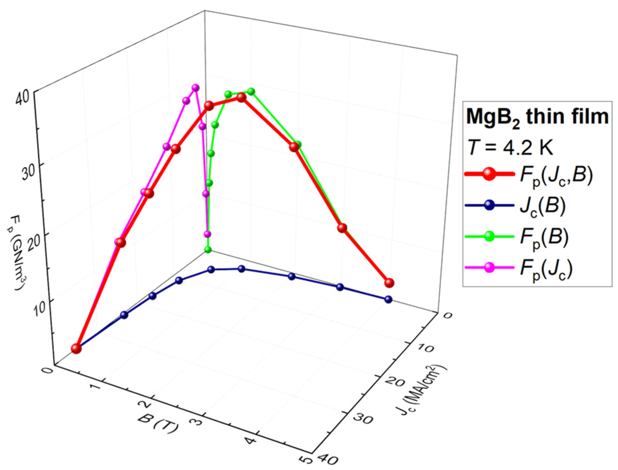
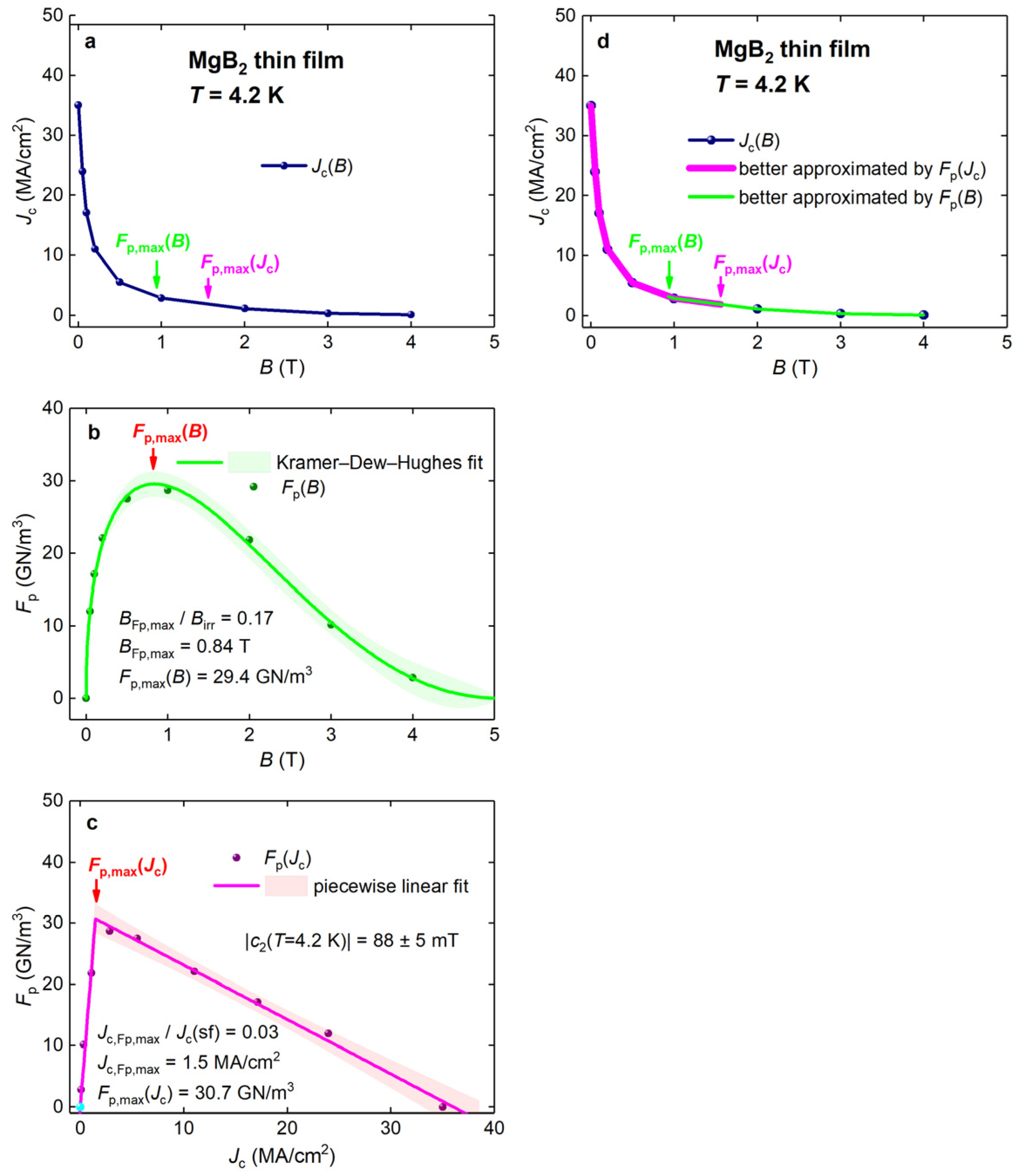
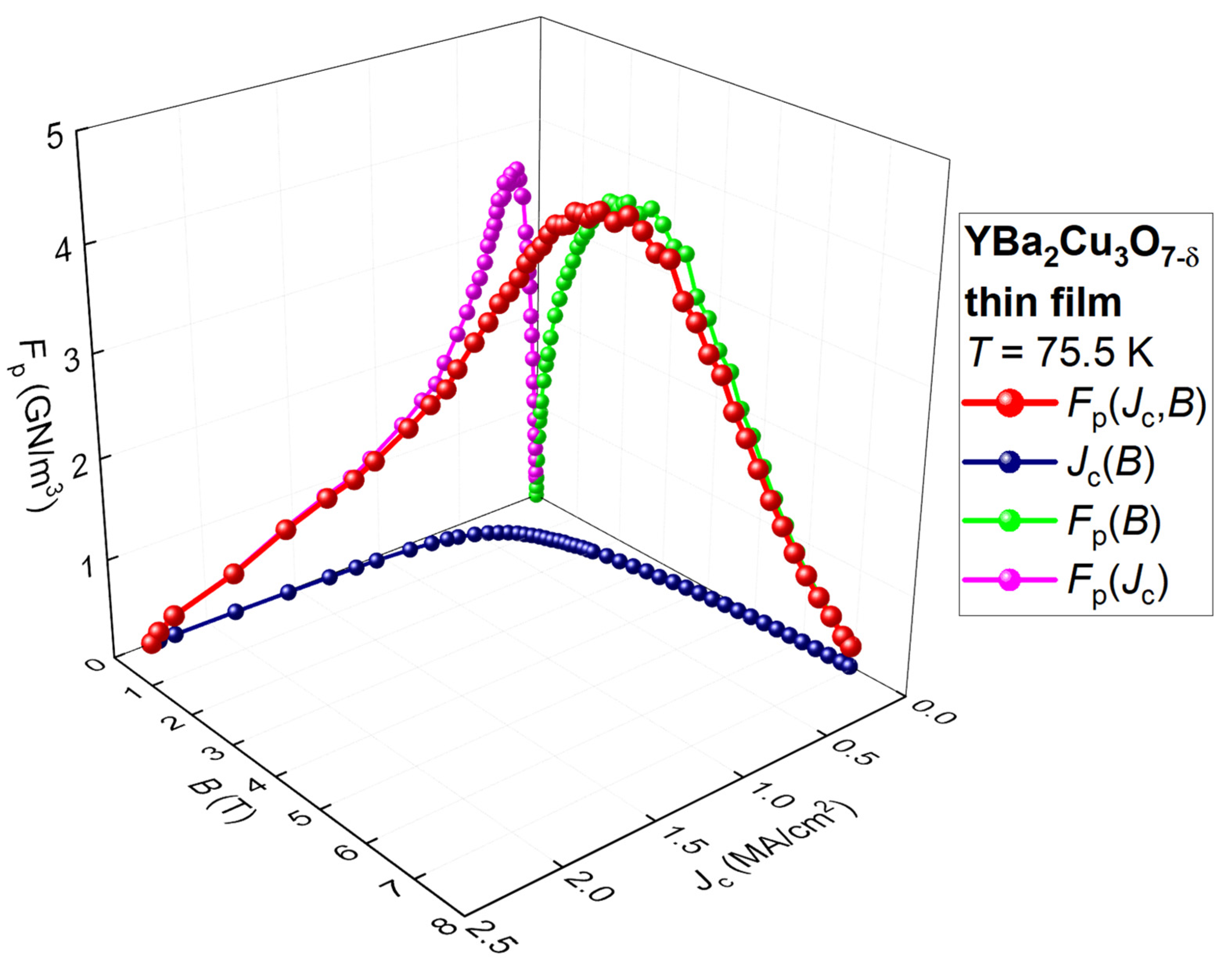
A fundamental problem for an existing approach to scale as a sole function of the applied magnetic field, B, which we found in this paper, is shown in Figure 1, where the curve for a MgB2 thin film is shown. It should be noted that raw data for these films were reported by Zheng et al. [23], and the dataset is shown in Figure 2a. Additionally, it needs to be mentioned that in all 3D representations of , we used the same axis arrangement, where X-axis is Jc, Y-axis is B, and Z-axis is .
It can be seen in Figure 1 that the curve (green), which is traditionally used for the pinning force analysis, represents a projection of the 3D curve (red) onto the X = 0 plane.
It should be stressed that at a low magnetic field, , the entire curve (red) is directed nearly in the perpendicular direction to the X = 0 plane. For this reason, the projection (green curve) of this part of the curve onto the X = 0 plane cannot be considered a correct representation of the entire pinning force density curve.
This is the primary reason for the widely accepted deduction [6,7,8,9,10,11,12,13,14,15,16,17,18,19,20,21,24,25] of the p-parameter of Equation (3), which is the primary value in Kramer–Dew–Hughes scaling laws [2,3] at :
cannot be considered to exhibit a sustainable meaning.
The geometrical representation shown in Figure 1 (where the pinning force density line is directed in a nearly orthogonal direction to the X = 0 plane) also explains why Equation (9) cannot be used to extract at a low applied magnetic field, as well the self-field critical current density, (when the applied magnetic field is B = 0 T), from the pinning force density:
where , and thus:
which contradicts with experimental observations.
It should be also mentioned that the existing theory of Abrikosov’s flux pinning [5] can be used to derive solid theoretical values for the p-parameter in Equation (3) for certain types of pinning mechanisms, defect dimensionality, vortex pinning length, and so on (see, for instance, [5]). However, it can be seen from all of the above that this parameter cannot be accepted to be a sustainable value that characterizes the pinning force density (Equation (1)) in superconductors.
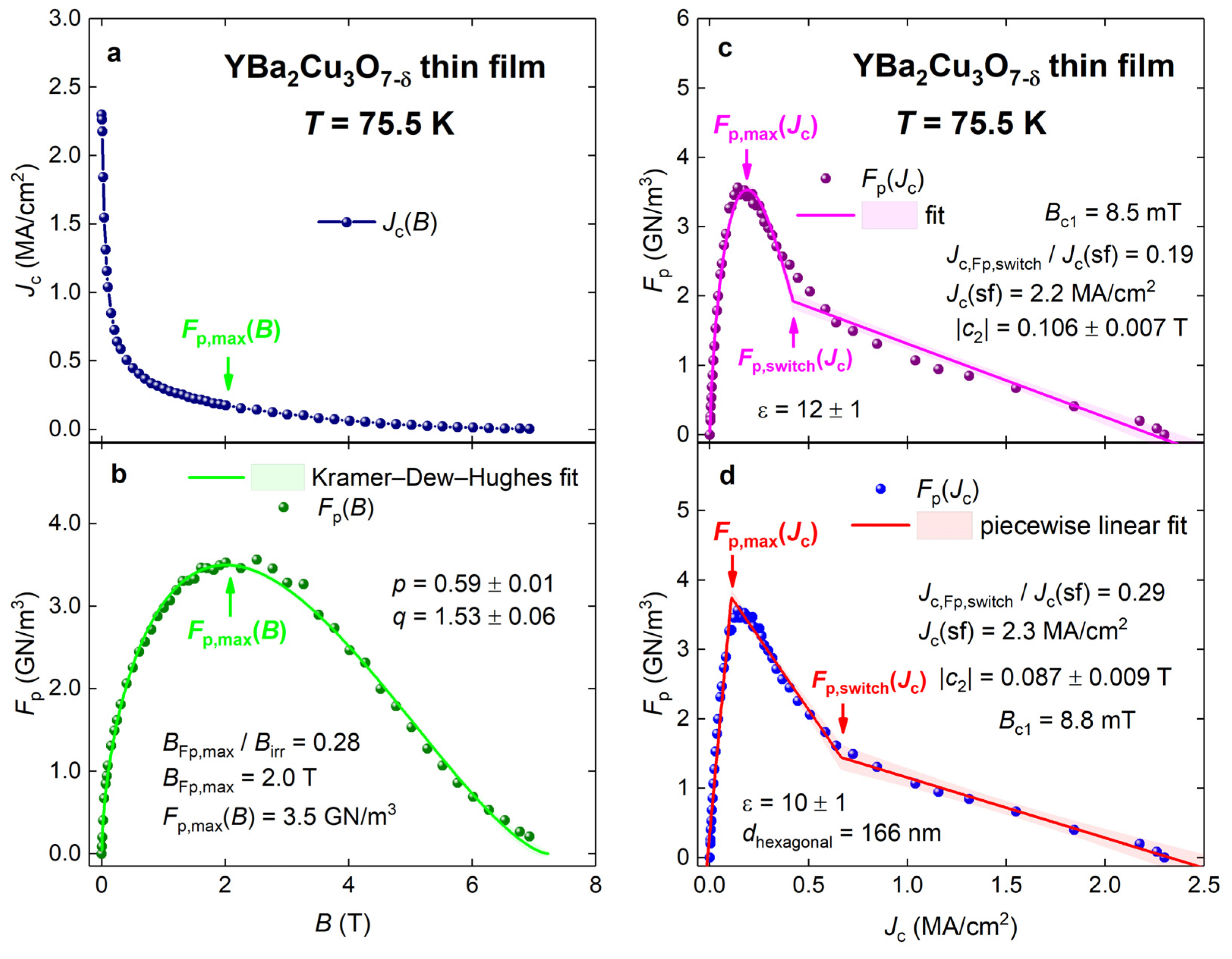
To demonstrate that the dataset for the MgB2 thin film (shown in Figure 1) represents a typical dataset for superconducting films, we fitted the projection of this dataset into the X = 0 plane, that is, to Equation (3) in Figure 2b. The deduced parameters and certainly represent typical characteristic values that are often deduced from the fits to Equation (3) [11,25,26].
It is crucial to note that this set of parameters, and , was listed by Dew-Hughes in his table ([5]), and this set of parameters implies that the flux pinning is due to the grain boundary pinning [5]. However, films fabricated by Zheng et al. [23] are epitaxial films on single crystal substrates, and thus, there is no expectation that grain boundaries are exhibited in these MgB2 thin films. However, as it is mentioned in [23], the critical current density in the MgB2 film can be governed by the grain boundaries formed by local nonstoichiometry/secondary phases, and these fine structures can act as grain boundary pinning centers at a low applied magnetic field.
Considering another projection of the 3D curve into the Z = 0 plane, which is Jc(B) (royal curve in Figure 1 and Figure 2a), we should mention that Jc(B) is largely distant from the curve, except the two points of Jc(B = 0) and of Jc(B = Bc2), where the curve intersects the plane (Figure 1). This implies that the Jc(B) projection represents the most distorted projection of the 3D curve from three orthogonal projections of this curve. Thus, if one assumes that the primary idea expressed by Anderson [1,2] is correct (i.e., that Equation (1) describes the upper limit for the dissipative-free transport current flow), then the use of the Jc(B) curve for the analysis of pinning properties of materials represents the most inappropriate choice of raw experimental data for the analysis.
Two projections of the 3D curve (i.e., and ) are in a wide use to characterize superconducting materials, and the third projection, (magenta curve in Figure 1 and Figure 2c), from the best author’s knowledge is introduced herein. exhibits a nearly linear dependence on both sides from the point (Figure 1 and Figure 2c). Based on this, for this MgB2 thin film can be approximated by a piecewise function of two linear functions:
where are free-fitting parameters and is the Heaviside function. The fit of to Equation (13) is shown in Figure 2c. Based on the deduced ratio of Figure 2c:
one can conclude a nearly full dependence; that is, the range is:
which can be approximated by a simple linear equation:
Surprisingly enough, Equation (17) is a well-known Kim model equation [27,28]. Our derivation is solely based on a 3D graphical representation of the dataset (Figure 1).
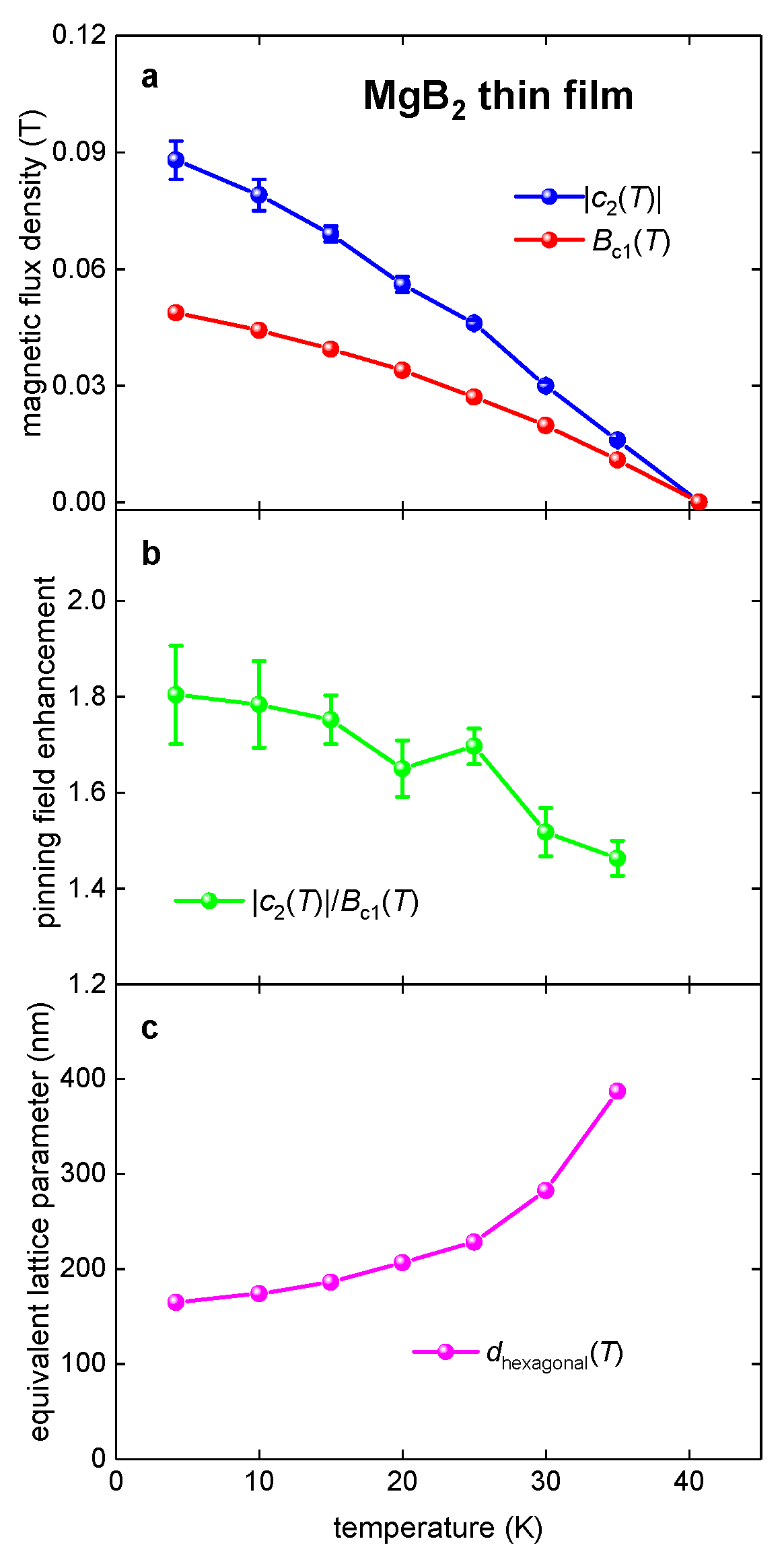
To answer the question what is the physical meaning of the t parameter in Equation (17), we first should mention that this parameter has the unit of magnetic flux density (i.e., Tesla), and that this parameter is neither nor , because its absolute value for the MgB2 film is (Figure 2), which is about two orders of magnitude below the upper critical field value. However, the latter value, which can be called the pinning field, , is comparable with (see, for instance, [29,30,31,32]), which indicates that is related to the low- and middle-field part of the curve.
Considering that is the magnetic field at which Abrikosov’s vortices have thermodynamic preference to exhibit in the superconductor, it is useful to quantify the deduced pinning field, , vs. the fundamental lower critical field of the material (at low- and middle-ranges of the applied magnetic field) by a factor of enhancement over :
Considering that the lower critical field is given by [33]:
and the self-field critical current density [34]:
one can calculate the lower limit of the pinning force density, , which can be achievable in the pinning-free thin film:
Utilizing the reported [20] and [35], one can calculate , which implies that the pinning field can be characterized by the enhancement factor . We should be clear that the applied magnetic field, for which the field was deduced, covers a wide range:
and the deduced values (i.e., and ) characterize the pinning properties of the given MgB2 film within a wide range of the applied magnetic field (i.e., low and middle applied field ranges).
From the conceptual point of view, the field can be interpreted as the so-called matching field, which is defined as the field at which each defect in the material holds one Abrikosov’s vortex. Despite intensive attempts (which were mainly focused on heavy ion irradiation of cuprates, where ion damaging tracks can be prepared in the form of continuous lines and, thus, the matching field can be calculated) [36,37,38], the matching field has been never reliably extracted from experimental Jc(B,T) data.
If this interpretation is correct, then it can be useful to introduce a characteristic hexagonal lattice parameter, , between Abrikosov’s vortices, which corresponds to the field in the assumption of hexagonal vortices’ lattice [39]:
For the given MgB2 film, the equivalent lattice parameter is , which indicates that this film is nearly pinning-site-free.
At a high applied magnetic field range, the curve (red) is directed nearly in the perpendicular direction to the Y = 0 plane. For this reason, the projection (magenta curve) of this part of the curve into the Y = 0 plane cannot be considered accurate approximation for the 3D pinning force density curve.
However, an essential difference of the projection from its orthogonal counterparts and the 3D curve itself is that the dataset always includes the origin point in the total dataset. Truly, by the definition, at at any (even for the case when the value is unknown). In Figure 2c, this origin point is depicted by the cyan color.
Overall, Figure 1 shows that the 3D curve at a low applied magnetic field is better approximated by the projection, while at a high applied magnetic field, the curve is better approximated by . These two curves are overlapped at some middle range of the applied magnetic field. The limiting values for the overlapping range can be chosen to correspond to the field values at and , shown in Figure 2d.
Thus, we can propose to split a curve in three distinctive ranges:
- Low reduced applied magnetic field range, where can be approximated by the projection;
- High reduced applied magnetic field range, where can be approximated by the projection;
- Middle reduced applied magnetic field, where and branches are overlapped and an approximation can be achieved by constructing some new function, where both branches are presented with some weights.
In next sections, we show the usefulness of this approach to analyze data for thin films of MgB2, NdFeAs(O,F), REBCO, and near-room-temperature superconducting superhydrides (La,Y)H10 and YH6. It should be mentioned that we considered only transport current datasets to avoid additional complication with the conversion of the magnetization data into the critical current density.
3. Results
3.1. MgB2
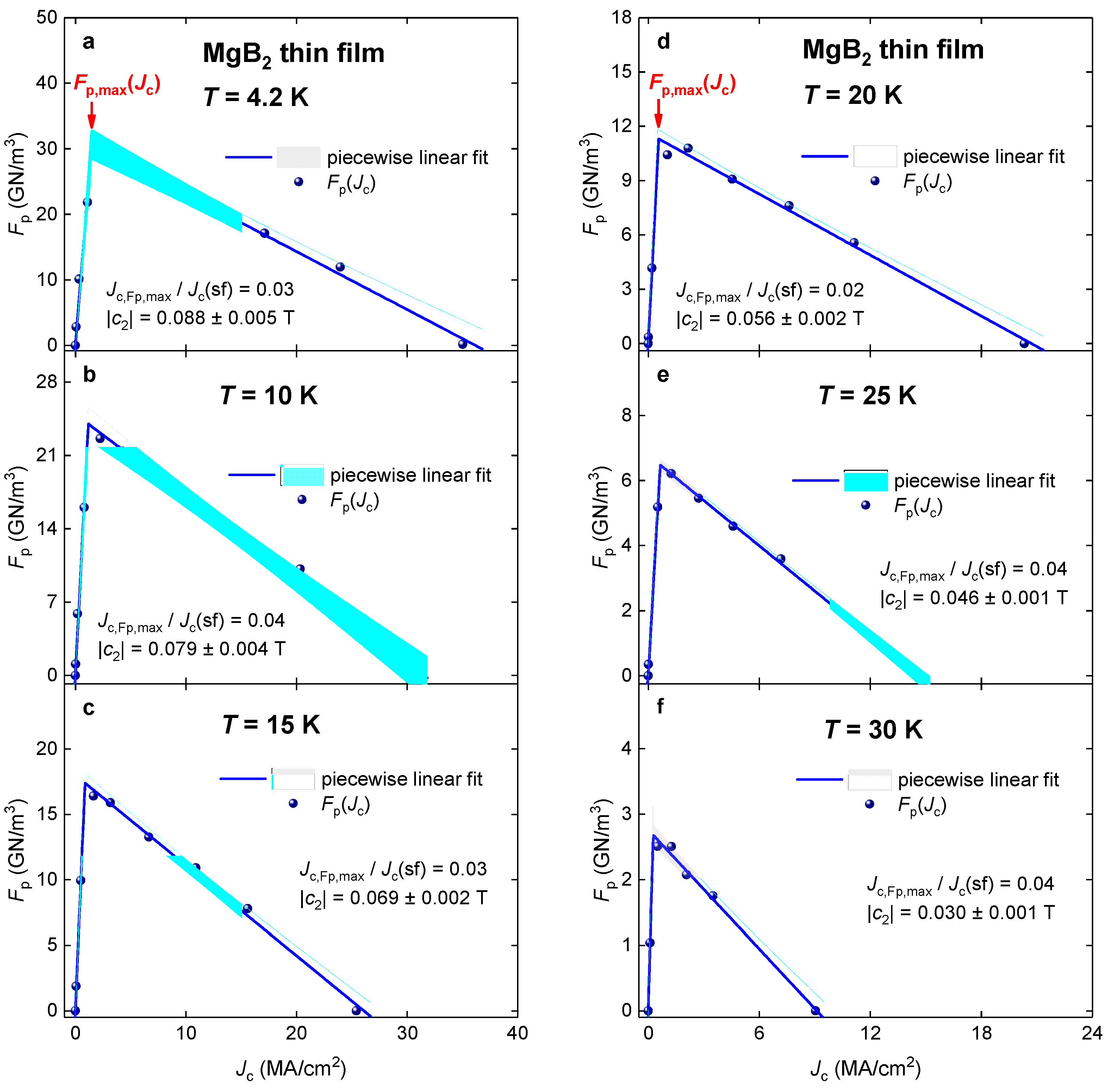
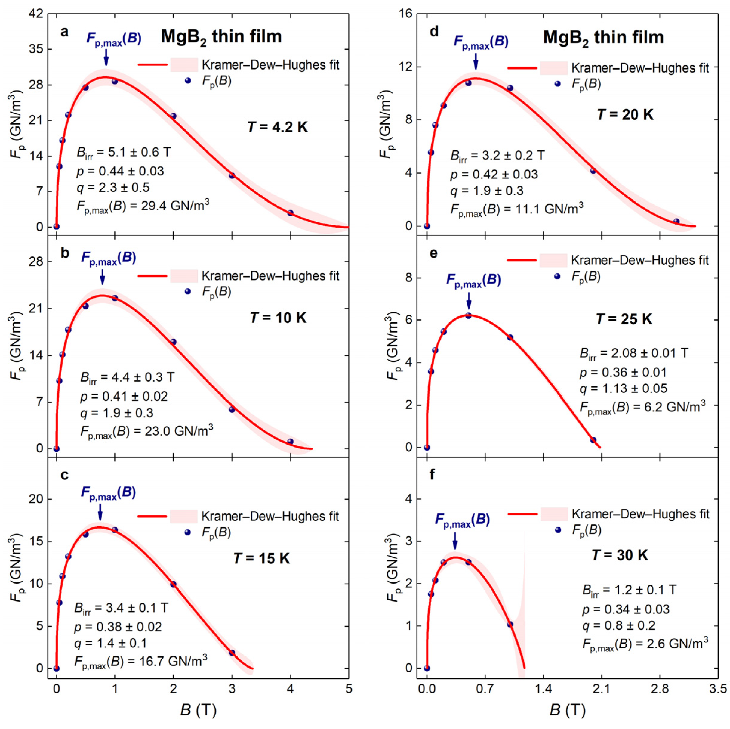
The pinning force density in pure and doped MgB2 films is studied in detail [40,41,42]. Here, we chose for the analysis the dataset reported by Zheng et al. [23], who fabricated high-quality MgB2 films by hybrid physical-chemical vapor deposition on two types of silicon carbide single-crystal substrates (4H-SiC and 6H-SiC) and reported transport datasets for the film deposited on a 6H-SiC substrate. The dataset was already analyzed in Figure 1 and Figure 2. In Figure 3 datasets measured at different temperatures are shown together with fits to Equation (13).
There are three findings revealed by the data fits to Equation (13):
This implies that the characteristic field, (Equation (13)), for the MgB2 film can be approximately scaled as the lower critical field, , for this material.
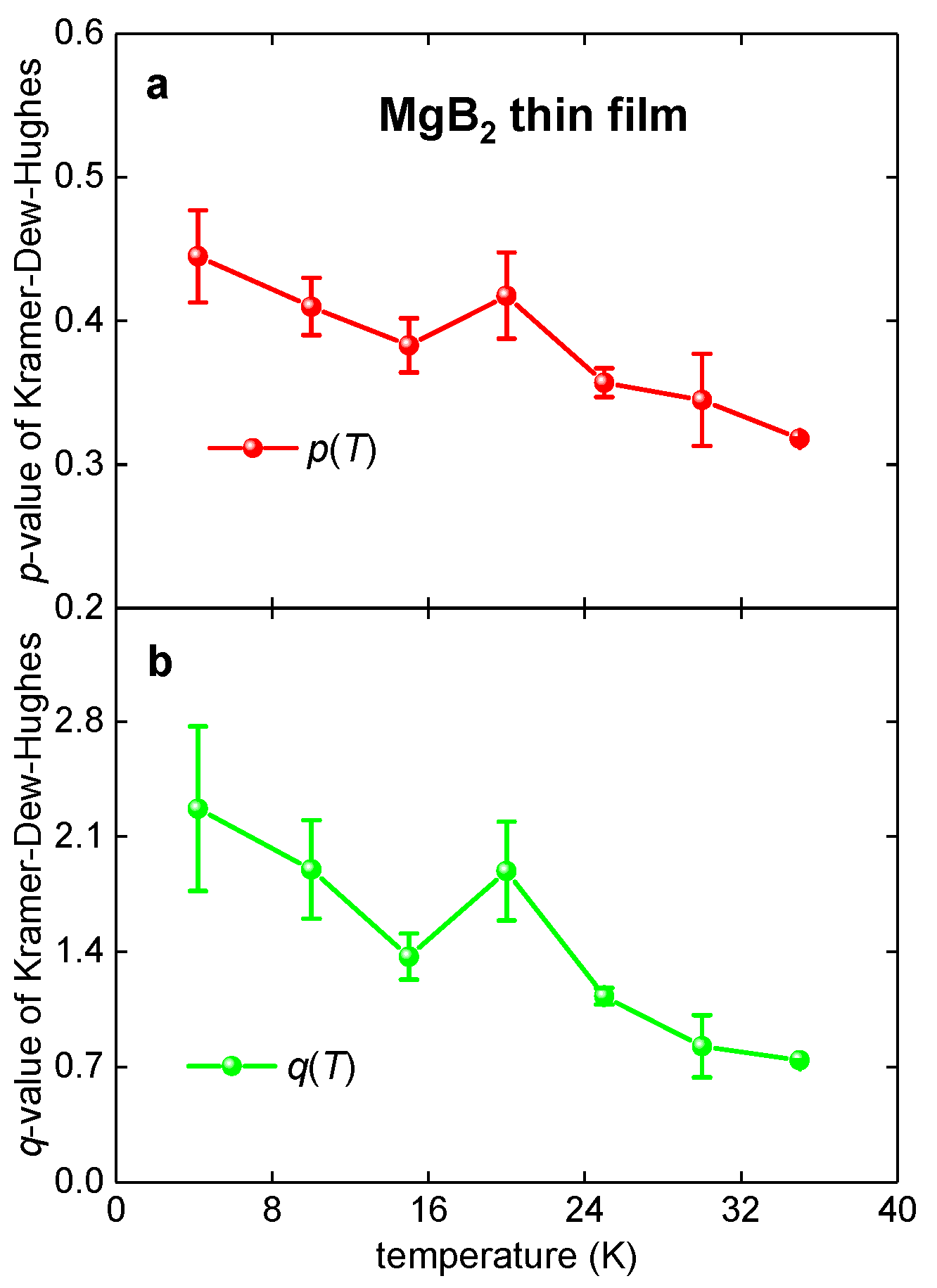
The data fits to Equation (3) and deduced parameters are shown in Figure 5 and Figure 6, respectively. It can be seen (Figure 6) that both deduced parameters, p(T) and q(T), are varying within very wide ranges, which were not described by Dew-Hughes [5]. Moreover, the p(T) and of q(T) parameters deduced at different temperatures indicate different pinning mechanisms. For instance, and , which imply that the pinning is due to magnetic/volume/normal mechanism [5], while and , which imply that the pinning is due to the core/surface/normal mechanism [5]. This result demonstrates that the Kramer–Dew–Hughes [4,5] model exhibits a problem with the validity of deduced value interpretation, while mathematical fits to Equation (3) are, as a rule, reasonably accurate approximated data.
3.2. Pnictide Thin Films
In this section, the analysis was applied for two NdFeAs(O,F) thin films for which raw transport critical current density data, , were reported by Tarantini et al. [43] and Guo et al. [44]. Both research groups found that the data fit to Equation (3) generates unphysical and values, which was interpreted as a demonstration of a superposition of two different pinning mechanisms. To resolve this problem, Tarantini et al. [43] proposed to fit datasets to a function that is a sum of two Kramer–Dew–Hughes functions, where one function accumulates the contribution of the surface pinning (for which and in accordance with 5) and another function accumulates the contribution of the point pinning (for which and in accordance with [5]):
A slightly different approach was proposed by Guo et al. [44], who considered that two summation parts in Equation (26) have , and thus, these authors proposed to use the following fitting function:
where p is free-fitting parameter. Because the surface pinning is characterized by and the point pinning is characterized by [5], the proximity of the free-fitted p-value to either 0.5 or 1.0 can be interpreted as the dominance of the surface pinning or the point pinning.
In the results, both research groups [43,44] reported that the point pinning dominates at , while at , the dominant mechanism is the surface pinning. Because the comprehensive analysis of for NdFeAs(O,F) thin films was reported in [43,44], here, we only presented an analysis for the datasets.
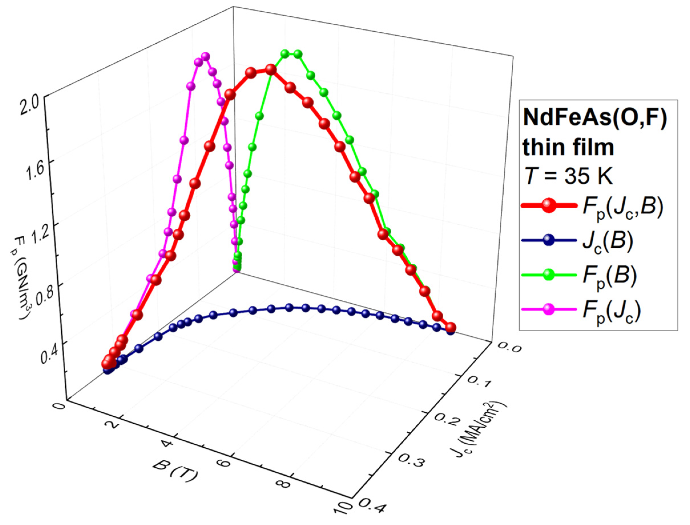
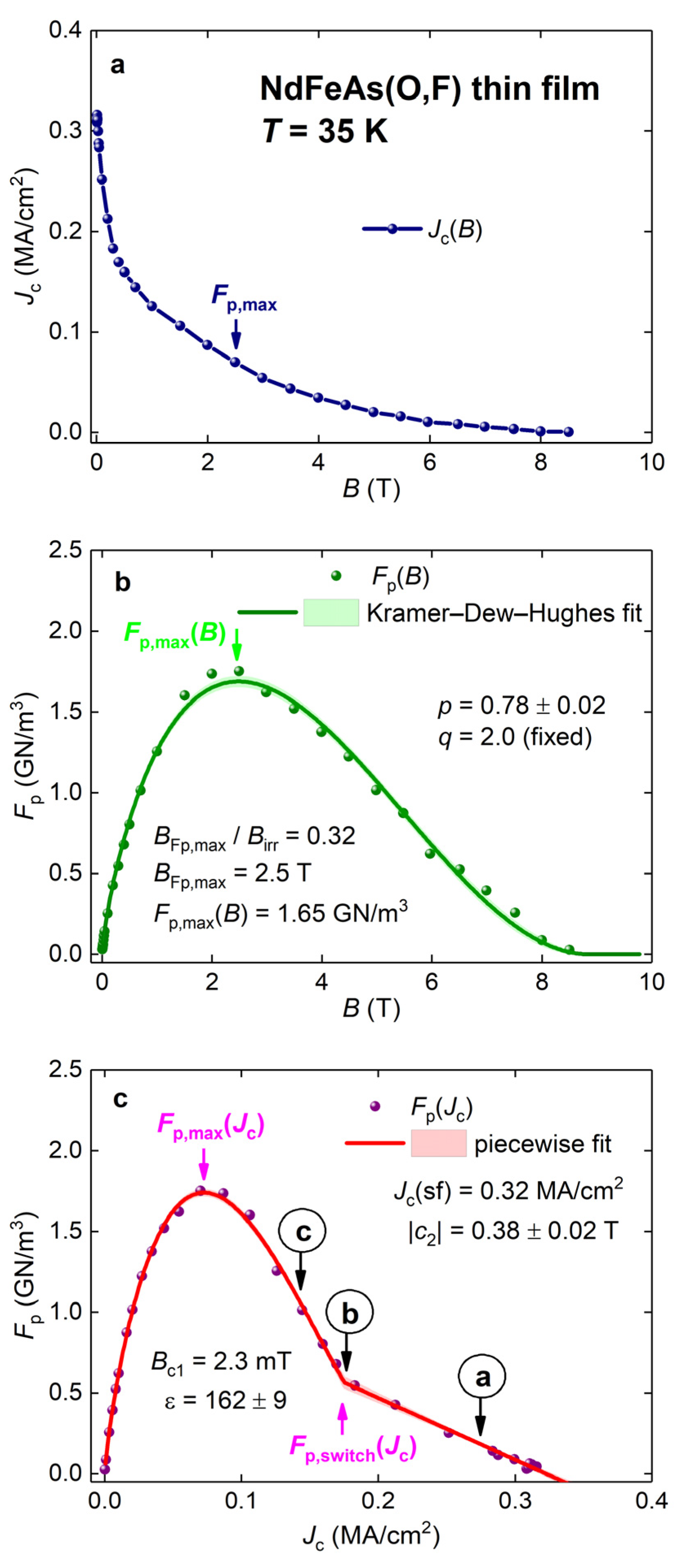
In Figure 7, we show the dataset for the NdFeAs(O,F) thin film for which was reported by Guo et al. [44].
A curve (green) can be fitted to Equation (26) with high quality (Figure 8). However, on this projection, an important property of the dataset, which is a linear dependence of (Figure 7 and Figure 8c), is invisible.
Another important feature, which makes the curve for the NdFeAs(O,F) thin film different from its counterpart for the MgB2 film (Figure 1 and Figure 2), is that the low-field linear part of the curve abruptly transforms into a domelike shape of at the point. This important feature is also invisible in the projection of the curve (Figure 8b).
One can see in Figure 7 and Figure 8 that the 3D curve starts to deviate from the projection when . For , the 3D curve is better approximated by the projection. The fitting function for the domelike part of the curve should be flexible within the full range of . We constructed several possible functions and found that the general form proposed by Kramer [4] and by Dew-Hughes [5] can reasonably well fit data:
where , , , , , and are free-fitting parameters. It should be stressed that because (as one can see in Figure 1 and Figure 7) the projection of the 3D curve into the B = 0 plane is significantly distorted from its original 3D curve, when . Additionally, the fit to Equation (28) can be a good approximation for values within the range of .
Thus, there is an interesting analogy with the Kramer–Dew–Hughes fit (Equation (3)), which is a reasonably accurate approximation for the curve for large applied magnetic fields, that is, within a range of , while Equation (28) is a good approximation for for large critical current densities, , or what is the equivalent statement, for low- and middle-range applied magnetic fields .
However, we can note that Equation (28) has a linear part, which represents a significant difference between Equations (3) and (28). In addition, as we stated above, there is a need to revise the validity of the primary interpretation of the p and q parameters in the Kramer–Dew–Hughes fit, which was proposed by Dew-Hughes nearly five decades ago [5]. Based on this concern, we do not provide any interpretation for the l and m parameters in Equation (28) now.
To interpret the physical origin of the appearance of the domelike bump in the datasets (Figure 9), which suddenly appeared at (Figure 8c), we can propose that this dome is due to the effect of Abrikosov’s vortices’ collective pinning [45]. This effect was theoretically predicted by Larkin and Ovchinnikov more than five decades ago [45], and despite a wide discussion of this effect in cuprates [46], to the author’s best knowledge, Figure 8 represents clear experimental evidence for the existence of this effect. This interpretation is well aligned with the absence of the collective pinning in MgB2, and thus, Figure 1, Figure 2 and Figure 3 demonstrate that the domelike bump in the datasets does not exist.
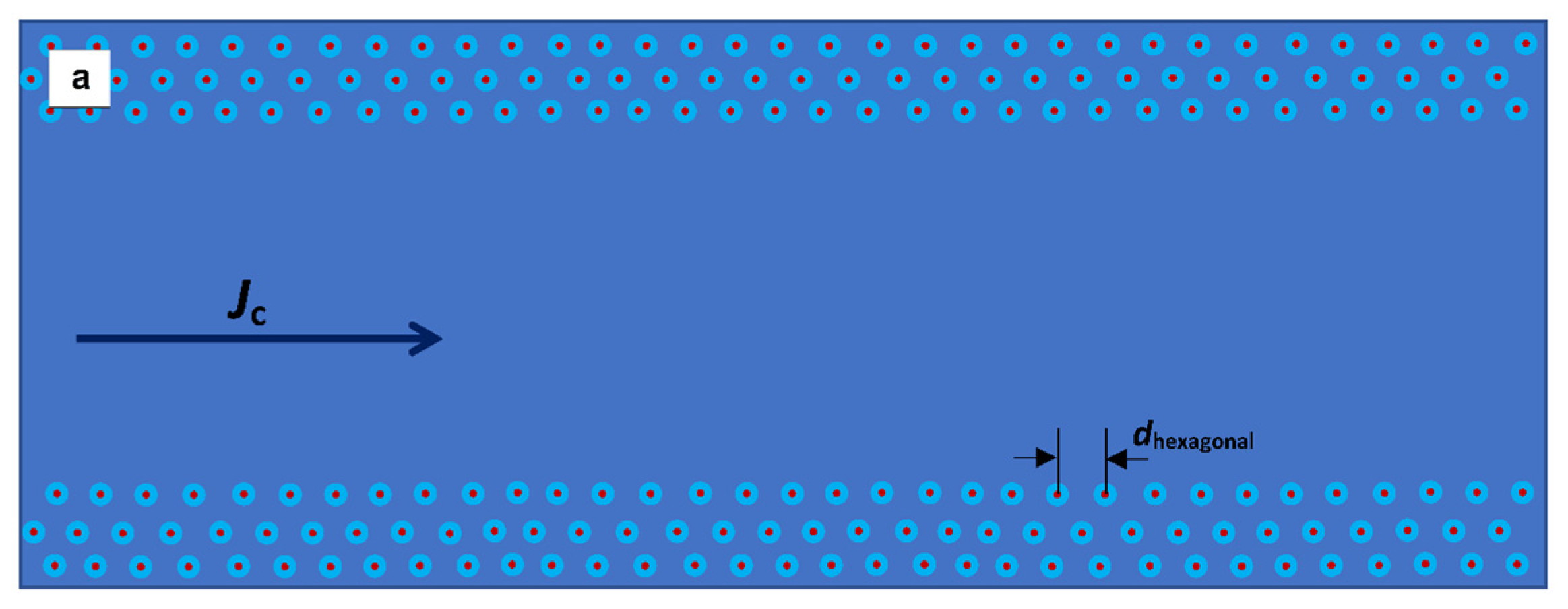
Following a general idea for the magnetic flux distribution in a thin superconducting slab when the external magnetic field is applied in the perpendicular direction to the film surface proposed by Brandt and Indenbom [47], in Figure 9, we show a schematic representation for vortices’ lattice for three distinguishing parts of the curve, which can be seen in Figure 8c. At a low applied magnetic field, that is, , Abrikosov’s vortices fill the superconducting film starting from the slab edges and vortices separated by the distance, , which corresponds to the field (Equation (23)). This stage corresponds to the linear part of the curve indicated by the letter “a” in Figure 8c.
The vortices completely and uniformly fill the film at the applied field of , while the distance between vortices remains to be (Equation (23)). This stage is indicated by the letter “b” in Figure 8, and the schematic diagram is shown in Figure 9b.
At the applied , there are two possible scenarios. One is for materials such as MgB2, which do not exhibit the collective flux pinning effect, and after the applied field reaches , the pinning force density is rapidly dropped (see, for instance, Figure 3). Otherwise, if a material exhibits the collective flux pinning effect, Abrikosov’s vortices penetrate in the slab from the edges and form the second flux penetration front, which has a much higher fluxon density and does not exhibit a hexagonal flux lattice structure.
The fit of the dataset to Equation (28) and calculations based on Equations (18), (21) and (23) reveal the following values (for calculations, we used the Ginzburg–Landau parameter [48]):
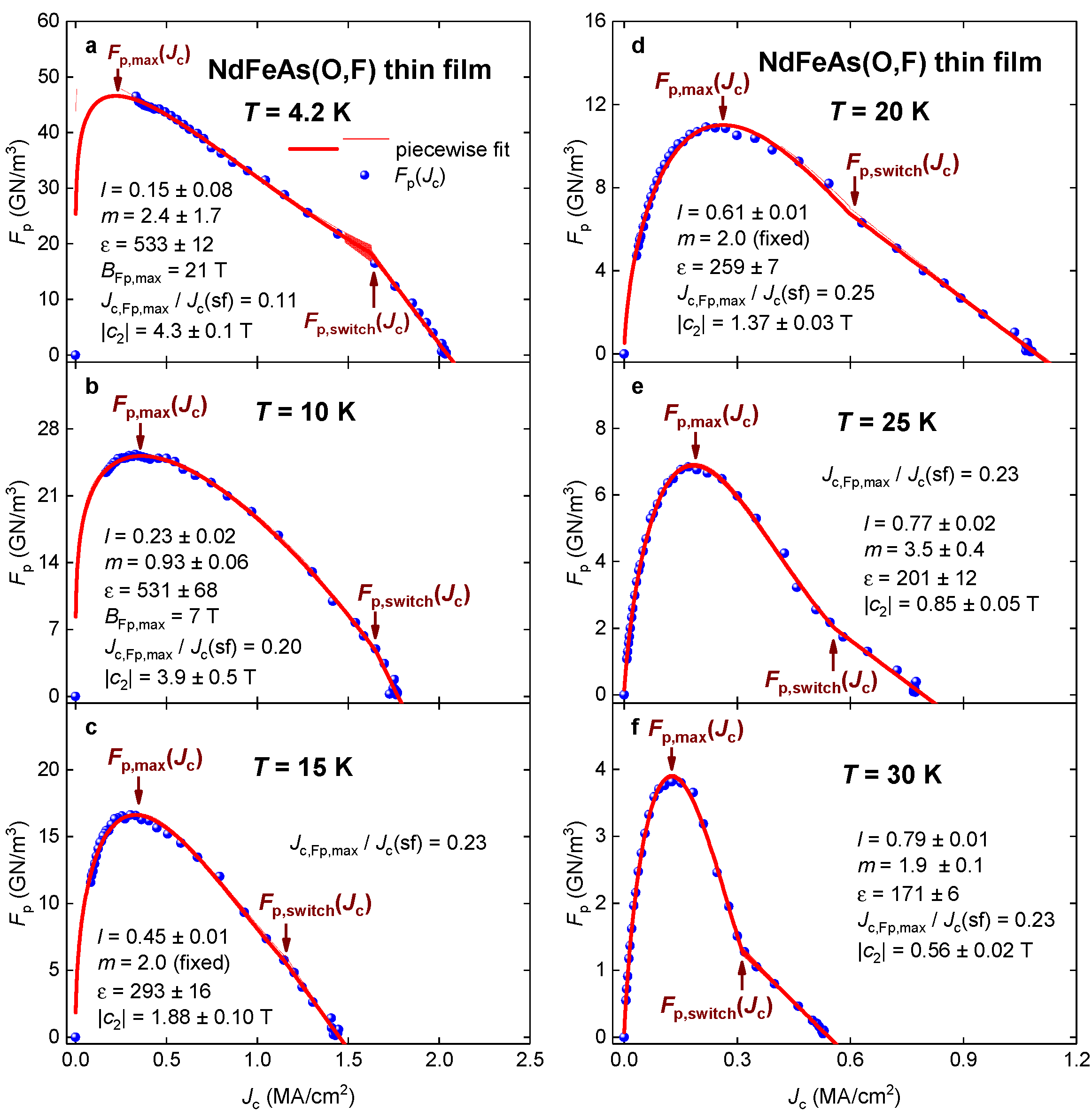
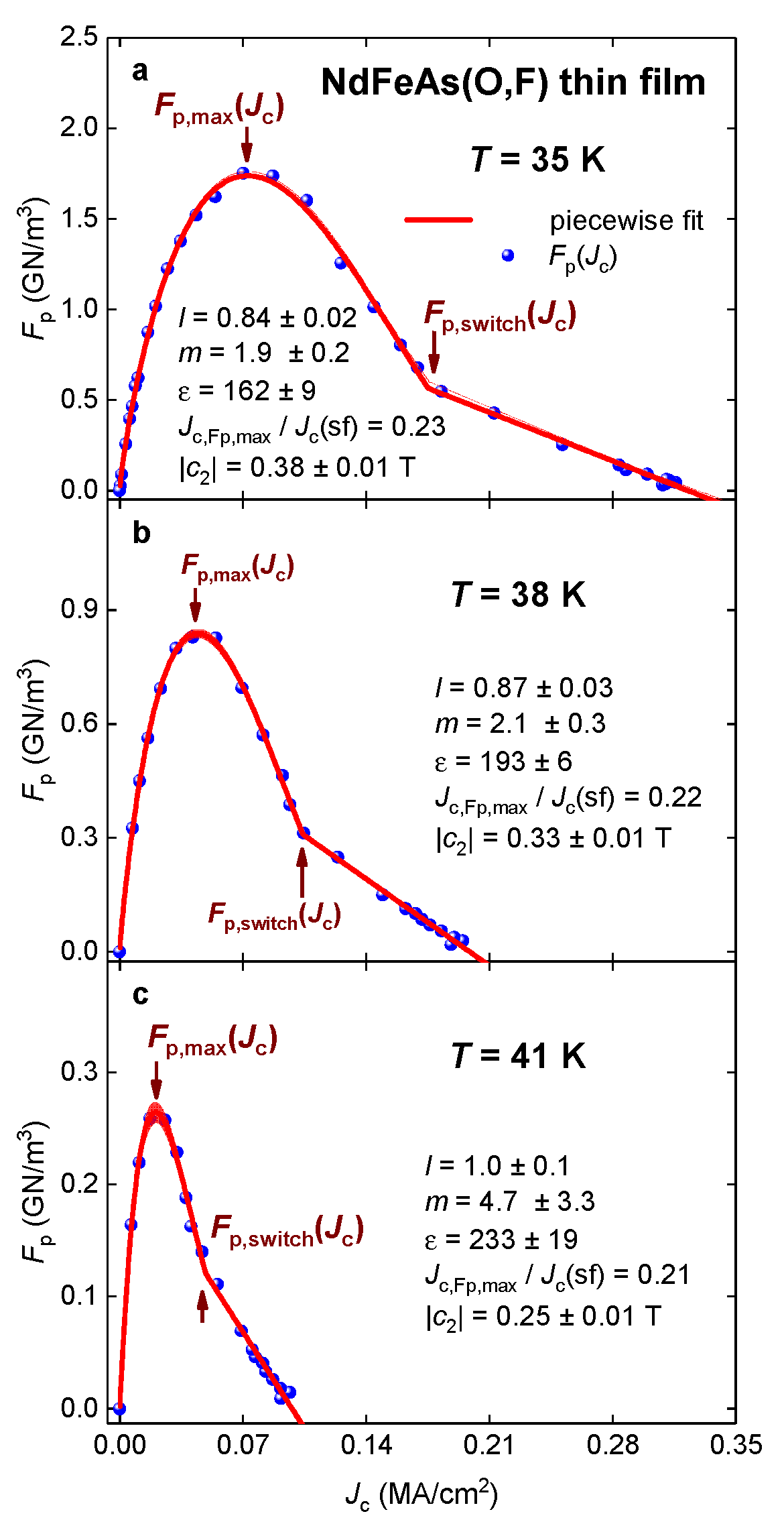
Fits to Equation (28) of datasets measured at different temperatures for the NdFeAs(O,F) thin film are shown in Figure 10 and Figure 11.
Overall, datasets measured at high reduced temperatures, , have a very pronounced linear part (Figure 11). When the datasets do not contain large-enough raw data points to be fitted to Equation (28) (for all parameters are free), we fix the value, adopting the approach proposed for NdFeAs(O,F) thin films in [38,39]. The primary reason for this is that our purpose is to extract as accurately as possible the value, which is the slope at a low applied magnetic field. Based on this, the accuracy of the approximation of the collective pinning peak in cannot be characterized as our primary task, because we target to deduce the values listed in Equations (29)–(32), for which parameters describing the collective pinning bump are not required.
It is important to note that all fits to Equation (28) of all reported (by Guo et al. [44]) datasets were converged, which is a prominent advantage versus datasets fit to Equation (5), where the converging is the main issue, especially for datasets measured at low temperatures.
The converged curve can be inverted to calculate the important pinning parameter , which cannot be extracted from datasets, because the latter dependences, as a rule, at T ~ 4 K for all practically important materials (i.e., cuprates and IBS) are an increasing function of B. Based on this, the fits to Equation (3) diverge.
However, if the same dataset is to be projected into the B = 0 plane (which is ), it can converge, as is demonstrated in Figure 10a. Because the curve, as we mentioned above, is an accurate approximation for the 3D curve for , the deduced from the converged fit to Equation (28) can be a reasonably accurate estimation for . To perform this inversion of the fitted curve for the NdFeAs(O,F) film (Figure 10a), one obtains , which is significantly above the highest applied magnetic field in the given experiment, [44].
Primary deduced parameters are shown in Figure 12. There are remarkable high values for the pinning field enhancement factor, , within a full temperature range. This is the most distinguished difference in values deduced for the NdFeAs(O,F) thin film in comparison with MgB2 (see, for instance, Figure 4 and Figure 12).
3.3. REBCO Thin Films
The introduction of nanoscaled secondary phases (so-called artificial pinning centers (APC)) in REBCO thin films is a conventional approach to enhance the in-field critical current density, , which was introduced nearly simultaneously by MacMagnus-Driscoll et al. [49] and Haugan et al. [50]. However, there are a growing number of pieces of experimental evidence [22,51] that a prominent enhancement exhibits only at a high reduced temperature range, that is, at , while at , the enhancement originated from APC and 124-stacking faults practically vanishes [22,51].
In attempts to develop a better understanding of this problem, which has a great practical importance [52], we analyzed data for REBCO thin films by the approach described above.
In Figure 13, we show a 3D data curve for an undoped YBa2Cu3O7-δ thin film (Sample 87) reported by MacMagnus-Driscoll et al. [49] (it should be noted that in Figure 1b [49] (from which data were digitized), the Y-axis has a mistake in value numbering).
Three orthogonal projections of the curve are shown in Figure 14, where one can see that the fit to Equation (3) of the dataset has a high quality. However, a linear dependence of (Figure 13 and Figure 14c,d), which covers a significant part of the range, cannot be recognized in the projection.
The fit of the dataset to Equation (28) is shown in Figure 14c, where the m parameter was fixed to . However, a more accurate approximation of the linear part and the full curve is achieved by using a three-step linear piecewise function:
The fit is shown in Figure 14d.
Equation (33) represents one of the simplest and, simultaneously, remarkably accurate mathematical expressions of our primary idea that has three distinctive ranges (which we already mentioned above, but it is important to list these ranges again), each of which can be approximated by a linear curve:
- Low reduced applied magnetic field range, where the approximation is the line (which corresponds to the schematic diagram shown in Figure 9a);
- High reduced applied magnetic field range, where the approximation is the curve;
- Middle reduced applied magnetic field, where the line and curve can be approximated by a median curve or line.
Calculations based on Equations (21), (23) and (33) reveal the following values (for calculations, we used the Ginzburg–Landau [39,53]):
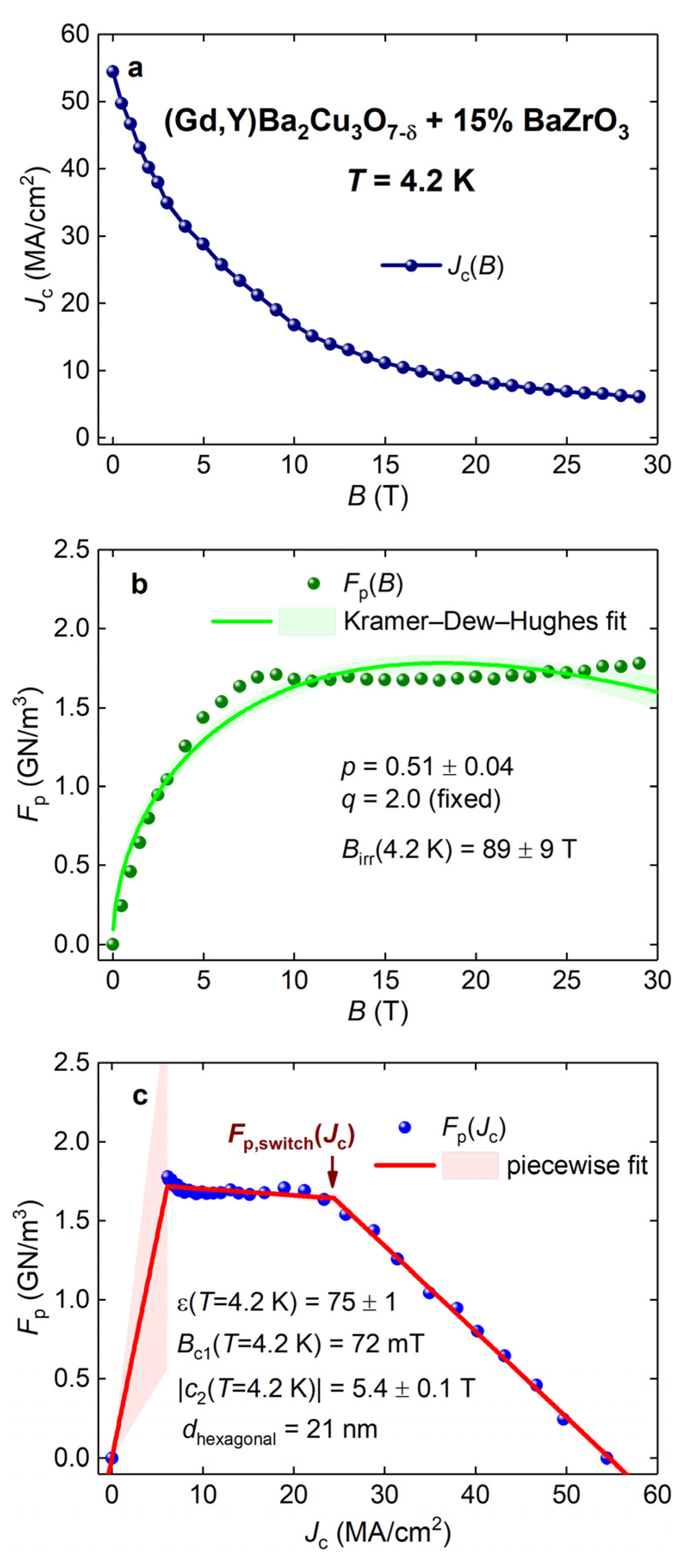
Before we present the results of the analysis of the temperature dependence of the datasets for one of a few commercially available HTS 2G-wires, it will be interesting to present the data analysis for a laboratory-made sample, which can be considered as the upper limiting case for commercial HTS 2G-wires. Xu et al. [54] fabricated and studied a ∼0.9 μm thick (Gd,Y)Ba2Cu3O7-δ + 15% BaZrO3 thin film, which was deposited on a standard buffered IBAD Hastelloy substrate by the metal–organic chemical vapor deposition technique. The and datasets are shown in Figure 15a,b, respectively (datasets are reported in [54]). It should be mentioned that the fit to the Kramer–Dew–Hughes model, despite that it converged at a fixed q =2.0 value, does not have high quality.
However, the fit of the dataset to Equation (33) has converged (Figure 15c), and the linear dependence of at high critical current densities is remarkably clear and accurate. It should be stressed that there are no visual designations in either Figure 15a or Figure 15b that there is a very sharp transition between two linear dependences in , which can be observed clearly in Figure 15c at .
Calculations based on Equations (21) and (23) reveal the following values (for calculations, we used the Ginzburg–Landau [53]):
There are two good matches between deduced values (Equations (38)–(41)) and reported values. The first one is deduced , which is in good agreement with reported values for YBa2Cu3O7-δ single crystals [55,56].
The second agreement with that reported by Xu et al. [54] is the average distance between BaZrO3 nanorods in the REBCO matrix, which was extracted from the analysis of transmission electron microscopy (TEM) images, [54]. We deduced the equivalent hexagonal vortex lattice parameter (Figure 15 and Equations (23) and (33)). These two characteristic lengths can be considered equal, because the natural variation of the BaZrO3 nanorod density in the REBCO matrix has reasonable variation, even within the viewing area of the same TEM image (see, for instance, Figure 10 in [15]).
Thus, there is the first direct experimental evidence that the field can be interpreted as the matching field related to the density of structural defects in superconductors.
We should stress that the field is not a field at which the or curves have any sort of inflection or other unique features, because the field is the linear coefficient between and at a low reduced applied magnetic field, . Perhaps this is the primary point, which designates our approach and all previous attempts to define the matching field. This means that is the characteristic field that quantified the pinning strength of the superconductor within a wide range of the applied magnetic field, B. This is not a threshold field at which some or any designated features in the and curves can be observed. The analogy here can be similar to the behavior of Jc(B) at B = BFp,max (where BFp,max is the applied field at which the pinning force density reaches its maximum) because Jc(B) represents a smooth function at B = BFp,max and there is no feature that can manifest that the applied field equals the BFp,max, until some mathematical operations will be applied to Jc(B).
In this regard, represents an integrated linear response of the pinning landscape of the superconductor on the applied magnetic field, from which the characteristic hexagonal lattice parameter, , at which Abrikosov’s vortices are separated, can be calculated.
This is obvious, but an important issue, that is not a field at which the inflection in the curve (i.e., ) is observed. On the other hand, it might be useful to perform detailed experimental studies of and in a variety of superconductors.
It is interesting to note that deduced (Equation (41)) for the (Gd,Y)Ba2Cu3O7-δ+15% BaZrO3 film is in the same ballpark with for the NdFeAs(O,F) film, which we deduced above (Figure 12).
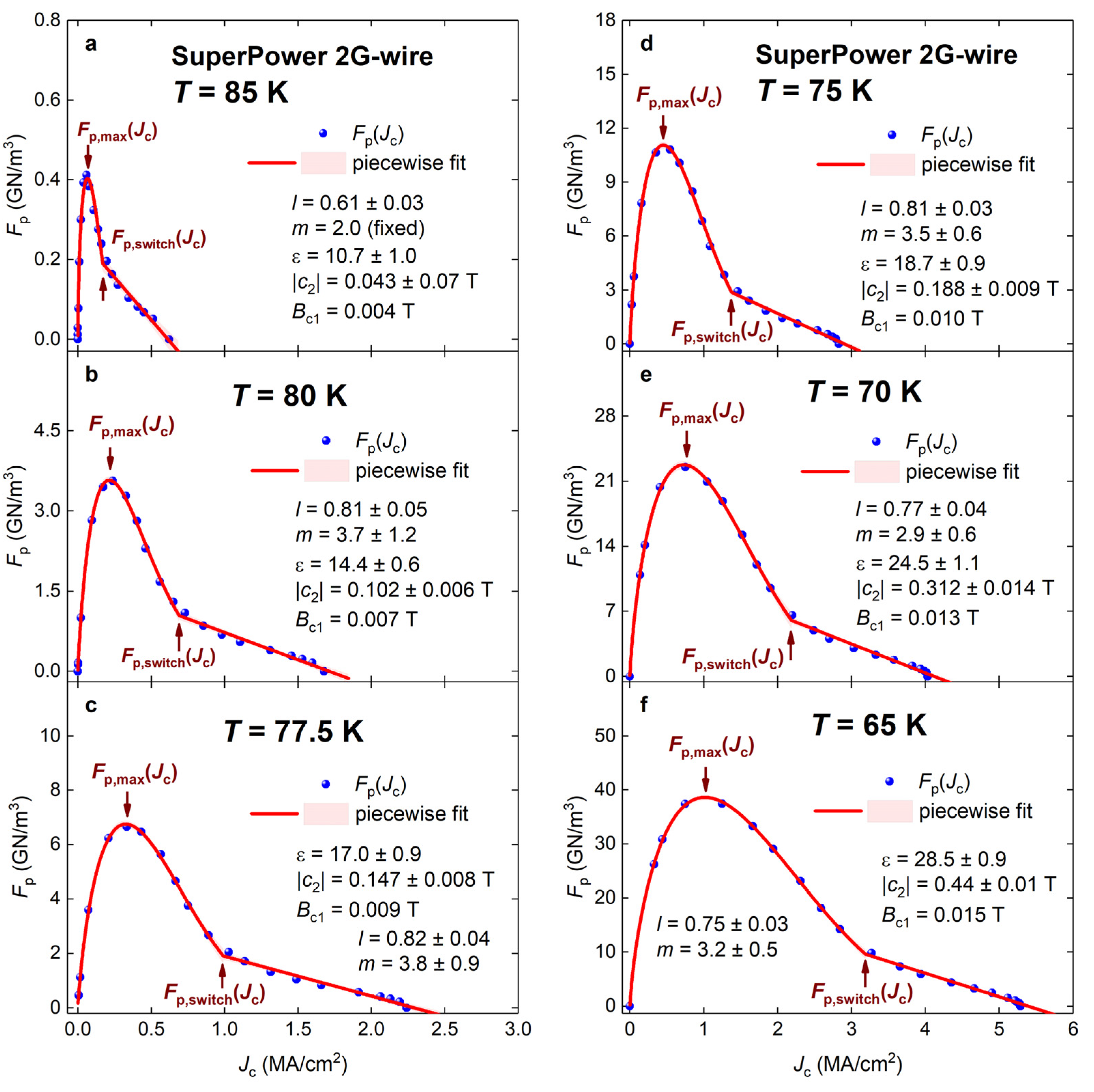
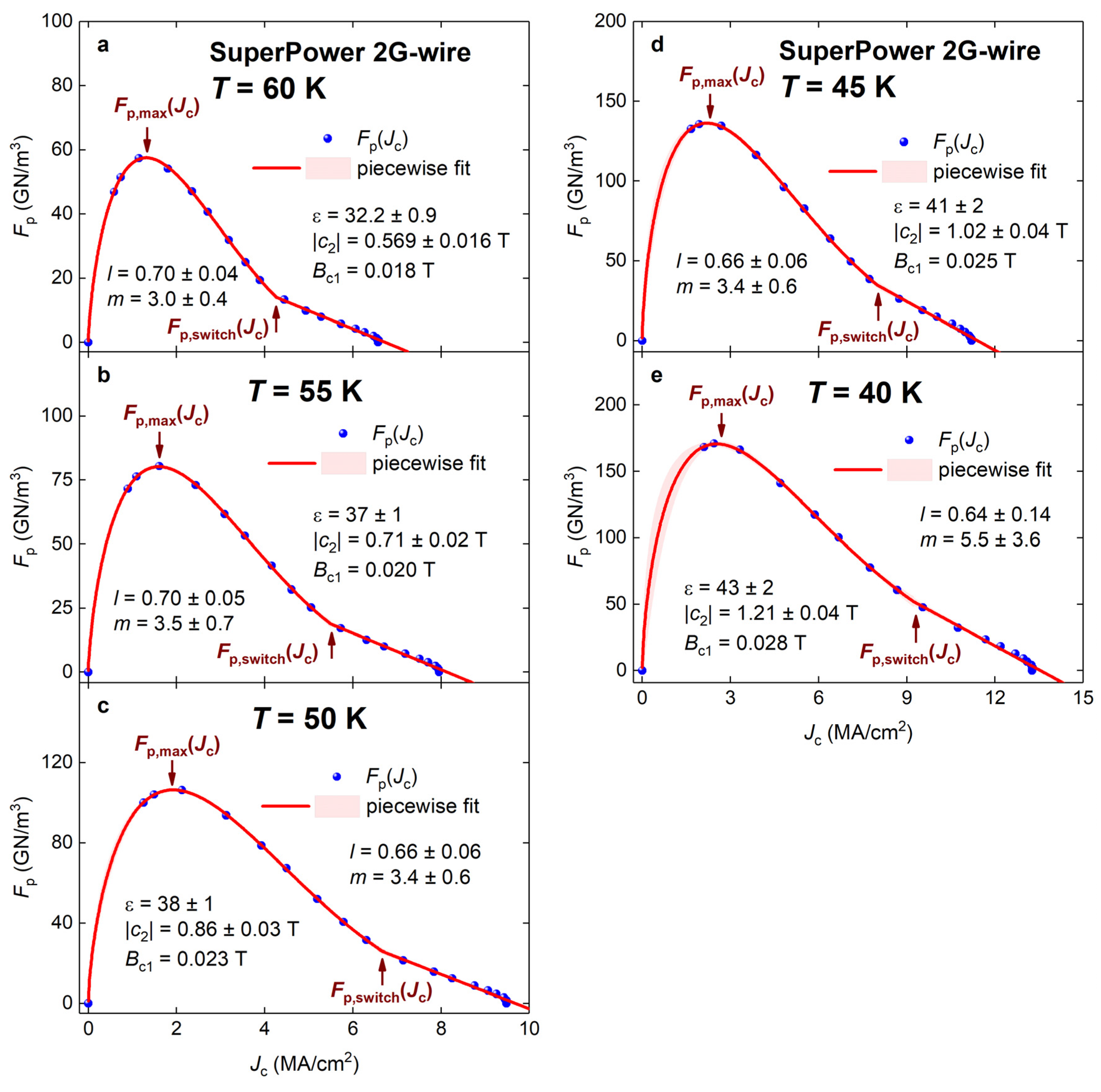
To demonstrate the applicability of our approach to analyze commercial HTS 2G-wires, in Figure 16 and Figure 17, we show that the analysis for SuperPower Inc. wire (raw experimental data is available online at an RRI high-temperature superconducting (HTS) wire critical current database [57]). To perform the analysis, we assumed that the REBCO film has a thickness of 1.7 μm, and all datasets were fitted to Equation (28).
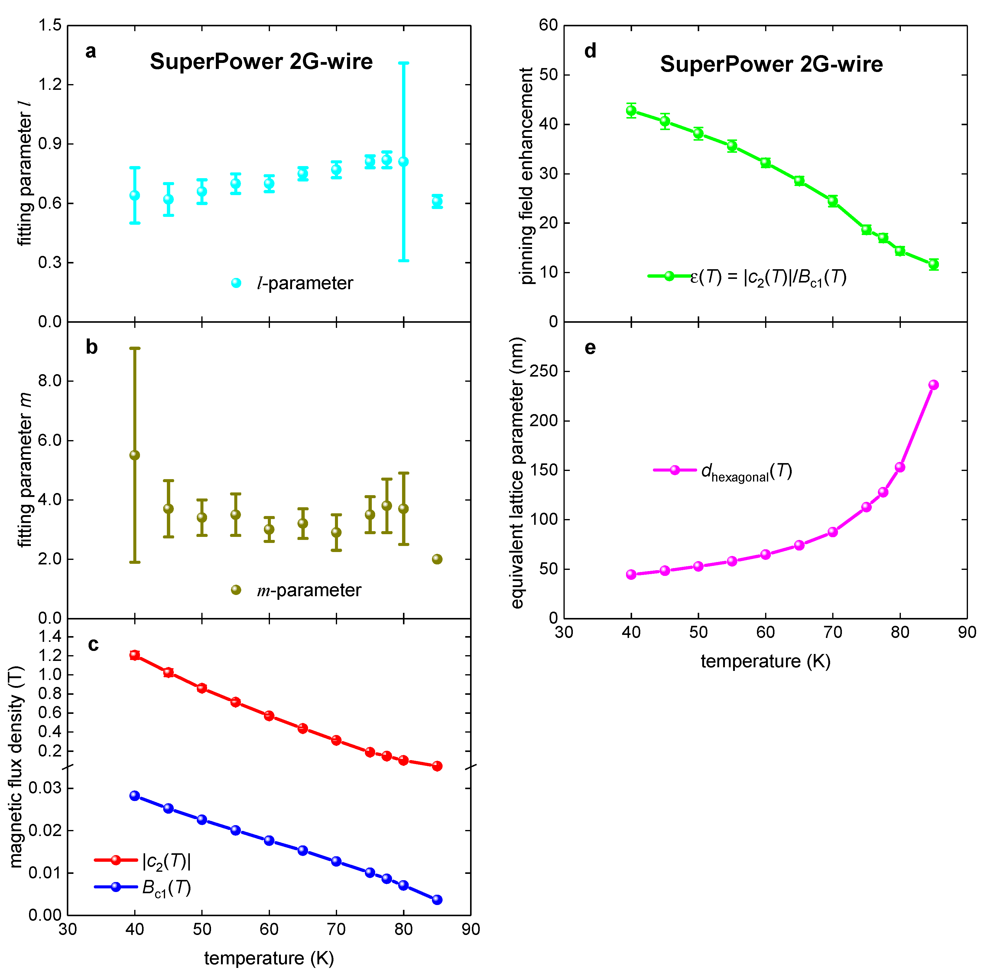
Deduced parameters are shown in Figure 18. Overall, the deduced pinning field enhancement factor, ε(T) (Figure 13, Figure 14, Figure 15, Figure 16 and Figure 17), in REBCO superconductors is varying within the range:
These values of are in times lower than in the NdFeAs(O,F) thin film (Figure 12).
The collective pinning peak is observable in all curves shown in Figure 14, Figure 16 and Figure 17. We should also note that there is a general similarity in the shape of measured in the NdFeAs(O,F) film (Figure 10a) and (Gd,Y)Ba2Cu3O7-δ + 15% BaZrO3 film (Figure 15c), because both curves have a steep linear raise of at low applied magnetic fields.
3.4. Near-Room-Temperature Superconductors (La,Y)H10 and YH6
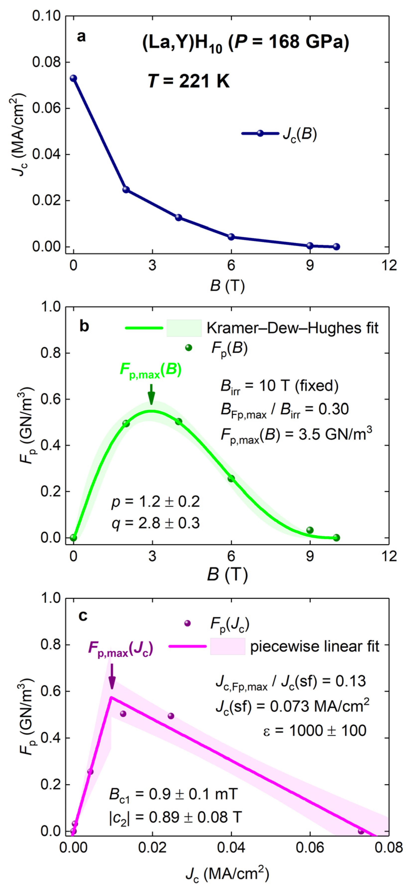
An astonishing experimental discovery of near-room-temperature superconductivity (NRTS) in highly compressed H3S by Drozdov et al. [58] sparked a worldwide research initiative in the hydrogen-rich superconductivity [59]. Recently, Semenok et al. [60] predicted NRTS in ternary hydride (La,Y)H10 by first-principle calculations and consequently synthesized this ternary hydride, which exhibited up to 253 K, depending on the applied pressure. Semenok et al. [60] reported an in-field transport critical current, , dataset for (La,Y)H10, which exhibits zero resistance Tc = 233 K at pressure P = 186 GPa.
Here, we analyzed and R(T) data for the (La,Y)H10 sample compressed at P = 186 GPa (for which raw data are shown in Figure 4 in [60]). By assuming a sample thickness of 1 μm and a sample width of 20 μm, , , and were calculated, and these datasets are shown in Figure 19. We also added in these datasets an experimental value for (which can be extracted from data shown in Figure 4b in [60]).
The most impressive deduced value for the (La,Y)H10 sample is the pinning field enhancement factor, , which exceeds its counterpart in the IBS NdFeAs(O,F) film (for calculations, we utilized the Ginzburg–Landau parameter , deduced for highly compressed H3S [61]):
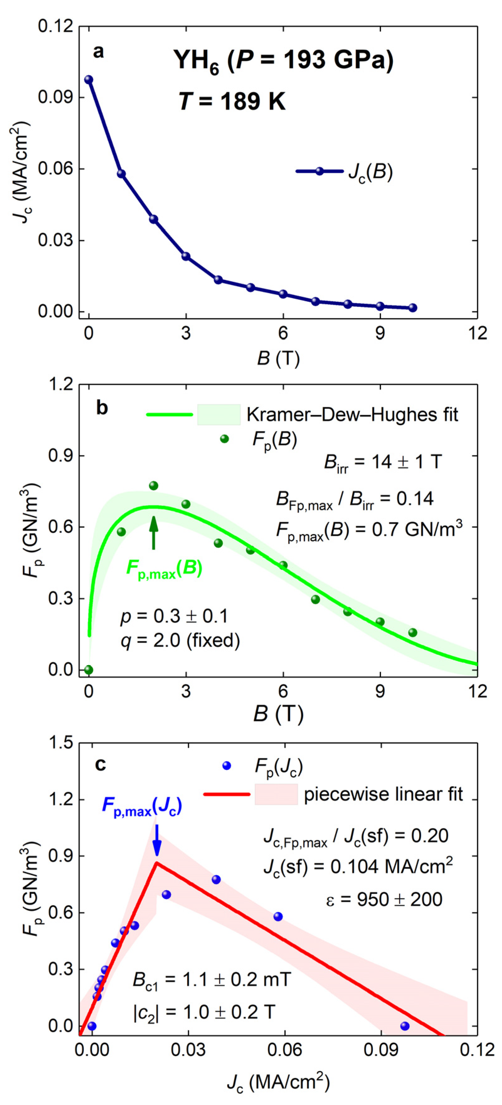
In attempts to confirm this result, we analyzed an in-field transport critical current, , dataset for another NRTS superconductor, YH6, which was simultaneously discovered by Troyan et al. [62] and Kong et al. [63]. This superconductor exhibits zero resistance up to Tc = 243 K, depending on the applied pressure.
Here, we analyzed the dataset for the YH6 sample compressed at P = 196 GPa (for which raw data are shown in Figure 4a in [62]). By assuming a sample thickness of 1 μm and a sample width of 20 μm, , , and were calculated, and these datasets are shown in Figure 20. For calculations, we utilized the Ginzburg–Landau parameter , deduced for highly compressed H3S [61].
The deduced parameters for YH6 (P = 196 GPa) at T = 189 K are:
Considering that in all studied materials, remains to be the same order of magnitude within a wide temperature range, we can conclude that perhaps all NRTS have high values for the pinning field enhancement factor, , and for the matching field (which we proposed should be attributed to the field).
4. Discussion
We can note that our analysis on the equivalent hexagonal lattice parameter (presented in Figure 4c, Figure 12c and Figure 18e) showed that there is a clear trend on the reduction of while the sample is cooling down. This trend has a simple explanation, the pinning center array, which is an ensemble of defects in the superconductor (i.e., precipitates, dislocations, point defects, 2D defects), where each defect type has its own size and size statistical distribution, as well as a variation in spatial chemical composition. For instance, the chemical composition of impurity atoms in a cloud around a dislocation can be varied along the dislocation length. For these reasons, different types of defects start to be active pinning centers below some threshold temperature, which is a unique temperature for a given type of defects.
Another complication originates from the fact that it is not impossible that the potential well amplitude of the pinning center is also a function of the applied magnetic field; that is, the pinning strength of the particular center is not necessarily the same at Bappl~Bc1 and at Bappl~Bc2.
Considering that the effect of thermal depinning of vortices is suppressed while the sample is cooling down, there is a natural expectation that the density of pinning centers increases if sample temperature is decreased. In the result, should reduce while the sample temperature is decreasing. This is exactly what our analyses showed for MgB2 (Figure 4c), NdFeAs(O,F) (Figure 12c), and REBCO 2G-wire (Figure 18e).
This consideration is valid for defects that are naturally created in the material during gas–solid or solid–solid reactions while the superconducting materials is growing.
However, it is interesting to note that a hexagonal lattice of defects (for instance, holes that penetrate through the full thickness of the film) can be created by microlithography, laser burning, or intensive accelerated ion irradiation [64,65,66,67]. Therefore, there are superconducting films where a hexagonal 2D array of pinholes is artificially created [64,65,66,67]. These arrays are characterized by the hexagonal lattice parameter, , calculated by the same approach we utilized in this report. There is a respectful matching field, , for this array parameter. It is obvious that these very strong pinning sites (for instance, holes) exhibit temperature independent and .
In-field transport current experiments performed for these thin films with an artificial hexagonal 2D array of pinholes showed the presence of very sharp peaks at the applied field , where is an integer number. However, a detailed analysis of the pinning force density in this type of superconductors is beyond the topic of this paper.
5. Conclusions
The pinning force density, Fp(Jc,B), is a primary quantity that determines the in-field performance of any superconductor. This fundamental feature of the pinning force density was first pointed out by P. W. Anderson 60 years ago [1]. Since then, several scaling laws have been proposed for Fp(Jc,B) vs. a reduced applied magnetic field B/Bappl [2,3,4,5,6,7,8,9,10,11,12,13,14,15,16].
In this work, we proposed to scale Fp(Jc,B) vs. a reduced critical current density, Jc/Jc(sf). We applied the proposed approach for experimental data reported for weak-link-free [70] superconducting samples:
- MgB2 thin films;
- NdFeAs(O,F) thin film;
- REBCO 2G-wire;
- Near-room-temperature superconductors (La,Y)H10 and YH6 thick films.
Our analysis showed that several important parameters of superconductors (for instance, the equivalent hexagonal lattice parameter and the matching field) can be deduced from experimental Fp(Jc,B) datasets.
It should be noted that the proposed scaling laws describe the in-field performance of superconductors at low and moderate applied magnetic fields. Based on this, a primary niche for the model is to describe wires and tapes for a wide range of practical superconducting devices, which operate at low and moderate magnetic fields. These practical applications are: superconducting cables [71,72,73], superconducting fault current limiters [74,75], and superconducting transformers [76,77,78,79]. The scaling laws proposed in this work extend the established family of scaling laws [4,5,80,81,82,83,84] in superconductivity.
Funding
This research was funded by the Ministry of Science and Higher Education of the Russian Federation, grant number no. AAAA-A18-118020190104-3 (theme “Pressure”). The APC was funded by MDPI.
Institutional Review Board Statement
Not applicable.
Data Availability Statement
Not applicable.
Conflicts of Interest
The author declares no conflict of interest. The funders had no role in the design of the study; in the collection, analyses, or interpretation of data; in the writing of the manuscript; or in the decision to publish the results.
References
- Anderson, P.W. Theory of flux creep in hard superconductors. Phys. Rev. Lett. 1962, 9, 309–311. [Google Scholar] [CrossRef]
- Anderson, P.W.; Kim, Y.B. Hard superconductivity: Theory of the motion of Abrikosov flux lines. Rev. Mod. Phys. 1964, 36, 39–43. [Google Scholar] [CrossRef]
- Fietz, W.A.; Webb, W.W. Hysteresis in superconducting alloys—Temperature and field dependence of dislocation pinning in niobium alloys. Phys. Rev. 1969, 178, 657–667. [Google Scholar] [CrossRef]
- Kramer, E.J. Scaling laws for flux pinning in hard superconductors. J. Appl. Phys. 1973, 44, 1360–1370. [Google Scholar] [CrossRef]
- Dew-Hughes, D. Flux pinning mechanisms in type II superconductors. Phil. Mag. 1974, 30, 293–305. [Google Scholar] [CrossRef]
- Jirsa, M.; Koblischka, M.R.; Higuchi, T.; Muralidhar, M.; Murakami, M. Comparison of different approaches to modelling the fishtail shape in RE-123 bulk superconductors. Physica C 2000, 338, 235–245. [Google Scholar] [CrossRef]
- Godeke, A.; ten Haken, B.; ten Kate, H.H.J.; Larbalestier, D.C. A general scaling relation for the critical current density in Nb3Sn. Supercond. Sci. Technol. 2006, 19, R100–R116. [Google Scholar] [CrossRef] [Green Version]
- Ekin, J.W. Unified scaling law for flux pinning in practical superconductors: I. Separability postulate, raw scaling data and parameterization at moderate strains. Supercond. Sci. Technol. 2010, 23, 083001. [Google Scholar] [CrossRef]
- Ekin, J.W.; Cheggour, N.; Goodrich, L.; Splett, J.; Bordini, B.; Richter, D. Unified Scaling Law for flux pinning in practical superconductors: II. Parameter testing, scaling constants, and the Extrapolative Scaling Expression. Supercond. Sci. Technol. 2016, 29, 123002. [Google Scholar] [CrossRef] [Green Version]
- Ekin, J.; Cheggour, N.; Goodrich, L.; Splett, J. Unified scaling law for flux pinning in practical superconductors: III. Minimum datasets, core parameters, and application of the Extrapolative Scaling Expression. Supercond. Sci. Technol. 2017, 30, 033005. [Google Scholar] [CrossRef]
- Tarantini, C.; Kametani, F.; Balachandran, S.; Heald, S.M.; Wheatley, L.; Grovenor, C.R.M.; Moody, M.P.; Su, Y.-F.; Lee, P.J.; Larbalestier, D.C. Origin of the enhanced Nb3Sn performance by combined Hf and Ta doping. Sci. Rep. 2021, 11, 17845. [Google Scholar] [CrossRef] [PubMed]
- Jirsa, M.; Pust, L. A comparative study of irreversible magnetisation and pinning force density in (RE)Ba2Cu3O7 and some other high-Tc compounds in view of a novel scaling scheme. Phys. C 1997, 291, 17–24. [Google Scholar] [CrossRef]
- Fietz, W.A.; Beasley, M.R.; Silcox, J.; Webb, W.W. Magnetization of superconducting Nb-25%Zr wire. Phys. Rev. 1964, 136, A335–A345. [Google Scholar] [CrossRef]
- Senatore, C.; Barth, C.; Bonura, M.; Kulich, M.; Mondonico., G. Field and temperature scaling of the critical current density in commercial REBCO coated conductors. Supercond. Sci. Technol. 2016, 29, 014002. [Google Scholar] [CrossRef] [Green Version]
- Francis, A.; Abraimov, D.; Viouchkov, Y.; Su, Y.; Kametani, F.; Larbalestier, D.C. Development of general expressions for the temperature and magnetic field dependence of the critical current density in coated conductors with variable properties. Supercond. Sci. Technol. 2020, 33, 044011. [Google Scholar] [CrossRef]
- Eisterer, M. Calculation of the volume pinning force in MgB2 superconductors. Phys. Rev. B 2008, 77, 144524. [Google Scholar] [CrossRef]
- Paturi, P.; Malmivirta, M.; Palonen, H.; Huhtinen, H. Dopant diameter dependence of Jc(B) in doped YBCO films. IEEE Trans. Appl. Supercond. 2016, 26, 8000705. [Google Scholar] [CrossRef]
- Paturi, P.; Irjala, M.; Abrahamsen, A.B.; Huhtinen, H. Defining Bc, B* and Bϕ for YBCO thin films. IEEE Trans. Appl. Supercond. 2009, 19, 3431–3434. [Google Scholar] [CrossRef]
- Iida, K.; Sato, H.; Tarantini, C.; Hänisch, J.; Jaroszynski, J.; Hiramatsu, H.; Holzapfel, B.; Hosono, H. High-field transport properties of a P-doped BaFe2As2 film on technical substrate. Sci. Rep. 2017, 7, 39951. [Google Scholar] [CrossRef]
- Koblischka, M.R.; Higuchi, T.; Yoo, S.I.; Murakami, M. Scaling of pinning forces in NdBa2Cu3O7-δ superconductors. J. Appl. Phys. 1999, 85, 3241–3246. [Google Scholar] [CrossRef]
- Branch, P.; Tsui, Y.; Osamura, K.; Hampshire, D.P. Weakly-emergent strain dependent properties of high field superconductors. Sci. Rep. 2019, 9, 13998. [Google Scholar] [CrossRef] [PubMed] [Green Version]
- Talantsev, E.F.; Strickland, N.M.; Wimbush, S.C.; Storey, J.G.; Tallon, J.L.; Long, N.J. Hole doping dependence of critical current density in YBa2Cu3O7-δ conductors. Appl. Phys. Lett. 2014, 104, 242601. [Google Scholar] [CrossRef]
- Zeng, X.H. Superconducting MgB2 thin films on silicon carbide substrates by hybrid physical–chemical vapor deposition. Appl. Phys. Lett. 2003, 82, 2097–2099. [Google Scholar] [CrossRef] [Green Version]
- Koblischka, M.R.; Wiederhold, A.; Koblischka-Veneva, A.; Chang, C. Pinning force scaling analysis of polycrystalline MgB2. J. Supercond. Nov. Magn. 2020, 33, 3333–3339. [Google Scholar] [CrossRef]
- Iida, K.; Hänisch, J.; Kondo, K.; Chen, M.; Hatano, T.; Wang, C.; Saito, H.; Hata, S.; Ikuta, H. High Jc and low anisotropy of hydrogen doped NdFeAsO superconducting thin. Sci. Rep. 2021, 11, 5636. [Google Scholar] [CrossRef]
- Arvapalli, S.S.; Miryala, M.; Sunsanee, P.; Jirsa, M.; Murakami, M. Superconducting properties of sintered bulk MgB2 prepared from hexane-mediated high-energy-ultra-sonicated boron. Mater. Sci. Eng. B 2021, 265, 115030. [Google Scholar] [CrossRef]
- Kim, Y.B.; Hempstead, C.F.; Strand, A.R. Critical persistent currents in hard superconductors. Phys. Rev. Lett. 1962, 9, 306–309. [Google Scholar] [CrossRef]
- Kim, Y.B.; Hempstead, C.F.; Strand, A.R. Magnetization and critical supercurrents. Phys. Rev. 1963, 129, 528–535. [Google Scholar] [CrossRef]
- Lyard, L.; Klein, T.; Marcus, J.; Brusetti, R.; Marcenat, C.; Konczykowski, M.; Mosser, V.; Kim, K.H.; Kang, B.W.; Lee, H.S.; et al. Geometrical barriers and lower critical field in MgB2 single crystals. Phys. Rev. B 2004, 70, 180504. [Google Scholar] [CrossRef] [Green Version]
- Niedermayer, C.; Bernhard, C.; Holden, T.; Kremer, R.K.; Ahn, K. Muon spin relaxation study of the magnetic penetration depth in MgB2. Phys. Rev. B 2002, 65, 094512. [Google Scholar] [CrossRef]
- Kogan, V.G.; Martin, C.; Prozorov, R. Superfluid density and specific heat within a self-consistent scheme for a two-band superconductor. Phys. Rev. B 2009, 80, 014507. [Google Scholar] [CrossRef] [Green Version]
- Kim, H.; Cho, K.; Tanatar, M.A.; Taufour, V.; Kim, S.K.; Bud’Ko, S.L.; Canfield, P.C.; Kogan, V.G.; Prozorov, R. Self-consistent two-gap description of MgB2 superconductor. Symmetry 2019, 11, 1012. [Google Scholar] [CrossRef] [Green Version]
- Talantsev, E.F. Critical de Broglie wavelength in superconductors. Mod. Phys. Lett. B 2018, 32, 1850114. [Google Scholar] [CrossRef]
- Talantsev, E.F.; Tallon, J.L. Universal self-field critical current for thin-film superconductors. Nat. Comms. 2015, 6, 7820. [Google Scholar] [CrossRef] [Green Version]
- Finnemore, D.K.; Ostenson, J.E.; Bud’ko, S.L.; Lapertot, G.; Canfield, P.C. Thermodynamic and transport properties of superconducting Mg10B2. Phys. Rev. Lett. 2001, 86, 2420–2422. [Google Scholar] [CrossRef] [Green Version]
- Civale, L.; Marwick, A.D.; Worthington, T.K.; Kirk, M.A.; Thompson, J.R.; Krusin-Elbaum, L.; Sun, Y.; Clem, J.R.; Holtzberg, F. Vortex confinement by columnar defects in YBa2Cu3O7 crystals: Enhanced pinning at high fields and temperatures . Phys. Rev. Lett. 1991, 67, 648–651. [Google Scholar] [CrossRef]
- Chen, Z.; Kametani, F.; Gurevich, A.; Larbalestier, D. Pinning, thermally activated depinning and their importance for tuning the nanoprecipitate size and density in high Jc YBa2Cu3O7-x films. Phys. C Supercond. 2009, 469, 2021–2028. [Google Scholar] [CrossRef]
- Strickland, N.M.; Wimbush, S.C.; Kennedy, J.V.; Ridgway, M.C.; Talantsev, E.F.; Long, N.J. Effective low-temperature flux pinning by Au ion irradiation in HTS coated conductors. IEEE Trans. Appl. Supercond. 2015, 25, 6939646. [Google Scholar] [CrossRef]
- Poole, P.P.; Farach, H.A.; Creswick, R.J.; Prozorov, R. Superconductivity; Academic Press: London, UK, 2007; Chapter 12. [Google Scholar]
- Zhang, C.; Wang, D.; Liu, Z.-H.; Zhang, Y.; Ma, P.; Feng, Q.-R.; Wang, Y.; Gan, Z.-Z. Fabrication of superconducting nanowires from ultrathin MgB2 films via focused ion beam milling. AIP Adv. 2015, 5, 027139. [Google Scholar] [CrossRef]
- Yang, C.; Ni, Z.M.; Guo, X.; Hu, H.; Wang, Y.; Zhang, Y.; Feng, Q.R.; Gan, Z.Z. Intrinsic flux pinning mechanisms in different thickness MgB2 films. AIP Adv. 2017, 7, 035117. [Google Scholar] [CrossRef]
- Koblischka, M.R.; Wiederhold, A.; Koblischka-Veneva, A.; Chang, C.; Berger, K.; Nouailhetas, Q.; Douine, B.; Murakami, M. On the origin of the sharp, low-field pinning force peaks in MgB2 superconductors. AIP Adv. 2020, 10, 015035. [Google Scholar] [CrossRef] [Green Version]
- Tarantini, C.; Iida, K.; Hänisch, J.; Kurth, F.; Jaroszynski, J.; Sumiya, N.; Chihara, M.; Hatano, T.; Ikuta, H.; Schmidt, S.; et al. Intrinsic and extrinsic pinning in NdFeAs(O,F): Vortex trapping and lock-in by the layered structure. Sci. Rep. 2016, 6, 36047. [Google Scholar] [CrossRef] [PubMed]
- Guo, Z.; Guo, Z.; Gao, H.; Kondo, K.; Hatano, T.; Iida, K.; Hänisch, J.; Ikuta, H.; Hata, S. Nanoscale texture and microstructure in a NdFeAs(O,F)/IBAD-MgO superconducting thin film with superior critical current properties. ACS Appl. Electron. Mater. 2021, 3, 3158–3166. [Google Scholar] [CrossRef]
- Larkin, A.I.; Ovchinnikov Yu, N. Pinning in type II superconductors. J. Low Temp. Phys. 1979, 34, 409–428. [Google Scholar] [CrossRef]
- Xue, Y.Y.; Huang, Z.J.; Hor, P.H.; Chu, C.W. Evidence for collective pinning in high-temperature superconductors. Phys. Rev. B 1991, 43, 13598–13601. [Google Scholar] [CrossRef]
- Brandt, E.H.; Indenbom, M. Type-II-superconductor strip with current in a perpendicular magnetic field. Phys. Rev. B 1993, 48, 12893. [Google Scholar] [CrossRef]
- Talantsev, E.F.; Iida, K.; Ohmura, T.; Matsumoto, T.; Crump, W.P.; Strickland, N.M.; Wimbush, S.C.; Ikuta, H. P-wave superconductivity in iron-based superconductors. Sci. Rep. 2019, 9, 14245. [Google Scholar] [CrossRef] [Green Version]
- MacMagnus-Driscoll, J.L.; Foltyn, S.R.; Jia, Q.; Wang, H.; Serquis, A.; Civale, L.; Maiorov, B.; Hawley, M.E.; Maley, M.P.; Peterson, D.E. Strongly enhanced current densities in superconducting coated conductors of YBa2Cu3O7–x + BaZrO3. Nat. Mater. 2004, 3, 439–443. [Google Scholar] [CrossRef]
- Haugan, T.; Barnes, P.N.; Wheeler, R.; Meisenkothen, F.; Sumption, M. Addition of nanoparticle dispersions to enhance flux pinning of the YBa2Cu3O7-x superconductor. Nature 2004, 430, 867–870. [Google Scholar] [CrossRef]
- Tsuchiya, K.; Wang, X.; Fujita, S.; Ichinose, A.; Yamada, K.; Terashima, A.; Kikuchi, A. Superconducting properties of commercial REBCO-coated conductors with artificial pinning centers. Supercond. Sci. Technol. 2021, 34, 105005. [Google Scholar] [CrossRef]
- Mitchell, N.; Zheng, J.; Vorpahl, C.; Corato, V.; Sanabria, C.; Segal, M.; Sorbom, B.N.; Slade, R.A.; Brittles, G.; Bateman, R.; et al. Superconductors for fusion: A roadmap. Supercond. Sci. Technol. 2021, 34, 103001. [Google Scholar] [CrossRef]
- Poole, P.P.; Zasadzinski, J.F.; Zasadzinski, R.K.; Allen, P.B. Characteristic parameters. In Handbook on Superconductivity, 1st ed.; Poole, P.P., Farach, H.A., Creswick, R.J., Eds.; Academic Press: London, UK, 2000. [Google Scholar]
- Xu, A.; Delgado, L.; Khatri, N.; Liu, Y.; Selvamanickam, V.; Abraimov, D.; Jaroszynski, J.; Kametani, F.; Larbalestier, D.C. Strongly enhanced vortex pinning from 4 to 77 K in magnetic fields up to 31 T in 15 mol.% Zr-added (Gd,Y)-Ba-Cu-O superconducting tapes. APL Mater. 2014, 2, 046111. [Google Scholar] [CrossRef] [Green Version]
- Yeshurun, Y.; Malozemoff, A.P.; Holtzberg, F.; Dinger, T.R. Magnetic relaxation and the lower critical fields in a Y-Ba-Cu-O crystal. Phys. Rev. B 1988, 38, 11828–11831. [Google Scholar] [CrossRef] [PubMed]
- Krusin-Elbaum, L.; Malozemoff, A.P.; Yeshurun, Y.; Cronemeyer, D.C.; Holtzberg, F. Temperature dependence of lower critical fields in Y-Ba-Cu-O crystals. Phys. Rev. B 1989, 39, 2936. [Google Scholar] [CrossRef] [PubMed]
- Wimbush, S.; Strickland, N. A public database of high-temperature superconductor critical current data. IEEE Trans. Appl. Supercond. 2017, 27, 16516413. [Google Scholar] [CrossRef]
- Drozdov, A.P.; Eremets, M.I.; Troyan, I.A.; Ksenofontov, V.; Shylin, S.I. Conventional superconductivity at 203 kelvin at high pressures in the sulfur hydride system. Nature 2015, 525, 73–76. [Google Scholar] [CrossRef] [Green Version]
- Boeri, L.; Hennig, R.; Hirschfeld, P.; Profeta, G.; Sanna, A.; Zurek, E.; E Pickett, W.; Amsler, M.; Dias, R.; I Eremets, M.; et al. The 2021 room-temperature superconductivity roadmap. J. Phys. Condens. Matter 2022, 34, 183002. [Google Scholar] [CrossRef]
- Semenok, D.V.; Troyan, I.A.; Ivanova, A.G.; Kvashnin, A.G.; Kruglov, I.A.; Hanfland, M.; Sadakov, A.V.; Sobolevskiy, O.A.; Pervakov, K.S.; Lyubutin, I.S.; et al. Superconductivity at 253 K in lanthanum–yttrium ternary hydrides. Mater. Today 2021, 48, 18–28. [Google Scholar] [CrossRef]
- Talantsev, E.F.; Crump, W.P.; Storey, J.G.; Tallon, J.L. London penetration depth and thermal fluctuations in the sulphur hydride 203 K superconductor. Ann. Der Phys. 2017, 529, 1600390. [Google Scholar] [CrossRef] [Green Version]
- Troyan, I.A.; Semenok, D.V.; Kvashnin, A.G.; Sadakov, A.V.; Sobolevskiy, O.A.; Pudalov, V.M.; Ivanova, A.G.; Prakapenka, V.B.; Greenberg, E.; Gavriliuk, A.G.; et al. Anomalous high-temperature superconductivity in YH6. Adv. Mater. 2021, 33, 2006832. [Google Scholar] [CrossRef]
- Kong, P.; Minkov, V.S.; Kuzovnikov, M.A.; Drozdov, A.P.; Besedin, S.P.; Mozaffari, S.; Balicas, L.; Balakirev, F.F.; Prakapenka, V.B.; Chariton, S.; et al. Superconductivity up to 243 K in the yttrium hydrogen system under high pressure. Nat. Commun. 2021, 12, 5075. [Google Scholar] [CrossRef] [PubMed]
- Silhanek, A.V.; Van Look, L.; Jonckheere, R.; Zhu, B.Y.; Raedts, S.; Moshchalkov, V.V. Enhanced vortex pinning by a composite antidot lattice in a superconducting Pb film. Phys. Rev. B 2005, 72, 014507. [Google Scholar] [CrossRef] [Green Version]
- Gutierrez, J.; Raes, B.; Van de Vondel, J.; Silhanek, A.V.; Kramer, R.B.G.; Ataklti, G.W.; Moshchalkov, V.V. First vortex entry into a perpendicularly magnetized superconducting thin film. Phys. Rev. B 2013, 88, 184504. [Google Scholar] [CrossRef] [Green Version]
- Adami, O.-A.; Jelić, Ž.L.; Xue, C.; Abdel-Hafiez, M.; Hackens, B.; Moshchalkov, V.V.; Milošević, M.V.; Van de Vondel, J.; Silhanek, A.V. Onset, evolution, and magnetic braking of vortex lattice instabilities in nanostructured superconducting films. Phys. Rev. B 2015, 92, 134506. [Google Scholar] [CrossRef] [Green Version]
- Backmeister, L.; Aichner, B.; Karrer, M.; Wurster, K.; Kleiner, R.; Goldobin, E.; Koelle, D.; Lang, W. Ordered Bose glass of vortices in superconducting YBa2Cu3O7thin films with a periodic pin lattice created by focused helium ion irradiation. Nanomaterials 2022, 12, 3491. [Google Scholar] [CrossRef] [PubMed]
- Hänisch, J.; Huang, Y.; Li, D.; Yuan, J.; Jin, K.; Dong, X.; Talantsev, E.; Holzapfel, B.; Zhao, Z. Anisotropy of flux pinning properties in superconducting (Li, Fe) OHFeSe thin films. Supercond. Sci. Technol. 2020, 33, 114009. [Google Scholar] [CrossRef]
- Li, D.; Shen, P.; Tian, J.; He, G.; Ni, S.; Wang, Z.; Xi, C.; Pi, L.; Zhang, H.; Yuan, J.; et al. A disorder-sensitive emergent vortex phase identified in high-Tc superconductor (Li,Fe)OHFeSe. Supercond. Sci. Technol. 2022, 35, 064007. [Google Scholar] [CrossRef]
- Talantsev, E.F.; Crump, W.P. Weak-links criterion for pnictide and cuprate superconductors. Supercond. Sci. Technol. 2018, 31, 124001. [Google Scholar] [CrossRef]
- Rupich, M.W. Second-generation (2G) coated high-temperature superconducting cables and wires for power grid applications. In Superconductors in the Power Grid: Materials and Applications; Woodhead Publishing: Sawston, UK, 2015; pp. 97–130. [Google Scholar]
- Talantsev, E.F.; Badcock, R.A.; Mataira, R.; Chong, C.V.; Bouloukakis, K.; Hamilton, K.; Long, N.J. Critical current retention of potted and unpotted REBCO Roebel cables under transverse pressure and thermal cycling. Supercond. Sci. Technol. 2017, 30, 045014. [Google Scholar] [CrossRef]
- van der Laan, D.C.; Kim, C.H.; Pamidi, S.V.; Weiss, J.D. A turnkey gaseous helium-cooled superconducting CORC® dc power cable with integrated current leads. Supercond. Sci. Technol. 2022, 35, 065002. [Google Scholar] [CrossRef]
- Noe, M.; Steurer, M. High-temperature superconductor fault current limiters: Concepts, applications, and development status. Supercond. Sci. Technol. 2007, 20, R15. [Google Scholar] [CrossRef]
- Yazdani-Asrami, M.; Staines, M.; Sidorov, G.; Eicher, A. Heat transfer and recovery performance enhancement of metal and superconducting tapes under high current pulses for improving fault current-limiting behavior of HTS transformers. Supercond. Sci. Technol. 2020, 33, 095014. [Google Scholar] [CrossRef]
- Yamamoto, M.; Yamaguchi, M.; Kaiho, K. Superconducting transformers. IEEE Trans. Power Deliv. 2000, 15, 599–603. [Google Scholar] [CrossRef]
- Morandi, A.; Trevisani, L.; Ribani, P.L.; Fabbri, M.; Martini, L.; Bocchi, M. Superconducting transformers: Key design aspects for power applications. J. Phys. Conf. Ser. 2007, 97, 012318. [Google Scholar] [CrossRef]
- Murphy, J.P.; Mullins, M.J.; Barnes, P.N.; Haugan, T.J.; Levin, G.A.; Majoros, M.; Sumption, M.D.; Collings, E.W.; Polak, M.; Mozola, P. Experiment setup for calorimetric measurements of losses in HTS coils due to AC current and external magnetic fields. IEEE Trans. Appl. Supercond. 2013, 23, 4701505. [Google Scholar] [CrossRef]
- Staines, M.; Glasson, N.; Pannu, M.; Thakur, K.P.; Badcock, R.; Allpress, N.; D’Souza, P.; Talantsev, E. The development of a Roebel cable based 1 MVA HTS transformer. Supercond. Sci. Technol. 2012, 25, 014002. [Google Scholar] [CrossRef]
- Harshman, R.; Fiory, A.T. High-Tc superconductivity in hydrogen clathrates mediated by Coulomb interactions between hydrogen and central-atom electrons. J. Supercond. Novel Magn. 2020, 33, 2945–2961. [Google Scholar] [CrossRef]
- Uemura, Y.J. Classifying superconductors in a plot of Tc versus Fermi temperature TF. Physica C 1991, 185–189, 733–734. [Google Scholar] [CrossRef]
- Talantsev, E.F.; Crump, W.P.; Tallon, J.L. Universal scaling of the self-field critical current in superconductors: From sub-nanometre to millimetre size. Sci. Rep. 2017, 7, 10010. [Google Scholar] [CrossRef]
- Homes, C.C.; Dordevic, S.V.; Strongin, M.; Bonn, D.A.; Liang, R.; Hardy, W.N.; Komiya, S.; Ando, Y.; Yu, G.; Kaneko, N.; et al. A universal scaling relation in high-temperature superconductors. Nature 2004, 430, 539–541. [Google Scholar] [CrossRef]
- Koblischka, R.; Koblischka-Veneva, A. Calculation of Tc of superconducting elements with the Roeser–Huber formalism. Metals 2022, 12, 337. [Google Scholar] [CrossRef]
Figure 1.
Three-dimensional (3D) representation of the pinning force density, , for a MgB2 thin film. Raw data were reported by Zheng et al. [23].
Figure 1.
Three-dimensional (3D) representation of the pinning force density, , for a MgB2 thin film. Raw data were reported by Zheng et al. [23].

Figure 2.
Projections of the curve for a MgB2 thin film into three orthogonal planes. Data fit for (b,c) panels are shown. (a) The projection into the Fp = 0 plane; (b) the projection into the Jc = 0 plane and data fit to Kramer–Dew–Hughes (Equation (3)); and (c) the projection into the B = 0 plane and data fit to a linear piecewise model (Equation (13)) (the cyan ball at the origin indicates at B = Bc2); (d) the projection into the Fp = 0 plane, where two overlapped branches are shown (see details in the text). Raw data were reported by Zheng et al. [23]. Shown by shadow areas are 95% confidence bands.

Figure 3.
curves and data fits to Equation (13) for a MgB2 thin film deposited on a 6H-SiC single-crystal substrate for the temperature range of 4.2–30 K (a–f). Raw transport data were reported by Zheng et al. [23]. The goodness of fit for all panels is better than R = 0.985. Shown by shadow areas are 95% confidence bands.

Figure 4.
(a) Deduced free-fitting parameter (Equation (13)) and calculated by Equation (21) for a MgB2 thin film deposited on a 6H-SiC single-crystal substrate for which raw transport data were reported by Zheng et al. [23]. (b) The pinning field enhancement factor (Equation (18)) for the MgB2 film. (c) Equivalent hexagonal lattice parameter (Equation (23)) for the MgB2 film.

Figure 5.
curves and data fits to Equation (13) for a MgB2 thin film deposited on a 6H-SiC single-crystal substrate for the temperature range of 4.2–30 K (a–f). Raw transport data were reported by Zheng et al. [23]. The goodness of fit for all panels is better than R = 0.995. Shown by shadow areas are 95% confidence bands.

Figure 6.
Deduced free-fitting parameters p(T) (a) and q(T) (b) of the Kramer–Dew–Hughes model (Equation (5)) for a MgB2 thin film deposited on a 6H-SiC single-crystal substrate for which raw transport data were reported by Zheng et al. [23].
Figure 6.
Deduced free-fitting parameters p(T) (a) and q(T) (b) of the Kramer–Dew–Hughes model (Equation (5)) for a MgB2 thin film deposited on a 6H-SiC single-crystal substrate for which raw transport data were reported by Zheng et al. [23].

Figure 7.
Three-dimensional (3D) representation of the pinning force density, , NdFeAs(O,F) thin film for which was reported by Guo et al. [44].
Figure 7.
Three-dimensional (3D) representation of the pinning force density, , NdFeAs(O,F) thin film for which was reported by Guo et al. [44].

Figure 8.
Projections of the curve for the NdFeAs(O,F) thin film into three orthogonal planes. Data fits to the Equation (27) panel (b) and Equation (30) panel (c) are shown. (a) The projection into the Fp = 0 plane; (b) the projection into the Jc = 0 plane and data fit to Kramer–Dew–Hughes (Equation (3)); and (c) the projection into the B = 0 plane and data fit to a piecewise model (Equation (28)). Deduced parameters are: , , , , and . Numbers a, b, and c in panel c with respect to the schematic representation of the vortex lattice structure shown in Figure 9. Raw data were reported by Guo et al. [44]. Shown by shadow areas are 95% confidence bands.

Figure 9.
Schematic representation of the vortex structure when the magnetic field is applied in the perpendicular direction to the thin film surface. (a) The vortex structure at a low applied magnetic field, , which corresponds to the linear part (marked as “1” in Figure 8c) of the pinning force density. The distance between vortices, , corresponds to the field (Equation (23). (b) The vortex structure at the applied field (this stage is depicted by arrows “2” and in Figure 8c. (c) The vortex structure at the applied field when the material exhibits a collective flux pinning effect. This stage is schematically shown by arrow “3” in Figure 8c.


Figure 10.
curves and data fits to Equation (28) for the NdFeAs(O,F) thin film measured in the temperature range of 4.2–30 K (a–f). Raw transport data were reported by Guo et al. [44]. The goodness of fit for all panels is better than R = 0.998. Shown by shadow areas are 95% confidence bands.
Figure 10.
curves and data fits to Equation (28) for the NdFeAs(O,F) thin film measured in the temperature range of 4.2–30 K (a–f). Raw transport data were reported by Guo et al. [44]. The goodness of fit for all panels is better than R = 0.998. Shown by shadow areas are 95% confidence bands.

Figure 11.
curves and data fits to Equation (28) for the NdFeAs(O,F) thin film measured at temperature (a) 35 K; (b) 38 K; (c) 41 K. Raw transport data were reported by Guo et al. [44]. The goodness of fit for all panels is better than R = 0.998. Shown by shadow areas are 95% confidence bands.
Figure 11.
curves and data fits to Equation (28) for the NdFeAs(O,F) thin film measured at temperature (a) 35 K; (b) 38 K; (c) 41 K. Raw transport data were reported by Guo et al. [44]. The goodness of fit for all panels is better than R = 0.998. Shown by shadow areas are 95% confidence bands.

Figure 12.
(a) Deduced free-fitting parameter (Equation (13)) and calculated by Equation (21) for the NdFeAs(O,F) thin film for which raw transport data were reported by Guo et al. [44]. (b) The pinning field enhancement factor (Equation (18)) for the same film. (c) Equivalent hexagonal lattice parameter (Equation (23)) for the same film.

Figure 13.
Three-dimensional (3D) representation of the pinning force density, , for the undoped YBa2Cu3O7-δ thin film (Sample 87 [49]). Raw data were reported by MacMagnus-Driscoll et al. [49].

Figure 14.
Projections of the curve for the YBa2Cu3O7-δ thin film into three orthogonal planes. Raw data panel (a) and data fits to the Equation (3) panel (b), Equation (28) panel (c), and Equation (33) panel (d) are shown. (a) The projection into the Fp = 0 plane; (b) the projection into Jc = 0; (c,d) the projection into the B = 0 plane. For panel (c), the parameters in Equation (28) are and (fixed). The goodness of fit is R = 0.988. For panel (d), the goodness of fit is R = 0.985. Raw data were reported by MacMagnus-Driscoll et al. [49]. Shown by shadow areas are 95% confidence bands.

Figure 15.
Projections of the curve for the (Gd,Y)Ba2Cu3O7-δ + 15% BaZrO3 thin film into three orthogonal planes. Raw data panel (a) and data fits to Equation (3) panel (b) and Equation (33) panel (c) are shown. Raw data were reported by Xu et al. [54]. Goodness of fit (b) R = 0.95 and (c) R = 0.9975. Shown by shadow areas are 95% confidence bands.

Figure 16.
curves and data fits to Equation (28) for SuperPower HTS 2G-wire measured in the temperature range of 85–65 K (a–f). Raw transport data are freely available online [57]. The goodness of fit for all panels is better than R = 0.998. Shown by shadow areas are 95% confidence bands.
Figure 16.
curves and data fits to Equation (28) for SuperPower HTS 2G-wire measured in the temperature range of 85–65 K (a–f). Raw transport data are freely available online [57]. The goodness of fit for all panels is better than R = 0.998. Shown by shadow areas are 95% confidence bands.

Figure 17.
curves and data fits to Equation (28) for SuperPower HTS 2G-wire measured in the temperature range of 60–40 K (a–e). Raw transport data are freely available online [57]. The goodness of fit for all panels is better than R = 0.998. Shown by shadow areas are 95% confidence bands.
Figure 17.
curves and data fits to Equation (28) for SuperPower HTS 2G-wire measured in the temperature range of 60–40 K (a–e). Raw transport data are freely available online [57]. The goodness of fit for all panels is better than R = 0.998. Shown by shadow areas are 95% confidence bands.

Figure 18.
Deduced parameters from the fit of data to Equation (28) for SuperPower HTS 2G-wire. (a) l(T) and (b) m(T) free-fitting parameters of Equation (28); (c) deduced free-fitting parameter (Equation (13)) and calculated by Equation (21) for SuperPower wire for which raw transport data are freely available online [57]. (d) Pinning field enhancement factor (Equation (18) for the same film. (e) Equivalent hexagonal lattice parameter (Equation (23) for the same film.

Figure 19.
Projections of the curve for highly compressed (La,Y)H10 (P = 168 GPa) into three orthogonal planes. Raw data panel (a) and data fits for panel (b) and panel (c) are shown. (a) The projection into the Fp = 0 plane; (b) the projection into the Jc = 0 plane and data fit to the Kramer–Dew–Hughes model (Equation (3)), (fixed value to the experimentally observed value by Semenok et al. [59]); and (c) the projection into the B = 0 plane and data fit to the linear piecewise model (Equation (13)). Raw data were reported by Semenok et al. [60]. Assuming that the Ginzburg–Landau parameter is . Shown by shadow areas are 95% confidence bands.

Figure 20.
Projections of the curve for highly compressed YH6(P = 196 GPa) into three orthogonal planes. Raw Jc(B, T = 189 K) data panel (a) and data fits for panel (b) and panel (c) are shown. (a) The projection into the Fp = 0 plane; (b) the projection into the Jc = 0 plane and data fit to the Kramer–Dew–Hughes model (Equation (3)), goodness of fit R = 0.9635; and (c) the projection into the B = 0 plane and data fit to the linear piecewise model (Equation (13)), goodness of fit R = 0.9090. Raw data were reported by Troyan et al. [62]. Assuming that the Ginzburg–Landau parameter is . Shown by shadow areas are 95% confidence bands.

Publisher’s Note: MDPI stays neutral with regard to jurisdictional claims in published maps and institutional affiliations. |
© 2022 by the author. Licensee MDPI, Basel, Switzerland. This article is an open access article distributed under the terms and conditions of the Creative Commons Attribution (CC BY) license (https://creativecommons.org/licenses/by/4.0/).
Share and Cite
MDPI and ACS Style
Talantsev, E.F. New Scaling Laws for Pinning Force Density in Superconductors. Condens. Matter 2022, 7, 74. https://doi.org/10.3390/condmat7040074
AMA Style
Talantsev EF. New Scaling Laws for Pinning Force Density in Superconductors. Condensed Matter. 2022; 7(4):74. https://doi.org/10.3390/condmat7040074
Chicago/Turabian StyleTalantsev, Evgueni F. 2022. "New Scaling Laws for Pinning Force Density in Superconductors" Condensed Matter 7, no. 4: 74. https://doi.org/10.3390/condmat7040074