Article

Electrically Detected Magnetic Resonance on a Chip (EDMRoC) for Analysis of Thin-Film Silicon Photovoltaics

1
Helmholtz-Zentrum Berlin für Materialien und Energie GmbH, Hahn-Meitner-Platz 1, 14109 Berlin, Germany
2
Institute of Smart Sensors, Universität Stuttgart, 70569 Stuttgart, Germany
3
Center for Integrated Quantum Science and Technology (IQST), 70569 Stuttgart, Germany
4
Berlin Joint EPR Laboratory, Fachbereich Physik, Freie Universität Berlin, 14195 Berlin, Germany
*
Author to whom correspondence should be addressed.
Magnetochemistry 2023, 9(7), 183; https://doi.org/10.3390/magnetochemistry9070183
Submission received: 11 May 2023 / Revised: 4 July 2023 / Accepted: 6 July 2023 / Published: 15 July 2023
(This article belongs to the Special Issue Magnetic Materials, Thin Films and Nanostructures (Volume II))

Abstract

:
Electrically detected magnetic resonance (EDMR) is a spectroscopic technique that provides information about the physical properties of materials through the detection of variations in conductivity induced by spin-dependent processes. EDMR has been widely applied to investigate thin-film semiconductor materials in which the presence of defects can induce the current limiting processes. Conventional EDMR measurements are performed on samples with a special geometry that allows the use of a typical electron paramagnetic resonance (EPR) resonator. For such measurements, it is of utmost importance that the geometry of the sample under assessment does not influence the results of the experiment. Here, we present a single-board EPR spectrometer using a chip-integrated, voltage-controlled oscillator (VCO) array as a planar microwave source, whose geometry optimally matches that of a standard EDMR sample, and which greatly facilitates electrical interfacing to the device under assessment. The probehead combined an ultrasensitive transimpedance amplifier (TIA) with a twelve-coil array, VCO-based, single-board EPR spectrometer to permit EDMR-on-a-Chip (EDMRoC) investigations. EDMRoC measurements were performed at room temperature on a thin-film hydrogenated amorphous silicon (a-Si:H) pin solar cell under dark and forward bias conditions, and the recombination current driven by the a-Si:H dangling bonds (db) was detected. These experiments serve as a proof of concept for a new generation of small and versatile spectrometers that allow in situ and operando EDMR experiments.

1. Introduction

Electrically detected magnetic resonance (EDMR) is a powerful spectroscopic technique that has been used to investigate the current limiting processes induced by the presence of defects across several physical and chemical systems. The high sensitivity of EDMR allows the use of this technique to assess organic polymers [1,2] and semiconductor thin-film-based devices [3]. EDMR is a technique where the measured signals do not depend on the spin polarization of the paramagnetic states (as in the case of electron paramagnetic resonance, EPR) but rather on the singlet-triplet spin-permutation symmetry of the spin-pairs [4,5]. Thus, EDMR is typically preferred when investigating functioning devices and more complex structures as it ensures selectivity by only probing the spin-dependent charge carrier transitions that affect the current while exhibiting a high sensitivity via electrical detection with the ability to detect less than 100 spins [6].
Despite its high sensitivity, EDMR remains considerably underutilized for in situ and ambient condition analyses, and it is also challenging to perform coherence experiments at a high frequency (e.g., at 263 GHz) [7]. The typical EDMR experiment is based on the use of conventional EPR spectrometers, where the sample is placed inside a high-quality factor (Q) microwave resonator. This represents a limitation in the application of EDMR investigations to commercial scale devices due to the geometrical constraints imposed by the resonator (typically ~250 mm3 or less at 9 GHz). Thus, EDMR measurements cannot be conducted on samples whose volume is bigger than the accessible volume of the resonator. Instead, specific samples have to be designed that otherwise have identical optical and electrical properties, which in many cases is difficult to achieve [8,9]. Additionally, the electric field generated by the microwaves inside the resonator represents a limitation when coherence experiments via electrically detected Rabi nutations are performed due to the interaction of the electric field component of the microwaves with the sample resulting in a background signal, which is difficult to remove from the signal of interest [10]. Moreover, the challenge of assessing EDMR at high microwave frequencies (e.g., 263 GHz) is that the resonator becomes so small to the point that these experiments may only be performed in non-resonant probeheads. Similarly, the available driving microwave field also becomes very small (typically π/2 pulse lengths become as long as 2 µs) to the point that coherence experiments are no longer possible, especially in the case of silicon solar cells [11]. Recently, EDMR experiments have been successfully demonstrated by replacing the resonator with a non-resonant antenna [12,13], indicating the possibility to generate a microwave (B1) field amplitude of ≈0.1–0.12 mT at 9 GHz to detect the EDMR signal in a-Si:H samples [12], and to measure the frequency-swept and rapid scan EDMR [13].
To extend the benefits of these non-resonant EDMR applications, the aim of this work was to develop and evaluate a compact and portable spectrometer that is capable of performing EDMR measurements in thin-film photovoltaic materials by combining an EPR-on-a-Chip (EPRoC) device, which has been previously employed successfully for in situ and ambient condition EPR applications [14,15], with an ultrasensitive transimpedance amplifier (TIA) on a chip. The EDMR-on-a-Chip (EDMRoC) has been constructed to use the EPRoC to generate the B1 field required to elicit the EDMR spin-response to investigate thin-film samples relevant for these photovoltaic applications. As the EPRoC generates the B1 field using a voltage-controlled oscillator (VCO) array, the B1 field strength does not become limited at higher frequencies, thereby allowing for successful pulse measurements at 30 GHz with the perspective of using the capability of the EPRoC to generate an intense B1 field at even high frequencies (up to 4 G at 140 GHz) [16,17].
Experiments to define the capabilities of the EDMRoC were performed using an a-Si:H thin-film pin solar cell, which was designed to respect the geometrical constraints of a typical X-band resonator. This study was conducted on such a solar cell to demonstrate the effectiveness of the EDMRoC in investigating the current-limiting processes generated by the presence of the a-Si:H in the solar cell, while being in good agreement with previous EDMR studies [3]. This innovative approach serves as a proof of concept for a new generation of small and versatile spectrometers that will allow in situ, ambient, and cryogenic condition EDMR measurements while limiting the interfering background signals due to burst currents, which have been typically observed in pulsed EDMR experiments [18], and serves as a starting point for a better designed tool to perform electrically detected Rabi nutation experiments [17] at higher frequencies (e.g., at 263 GHz) [19].

2. EDMR—Fundamental Principles

EDMR is appropriate for spectroscopic applications in materials, where defects that limit the performance of specific devices, such as in solar cells and transistors, are below the detection limit of the conventional EPR [20,21]. In the case of photovoltaic devices, EDMR has been applied to investigate the nature of the defects which cause a reduction in the efficiency of solar energy conversion [22]. The bulk lifetime of minority charge carriers in solar cells is primarily determined by the mid-gap defect states located either in the bulk or at the interfaces with the selective contact layers. In the case of crystalline silicon, bulk defects are determined by impurity clusters, dislocations, and grain boundaries that are the origin of broken bonds (dangling bonds, db). Such db states are also often found at the interface of the silicon absorber with a heterojunction-contacting layer, such as a-Si:H [20,23,24]. Particularly, when the chemical potential for electrons and holes (quasi-Fermi levels) splits under charge injection, such that the neutral state of the dangling bond (db0) is predominantly occupied with respect to the non-paramagnetic-charged state (db), the defect exhibits paramagnetic behavior, and can be observed in EPR experiments [25]. For this reason, EPR has been thoroughly employed in photovoltaics, especially in silicon devices [22,26,27], other absorber materials like CuGaSe2 [28,29], and organic materials [30,31] to obtain structural information concerning these defects and their surrounding environment.
In EPR, information, such as the number of paramagnetic defects, can be obtained by measuring the absorption of microwaves when the defects are brought into resonance through an external magnetic field B0. This process is due to the Zeeman effect, and it occurs when the sample is in a region where an oscillating field B 1 cos 2 π ν t perpendicular to the static magnetic field B 0 is present. The energy of the B 1 field is absorbed when the resonance condition is fulfilled according to:
ν = g μ B B 0 / h ,
where ν is the frequency and is typically in the microwave range for EPR transitions, g is the Landé g-factor of the paramagnetic state, μ B is the Bohr magneton, and h is the Planck’s constant [32,33]. However, the analysis of samples with a low-defect density using conventional EPR spectrometers can be challenging. One particular example is in the case of a-Si:H/c-Si [34] thin-film interfaces, where the layer thickness is just a few nanometers (~5 nm), and the density of the dangling bonds is on the order of 1017 cm−3 yielding 109 defects per square centimeter [35]. To assess such states with EPR, many samples must be stacked, which results in poor signal-to-noise ratios (SNRs), and cannot be directly observed in operando in a HIT c-Si solar cell [24]. Thus, the number of defects is below the typical spin sensitivity of commercial EPR instruments (≈1010 spins/ Hz ) for operando measurements [36]. Therefore, the high sensitivity of EDMR, which approaches single-spin detection [6], allows for the analysis of defects in PV devices with thin-film contact systems. Moreover, the paramagnetic states probed in such an EDMR experiment are those that are directly involved in the spin-dependent transitions of the charge carriers, making EDMR more selective than EPR for investigating the spin-dependent, current limiting recombination processes [22], and allows for further insights into the dynamics of the device being assessed [37].
Most EDMR results are interpreted using the model proposed by Kaplan, Solomon, and Mott (KSM) [38], which states that the interaction between the charge carriers that contribute to electrical transport and the spin species occupying defect states occurs via the formation of weakly coupled spin pairs. The spin Hamiltonian describing the spin pair between spins A and B, with SA = SB = ½, may be expressed in the following way:
H 0 = μ B g A S ^ A   ·   B 0 + μ B g B S ^ B   ·   B 0 J 2   S ^ A   ·   S ^ B   D 2 3   S A z S B z S ^ A   ·   S ^ B  
where the first two terms are the Zeeman interaction of the two spins with the magnetic field, the third term represents the electron–electron exchange, and the fourth term represents the dipolar coupling. If the electron–electron coupling is weak ( J D g A g B μ B B 0 ) , the eigenstates of the diagonalized Hamiltonian are: | 1 = | , | 4 = | , which are either pure triplet states, as in | 1 and | 4 , or have the properties of both singlet and triplet states, as in | 2 and | 3 . Further explanations regarding the formation, dissociation, and recombination, as well as the dynamics of the spin pair can be found in [39]. A schematic of the microwave-induced spin pair mechanism in a-Si:H pin solar cells is depicted in Figure 1a. In the presence of the external magnetic field B0, the spin pairs can be either in an antiparallel ( | 2 ,   | 3 ) or parallel configuration ( | 1 , | 4 ). This configuration is then manipulated by applying an oscillating magnetic field, B 1 , causing the flip of the spin of the spin pair when the conditions in Equation (1) are met, as shown in Figure 1b. In Figure 1c, an energy level diagram is shown of the four eigenstate spin pair Hamiltonian (Equation (2)), where their dynamics are described by the generation rate, G, the recombination probability, r, the dissociation probability of the spin pair, d, the matrix density, ρ i i , and the spin–spin relaxation rate, T 2 1 . More information concerning this description may be found in [4,37]. Through the dissociation of the spin pair, the trapped electron that forms the spin pair with e.g., a defect state, can be remitted into the conduction band of the semiconductor. This reemission process from the trapped state of the electron has a rate, d, and is thermally activated. At elevated temperatures, it is this emission rate that determines the spin coherence time of the spin pair.
When the density of the trapped spin pairs is altered by EPR, the rate of recombination, which involves a hole from the valence band (see Figure 1b,c), can be altered, and could be monitored as a change in the concentration of free charge carriers in the conduction and valence bands via the change in the sample conductivity observed as a change in the current. Depending on how the recombination alters the charge carrier concentration, the current change induced by a resonant microwave can be either negative or positive [25]. In Figure 1d, the splitting of the energy levels between the spins of the spin pairs induced by the magnetic field B0 is shown. Since the spin flip of both spin-pair partners alters the recombination probability, both spin partners thereby appear in the EDMR spectrum (Figure 1c,d). The g value difference and the coupling strength between the two spin pair partners will then determine the overall EDMR spectrum. In Figure 1, weak spin coupling has been assumed. The absorption of microwaves enables the flipping of the spin and induces a change in the sample current, which is then recorded as the EDMR spectrum. As the change in the density of the trapped spin pairs is proportional to the spin flip rate, and is hence proportional to the microwave field (B1) strength, EDMR experiments are typically performed at a high microwave power [11,40].
EDMR has been widely used to assess the transport and recombination mechanisms in a-Si:H pin solar cells [3,11,41,42,43]. In the frame of this work, an a-Si:H pin solar cell was used as a test sample to determine the applicability of the EDMRoC. Herein, we report some of the mechanisms investigated by EDMR. In the case of the a-Si:H pin solar cell under forward bias, the dark current is driven by recombination processes through the dangling bonds in the intrinsic layer. The EDMR signal can be described according to:
Δ I d I d = I d s d b 0 * I d s d b 0 I d s d b 0
where I d is the dark current, I d s d b 0 * and I d s d b 0 are the dark current both in and out of EPR resonance with the dangling bonds, respectively, and s d b 0 is the direct capture cross-section of the neutral state dangling bonds, which are assumed to be spin dependent (see [44] for more details). In this case, the enhancement of the trapping rate of the defects through the above-described EDMR effect can lead to both positive and negative enhancements of the current depending on the biasing conditions of the solar cell [3]. In Figure 2a, the derivative of the experimentally observed EDMR signal is given for three different values of bias voltage, Vbias. Notably, only one line was observed in the EDMR spectrum in Figure 2 since the line broadening due to the disorder in the a-Si:H matrix, and because the g value difference between the trapped electron (g = 2.0044) and that of the gdb = 2.0055 was too small. When Vbias = 0.8 V, an enhancement mechanism (E) was depicted by the positive EDMR signal. When Vbias = 1.2 V, the EDMR signal was negative depicting a quenching mechanism (Q). The turnover from E to Q is very sensitive to the defect concentration and its spatial distribution in the intrinsic absorber layer of the solar cell [44], and typically occurs for a critical voltage Vc around 0.8–1 V. For 0 < V b i a s < V c , the dark current is driven by recombination in the bulk (recombination current). In this regime, the carriers that are injected from the doped layers diffuse against the internal field, and since the diffusion length is shorter than the width of the intrinsic layer, most of the charge carriers recombine via dangling bonds within the absorber. Thus, the spin flipping induced by the microwave absorption during the EDMR experiment increases the recombination rate via neutral dangling bonds, resulting in an increase in the diffusion current and a positive EDMR signal. The potential profile of the a-Si:H pin solar cell with the simulation of the quasi-Fermi levels for Vbias = 0.8 V and Vbias =1.2 V is shown in Figure 2b. For Vbias = 0.8 V, the quasi-Fermi levels are nearly horizontal and not parallel to the respective bands, which is very typical for diffusion currents [45]. When V b i a s > V c , the internal field of the solar cell is reversed, Efp and Efn are parallel to the respective bands, and the charge transport is now primarily by drift. In this case, the EPR-induced recombination increases the series resistance of the device, which leads to a reduction in the dark current, and consequently a quenching signal is observed, resulting in a negative EDMR signal [42]. This is well supported by the simulations shown in Figure 2c, where the tilting of the quasi-Fermi levels describe the typical case of current drift [45]. This very typical behavior of the EDMR signal can be simulated with a conventional device simulator, assuming that the cross-capture section of the charge carrier trapping is altered by the EPR transition within the spin pair [43,46].

3. Materials and Methods

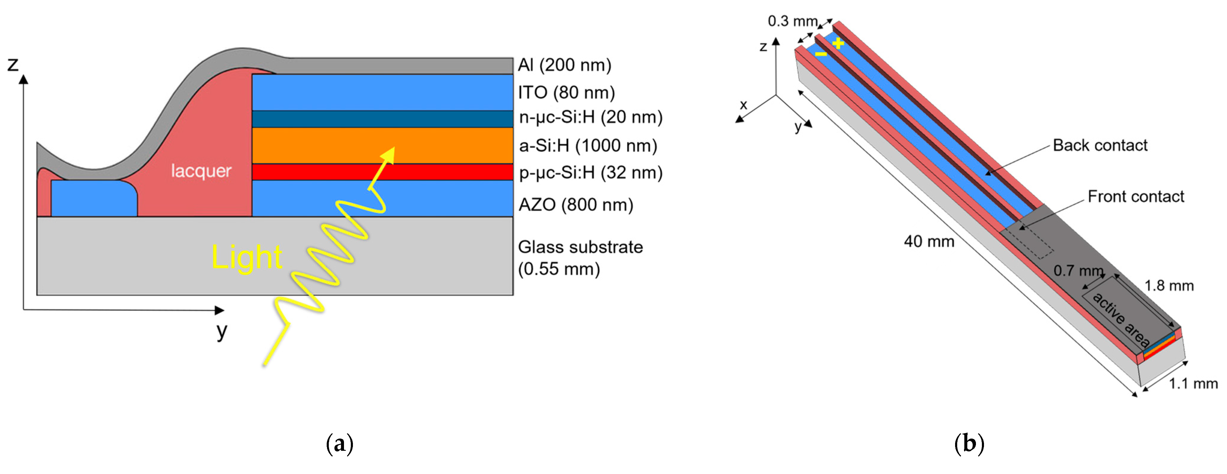
3.1. Sample Preparation
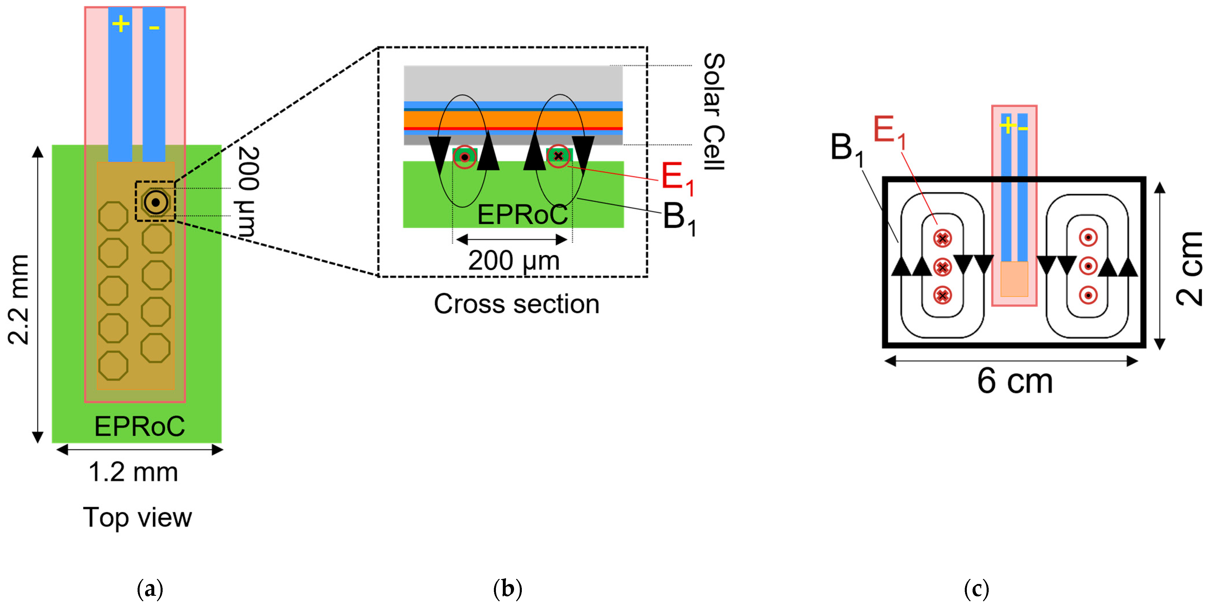
In order to place the pin solar cell into the standard resonator of an X-band EPR spectrometer (Bruker Biospin, Germany), a special cell design is needed. In Figure 3a, the layer structure of the a-Si:H pin solar cell [8,47] used for the EDMR experiments is shown. The operating principles of a-Si:H pin solar cells may be found in detail in [48]. The fabrication process was performed in multiple steps and the layers were deposited sequentially on top of each other. The aluminum-doped zinc-oxide (AZO) layer was deposited via magnetron sputtering onto the glass substrate (100 cm2, 0.55 mm thick). The a-Si:H absorber, as well as the two µc-Si:H electrical contacts were deposited via radio-frequency plasma-enhanced chemical vapor deposition (RF-PECVD). The indium tin-oxide (ITO) layer was also deposited via magnetron sputtering. The structuring of each layer of the solar cell was then performed by the means of three consecutive photolithography and etching steps after applying a photoresistive mask. The metallization comprised the final step of the fabrication process. A layer of aluminum was deposited via thermal evaporation onto the ITO contact that serves as both a back mirror and the low resistivity layer which reduces the series resistance losses. Finally, the as-fabricated device was cut with a dicing saw (DISCO DAD3220, Japan) into small sections (40 mm by 1.1 mm) to permit their placement into the EPR resonator. The photolithographic fabrication method was preferred among other fabrication processes, such as laser scribing used to produce similar samples [9], as it produced less defects at the edge of the samples. The absorber is a 1 µm intrinsic a-Si:H layer. The optimal thickness of the intrinsic absorber in a-Si:H pin solar cells is around 150–300 nm [49], but a larger i-layer width increases the EDMR signal intensity, resulting in a greater SNR of the EDMR signal to allow for a better evaluation of the EDMRoC for PV research. The pin solar cell was deposited with an as large as possible intrinsic layer thickness, so that for a large forward bias ( V b i a s > V c ) the maximum intensity of the EDMR signal can be obtained. In this way, the sample may be considered as a bulk a-Si:H sample with optimal “ohmic type” contacts that allows for very high current densities and stable contact configurations. The 20 nm n-doped µc-Si:H and 32 nm p-doped µc-Si:H layers form the electrical contacts which ensure charge carrier separation and thereby allow for current extraction. The µc-Si:H was used as the electrical contacts since the EDMR signals resulting from µc-Si:H can easily be differentiated from those resulting from a-Si:H, and can subsequently be easily removed from the spectrum at a low T. At RT, the µc-Si:H layer does not show a signal [46]. This decision was made based on results reported in [11,46], where a minimal influence on the recorded EDMR signal at room temperature was observed, confirming that the EDMR signal originated from the absorber. Special concerns were dedicated to the design of the metal contacts to minimize the distortion of the microwave radiation inside the resonator induced by the metal. When the thickness of the contact layers is comparable to the skin depth of the microwaves (~1 µm for Al at ~9 GHz), the presence of metal can lead to B1 field inhomogeneity and attenuation due to dielectric loss [50]. The front contact is composed of an 800 nm thick layer of transparent (in the visible part of the solar spectrum) and electrically conductive AZO (~14 µm for Al at ~9 GHz), while the back contact is composed of a 200 nm light-reflective aluminum deposited onto a layer of 80 nm of ITO. The active area of the solar cell is 1.26 mm2 (1.8 mm × 0.7 mm). These layers were deposited onto a 0.55 mm thick glass substrate and the contacts were formulated into long pads (Figure 3b) to permit electrical connections of the solar cell to monitor the current for EDMR detection [46].

3.2. EDMR-on-a-Chip

The EDMRoC is a combination of an injection-locked VCO-array EPRoC, which is used to generate the B1 field [51], and a transimpedance amplifier on a chip, which is used to monitor the EDMR signal [52]. Photographs of the EDMRoC, VCO array, and TIA are shown in Figure 4a–c. The printed circuit board (PCB) was designed to be compact in size (11 cm × 6 cm) for use with equally compact permanent magnets in the future. For proof of principle, a conventional Bruker B-E 25 electromagnet was used. The EPRoC, consisting of 12 phase-synchronized VCOs and a chain of frequency dividers to readout the VCO frequency (Figure 3b), was bonded directly onto the top of the PCB and a reference frequency was supplied to the chip using an adjustable microwave signal generator (Rohde & Schwarz SMB100B, Germany). The VCO array was designed to oscillate at 13.44 GHz. The B1 field was generated by the 12-VCO array with the magnetic field being perpendicular to the chip’s surface. The voltage was supplied to the PCB using a programmable voltage source (Keithley 230, USA). The intensity of B1 was varied by changing the current, IVCO, in the coils using the potentiometer placed on the PCB. The design of the a-Si:H pin solar cell used to perform the experiments is shown in Figure 2. The cell was placed with the top Al contact facing the VCO array. The front and back electrical contacts of the solar cell shown in Figure 3b were extended to the outside of the solar cell through the AZO layer and were connected to the metal traces of the transimpedance amplifier (TIA, Figure 4a) using silver paste. A bias voltage, Vbias, was applied across the solar cell using a variable power supply (RND 320-KA3305P, Switzerland). The dynamic range of the detectable DC current in the solar cell was varied by selecting different resistance values (20 kΩ, 100 kΩ, and 1 MΩ, respectively) and was monitored using a digital multimeter (SMI970 QUAD DVM). The EDMR signal was then detected by measuring the AC current output of the TIA using a lock-in amplifier (Anfatec eLockIn 203, Germany) and a 10 kHz modulation. The transimpedance amplifier is typically used to convert and amplify the input current (Iin) to an output voltage (Vout) proportional to the resistance of the circuit via a feedback resistor Rf using an operational amplifier with a sufficiently high input impedance to dictate the current flow through the Rf. Therefore, changing the value of the resistance via Rf increases Vout such that Rf = Vout/Iin, where Rf in the onboard TIA was 1.2 MΩ. The design and electrical properties of the onboard TIA used in this work may be found in [52]. In Figure 4d, a block diagram of the EDMRoC spectrometer is shown. Figure 5a–c show a schematic of the a-Si:H pin solar cell placed both on top of the EPRoC and inside the resonator. The rectangular boxes represent the glass substrate covered by a thin lacquer (shown in red), where the active area of the solar cell (shown in orange) covers the entire array’s surface. The twelve octagons represent the coils of the chip where the B1 field is generated perpendicular to each coil. In Figure 5b, a side view of the solar cell placed on top of the chip depicts the interaction of the B1 field with the PV-active area of the solar cell, thereby alleviating the geometrical constraints imposed using a conventional spectrometer for EDMR measurements, as outlined previously. In principle, any solar cell of an arbitrary shape may be placed on top of the EDMRoC VCO array to perform EDMR measurements, provided that the chip–PCB surface is sufficiently flat. This can be accomplished using through-silicon VIAS, which would permit the removal of the bonding wires from the chip and will be the focus of the next generation EDMRoC devices.
In Figure 5c, a schematic of the solar cell placed in a conventional EPR resonator is shown. The microwave radiation generated by the microwave bridge of the EPR spectrometer is coupled to the resonator. In this implementation, the B1 field excites the entire active area of the solar cell homogeneously. Resonators designed to perform continuous wave EPR are typically constructed to maximize the Q-factor while providing spatial separation between the microwave magnetic field B1 and the microwave electric field E1. However, the sample may extend into the electric field if it is not properly placed inside the cavity, decreasing the Q-factor and inducing heating effects as a result. In the case of the EDMR samples, the metal contacts that are used to extract the EDMR signal may act as microstrip-like resonators, thereby increasing the field strength in the sample [53]. This can, in some cases, enhance the current in the sample, resulting in a reduced signal-to-noise ratio of the EDMR spectrum [10]. A thorough description of the conventional EDMR experimental configuration may be found in [37]. One of the advantages of the EDMRoC is that the electric field does not interfere with the sample [54]. Due to the characteristic power saturation behavior of the EDMR signal, the EDMRoC can be designed to produce high intensities of B1 from 380 µT and beyond to further increase the signal amplitude even at very high microwave frequencies (e.g., >100 GHz) [16,55]. The Bruker Elexsys E780 263 GHz EPR spectrometer has a very limited sample space (~0.2 mm inner diameter sample tubes) when using the TE011 resonator, and is too small for pin solar cells [56]. Thus, EDMR experiments at high frequencies are typically performed using a non-resonant probehead, which has similar size constraints of an EPR resonator, but suffers from a greatly reduced Q-factor. Moreover, for pulse EDMR experiments, the Bruker 263 GHz system is limited by the maximum B1 amplitude of 10 µT, which corresponds to a π-pulse length of ~2 µs, and represents a limitation for pulsed-EDMR experiments on samples with short relaxation times, especially when considering electron-spin echo-envelope modulation (ESEEM) experiments, for which the nuclear Larmor frequency for 29Si ≈ 80 MHz at 9.4 T [7]. The high intensity B1 possible with the VCO array design is especially advantageous for EDMR experiments at higher frequencies. Previous results using EPRoC technologies [16] show the possibility to generate 40 µT B1 fields at 140 GHz. Further developments will allow electrically detected Rabi nutation experiments [17] at higher frequencies using an EDMRoC at 263 GHz [19].

3.3. EDMRoC Measurements
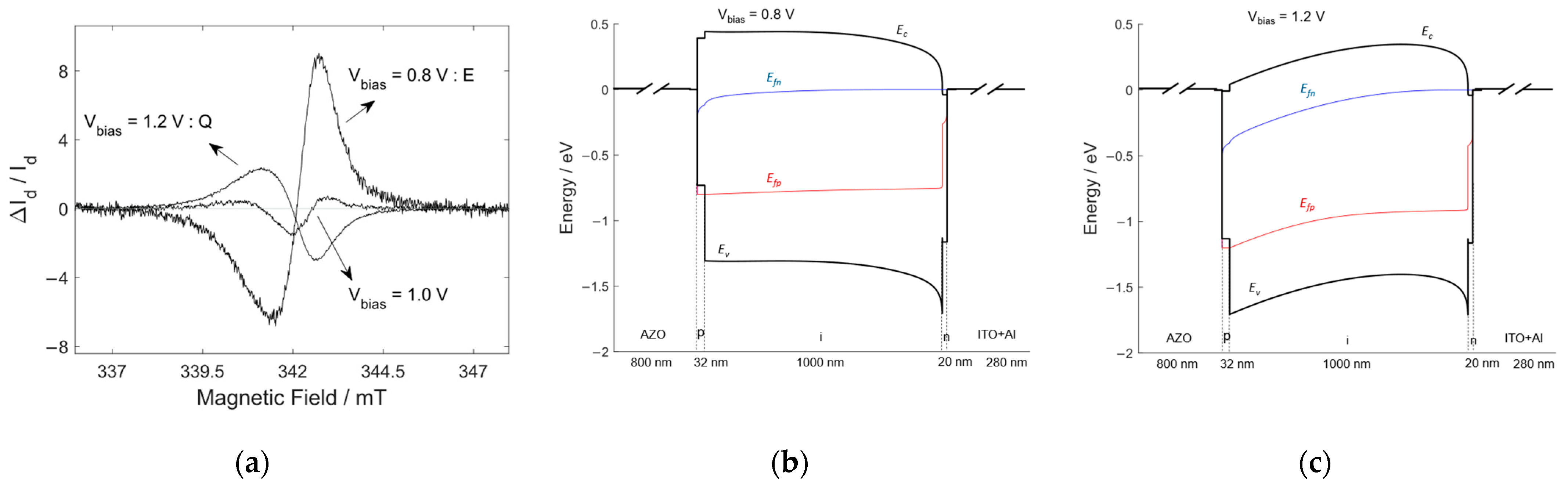
To perform EDMRoC measurements, the solar cell was interfaced to the TIA by adhering the electrical contacts to the metal traces of the PCB using a thin layer of silver paste (G 302 PLANO GmbH, Germany). The back contact of the solar cell was placed directly onto the VCO array in such a way that it covered all 12 coils of the array while minimizing the distance between the array and the solar cell. The surface of the array is electrically isolated against the back contact of the cell. As the spin-flip induced current change is detected instead of the relaxation-determined EPR signal during the experiment, saturation due to excess microwave B1 is typically not observed, such that the maximum obtainable B1 may be used during EDMRoC measurements. The VCO array was designed to oscillate at a constant frequency (13.44 GHz) while varying the magnetic field; therefore, the EDMRoC experiments presented herein were performed by the means of continuous wave (CW) experiments, sweeping the magnetic field from 490 mT to 505 mT in 0.1 mT steps, respectively, while recording the signal intensity at each step. To reduce the 1/f noise and to maximize the resulting EDMR signal, a modulation frequency of 10 kHz was used in the experiments reported [57]. A frequency deviation, f d e v , of 9.0 MHz was used, which allowed for the integration of the detected signal over a bandwidth that was equivalent to a ~0.3 mT magnetic field modulation in a typical EPR experiment. The signal was recorded using a lock-in amplifier (Anfatec eLockIn 203, Germany) and a time constant τ = 50 ms. For each presented spectrum, a total of 10,000 field sweeps were recorded. The acquisition time for each scan was around 7.5 s. The EDMR signal was acquired for different forward Vbias in dark conditions. The current–voltage (I–V) response curve of the solar cell was recorded under dark conditions measuring the DC current output using a digital multimeter (SMI970 QUAD DVM), which was then used to determine the approximate conditions under which the solar cell was operating during the EDMR measurements.
EDMRoC principally allows for frequency sweeps instead of magnetic field sweeps, which enables the use of a permanent magnet during the experiment. The herein reported chip has this capability; however, due to excessive phase noise an EDMR signal with a sufficiently high SNR was not observed. In the next generation EDMRoC, this feature will be further explored. EDMR measurements were also performed using a commercial Bruker Elexsys E580 X-band EPR spectrometer for comparison. The solar cell was connected to an external TIA (Elektronik-Manufaktur Mahlsdorf, Germany) and was inserted inside a dielectric resonator (Bruker ER4118X-MD5-W1, Germany). Spectra were recorded using a 10 kHz modulation frequency, a 0.3 mT magnetic field modulation, a 20.48 ms lock-in amplifier time constant, and a 40.96 ms conversion time. The presented spectra were recorded using 10 field sweeps and 150 kΩ Rf in the external TIA. The results of the measurements performed using the conventional spectrometer were used as a reference for comparison with the results obtained using the EDMRoC. The B1 field intensity inside the resonator was around 20 µT, and was similar to the intensity of the B1 field generated about the EPRoC surface [15]. The spectral simulations and least-squares fitting of the data were performed using the pepper function for simulating powder-averaged spectra and the esfit function, respectively, provided by the EasySpin library [58].

4. Results

The I–V curve of the solar cell was recorded while varying the Vbias in dark conditions with the microwaves on and off (Figure 6). It may be observed that the dark current increases when the microwaves are switched on when using the EDMRoC device, while when measuring with the conventional spectrometer the I–V curves were observed to be independent of both the microwaves and the external magnetic field. This effect may be either attributed to (i) an increase in the solar cell temperature due to resistive heating induced by the high current present in the EDMRoC coils, or (ii) to an unknown electric field effect due to the presence of the E-field that typically occurs in conventional EDMR experiments in a resonator. Case (i) is more likely, because in the absence of an active cooling system, the heat produced at high-bias currents in the coil is not properly dissipated, and consequently, the solar cell is heated via radiative heating by the VCO array during the EDMR measurements. This effect can be easily modelled since the temperature dependence of the I–V curve has been well established. The I–V curve in the dark state corresponds to a diode, and it may be modelled as follows [48,59]:
J = J 0 e q n   k b   T   V b i a s   R s   J 1
where J0 is the dark saturation current, q is the elementary charge, kb is the Boltzmann constant, n is the diode ideality factor, T is the temperature, and Rs is the series resistance, which is primarily influenced by the metal contacts of the cell. The ideality factor reflects the recombination-determined behavior of the solar cell with respect to an ideal diode.
The previously described relationship (Equation (4)) was rearranged to express Vbias as a function of the current density, J, in order to perform a fit to the experimental data:
V b i a s = 1 α log J J 0 1 + R s   J  
where α = q n   k b   T . In this form, the values of n, T, J0, and Rs can be directly determined. To ensure the best global fit, the linear terms (α and Rs) and the non-linear term (J0) of Equation (5) were fit separately using a non-linear least-squares algorithm (lsqnonlin, MATLAB, Mathworks, USA). To prevent the over parametrization of the fitting routine, the data were first fit via the I–V curve recorded without the bias current applied to the VCO array such that the microwaves, and therefore the B1 field, were not present. In this way, the temperature parameter was kept constant at T = 25 °C, and the ideality factor n = 2.12 was determined empirically. The I–V curve was then recorded during the EDMR measurements with microwaves present at the maximum B1 obtainable and was subsequently fit using the routine established in the absence of microwaves (see Figure 6), such that the values of the dark saturation current J0, the series resistance Rs, and the temperature T were estimated while keeping n constant at the previously estimated value. The results of this analysis were as follows: Rs = 8 Ω cm2, J0= 8 × 10⁻⁹ mA/cm2, and T = 63 °C. The good agreement with the experimental data suggests that the excess heating due to the lack of an active cooling system was the most likely cause of the microwave-induced change observed in the I–V curve.
In Figure 7, the results of the EDMR measurements for Vbias = 1.2 V are shown. In Figure 7a, the black curve represents the experimental result measured using the resonator-based conventional X-band EPR spectrometer. It has been previously reported in the literature that for values of Vbias large enough to reverse the direction of the electric field present in the intrinsic layer, the EDMR signal results from quenching processes [43], as explained above. The line-shape of the recorded spectrum exhibits an asymmetry in the low-field region due to the presence of contributions from both the dangling bond (averaged gdb = 2.0055) and the valence band tail (VBT) (gVBT = 2.01) signals, as previously reported [3]. A thorough analysis of the nature of the dangling bond in amorphous silicon has been performed via multifrequency EPR, and is reported in [60]. As shown in [23], the EDMR signal from these db states can be well fitted using a rhombic g tensor (with gdb = [2.0079 2.0061 2.0034]) and disorder-induced terms (the so called g-strain), gdb-strain = [0.0054 0.0022 0.0018])). Note that it is at present not clear for why the CBT-db spin pair has a g tensor which resembles that of a dangling bond.
The interaction with the low concentration of 29Si results in an axially symmetric hyperfine tensor values, A = [151 151 269], in MHz. The VBT are considered with the addition of an isotropic line with gVBT and ΔHpp,VBT. The intensities of these two components, the linewidth (ΔHpp), the gVBT, and the weight (w) of the dangling bonds and VBT contributions were obtained by fitting. The results were as follows: gVBT = 2.0089(1), ΔHpp,db = 1.21(4) mT, ΔHpp,VBT = 0.913(3) mT, wVBT = 0.6(1), and wdb = 0.4(1). These results are in agreement with previous analyses performed on similar samples, although the weight of the VBT contribution is a factor of three greater than what has been reported in the literature [11]. This discrepancy can be attributed to differences in the thickness of the intrinsic layer of the sample reported herein, which was around three times larger than the samples reported previously [11,41], and hence the overall contribution from the trapping processes close to the p–i interface may be more dominant compared to other cases [44].
Figure 7b shows the EDMR measurement performed using the EDMRoC with the TIA on a chip. For these data, a simulation was performed using the same fitting parameters as obtained from the data in Figure 7a and was then linearly scaled to the experimentally obtained signal intensities. After consideration of the differences in the SNR, the line-shapes from both measurements were found to be in agreement.

5. Discussion

From Figure 7, it could be perceived that the EDMRoC is well suited for structure-determining the EDMR experiments in solar cells; however, the SNR was significantly reduced in the EDMRoC-obtained data by over an order of magnitude compared to the conventional EDMR. For the comparison between these two measurements, two parameters were considered; the integrated current change over the magnetic field, Δ I d , normalized to the overall current, Id, and the SNR. The variation of the current, ΔId, due to the microwave radiation was calculated according to the following formula:
Δ I d = I d · V o u t R f
where Id is the DC dark current of the solar cell, Vout is the voltage output from the lock-in amplifier, and Rf is the resistance that defines the amplification factor of the TIA. The ratio between the obtained value Δ I d   I d E l e x s y s and Δ I d   I d E D M R o C is approximately 30. This difference may be attributed to two factors; the decreased active area of the solar cell that is accessible by the B1 field of the EDMRoC, and the increased temperature of the solar cell due to radiative heating from the VCO array during the EDMRoC experiments. As shown in Figure 5, the B1 field generated by the VCO array in the EDMRoC does not excite the entire active area of the solar cell; however, in the commercial EPR resonator, the B1 field penetrates the entire area (1.26 mm2) of the solar cell, such that the ratio of active areas ( A E D M R o C / A E l e x s y s   0.3 ) results in a decrease in the EDMRoC signal intensity by approximately the same ratio. As the current in the device generates additional noise, it is increasingly important that the B1 field penetrates the entire device, such that the EDMR signal intensity is greater than the integrated current noise in the device. Moreover, insufficient heat dissipation in the EDMRoC at higher temperatures (TC ≈ 63 °C = 336 K) compared to the conventional spectrometer (TE ≈ 29 °C = 302 K) further reduces the signal intensity observed due to the increased probability that the electron trapped in the vicinity of the midgap dangling bond is reemitted to the conduction band [61]. Enhancements in the spin pair dissociation rate, d, results in a decrease in the EDMR signal intensity as ΔI/I∝1/d [62]. Hence, at higher temperatures, ΔI/I decreases proportionally to the Boltzmann factor e Δ E k b T , where ΔE is the activation energy for the thermal emission of the CBT electron to the conduction band (see Figure 1a,b). It has been assumed that the trapped state of the CBT electron is within a single energy level in the bandgap of a-Si-H. To determine ΔE empirically, temperature-dependent EDMR measurements were performed using the conventional spectrometer and a cavity resonator which was designed for experiments at elevated temperatures (Bruker ER4114HT and BVT3000 controller/BVTB3500 heater) and are shown in Figure 8.
Considering both the reduced accessible area and the increased temperature of the solar cell, the expected EDMRoC signal Δ I / I E M D R o C * may be estimated as:
Δ I I * E D M R o C = Δ I I E l e x s y s · 1 Δ r   · A E D M R o C A E l e x s y s
where the temperature of the solar cell with (Ton) and without (Toff) microwaves results in a decrease in the signal intensity according to Δ r e Δ E k b 1 T o f f 1 T o n .
As Δ r is determined by the activation energy, Δ E , the dependence of the EDMR signal on temperature was measured between room temperature and 335 K (Figure 8) to determine the activation energy of the spin-dependent recombination processes according to the Arrhenius formula:
ln Δ I I = ln A + Δ E k b T  
where ΔE is the activation energy of the spin pair CBT electron emission into the conduction band, ln(A) is the natural logarithm of the pre-exponential factor of the Arrhenius relation, kb is the Boltzmann constant, and T is the temperature. After performing a linear fit to the logarithmically expressed experimental data, the activation energy, Δ E 0.4 ± 0.1   eV , and the natural logarithm of the pre-exponential factor, ln(A) = −15.4 ± 0.5, were obtained. The activation energy of about 0.4–0.5 eV was expected for deep trapping at a defect in the conduction band tail. With Δ E = 0.4   eV , a value of Δ r = 4.7 was obtained, which is in agreement with what has been obtained experimentally ( Δ r = 7 ).
The SNR was calculated as the peak-to-peak intensity of the recorded signal divided by the standard deviation of the noise and was normalized to the square root of the number of recorded field sweeps, resulting in an observed SNR ratio S N R E l e x s y s S N R E D M R o C 340 . As the ΔId/Id obtained with the EDMRoC is a factor of 30 less than that obtained using the Elexsys spectrometer, the noise in the EDMRoC measurements was therefore approximately a factor of 10 greater than that obtained using the Elexsys spectrometer. This increase may be attributed to the additional shot noise present in the solar cell when it was placed on the EDMRoC, and was further supported by the decrease in the SNR observed in the conventional resonator ( S N R T = 302   K S N R T = 336   K 12 ) with respect to the increased temperature [52,63]. It was observed when performing the EDMRoC measurements using an EPRoC with thermal dissipation via direct contact with the copper substrate contained within the PCB and an external homebuilt TIA that the SNR was increased by a factor of two, demonstrating the potential improvements to the noise floor by decreasing the temperature of the VCO array (data not shown). As the EDMRoC and the TIA on the chip are confined to a single PCB, the increased noise may be reduced by placing the EDMRoC and the TIA on the chip in a cryostat to perform measurements where the sample and the device are both cooled to cryogenic temperatures [64].
In summary, we were able to demonstrate that the EDMRoC can detect the EDMR signal associated with recombination through bulk dangling-bond defects in the intrinsic absorber layer of a-Si:H pin solar cells. The discrepancy between the SNR obtained with the EDMRoC and the resonator-based conventional spectrometer may be ascribed to the smaller excitation volume of the EDMRoC and the elevated temperature of the solar cell due to the lack of an adequate thermal dissipation in the VCO array of the EDMRoC sensor. In the next generation of the EDMRoC spectrometer, larger VCO arrays and thermal dissipation via active cooling circuits, as well as improvements to the thermal stability and the noise floor, combined with additional and variable Rf values in the onboard TIA will result in a more versatile device with a greater performance with respect to the SNR and a significantly improved applicability for thin-film photovoltaic investigations [65].

6. Conclusions and Outlook

We have successfully demonstrated a proof of concept for applying an EDMRoC to characterize thin-film solar cells. It was shown that the combination of a VCO array and an onboard TIA may be used to perform I–V and EDMR measurements. As the EDMRoC is a single-board system, the noise in the TIA will be greatly reduced when cryogenically cooling the sample, thereby enhancing the overall SNR of the EDMRoC signal. The herein reported prototype EDMRoC does not fit into a standard cryostat; however, this will be the subject of future investigations, as the device progresses beyond the current form factor limitations. Furthermore, the EDMRoC potentially also allows for EDMR experiments using frequency sweeps instead of field sweeps and in combination with a permanent magnet, will yield a compact and portable EDMRoC spectrometer [15,66]. Increasing both the size and the number of coils in the VCO array will allow for conducting investigations in samples with arbitrary geometries of increasingly larger volumes where the signal intensity is expected to increase linearly with increases in the active volume of the B1 field, as long as the large filling factor of the EDMRoC is preserved. This is especially beneficial for small samples, such as thin films and nanodevices, as the VCO array may be tailored to the device under investigation such that the filling factor is maximized with respect to the device. The EDMRoC represents an innovative and promising spectrometer that is both inexpensive and very versatile in performing in situ and operando analyses on thin-film materials and devices. However, heat dissipation and increased phase stability when performing frequency sweeps will be necessary to realize these applications.
Though the experiments demonstrated in this report were all recorded via CW microwave irradiation, it has been previously demonstrated that the underlying dynamics that contribute to the fundamental radical pair mechanisms present in both silicon solar cells and organic solar cells are better investigated by pulsed microwave EDMR techniques [37,67]. Recently, an EPR-on-a-chip device operating at 30.4 GHz successfully demonstrated pulsed EPR measurements through recording the resulting Rabi oscillations following microwave excitation [17]. This is extremely enticing for the future generation of EDMRoC spectrometers and would greatly increase the utility of the device for detecting the different contributions to radical pairing, while also likely improving the SNR of the spectrometer overall. More recently, an EPRoC sensor capable of operating at 263 GHz has been presented to enable the access to pulsed EDMRoC experiments at higher frequencies, where B0 fields are in the range of 9.4 T [19]. Additionally, EPRoC technologies are currently being developed to access frequencies as high as 780 GHz within the framework of the DFG priority program INTEREST. The EDMRoC is at the threshold of becoming a mature spectroscopy such that EDMR investigations may be accessed at very low investment costs, provided that the above-mentioned restrictions can be solved in the near future.

Author Contributions

M.S., J.E.M., B.N., J.A. and K.L. defined the goals of the research and designed the experiments. M.S. performed all the EDMRoC experiments. M.S., G.M. and J.E.M. performed EDMR experiments on the conventional spectrometer. M.S. and G.M. performed the EDMR simulations. D.D. designed the TIA and the PCB. A.C. designed the 12-coils array EPRoC. D.A. designed the masks for the solar cell processing and deposited the Al layer on the glass substrate. S.N. and B.S. performed the deposition processes of a-Si:H. K.J. and I.R. performed the etching and the photolithography processes. C.T.T. simulated the band diagram of the solar cell. M.S., J.E.M., G.M., B.N. and K.L. evaluated the results of the experiments and wrote the manuscript. All authors have read and agreed to the published version of the manuscript.

Funding

This work has been supported by the Bundesministerium für Bildung und Forschung under contract number 01186916/1 (EPRoC), by the HEMF (Helmholtz Energy Materials Foundry) infrastructure funded by the Helmholtz association (HGF), and by the DFG priority program INtegrated TERahErtz sySTems Enabling Novel Functionality (INTEREST) (SPP 2314). B.N. acknowledges the financial support from the Deutsche Forschungsgemeinschaft (project numbers 410866378 and 410866565).

Data Availability Statement

Data will be made available upon reasonable request.

Acknowledgments

We are grateful to Jannik Möser, Carlos Graeff, Michal Kern, Silvio Künstner, and Jan Behrends for experimental support and for helpful discussions.

Conflicts of Interest

The authors declare no conflict of interest.

References

  1. Silva, G.B.; Santos, L.F.; Faria, R.M.; Graeff, C.F.O. EDMR of MEH-PPV LEDs. Phys. B Condens. Matter 2001, 308–310, 1078–1080. [Google Scholar] [CrossRef]
  2. Behrends, J.; Schnegg, A.; Lips, K.; Thomsen, E.A.; Pandey, A.K.; Samuel, I.D.W.; Keeble, D.J. Bipolaron Formation in Organic Solar Cells Observed by Pulsed Electrically Detected Magnetic Resonance. Phys. Rev. Lett. 2010, 105, 176601. [Google Scholar] [CrossRef] [Green Version]
  3. Lips, K.; Fuhs, W. Transport and Recombination in Amorphous p-i-n-type Solar Cells Studied by Electrically Detected Magnetic Resonance. J. Appl. Phys. 1993, 74, 3993–3999. [Google Scholar] [CrossRef]
  4. Boehme, C.; Lips, K. Theory of Time-Domain Measurement of Spin-Dependent Recombination with Pulsed Electrically Detected Magnetic Resonance. Phys. Rev. B 2003, 68, 245105. [Google Scholar] [CrossRef]
  5. Morishita, H.; Vlasenko, L.S.; Tanaka, H.; Semba, K.; Sawano, K.; Shiraki, Y.; Eto, M.; Itoh, K.M. Electrical Detection and Magnetic-Field Control of Spin States in Phosphorus-Doped Silicon. Phys. Rev. B 2009, 80, 205206. [Google Scholar] [CrossRef] [Green Version]
  6. McCamey, D.R.; Huebl, H.; Brandt, M.S.; Hutchison, W.D.; McCallum, J.C.; Clark, R.G.; Hamilton, A.R. Electrically Detected Magnetic Resonance in Ion-Implanted Si:P Nanostructures. Appl. Phys. Lett. 2006, 89, 182115. [Google Scholar] [CrossRef] [Green Version]
  7. Akhtar, W.; Schnegg, A.; Veber, S.; Meier, C.; Fehr, M.; Lips, K. CW and Pulsed Electrically Detected Magnetic Resonance Spectroscopy at 263GHz/12T on Operating Amorphous Silicon Solar Cells. J. Magn. Reson. 2015, 257, 94–101. [Google Scholar] [CrossRef] [PubMed] [Green Version]
  8. Xiao, L.; Astakhov, O.; Finger, F. Silicon Thin Film Powder Samples for Electron Spin Resonance Investigation: Role of Substrate and Preparation Procedure. Jpn. J. Appl. Phys. 2011, 50, 071301. [Google Scholar] [CrossRef]
  9. Haas, S.; Gordijn, A.; Stiebig, H. High Speed Laser Processing for Monolithical Series Connection of Silicon Thin-Film Modules. Prog. Photovolt. Res. Appl. 2008, 16, 195–203. [Google Scholar] [CrossRef]
  10. Lo, C.C.; Bradbury, F.R.; Tyryshkin, A.M.; Weis, C.D.; Bokor, J.; Schenkel, T.; Lyon, S.A. Suppression of Microwave Rectification Effects in Electrically Detected Magnetic Resonance Measurements. Appl. Phys. Lett. 2012, 100, 063510. [Google Scholar] [CrossRef]
  11. Möser, J. Charge Transport in Amorphous Silicon: A Study by Electrically Detected Magnetic Resonance; Freie Universität: Berlin, Germany, 2019. [Google Scholar]
  12. Klotz, F.; Huebl, H.; Heiss, D.; Klein, K.; Finley, J.J.; Brandt, M.S. Coplanar Stripline Antenna Design for Optically Detected Magnetic Resonance on Semiconductor Quantum Dots. Rev. Sci. Instrum. 2011, 82, 074707. [Google Scholar] [CrossRef] [Green Version]
  13. McCrory, D.J.; Anders, M.A.; Ryan, J.T.; Shrestha, P.R.; Cheung, K.P.; Lenahan, P.M.; Campbell, J.P. Slow- and Rapid-Scan Frequency-Swept Electrically Detected Magnetic Resonance of MOSFETs with a Non-Resonant Microwave Probe within a Semiconductor Wafer-Probing Station. Rev. Sci. Instrum. 2019, 90, 014708. [Google Scholar] [CrossRef] [PubMed]
  14. Chu, A.; Schlecker, B.; Kern, M.; Goodsell, J.L.; Angerhofer, A.; Lips, K.; Anders, J. On the Modeling of Amplitude-Sensitive ESR Detection Using VCO-Based ESR-on-a-Chip Detectors; EPR/Instrumentation: Urbana, IL, USA, 2021. [Google Scholar]
  15. Künstner, S.; Chu, A.; Dinse, K.-P.; Schnegg, A.; McPeak, J.E.; Naydenov, B.; Anders, J.; Lips, K. Rapid-Scan Electron Paramagnetic Resonance Using an EPR-on-a-Chip Sensor. Magn. Reson. 2021, 2, 673–687. [Google Scholar] [CrossRef]
  16. Matheoud, A.V.; Gualco, G.; Jeong, M.; Zivkovic, I.; Brugger, J.; Rønnow, H.M.; Anders, J.; Boero, G. Single-Chip Electron Spin Resonance Detectors Operating at 50GHz, 92GHz, and 146GHz. J. Magn. Reson. 2017, 278, 113–121. [Google Scholar] [CrossRef] [Green Version]
  17. Hassan, M.A.; Kern, M.; Chu, A.; Kalra, G.; Shabratova, E.; Tsarapkin, A.; MacKinnon, N.; Lips, K.; Teutloff, C.; Bittl, R.; et al. Towards Single-Cell Pulsed EPR Using VCO-Based EPR-on-a-Chip Detectors. Frequenz 2022, 76, 699–717. [Google Scholar] [CrossRef]
  18. Böhme, C. Dynamics of Spin-Dependent Charge Carrier Recombination; Cuvillier Verlag: Göttingen, Germany, 2003. [Google Scholar]
  19. Chu, A.; Kern, M.; Khan, K.; LiPS, K.; Anders, J. A 263GHz 32-Channel EPR-on-a-Chip Injection-Locked VCO-Array. In Proceedings of the 2023 IEEE International Solid—State Circuits Conference (ISSCC), San Francisco, CA, USA, 19–23 February 2023; pp. 20–22. [Google Scholar]
  20. Cochrane, C.J.; Lenahan, P.M.; Lelis, A.J. An Electrically Detected Magnetic Resonance Study of Performance Limiting Defects in SiC Metal Oxide Semiconductor Field Effect Transistors. J. Appl. Phys. 2011, 109, 014506. [Google Scholar] [CrossRef]
  21. Graeff, C.F.O.; Brandt, M.S.; Stutzmann, M.; Powell, M.J. Defect Creation in Amorphous-Silicon Thin-Film Transistors. Phys. Rev. B 1995, 52, 4680–4683. [Google Scholar] [CrossRef]
  22. George, B.M.; Behrends, J.; Schnegg, A.; Schulze, T.F.; Fehr, M.; Korte, L.; Rech, B.; Lips, K.; Rohrmüller, M.; Rauls, E.; et al. Atomic Structure of Interface States in Silicon Heterojunction Solar Cells. Phys. Rev. Lett. 2013, 110, 136803. [Google Scholar] [CrossRef]
  23. Boehme, C.; Behrends, J.; Maydell, K.v.; Schmidt, M.; Lips, K. Investigation of Hopping Transport in N-a-Si:H/c-Si Solar Cells with Pulsed Electrically Detected Magnetic Resonance. J. Non-Cryst. Solids 2006, 352, 1113–1116. [Google Scholar] [CrossRef] [Green Version]
  24. Thoan, N.H.; Jivanescu, M.; O’Sullivan, B.J.; Pantisano, L.; Gordon, I.; Afanas’ev, V.V.; Stesmans, A. Correlation between Interface Traps and Paramagnetic Defects in C-Si/a-Si:H Heterojunctions. Appl. Phys. Lett. 2012, 100, 142101. [Google Scholar] [CrossRef]
  25. Stutzmann, M.; Brandt, M.S.; Bayerl, M.W. Spin-Dependent Processes in Amorphous and Microcrystalline Silicon: A Survey. J. Non-Cryst. Solids 2000, 266–269, 1–22. [Google Scholar] [CrossRef]
  26. Meyer, A.R.; Taylor, P.C.; Venuti, M.B.; Eley, S.; LaSalvia, V.; Nemeth, W.; Page, M.R.; Young, D.L.; Stradins, P.; Agarwal, S. Atomic Structure of Light-Induced Efficiency-Degrading Defects in Boron-Doped Czochralski Silicon Solar Cells. Energy Environ. Sci. 2021, 14, 5416–5422. [Google Scholar] [CrossRef]
  27. Fehr, M.; Simon, P.; Sontheimer, T.; Leendertz, C.; Gorka, B.; Schnegg, A.; Rech, B.; Lips, K. Influence of Deep Defects on Device Performance of Thin-Film Polycrystalline Silicon Solar Cells. Appl. Phys. Lett. 2012, 101, 123904. [Google Scholar] [CrossRef] [Green Version]
  28. Würz, R.; Meeder, A.; Fuertes Marrón, D.; Schedel-Niedrig, T.; Knop-Gericke, A.; Lips, K. Native Oxidation of CuGaSe2 Crystals and Thin Films Studied by Electron Paramagnetic Resonance and Photoelectron Spectroscopy. Phys. Rev. B 2004, 70, 205321. [Google Scholar] [CrossRef]
  29. Würz, R.; Meeder, A.; Marrón, D.F.; Schedel-Niedrig, T.; Lips, K. An Electron Paramagnetic Resonance and Photoelectron Spectroscopy Study on the Native Oxidation of CuGaSe2. MRS Online Proc. Libr. (OPL) 2005, 865, 536. [Google Scholar] [CrossRef]
  30. Lukina, E.A.; Uvarov, M.N.; Kulik, L.V. Charge Recombination in P3HT/PC70BM Composite Studied by Light-Induced EPR. J. Phys. Chem. C 2014, 118, 18307–18314. [Google Scholar] [CrossRef]
  31. Dyakonov, V.; Zoriniants, G.; Scharber, M.; Brabec, C.J.; Janssen, R.a.J.; Hummelen, J.C.; Sariciftci, N.S. Studies of Photoinduced Charge Transfer in Conjugated Polymer-Fullerene Composites by Light-Induced ESR. AIP Conf. Proc. 1998, 442, 257–260. [Google Scholar] [CrossRef] [Green Version]
  32. Weil, J.A.; Bolton, J.R. Electron Paramagnetic Resonance: Elementary Theory and Practical Applications, 2nd ed.; Wiley-Interscience: Hoboken, NJ, USA, 2007; ISBN 978-0-471-75496-1. [Google Scholar]
  33. van der Est, A. Continuous-Wave EPR. In eMagRes; John Wiley & Sons, Ltd.: Hoboken, NJ, USA, 2016; pp. 1411–1422. ISBN 978-0-470-03459-0. [Google Scholar]
  34. Baranovski, S. Charge Transport in Disordered Solids with Applications in Electronics; John Wiley & Sons: Hoboken, NJ, USA, 2006; ISBN 978-0-470-09505-8. [Google Scholar]
  35. Agarwal, M.; Pawar, A.; Wadibhasme, N.; Dusane, R. Controlling the C-Si/a-Si:H Interface in Silicon Heterojunction Solar Cells Fabricated by HWCVD. Sol. Energy 2017, 144, 417–423. [Google Scholar] [CrossRef]
  36. Blank, A.; Twig, Y.; Ishay, Y. Recent Trends in High Spin Sensitivity Magnetic Resonance. J. Magn. Reson. 2017, 280, 20–29. [Google Scholar] [CrossRef]
  37. Schnegg, A.; Behrends, J.; Fehr, M.; Lips, K. Pulsed Electrically Detected Magnetic Resonance for Thin Film Silicon and Organic Solar Cells. Phys. Chem. Chem. Phys. 2012, 14, 14418. [Google Scholar] [CrossRef] [PubMed] [Green Version]
  38. Kaplan, D.; Solomon, I.; Mott, N.F. Explanation of the Large Spin-Dependent Recombination Effect in Semiconductors. J. Phyique Lett. 1978, 39, 51–54. [Google Scholar] [CrossRef] [Green Version]
  39. Boehme, C.; Lips, K. The Investigation of Charge Carrier Recombination and Hopping Transport with Pulsed Electrically Detected Magnetic Resonance Techniques. In Charge Transport in Disordered Solids with Applications in Electronics; John Wiley & Sons, Ltd.: Hoboken, NJ, USA, 2006; pp. 179–219. [Google Scholar]
  40. Eickelkamp, T.; Roth, S.; Mehring, M. Electrically Detected Magnetic Resonance in Photoexcited Fullerenes. Mol. Phys. 1998, 95, 967–972. [Google Scholar] [CrossRef]
  41. Lips, K.; Block, M.; Fuhs, W.; Lerner, C. Degradation of A-Si:H p-i-n Solar Cells Studied by Electrically Detected Magnetic Resonance. J. Non-Cryst. Solids 1993, 164–166, 697–700. [Google Scholar] [CrossRef]
  42. Fuhs, W.; Lips, K. Recombination in A-Si:H Films and Pin-Structures Studied by Electrically Detected Magnetic Resonance (EDMR). J. Non-Cryst. Solids 1993, 164–166, 541–546. [Google Scholar] [CrossRef]
  43. Lips, K.; Boehme, C.; Fuhs, W. Recombination in Silicon Thin-Film Solar Cells: A Study of Electrically Detected Magnetic Resonance. IEE Proc. Circuits Devices Syst. 2003, 150, 309. [Google Scholar] [CrossRef]
  44. Lips, K. Spin-Dependent Recombination Effects in a-SI:H Pin Solar Cell Devices: A New Characterization Technique. MRS Online Proc. Libr. 1995, 377, 455–466. [Google Scholar] [CrossRef]
  45. Simon, M.S.; Kwok, K.N. Physics of Semiconductor Devices, 3rd ed.; Wiley: Hoboken, NJ, USA, 2021. [Google Scholar]
  46. Behrends, J.; Schnegg, A.; Fehr, M.; Lambertz, A.; Haas, S.; Finger, F.; Rech, B.; Lips, K. Electrical Detection of Electron Spin Resonance in Microcrystalline Silicon Pin Solar Cells. Philos. Mag. 2009, 89, 2655–2676. [Google Scholar] [CrossRef]
  47. Melskens, J.; Schnegg, A.; Baldansuren, A.; Lips, K.; Plokker, M.P.; Eijt, S.W.H.; Schut, H.; Fischer, M.; Zeman, M.; Smets, A.H.M. Structural and Electrical Properties of Metastable Defects in Hydrogenated Amorphous Silicon. Phys. Rev. B 2015, 91, 245207. [Google Scholar] [CrossRef] [Green Version]
  48. Shah, A. Amorphous Silicon Solar Cells. In Solar Cells and Modules; Shah, A., Ed.; Springer Series in Materials Science; Springer International Publishing: Cham, Switzerland, 2020; pp. 139–161. ISBN 978-3-030-46487-5. [Google Scholar]
  49. Qarony, W.; Hossain, M.I.; Hossain, M.K.; Uddin, M.J.; Haque, A.; Saad, A.R.; Tsang, Y.H. Efficient Amorphous Silicon Solar Cells: Characterization, Optimization, and Optical Loss Analysis. Results Phys. 2017, 7, 4287–4293. [Google Scholar] [CrossRef]
  50. Behrends, J. Spin-Dependent Transport and Recombination in Solar Cells Studied by Pulsed Electrically Detected Magnetic Resonance; Institut für Experimentalphysik der Freien Universität: Berlin, Germany, 2010; volume VIII, p. 181 S. [Google Scholar] [CrossRef]
  51. Chu, A.; Schlecker, B.; Lips, K.; Ortmanns, M.; Anders, J. An 8-Channel 13GHz ESR-on-a-Chip Injection-Locked Vco-Array Achieving 200μM-Concentration Sensitivity. In Proceedings of the 2018 IEEE International Solid—State Circuits Conference—(ISSCC), San Francisco, CA, USA, 11–15 February 2018; pp. 354–356. [Google Scholar]
  52. Djekic, D.; Häberle, M.; Mohamed, A.; Baumgärtner, L.; Anders, J. A 440-KOhm to 150-GOhm Tunable Transimpedance Amplifier Based on Multi-Element Pseudo-Resistors. In Proceedings of the ESSCIRC 2021—IEEE 47th European Solid State Circuits Conference (ESSCIRC), Grenoble, France, 13–22 September 2021; pp. 403–406. [Google Scholar]
  53. Kawachi, G.; Graeff, C.F.O.; Brandt, M.S.; Stutzmann, M. Saturation Measurements of Electrically Detected Magnetic Resonance in Hydrogenated Amorphous Silicon Based Thin-Film Transistors. Jpn. J. Appl. Phys. 1997, 36, 121. [Google Scholar] [CrossRef]
  54. Hoehne, F. Electrical Detection of Hyperfine Interactions in Silicon; Technische Universität: München, Germany, 2012. [Google Scholar]
  55. Anders, J. Fully-Integrated CMOS Probes for Magnetic Resonance Applications; EPFL: Lausanne, Switzerland, 2011. [Google Scholar]
  56. Gromov, I. Novel MM-Wave EPR Spectrometer ELEXSYS 7th Series: Design and Performance; 2015. [Google Scholar] [CrossRef]
  57. Lee, S.-Y.; Paik, S.; McCamey, D.R.; Boehme, C. Modulation Frequency Dependence of Continuous-Wave Optically/Electrically Detected Magnetic Resonance. Phys. Rev. B 2012, 86, 115204. [Google Scholar] [CrossRef] [Green Version]
  58. Stoll, S.; Schweiger, A. EasySpin, a Comprehensive Software Package for Spectral Simulation and Analysis in EPR. J. Magn. Reson. 2006, 178, 42–55. [Google Scholar] [CrossRef]
  59. Kaminski, A.; Marchand, J.J.; Laugier, A. I–V Methods to Extract Junction Parameters with Special Emphasis on Low Series Resistance. Solid-State Electron. 1999, 43, 741–745. [Google Scholar] [CrossRef]
  60. Fehr, M.; Schnegg, A.; Rech, B.; Lips, K.; Astakhov, O.; Finger, F.; Freysoldt, C.; Bittl, R.; Teutloff, C. Dangling Bonds in Amorphous Silicon Investigated by Multifrequency EPR. J. Non-Cryst. Solids 2012, 358, 2067–2070. [Google Scholar] [CrossRef] [Green Version]
  61. Dersch, H.; Schweitzer, L.; Stuke, J. Recombination Processes in a -Si:H: Spin-Dependent Photoconductivity. Phys. Rev. B 1983, 28, 4678–4684. [Google Scholar] [CrossRef]
  62. Lips, K.; Lerner, C.; Fuhs, W. Semiclassical Model of Electrically Detected Magnetic Resonance in Undoped A-Si:H. J. Non-Cryst. Solids 1996, 198–200, 267–270. [Google Scholar] [CrossRef]
  63. Davenport, K.; Trinh, C.T.; Hayward, M.; Lips, K.; Rogachev, A. Relaxation Processes in Silicon Heterojunction Solar Cells Probed via Noise Spectroscopy. Sci. Rep. 2021, 11, 13238. [Google Scholar] [CrossRef]
  64. Artzi, Y.; Twig, Y.; Blank, A. Induction-Detection Electron Spin Resonance with Spin Sensitivity of a Few Tens of Spins. Appl. Phys. Lett. 2015, 106, 084104. [Google Scholar] [CrossRef] [Green Version]
  65. Sherman, A.; Zgadzai, O.; Koren, B.; Peretz, I.; Laster, E.; Blank, A. Diamond-Based Microwave Quantum Amplifier. Sci. Adv. 2022, 8, eade6527. [Google Scholar] [CrossRef]
  66. Anders, J.; Lips, K. MR to Go. J. Magn. Reson. 2019, 306, 118–123. [Google Scholar] [CrossRef]
  67. Boehme, C.; Lips, K. A Pulsed EDMR Study of Hydrogenated Microcrystalline Silicon at Low Temperatures: A Pulsed EDMR Study of Hydrogenated Microcrystalline Silicon. Phys. Status Solidi (C) 2004, 1, 1255–1274. [Google Scholar] [CrossRef]
Figure 1. (a) Spin-dependent recombination processes through defect states in the forward-bias dark current of an a-Si:H pin solar cell, where only the intrinsic (i) layer is shown. The free charge carriers (electrons, blue filled circles, and holes, red filled circles) are injected into the device (1) through the selective p- and n-doped contacts (not shown) under forward-bias conditions. The electrons from the conduction band are trapped (2) in localized conduction band tail (cbt) states (blue filled circles with arrow) such that their spin relaxation time becomes so long that they can form spin pairs with nearby db0 (3). The resulting cbt-db0 spin pair can either be in a parallel or antiparallel configuration (4 and 5, respectively). In the parallel spin pair configuration (4), transitions between the two defects states are inhibited due to the Pauli exclusion principle. Due to the fact that the lifetime of states | is longer compared to |   , we electrically pumped the |   state concentration and reduced the | concentration (EDMR effect, as explained by the KSM model [38]). (b) When an external microwave radiation satisfies the paramagnetic resonance condition, the spin pair configuration may be inverted into an antiparallel configuration, thereby allowing electron capture to occur. After charge capture, the defect is in a diamagnetic, doubly occupied state (db), such that the hole capture (6) that follows is spin-independent. (c) Illustration of the spin-dependent recombination at a deep level state according to the KSM model (see text; adapted from Ref. [11]). The recombination in the magnetic field B0 of the electrons (blue filled circles) with the holes (red filled circles) can occur via the formation of intermediate spin pairs, which can be found in any of the four eigenstates where | 1 = | and | 4 = | are pure triplet states, while | 2 and | 3 have both singlet and triplet properties instead. The dynamics of the spin pair is described by the probability of generation, G, dissociation, d, spin-dependent recombination rate, ri, and spin–spin relaxation rate, T 2 1 . There are four possible transitions from | 2 to | 1 (blue), and from | 3 to | 4 (pink). The thicker arrows indicate higher transition probabilities. Adapted with permission from Ref. [4]. (d) When the spins are placed in a magnetic field B0, their previously degenerate energy levels are now separated due to the Zeeman effect. The external microwaves can flip one of two spins, inducing a Pauli-allowed transition, resulting in a reduction in the | 1 , | 4 state density, leading to a decrease in the electron lifetime, which has been observed as a change in the conductivity of the sample. Since both spin pair partners can be flipped, the EDMR signal must consist of contributions from both spins with an equal probability, and therefore the integral of the EDMR signal is identical [4].
Magnetochemistry 09 00183 g001
Figure 2. (a) Derivative EDMR spectra of an a-Si:H pin solar cell recorded in the dark under different forward-biasing Vbias conditions. When Vbias < Vc = 1.0 V, the EDMR signal is positive (enhancing signal, E). When Vbias > Vc the EDMR signal is negative due to a quenching (Q) process. (b) Simulation of the band structure within the a-Si:H pin solar cell showing the quasi-Fermi levels Efn and Efp for Vbias = 0.8 V. The bandgap of the p and n contacts is 1.1 eV, and the bandgap of the a-Si:H is 1.6 eV. Note that the selective p and n contacts are composed of µc-Si:H and have a bandgap of 1.1 eV. (c) Simulation of the band structure showing the quasi-Fermi level for Vbias = 1.2 V.
Magnetochemistry 09 00183 g002
Figure 3. (a) Schematic of the layer structure of the pin solar cell used in the EDMRoC experiments (not to scale) with the direction of light entering the device shown in yellow. The light absorber comprises an a-Si:H layer (1000 nm), and the two selective electrical contacts are formed by an n-doped µc-Si:H layer (20 nm) and a p-doped µc-Si:H layer (32 nm). The front contact is composed of AZO (800 nm) and the back contact is composed of an aluminum layer (200 nm) deposited on ITO (80 nm). A lacquer is used as an insulation layer separating the front and back contacts. (b) Three-dimensional model view of the pin solar cell. The sizes of the glass substrate are 40 mm × 1.1 mm. The surface of the active area is 1.26 mm2. Two electrical contacts extend along the entire length of the glass substrate. The dashed line represents the connection of the top contact to the aluminum layer. The contacts are 0.3 mm in width along the x-axis.
Magnetochemistry 09 00183 g003
Figure 4. (a) Photograph of the EDMRoC circuit board. The PCB is 11 cm × 6 cm, and is designed to be inserted between the poles of a magnet, typically an electromagnet. The a-Si:H pin solar cell is connected to the transimpedance amplifier through two contact points directly on the PCB (1). The EPRoC is bonded directly onto the PCB, and is used as the B1 source to perform EDMR measurements. The intensity of B1 can be varied by changing the current in the coils using a potentiometer (2). The Vbias applied to the solar cell is varied using a potentiometer (3). The DC current across the solar cell may be amplified by adjusting the resistance RDC (20 kΩ, 100 kΩ, and 1 MΩ) (4). (b) Enlarged view of the EPRoC array with 12 octagonal coils where the active area of the solar cell is placed. (c) Enlarged view of the transimpedance amplifier. (d) Block diagram of the EDMRoC circuit board shown in (a). The RF generator supplies the reference frequency fref to the phase-locked loop (PLL) connected to the VCO array. The current IVCO can be adjusted to modify the intensity of B1. The active area of the solar cell is placed on top of the VCO array and is connected to the TIA by gluing the conductive pads present on the glass substrate to the metal traces placed on the PCB using silver paste. The AC current output from the TIA is recorded using the lock-in amplifier to measure the EDMR spectrum. The DC output from the TIA is recorded using a multimeter to determine the I–V curve of the solar cell.
Magnetochemistry 09 00183 g004
Figure 5. (a) Schematic of the solar cell placed onto the EPRoC array. The twelve octagons represent the EPRoC coils where the B1 field is generated to be perpendicular to the VCO array surface, indicated only in the upper coil. (b) A cross-sectional view of the chip depicts the solar cell interacting with the B1 field generated by each of the 12 coils. The coil diameter is 200 µm, and the B1 field extends for a distance that is approximately equal to the radius of the coil (not shown to scale). (c) Schematic of the solar cell in a conventional EPR resonator. The microwaves are stored inside the cavity, which is designed to create a homogeneous B1 field in the sample region, and to minimize the interaction of the sample with the electric field component of the microwaves, as indicated.
Magnetochemistry 09 00183 g005
Figure 6. The dark I–V curves of a-Si:H pin solar cell used to record the EDMR spectra are shown with (crosses) and without (open circles) microwave irradiation. The solid and dashed lines are the results obtained from fitting the recorded data according to Equation (4) with T = 25 °C and T = 63 °C, respectively. The experimental errors are indicated at each data point. The I–V curves did not vary in the presence of the magnetic field when measured on the conventional spectrometer, such that magnetic field was not considered in the analysis.
Magnetochemistry 09 00183 g006
Figure 7. Nominally room temperature EDMR spectra of the a-Si:H pin solar cell measured at Vbias = 1.2 V under dark conditions in (a) a commercial X-band EPR spectrometer using field modulation and an external TIA. The black trace represents the experimental data, and the red trace is the result of the fit to the data. The fitting was performed using the esfit function of EasySpin. The line-shape of the overall signal is asymmetric due to contributions from two signals, namely the dangling bonds (gdb = [2.0079 2.0061 2.0034]) (green trace) and the valence band tails (gVBT = 2.0089) (blue trace), see text. (b) The EDMR spectrum recorded using the EDMRoC and and the onboard TIA, shown in black, with the fit taken from the data obtained using the commercial spectrometer and scaled appropriately, shown in red.
Magnetochemistry 09 00183 g007
Figure 8. The EDMR signal intensity plotted logarithmically as a function of the sample temperature (black dots). The solid line shows the best fit to the data assuming an Arrhenius type behavior according to Equation (8). The experimental error is indicated at each point. Note that this is not an Arrhenius plot, and that the line is curved.
Magnetochemistry 09 00183 g008
Disclaimer/Publisher’s Note: The statements, opinions and data contained in all publications are solely those of the individual author(s) and contributor(s) and not of MDPI and/or the editor(s). MDPI and/or the editor(s) disclaim responsibility for any injury to people or property resulting from any ideas, methods, instructions or products referred to in the content.

