Communication

Nonthermal Equilibrium Process of Charge Carrier Extraction in Metal/Insulator/Organic Semiconductor/Metal (MIOM) Junction

1
Graduate School of Science, University of Hyogo, 3-2-1 Kohto, Kamigori-cho 678-1297, Japan
2
Department of Chemistry, Konan University, 8-9-1 Okamoto, Higashinada, Kobe 658-8501, Japan
*
Author to whom correspondence should be addressed.
Magnetochemistry 2023, 9(7), 180; https://doi.org/10.3390/magnetochemistry9070180
Submission received: 28 May 2023 / Revised: 28 June 2023 / Accepted: 7 July 2023 / Published: 11 July 2023

Abstract

:
This paper presents the concept and experimental evidence for the nonthermal equilibrium (NTE) process of charge carrier extraction in metal/insulator/organic semiconductor/metal (MIOM) capacitors. These capacitors are structurally similar to metal/insulator/semiconductor/(metal) (MIS) capacitors found in standard semiconductor textbooks. The difference between the two capacitors is that the (organic) semiconductor/metal contacts in the MIOM capacitors are of the Schottky type, whereas the contacts in the MIS capacitors are of the ohmic type. Moreover, the mobilities of most organic semiconductors are significantly lower than those of inorganic semiconductors. As the MIOM structure is identical to the electrode portion of an organic field-effect transistor (OFET) with top-contact and bottom-gate electrodes, the hysteretic behavior of the OFET transfer characteristics can be deduced from the NTE phenomenon observed in MIOM capacitors.

1. Introduction

Organic semiconductors (OSs) exhibit very low conductivities without chemical doping; however, with the injection of dopants they exhibit high conductivities. This characteristic has been employed in the fabrication of organic field-effect transistors (OFETs), which has been extensively studied in recent years. These devices are used not only for practical applications but also for the determination of mobility in OSs [1,2,3]. Figure 1a shows the typical structure of a top-contact bottom-gate-type OFET in which the source (S)/drain (D) electrodes are formed on an OS film fabricated on a film of insulator (INS) and gate (G) electrodes. Figure 1b shows a capacitor composed of metal 1 (M1)/INS/OS/metal 2 (M2). The metal/insulator/organic semiconductor/metal (MIOM) capacitor is identical to the electrode portion of the OFET.
MIOM capacitors are equivalent to metal/INS/semiconductor/(metal) (MIS) capacitors found in standard textbooks [4] when OS/M2 contacts form an ohmic junction. However, when the OS/M2 contact forms a Schottky junction, charge carrier extraction based on nonthermal equilibrium (NTE) processes frequently occurs. This behavior is significantly different from that of the MIS capacitors. This NTE charge extraction process can be one of the origins of the hysteresis behavior in the transfer characteristics of OFETs [5,6,7,8,9,10,11]. However, detailed experiments on MIOM capacitors have not been conducted yet. In this study, we theoretically and experimentally describe a model of the NTE process of charge extraction [12,13]. This model was derived from several studies based on accumulated charge measurements (ACM) [12,13,14,15,16,17,18,19] to determine the electron and hole injection barriers in OS films. The ACM allowed us to estimate the potential distribution in the OS based on experimental data. The obtained values of the injection barriers were approximately consistent with those obtained using ultra violet photoelectron spectroscopy [20,21], photoemission yield spectroscopy [22,23], inverse photoelectron spectroscopy [24], and low-energy inverse photoelectron spectroscopy [25]. Therefore, we believe that the validity of the model has been confirmed in previous studies on ACM.
Figure 1. (a) Structure of an OFET. Source (S), drain (D), and gate (G) electrodes. Layers of an OS and INS. (b) Structure of an MIOM capacitor. M1 and M2 are metal electrodes. The components of the two electrodes are not always the same. Note that the MIOM capacitor is identical to the electrode portion of the OFET. The panel (b) was reproduced with permission [13]. Copyright © 2021, AIP Publishing.
Magnetochemistry 09 00180 g001

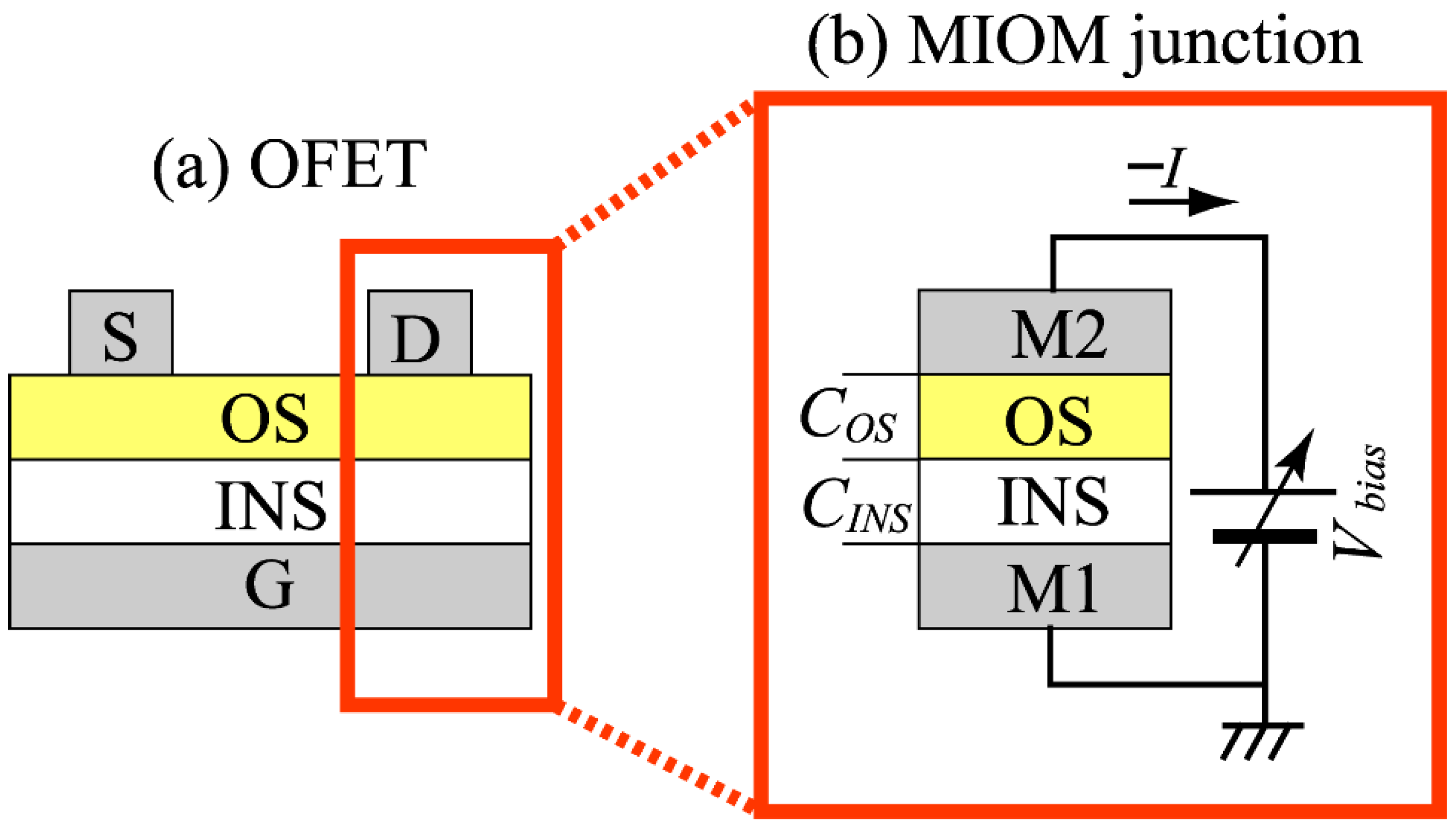
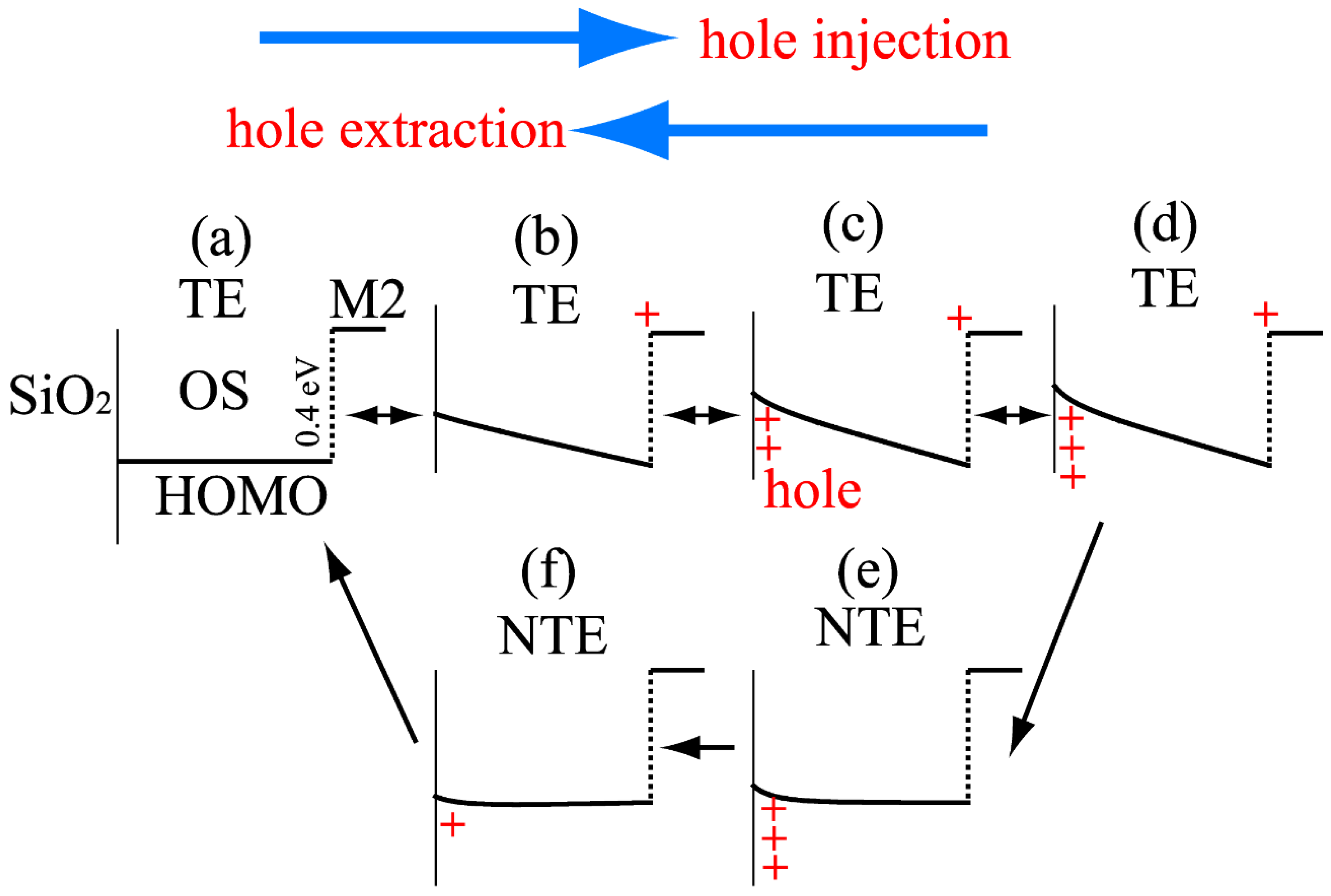
2. Concept of NTE Process of Charge Extraction

Figure 2 shows the calculations of potential distribution in the OS layer when a bias voltage, Vbias, is applied to an MIOM capacitor, with a hole injection barrier of 0.4 eV for the Schottky junction between the OS and M2. These calculations assume that there are no charge-capturing dopants in the OSs. This assumption is considered reasonable for OSs in which doping is difficult. Figure 2a–d show the potential diagrams of the thermal equilibrium (TE) state obtained by solving the Poisson–Boltzmann equation [13]. As there is a Schottky barrier at the OS/M2 interface, no charge is injected when Vbias is low (Figure 2b). The device operates as a capacitor with a series capacitance (C0) of the OS layer (COS) and INS layer (CINS), that is, C0 = CINSCOS/(CINS + COS). At this stage, the total accumulated charge Qtotal is the same as the interface charge Q0 between the OS and M2, that is, Qtotal = Q0 = C0Vbias. With an increase in Vbias, the gap between the Fermi level of the M2 electrode and the highest occupied molecular orbital (HOMO) near the INS decreased and holes were injected into the OS layer (Figure 2c,d). Consequently, the OS layer near the INS layer exhibited band bending owing to the accumulated holes. The degree of band bending increased as the amount of hole injection increased. However, this band bending is limited to the vicinity of the INS/OS interface, and the approximate shape of the potential curve in the OS layer is dominated by Q0 at the OS/M2 interface. The HOMO level of the OS at the OS/M2 interface was pinned by the Fermi level of M2 and did not exceed this level. Thus, once the holes were injected, most of the voltage applied to the capacitor decreased within the insulator layer.
Furthermore, we considered the charge extraction from this state by decreasing Vbias. If charge extraction occurs in the TE, it is the reverse of the charge injection case, with charge extraction at the INS/OS interface and then at the OS/M2 interface. However, as the electric field applied to the sample is still directed from the M2 electrode to the INS side, whether this TE reverse process occurs depends on carrier diffusion. If carrier diffusion is unlikely, the electric field in the OS, which is proportional to Q0, decreases rapidly before the charge is extracted from the INS/OS interface. This is the case for the NTE model [13]. When Q0 is slightly reversed, the charge at the INS/OS interface immediately begins to move because of the influence of the electric field. Therefore, the holes near the INS/OS interface are continuously extracted, whereas Q0 remains near zero, as shown in Figure 2e,f. Consequently, the initial state is achieved. In the NTE model, the potential in the NTE state is semiempirically reproduced based on the potential calculation in the TE state, considering the series of processes described above. States (e) and (f) are not in the TE but are kept metastable by the electric field. If an ohmic junction is formed at the OS/M2 interface, no such metastable state occurs, because the electric field near the OS/M2 interface is negligible. In other words, the formation of such a metastable state is unique to MIOM capacitors with Schottky junctions at the OS/M2 interface.
In the following section, experimental evidence supporting this model is presented.

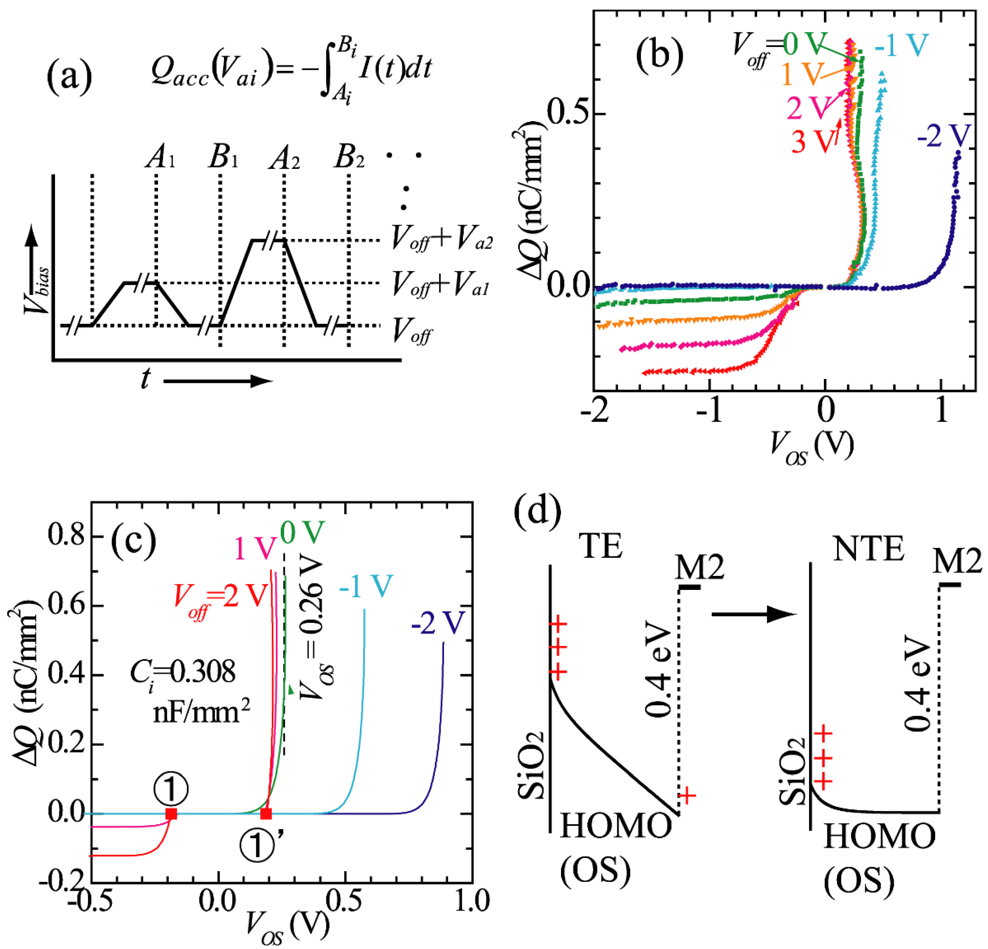
3. Experimental Evidences of NTE Charge Extraction

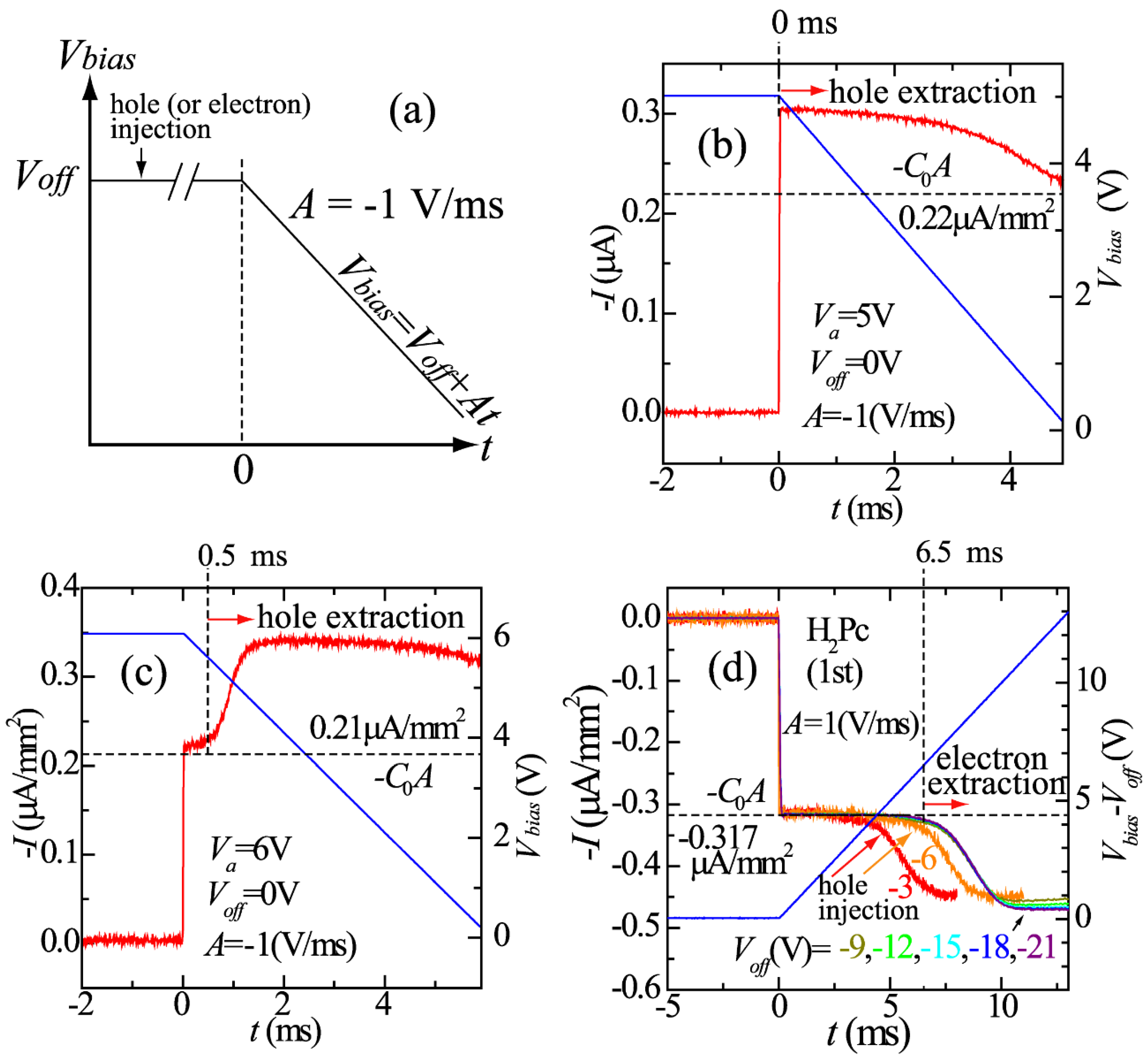
3.1. Displacement Current Measurement

The simplest experimental technique for detecting the NTE process during charge extraction is the displacement current measurement. Figure 3a shows the experimental setup. In this experiment, holes (or electrons) were injected through the Schottky barrier at the OS/M2 interface by applying a positive (or negative) Vbias at Voff for a long period. The injected holes (or electrons) were extracted using voltage sweeps.
Figure 3b shows a typical example of the displacement current used for hole extraction during the TE [13]. The sample used was n-Si/SiO2 (100 nm)/pentacene (50 nm)/Au. A sample behaved as a series capacitor if no charge was injected into (or extracted from) the OS layer. In that case, the displacement current is given by −I = −C0dVbias/dt, which is indicated by a dotted line in the figure. Here, C0 is the series capacitance of the INS and OS layers, as previously mentioned. If a current was observed above the dotted line, the accumulated charge near the INS/OS interface was extracted. In the pentacene sample (Figure 3b), the charge accumulated near the INS/OS interface was immediately extracted when the applied positive bias was reduced. This is direct evidence of the TE-type charge extraction in this sample.
Figure 3c shows a typical example of the displacement current used for hole extraction during the NTE. The sample was n-Si/SiO2 (100 nm)/metal-free phthalocyanine (H2Pc, 52 nm)/Au. The displacement current was close to C0dVbias/dt up to approximately t = 0.5 ms, and then increased sharply. This confirms that NTE charge extraction occurred, indicating that only the electric field in the OS layer changed in the first stage and that the holes injected at Vbias = Voff were extracted after the electric field inside the sample almost disappeared.
Currently, it is unclear whether charge carriers were extracted via the TE or NTE processes. However, considering the model shown in Figure 2, we believe that TE charge extraction was enhanced by diffusion processes and tended to occur when the carrier density or mobility was high. For the pentacene/Au sample, TE charge extraction was observed in many of the tested samples [13,15]; however, NTE charge extraction was also observed in some samples [18].
Figure 3d shows the electron extraction experiment for p-Si/SiO2 (70 nm)/H2Pc (44 nm)/Au [12]. Care must be taken when analyzing the data because the hole injection barrier was considerably lower than the electron injection barrier in H2Pc/Au. Figure 4 shows a potential diagram derived from the TE and NTE models to explain Figure 3d. In the case of Voff = −3 and −6 V, an electric field was generated in the OS layer, but no electrons were injected into the OS. A negative interfacial charge Q0 was generated at the OS/M2 interface because of the electric field (Figure 4a). When Vbias increased in the positive direction, Q0 decreased and eventually reversed, followed by hole injection. That is, a displacement current reflecting the change in Q0 was observed initially. Subsequently, a displacement current owing to hole injection was observed (Figure 4b,c).
In the case of Voff ≤ −9 V, electron injection at Vbias = Voff occurred (Figure 4d). In this Voff region, the time at which the displacement current began to decrease was almost constant at 6.5 ms (Figure 4e). This is because the voltage drop across the OS became constant when the electrons were injected. Therefore, it was possible to determine whether the electrons were injected by Voff based on the obtained experimental data. Although electrons were injected by Voff, the displacement current at the beginning of the voltage sweep was by C0 dVbias/dt. This indicated that the injected electrons were not extracted at the beginning of the voltage sweep, suggesting that NTE electron extraction occurred in this sample.

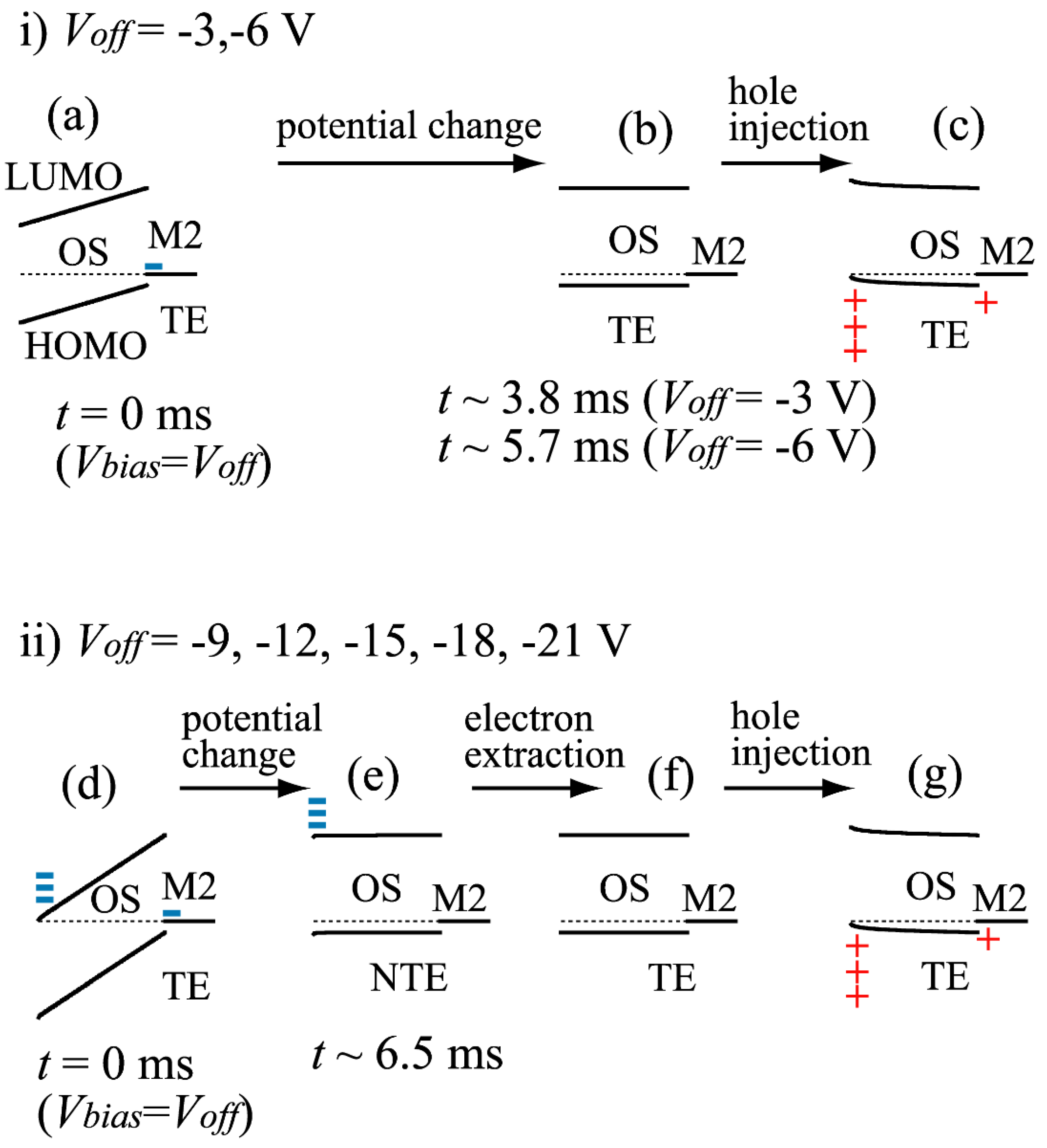
3.2. Accumulated Charge Measurement

Another method to investigate NTE charge extraction is ACM [12,13]. Changes in the accumulated charge are observed in this experiment. As the theoretical calculation of the accumulated charge is much easier than that of the displacement current, the observed data are analyzed more easily in this experiment than in the displacement current measurement.
Figure 5a shows the experimental scheme for the ACM. In this experiment, the states Vbias = Voff and Vbias = Va + Voff were alternately created to determine the amount of accumulated change Qacc (Va) = Qtotal (Va + Voff) − Qtotal (Voff). Here, Qtotal (Vbias) is the amount of charge accumulated at the junction when the applied voltage is maintained at Vbias for a long period. In the scheme shown in Figure 5a, long-term displacement current integration is necessary to determine Qacc (Va). However, as it is affected by the current amplifier offsets and other factors, Qacc (Va) is determined with high accuracy using a method called the voltage oscillation technique [14]. From the Qacc (Va) obtained thus, the parameters ΔQ and VOS were obtained using the following equations:
ΔQ = QaccC0 Va
VOS = VaQacc/CINS
These two parameters are defined as follows. The first is ΔQ, where C0Va is the accumulated charge at the OS/M2 interface; therefore, this parameter is zero when no charge is injected (or extracted) by Va into the OS and shifts from zero when charge is injected (or extracted). In addition, VOS indicates the voltage drop inside the OS caused by Va according to Gauss’s law. A feature of this experiment is that it is not dynamic, but static, and the experimentally obtained Qacc and Va as well as ΔQ and VOS are easy to compare with theoretical calculations that assume a quasistatic state.
Figure 5b shows the experimental data for ΔQ vs. VOS for n-Si/SiO2/H2Pc/Au during hole injection. The calculations of the ΔQVOS plots, assuming the NTE model, are shown in Figure 5c. The variation in the potential curve corresponding to point ① is shown in Figure 5d. This is the point where ΔQ shifts from zero, and according to calculations, a similar potential curve change occurs at point ①’. For OSs that follow the NTE model, the ΔQVOS plot allows us to determine the charge injection barrier at the OS/M2 interface experimentally. In the case of H2Pc/Au, the hole injection barrier with approximately 0.2 eV was obtained from the plot [13].

4. Conclusions

The NTE charge extraction described in this study is a phenomenon specific to an MIOM capacitor, where a Schottky barrier exists between the OS/M2 contacts and where the mobility of the OS is not very high. Several MIOM capacitors satisfy the above two conditions; consequently, the NTE process of charge extraction appears to be a common phenomenon in both MIOM capacitors and OFETs. In the case of MIS capacitors and inorganic field-effect transistors, where ohmic contacts are formed between the semiconductor and the metal electrode, this NTE process does not occur. This process in OFETs is detrimental to transistor operation. Considering the mechanism of the process, the fabrication of ohmic contacts between the OS/M2 interface or the application of an OS with high mobility are the most effective ways to avoid this process. However, the NTE process may be useful in the application of OFETs, as memory devices. In addition, the NTE phenomenon can be used to determine the charge injection (extraction) barrier by means of ACM [12,13].

Author Contributions

This study was conceptualized by H.T. The formal analysis and methodology were provided by H.T. and T.O. Data curation was conducted by T.K. All authors have read and agreed to the published version of the manuscript.

Funding

This study was supported by a Grant-in-Aid for Scientific Research (Grant no. 21K05009).

Data Availability Statement

Data will be made available upon request.

Conflicts of Interest

The authors declare no conflict of interest.

References

  1. Horowits, G. Organic Field-effect transistors. Adv. Mater. 1999, 10, 365–377. [Google Scholar] [CrossRef]
  2. Sirringhaus, H. Organic Field-effect transistors. The pass beyond amorphous silicon. Adv. Mater. 2014, 26, 1319–1335. [Google Scholar] [CrossRef] [PubMed] [Green Version]
  3. Lamport, Z.A.; Haneef, H.F.; Anand, S.; Waldrip, M.; Jurchescu, O.D. Tutorial: Organic field-effect transistors: Material, structure and operation. J. Appl. Phys. 2018, 8, 071101. [Google Scholar] [CrossRef]
  4. Sze, S.M.; Ng, K.K. Physics of Semiconductor Devices, 3rd ed.; John Wiley & Sons, Inc.: Hoboken, NJ, USA, 2007. [Google Scholar]
  5. Kim, S.; Yoo, H.; Choi, J. Effects of charge traps on hysteresis in organic field-effect transistors and their charge trap cause analysis through causal inference techniques. Sensor 2023, 23, 2265. [Google Scholar] [CrossRef] [PubMed]
  6. Egginger, M.; Bauer, S.; Schwdiauer, R.; Neugebauer, H.; Sariciftci, N.S. Current versus gate voltage hysteresis in organic field effect transistors. Mon. Chem. 2009, 140, 735–750. [Google Scholar] [CrossRef]
  7. Park, Y.; Baeg, K.; Kim, C. Solution-processed nonvolatile organic transistor memory based on semiconductor blend. ACS Appl. Mater. Interfaces 2019, 11, 8327–8336. [Google Scholar] [CrossRef] [PubMed]
  8. Wang, W.V.; Zhang, Y.; Li, X.; Chen, Z.; Wu, Z.; Zhang, L.; Lin, Z.; Zhang, H. High performance nonvolatile organic field-effect transistor memory devices based on pyrene diimide derivative. InfoMat 2021, 3, 814–822. [Google Scholar] [CrossRef]
  9. Yu, T.; Liu, Z.; Wang, Y.; Zhang, L.; Hou, S.; Wan, Z.; Yin, J.; Gao, X.; Wu, L.; Xia, Y.; et al. Deep-trap dominated degradation of the endurance characteristics in OFET memory with polymer charge-trapping layer. Sci. Rep. 2023, 13, 5865. [Google Scholar] [CrossRef]
  10. Park, S.; Kim, S.H.; Choi, H.H.; Kang, B.; Cho, K. Recent advances in the bias stress stability of organic transistors. Adv. Funct. Mater. 2020, 30, 1904590. [Google Scholar] [CrossRef]
  11. Hu, Y.; Zheng, L.; Li, J.; Huang, Y.; Wang, Z.; Lu, X.; Yu, L.; Wang, S.; Sun, Y.; Ding, S.; et al. Organic phase-change memory transistor based on an organic semiconductor with reversible molecular conformation transition. Adv. Sci. 2023, 10, 2205694. [Google Scholar] [CrossRef]
  12. Oda, T.; Yamaguchi, K.; Kadoya, T.; Tajima, H. Measurement of electron injection barriers in OS/Au (OS = phthalocyanine and pentacene) using accumulated charge measurement. Org. Electron. 2023, 120, 106827. [Google Scholar] [CrossRef]
  13. Tajima, H.; Kadoya, T.; Yamaguchi, K.; Omura, Y.; Oda, T.; Ogino, A. Thermal and non-thermal equilibrium processes of charge extraction in accumulated charge measurement (ACM). J. Appl. Phys. 2021, 130, 195501. [Google Scholar] [CrossRef]
  14. Tajima, H.; Miyao, F.; Mizukoshi, M.; Sato, S. Determination of charge injection barrier using the displacement current measurement technique. Org. Electron. 2016, 34, 193–199. [Google Scholar] [CrossRef]
  15. Kadoya, T.; Otsuka, M.; Ogino, A.; Sato, S.; Yokomatsu, T.; Maenaka, K.; Yamada, J.; Tajima, H. Estimation of charge-Injection barriers at the metal/Pentacene interface through accumulated charge measurement. J. Phys. Chem. C 2017, 121, 2882–2888. [Google Scholar] [CrossRef]
  16. Tajima, H.; Yoshida, K.; Sato, S.; Kadoya, T.; Yamada, J. Estimation of the charge injection barrier at a metal/organic semiconductor interface based on accumulated charge measurement: The effect of offset bias voltages. J. Phys. Chem. C 2017, 121, 14725–14730. [Google Scholar] [CrossRef]
  17. Tajima, H.; Yasukawa, N.; Nakatani, H.; Sato, S.; Kadoya, T.; Yamada, J. Estimation of hole injection barrier at the poly-3(hexylthiophene)/metal interface using accumulated charge measurement. Org. Electron. 2017, 51, 162–167. [Google Scholar] [CrossRef]
  18. Tanimura, T.; Tajima, H.; Ogino, A.; Miyamoto, Y.; Kadoya, T.; Komino, T.; Yokomatsu, T.; Maenaka, K.; Ikemoto, Y. Accumulated charge measurement using a substrate with a restricted-bottom-electrode structure. Org. Electron. 2019, 74, 251–257. [Google Scholar] [CrossRef]
  19. Shimomoto, S.; Kadoya, T.; Tanimura, T.; Maenaka, K.; Yokomatsu, T.; Komino, T.; Tajima, H. Accumulated charge measurement: Control of the interfacial depletion layer by offset voltage and estimation of band gap and electron injection barrier. J. Phys. Chem. C 2021, 125, 1990–1998. [Google Scholar] [CrossRef]
  20. Ishii, H.; Sugiyama, K.; Ito, E.; Seki, K. Energy Level Alignment and Interfacial Electronic Structures at Organic/Metal and Organic/Organic Interfaces. Adv. Mater. 1999, 11, 605–625. [Google Scholar] [CrossRef]
  21. Hill, I.G.; Milliron, D.; Schwartz, J.; Kahn, A. Organic semiconductor interfaces: Electronic structure and transport properties. Appl. Surf. Sci. 2000, 166, 354. [Google Scholar] [CrossRef]
  22. Adachi, C.; Oyamada, T.; Nakajima, Y. Data Book on Work Function of Organic-Thin Films, 2nd ed.; CMC International: Tokyo, Japan, 2006. [Google Scholar]
  23. Kirihata, H.; Uda, M. Externally quenched air counter for low-energy electron emission measurements. Rev. Sci. Instrum. 1981, 52, 68–70. [Google Scholar] [CrossRef]
  24. Zahn, D.R.T.; Gavrila, G.N.; Georgoi, M. The transport gap of organic semiconductors studied using the combination of direct and inverse photoemission. Chem. Phys. 2006, 325, 99–112. [Google Scholar] [CrossRef]
  25. Yoshida, H. Near-ultraviolet inverse photoemission spectroscopy using ultra-lowenergy electrons. Chem. Phys. Lett. 2012, 180, 539–540. [Google Scholar]
Figure 2. Schematic potential curve to explain the hole injection and extraction processes in the MIOM junction, where a Schottky contact of 0.4 eV is formed between the HOMO of the OS and M2 electrode. The layers of M1 and INS (SiO2) and the potential curve of LUMO are omitted for simplicity in the figures. A flat band state is shown in (a). A positive bias voltage is applied to the M2 electrode. The potential curves (ad) are obtained for the TE state. The curves (e,f) are realized in the NTE state when the charges at the OS/M2 interface are extracted before the holes near the INS/OS boundary are extracted.
Magnetochemistry 09 00180 g002
Figure 3. Displacement current (I) measurements as a function of time (t) to investigate the NTE process in an MIOM capacitor. (a) Schematic of the applied bias voltage (Vbias) pattern. Vbias is maintained at Voff for a long time to inject holes (or electrons) into the OS and then decreased at a rate of A above t = 0 ms. (b) Measurement for n-Si/SiO2 (100 nm)/pentacene (50 nm)/Au. The value of I at t = 0 ms exceeds −C0A, suggesting that TE-type hole extraction occurs in this sample. (c) Measurement for n-Si/SiO2 (100 nm)/H2Pc (52 nm)/Au. The value of I below t = 0.5 ms approximately coincides with −C0A, suggesting that NTE-type hole extraction occurs in this sample. (d) Measurement for p-Si/SiO2(70 nm)/H2Pc (44 nm)/Au. For Voff = −3 and −6 V, electron injection does not occur and the changes in I around t = 3.8 ms (Voff = −3 V) and 5.7 ms (Voff = −6 V) are due to the injection of holes. For Voff = −9, −12, −15, −18, and −21 V, electron injection occurs. The changes in I around t = 6.5 ms are due to the extraction of electrons. Hole injection subsequently occurs after the extraction. (See the text and Figure 4 for details.). Panels (b,c) were reproduced and modified with permissions [13]. Copyright © 2021, AIP Publishing. Panel (d) was reproduced with permission [12]. Copyright © 2023, Elsevier B. V.
Magnetochemistry 09 00180 g003
Figure 4. Potential diagram to explain the displacement current of p-Si/SiO2/H2Pc/Au shown in Figure 3d. The layers of M1 and INS (SiO2) are omitted for simplicity in the figure. At Voff = −3 and −6 V, Vbias = Voff is insufficient to inject electrons (a). The threshold of the decrease in displacement current is due to the hole injection from M2 to the OS (b,c). At Voff = −9, −12, −15, −18, and −21 V, the time dependence of the displacement current is almost the same, and the displacement current at t < 6.5 ms is approximately −C0A. This is the direct evidence indicating electron injection by Voff (d) and the NTE process of electron extraction (d)→(e). As the voltage drops in the OS layer at Vbias = Voff are almost the same owing to the electron accumulation near the INS/OS interface, the thresholds of the current decrease are also almost the same. After the electrons are extracted (e)→(f), holes are subsequently injected (f)→(g).
Magnetochemistry 09 00180 g004
Figure 5. Experimental evidence of the NTE model for charge extraction based on ACM. (a) Schematic of applied bias voltage (Vbias) as a function of time (t). Vbias is a combination of the constant voltage Voff and the alternating voltage Va. Qacc as a function of Va is obtained by integrating the displacement current from Ai to Bi. From the obtained dataset of Qacc and Va, ΔQ and VOS are obtained using Equations (1) and (2) in the text. ΔQ indicates whether charges are injected into the OS layer, and VOS is the potential change within the OS layer caused by Va. (b) Experimentally obtained ΔQVOS plot for hole injection in the MIOM capacitor of n-Si/SiO2 (100 nm)/H2Pc (52 nm)/Au. (c) Calculation of ΔQVOS plot based on the NTE model. (d) Change in the potential curves associated with the point ① in (c). The layers of M1, INS (SiO2) as well as the potential curve of LUMO are omitted in the figures for simplicity. Panel (a) was reproduced with permission [12]. Copyright © 2023, Elsevier B. V. Panels (b,c) were reproduced with permissions [13]. Copyright © 2021, AIP Publishing.
Magnetochemistry 09 00180 g005
Disclaimer/Publisher’s Note: The statements, opinions and data contained in all publications are solely those of the individual author(s) and contributor(s) and not of MDPI and/or the editor(s). MDPI and/or the editor(s) disclaim responsibility for any injury to people or property resulting from any ideas, methods, instructions or products referred to in the content.

