

Ferroelectric Polarization in an h-BN-Encapsulated 30°-Twisted Bilayer–Graphene Heterostructure

Abstract
:1. Introduction
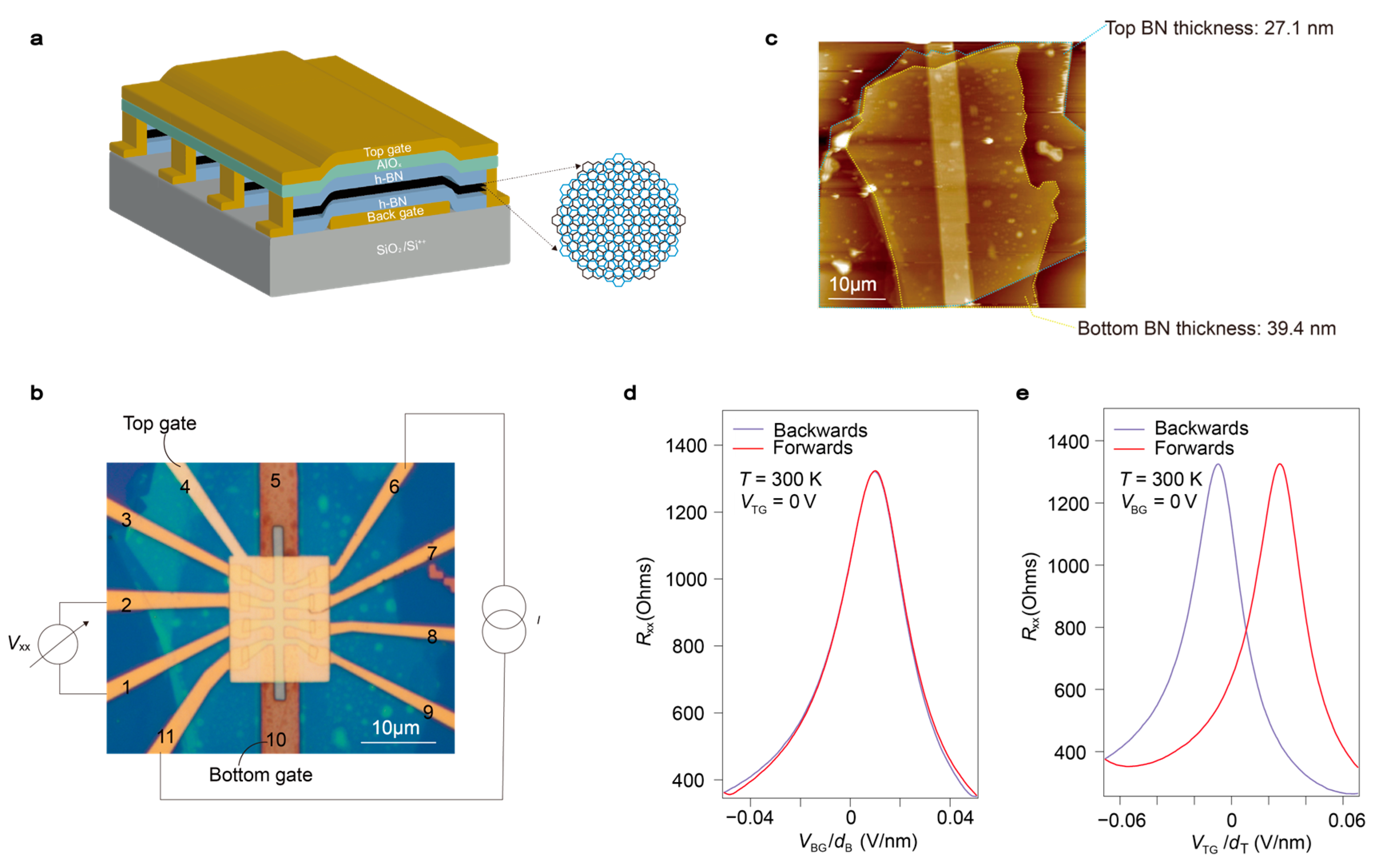
2. Methods
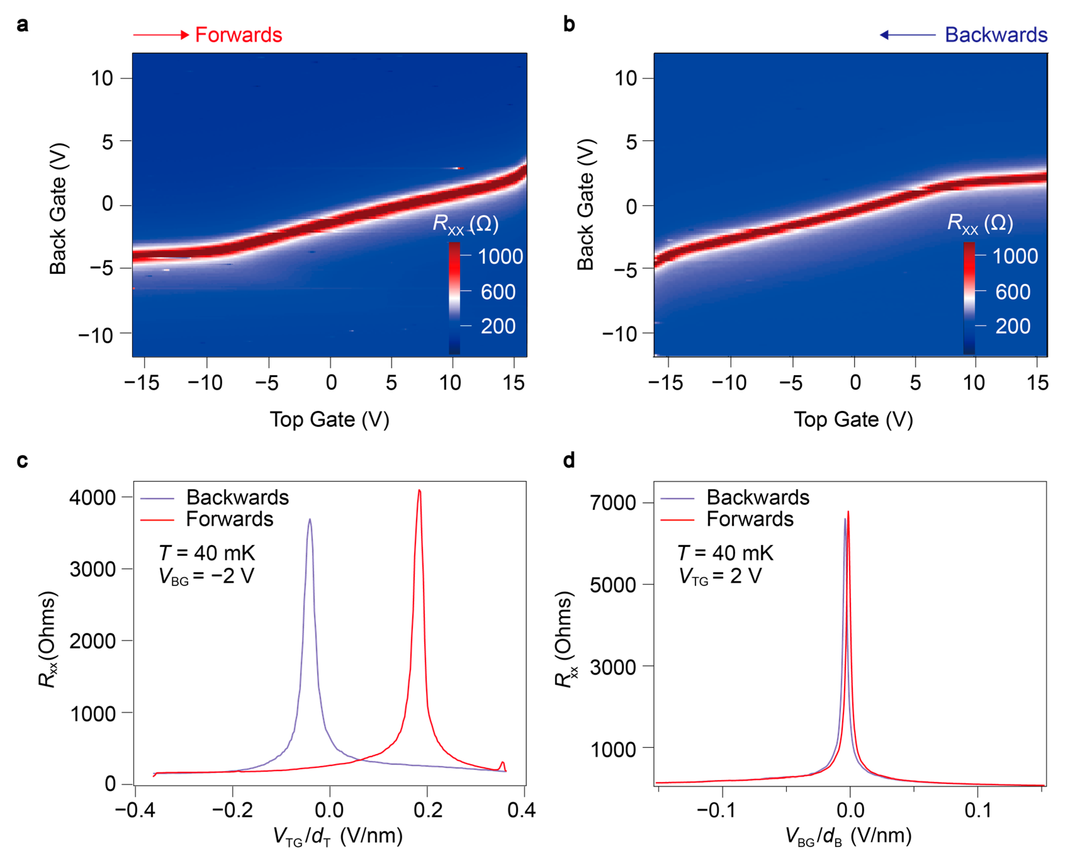
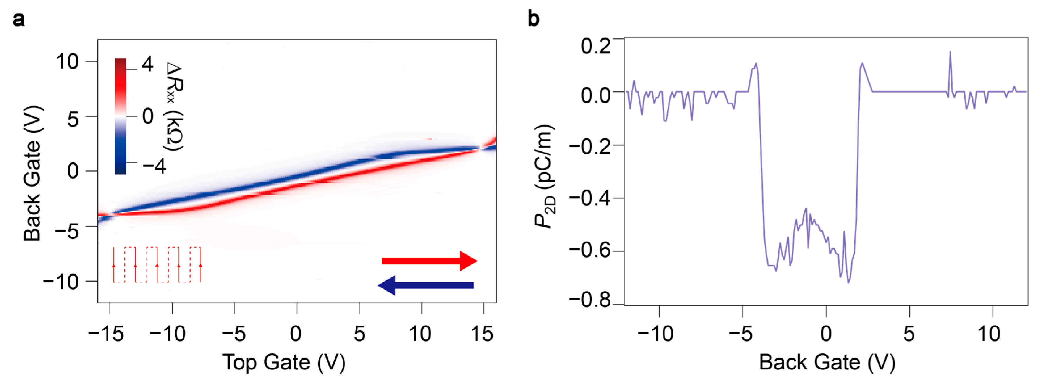
3. Results and Discussion
4. Conclusions
Supplementary Materials
Author Contributions
Funding
Institutional Review Board Statement
Informed Consent Statement
Data Availability Statement
Acknowledgments
Conflicts of Interest
References
- Martin, L.W.; Rappe, A.M. Thin-film ferroelectric materials and their applications. Nat. Rev. Mater. 2016, 2, 16087. [Google Scholar] [CrossRef]
- Bertolazzi, S.; Bondavalli, P.; Roche, S.; San, T.; Choi, S.Y.; Colombo, L.; Bonaccorso, F.; Samorì, P. Nonvolatile memories based on graphene and related 2D materials. Adv. Mater. 2019, 31, 1806663. [Google Scholar] [CrossRef] [PubMed]
- Khan, A.I.; Keshavarzi, A.; Datta, S. The future of ferroelectric field effect transistor technology. Nat. Electron. 2020, 3, 588–597. [Google Scholar] [CrossRef]
- Wang, X.; Yasuda, K.; Zhang, Y.; Liu, S.; Watanabe, K.; Taniguchi, T.; Hone, J.; Fu, L.; Jarillo-Herrero, P. Interfacial ferroelectricity in rhombohedral-stacked bilayer transition metal dichalcogenides. Nat. Nanotechnol. 2022, 17, 367–371. [Google Scholar] [CrossRef] [PubMed]
- Wu, M.; Li, J. Sliding ferroelectricity in 2D van der Waals materials: Related physics and future opportunities. Proc. Natl. Acad. Sci. USA 2021, 118, e2115703118. [Google Scholar] [CrossRef]
- Zhou, Y.; Wu, D.; Zhu, Y.; Cho, Y.; He, Q.; Yang, X.; Herrera, K.; Chu, Z.; Han, Y.; Downer, M.C.; et al. Out-of-Plane Piezoelectricity and Ferroelectricity in Layered α-In2Se3 Nanoflakes. Nano Lett. 2017, 17, 5508–5513. [Google Scholar] [CrossRef]
- Cui, C.; Hu, W.J.; Yan, X.; Addiego, C.; Gao, W.; Wang, Y.; Wang, Z.; Li, L.; Cheng, Y.; Li, P.; et al. Intercorrelated In-Plane and Out-of-Plane Ferroelectricity in Ultrathin Two-Dimensional Layered Semiconductor In2Se3. Nano Lett. 2018, 18, 1253–1258. [Google Scholar] [CrossRef]
- Liu, F.; You, L.; Seyler, K.L.; Li, X.; Yu, P.; Lin, J.; Wang, X.; Zhou, J.; Wang, H.; He, H.; et al. Room-temperature ferroelectricity in CuInP2S6 ultrathin flakes. Nat. Commun. 2016, 7, 12357. [Google Scholar] [CrossRef]
- Belianinov, A.; He, Q.; Dziaugys, A.; Maksymovych, P.; Eliseev, E.; Borisevich, A.; Morozovska, A.; Banys, J.; Vysochanskii, Y.; Kalinin, S.V. CuInP2S6 Room Temperature Layered Ferroelectric. Nano Lett. 2015, 15, 3808–3814. [Google Scholar] [CrossRef]
- Jiang, X.; Wang, X.; Wang, X.; Zhang, X.; Niu, R.; Deng, J.; Xu, S.; Lun, Y.; Liu, Y.; Xia, T.; et al. Manipulation of current rectification in van der Waals ferroionic CuInP2S6. Nat. Commun. 2022, 13, 574. [Google Scholar] [CrossRef]
- Chang, K.; Liu, J.; Lin, H.; Wang, N.; Zhao, K.; Zhang, A.; Jin, F.; Zhong, Y.; Hu, X.; Duan, W.; et al. Discovery of robust in-plane ferroelectricity in atomic-thick SnTe. Science 2016, 353, 274–278. [Google Scholar] [CrossRef]
- Zheng, C.; Yu, L.; Zhu, L.; Collins, J.L.; Kim, D.; Lou, Y.; Xu, C.; Li, M.; Wei, Z.; Zhang, Y.; et al. Room temperature in-plane ferroelectricity in van der Waals In2Se3. Sci. Adv. 2018, 4, eaar7720. [Google Scholar] [CrossRef]
- Higashitarumizu, N.; Kawamoto, H.; Lee, C.J.; Lin, B.H.; Chu, F.H.; Yonemori, I.; Nishimura, T.; Wakabayashi, K.; Chang, W.H.; Nagashio, K. Purely in-plane ferroelectricity in monolayer SnS at room temperature. Nat. Commun. 2020, 11, 2428. [Google Scholar] [CrossRef]
- Wang, Y.; Li, W.; Guo, Y.; Huang, X.; Luo, Z.; Wu, S.; Wang, H.; Chen, J.; Li, X.; Zhan, X.; et al. A gate-tunable artificial synapse based on vertically assembled van der Waals ferroelectric heterojunction. J. Mater. Sci. Technol. 2022, 128, 239–244. [Google Scholar] [CrossRef]
- Li, W.; Guo, Y.; Luo, Z.; Wu, S.; Han, B.; Hu, W.; You, L.; Watanabe, K.; Taniguchi, T.; Alava, T.; et al. A Gate Programmable van der Waals Metal-Ferroelectric-Semiconductor Vertical Heterojunction Memory. Adv. Mater. 2022, 35, 2208266. [Google Scholar] [CrossRef]
- Zheng, Z.; Ma, Q.; Bi, Z.; de La Barrera, S.; Liu, M.H.; Mao, N.; Zhang, Y.; Kiper, N.; Watanabe, K.; Taniguchi, T.; et al. Unconventional ferroelectricity in moiré heterostructures. Nature 2020, 588, 71–76. [Google Scholar] [CrossRef]
- Yasuda, K.; Wang, X.; Watanabe, K.; Taniguchi, T.; Jarillo-Herrero, P. Stacking-engineered ferroelectricity in bilayer boron nitride. Science 2021, 372, 1458–1462. [Google Scholar] [CrossRef]
- Vizner, S.M.; Waschitz, Y.; Cao, W.; Nevo, I.; Watanabe, K.; Taniguchi, T.; Sela, E.; Urbakh, M.; Hod, O.; Ben Shalom, M. Interfacial ferroelectricity by van der Waals sliding. Science 2021, 372, 1462–1466. [Google Scholar] [CrossRef]
- Woods, C.R.; Ares, P.; Nevison-Andrews, H.; Holwill, M.J.; Fabregas, R.; Guinea, F.; Geim, A.K.; Novoselov, K.S.; Walet, N.R.; Fumagalli, L. Charge-polarized interfacial superlattices in marginally twisted hexagonal boron nitride. Nat. Commun. 2021, 12, 347. [Google Scholar] [CrossRef]
- Niu, R.; Li, Z.; Han, X.; Qu, Z.; Ding, D.; Wang, Z.; Liu, Q.; Liu, T.; Han, C.; Watanabe, K.; et al. Giant ferroelectric polarization in a bilayer graphene heterostructure. Nat. Commun. 2022, 13, 6241. [Google Scholar] [CrossRef]
- Shen, C.; Chu, Y.; Wu, Q.; Li, N.; Wang, S.; Zhao, Y.; Tang, J.; Liu, J.; Tian, J.; Watanabe, K.; et al. Correlated states in twisted double bilayer graphene. Nat. Phys. 2020, 16, 520–525. [Google Scholar] [CrossRef]
- Park, J.M.; Cao, Y.; Watanabe, K.; Taniguchi, T.; Jarillo-Herrero, P. Tunable strongly coupled superconductivity in magic-angle twisted trilayer graphene. Nature 2021, 590, 249–255. [Google Scholar] [CrossRef] [PubMed]
- Cao, Y.; Rodan-Legrain, D.; Rubies-Bigorda, O.; Park, J.M.; Watanabe, K.; Taniguchi, T.; Jarillo-Herrero, P. Tunable correlated states and spin-polarized phases in twisted bilayer–bilayer graphene. Nature 2020, 583, 215–220. [Google Scholar] [CrossRef]
- Liu, X.; Hao, Z.; Khalaf, E.; Lee, J.Y.; Ronen, Y.; Yoo, H.; Haei Najafabadi, D.; Watanabe, K.; Taniguchi, T.; Vishwanath, A.; et al. Tunable spin-polarized correlated states in twisted double bilayer graphene. Nature 2020, 583, 221–225. [Google Scholar] [CrossRef] [PubMed]
- Arora, H.S.; Polski, R.; Zhang, Y.; Thomson, A.; Choi, Y.; Kim, H.; Lin, Z.; Wilson, I.Z.; Xu, X.; Chu, J.H.; et al. Superconductivity in metallic twisted bilayer graphene stabilized by WSe2. Nature 2020, 583, 379–384. [Google Scholar] [CrossRef]
- Klein, D.R.; Xia, L.Q.; MacNeill, D.; Watanabe, K.; Taniguchi, T.; Jarillo-Herrero, P. Electrical switching of a bistable moiré superconductor. Nat. Nanotechnol. 2023, 30, 331–335. [Google Scholar] [CrossRef]
- Yao, W.; Wang, E.; Bao, C.; Zhang, Y.; Zhang, K.; Bao, K.; Chan, C.K.; Chen, C.; Avila, J.; Asensio, M.C.; et al. Quasicrystalline 30 twisted bilayer graphene as an incommensurate superlattice with strong interlayer coupling. Proc. Natl. Acad. Sci. USA 2018, 115, 6928–6933. [Google Scholar] [CrossRef]
- Sanchez-Yamagishi, J.D.; Taychatanapat, T.; Watanabe, K.; Taniguchi, T.; Yacoby, A.; Jarillo-Herrero, P. Quantum Hall effect, screening, and layer-polarized insulating states in twisted bilayer graphene. Phys. Rev. Lett. 2012, 108, 076601. [Google Scholar] [CrossRef]
- Ahn, S.J.; Moon, P.; Kim, T.H.; Kim, H.W.; Shin, H.C.; Kim, E.H.; Cha, H.W.; Kahng, S.J.; Kim, P.; Koshino, M.; et al. Dirac electrons in a dodecagonal graphene quasicrystal. Science 2018, 361, 782–786. [Google Scholar] [CrossRef]
- Spurrier, S.; Cooper, N.R. Theory of quantum oscillations in quasicrystals: Quantizing spiral Fermi surfaces. Phys. Rev. B 2019, 100, 081405. [Google Scholar] [CrossRef]
- Sun, X.; Zhang, S.; Liu, Z.; Zhu, H.; Huang, J.; Yuan, K.; Wang, Z.; Watanabe, K.; Taniguchi, T.; Li, X.; et al. Correlated states in doubly-aligned hBN/graphene/hBN heterostructures. Nat. Commun. 2021, 12, 7196. [Google Scholar] [CrossRef] [PubMed]
- Wang, Y.; Gao, X.; Yang, K.; Gu, P.; Lu, X.; Zhang, S.; Gao, Y.; Ren, N.; Dong, B.; Jiang, Y.; et al. Quantum Hall phase in graphene engineered by interfacial charge coupling. Nat. Nanotechnol. 2022, 17, 1272–1279. [Google Scholar] [CrossRef] [PubMed]
- Saito, Y.; Ge, J.; Watanabe, K.; Taniguchi, T.; Young, A.F. Independent superconductors and correlated insulators in twisted bilayer graphene. Nat. Phys. 2020, 16, 926–930. [Google Scholar] [CrossRef]
- Lin, J.X.; Zhang, Y.H.; Morissette, E.; Wang, Z.; Liu, S.; Rhodes, D.; Watanabe, K.; Taniguchi, T.; Hone, J.; Li, J.I. Spin-orbit–driven ferromagnetism at half moiré filling in magic-angle twisted bilayer graphene. Science 2022, 375, 437–441. [Google Scholar] [CrossRef]


Disclaimer/Publisher’s Note: The statements, opinions and data contained in all publications are solely those of the individual author(s) and contributor(s) and not of MDPI and/or the editor(s). MDPI and/or the editor(s) disclaim responsibility for any injury to people or property resulting from any ideas, methods, instructions or products referred to in the content. |
© 2023 by the authors. Licensee MDPI, Basel, Switzerland. This article is an open access article distributed under the terms and conditions of the Creative Commons Attribution (CC BY) license (https://creativecommons.org/licenses/by/4.0/).
Share and Cite
Ren, L.; Dong, B. Ferroelectric Polarization in an h-BN-Encapsulated 30°-Twisted Bilayer–Graphene Heterostructure. Magnetochemistry 2023, 9, 116. https://doi.org/10.3390/magnetochemistry9050116
Ren L, Dong B. Ferroelectric Polarization in an h-BN-Encapsulated 30°-Twisted Bilayer–Graphene Heterostructure. Magnetochemistry. 2023; 9(5):116. https://doi.org/10.3390/magnetochemistry9050116
Chicago/Turabian StyleRen, Lingling, and Baojuan Dong. 2023. "Ferroelectric Polarization in an h-BN-Encapsulated 30°-Twisted Bilayer–Graphene Heterostructure" Magnetochemistry 9, no. 5: 116. https://doi.org/10.3390/magnetochemistry9050116