Article

Carbon Nanotubes Use for the Semiconductors ZnSe and ZnS Material Surface Modification via the Laser-Oriented Deposition Technique

1
Lab for Photophysics of Media with Nanoobjects at Vavilov State Optical Institute, Kadetskaya Liniya V.O., Dom 5, Korp.2/Babushkina Str., Dom 36, Korp.1, 199053 St. Petersburg, Russia
2
Photonica Department, St. Petersburg Electrotechnical University (“LETI”), Ul.Prof.Popova, Dom 5, 197376 St. Petersburg, Russia
3
Petersburg Nuclear Physics Institute, National Research Center “Kurchatov Institute”, 1 md. Orlova Roshcha, 188300 Gatchina, Russia
4
Moscow Institute of Physics and Technology (National Research University), 9 Institutskiy per., Dolgoprudny, 141701 Moscow, Russia
5
Emanuel Institute of Biochemical Physics RAS, 4 Kosigina St., 119334 Moscow, Russia
6
Physics and Mathematics Department, Pirogov Russian National Research Medical University, Ostrovitianov Str. 1, 117997 Moscow, Russia
*
Author to whom correspondence should be addressed.
Submission received: 16 November 2021 / Revised: 3 December 2021 / Accepted: 4 December 2021 / Published: 7 December 2021

Abstract

:
It is known that a material’s volume and the surface structuring by the nanoparticles causes a significant change in the material’s basic properties. In this aspect, the structuration of the surface of semiconductors is of interest, because their wide potential application in optoelectronics can extend the products’ transparency, hardness, wettability, and other important parameters. This paper presents possible methods for the surface modification of zinc selenide and zinc sulfide when carbon nanotubes are deposited on the surface by the application of the laser-oriented technique. It also shows changes of the spectral, mechanical, and wetting characteristics of the considered materials. Using the molecular dynamic simulations, the possible process of the carbon nanotubes penetration into the considered surfaces is presented. The simulation results are partially supported by the obtained experimental data.

1. Introduction

Among the different materials involved in general optoelectronics, semiconductor materials occupy a special place that is connected with the unique charge carrier mobility of the semiconductor structures and their operation in the visible and near-IR spectral range. These structures can be involved in the solar energy, gas storage, modulation, optical limiting, etc. schemes as well, and they can dramatically extend the applications of optoelectronics devices [1,2,3,4]. ZnSe and ZnS materials can be considered as perspective semiconductors to form the different detectors for the wide spectral range and to develop the mirrors and the optical limiting instruments [5,6,7,8,9,10,11,12,13,14,15,16,17]. Researchers have revealed the anti-reflective, luminescent properties of these materials and visualized the process of the nanoparticles’ creation based on the ZnSe and ZnS structures and their introduction into the polymer matrices [8,9,10,11]. Treatment of these materials by femtosecond lasers has been explained as well [12,16].
Furthermore, it should be remarked that ZnSe and ZnS materials are widely used to make the electrically and optically addressed spatial light modulators (SLM), which operate in the blue and in the visible spectral range. This specific application is connected with the high carrier mobility of these types of the materials. Thus, the response (switch-on and switch-off time) can be revealed with good speed. Indeed, the resolution of the SLM with the photo layers based on the ZnSe and ZnS structures is not so good. However, the compromise between the resolution and the speed can be found via the specific pulsed regime of the laser operations when the delay between the electric pulse and the light one can be varied [17,18].
Different types of classical methods and innovative approaches can be used in order to modify the interface and the surface of the semiconductor materials with the nanoparticles. As promising nano-objects used for this aim, carbon nanotubes (CNTs) [19,20,21,22,23,24] can be successfully proposed. The basic features of the carbon nanotubes are regarded to be their branched surface, their high conductivity, the strong hardness of their C–C bonds, the little value of the refractive index as well as their complicated and unique mechanisms of the charge carrier moving.
In the current paper, the laser-oriented deposition (LOD) approach, previously shown to treat inorganic crystals and metals, such as KBr [25], BaF2 [26], and Al [27], is shown as the perspective instrument to modify the properties of the semiconductors based on ZnSe and ZnS. The possibility of the ZnS and ZnSe surfaces’ modification via the vertically oriented CNTs deposition is shown. Modification leads to changes in the atomic structure of the surface as well as the mechanical and the optical properties. The obtained modified structures show prospects for an application as a basic element of the optoelectronics schemes, of the solar cells, and of the gas storage systems. Moreover, it can be useful for information technology and displays.

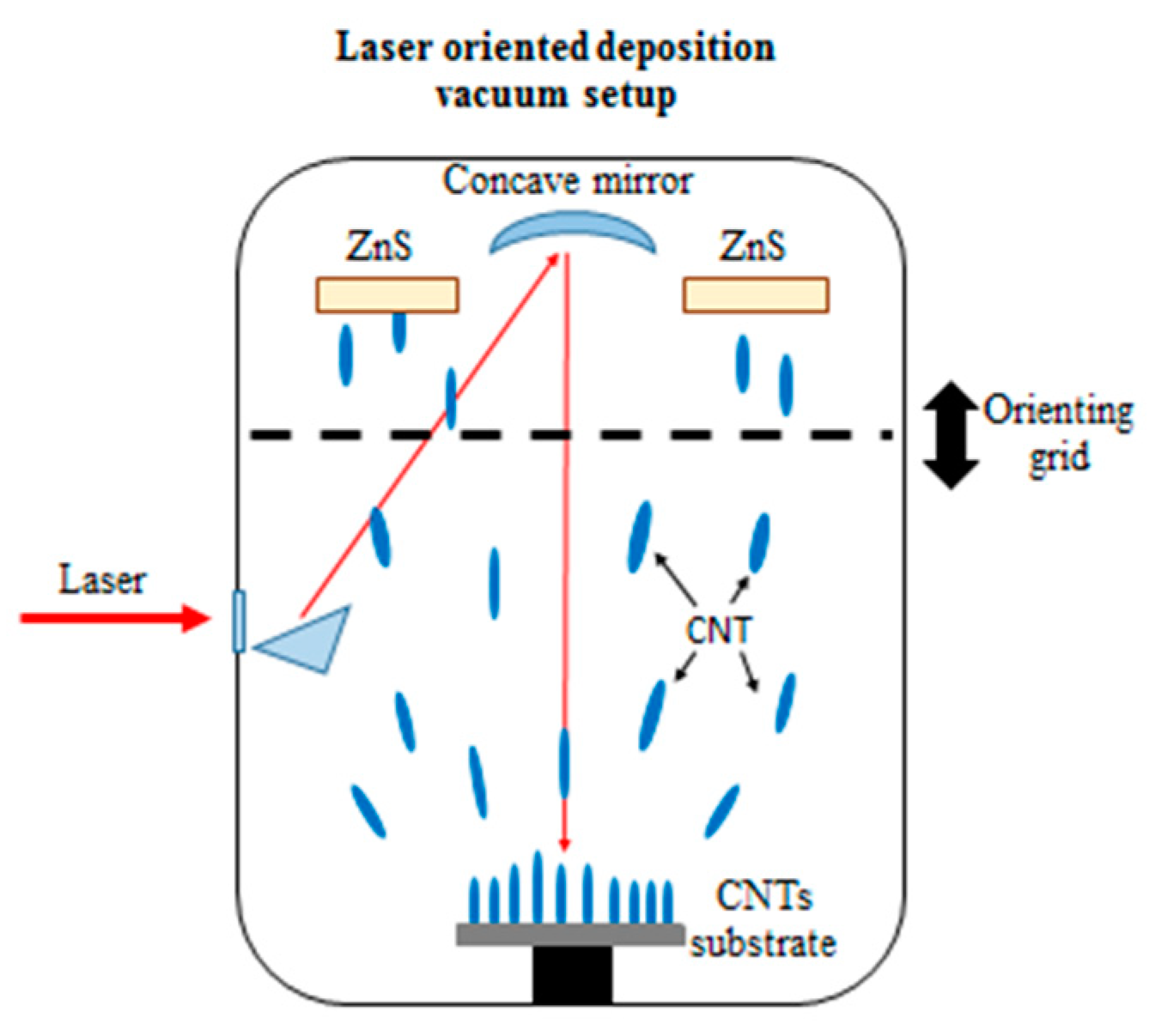
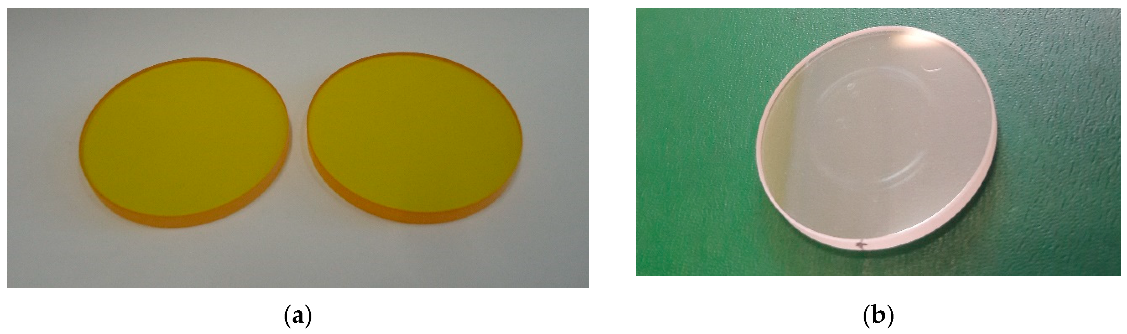
2. Materials and Methods

The matrix ZnSe and ZnS materials have been purchased from the “Alkor Technologies” company in Saint-Petersburg. The diameter of the substrate was 35 mm and the thickness of the ZnSe and ZnS structures was 5 and 3 mm, respectively.
To modify the properties of the semiconductor materials via their surface treatment, the single-wall carbon nanotubes (SWCNTs) type #704121 with the diameter placed in the range of 0.7–1.1 nm purchased from Aldrich Co. have been used. It is important in order to find the coinciding conditions between the dimensions of the CNTs directly with the elementary lattice of the material.
To modify the surface, the IR CO2 laser with p-polarized irradiation at the wavelength of 10.6 μm and the power of 30 W has been used. The general view of the block scheme has been shown in [25]. It is shown that the laser system was connected with a vacuum hood, which contains the fixing unit samples and the device for depositing substances on the substrate. To explain the LOD technical process more clearly, the scheme is shown in Figure 1.
CNTs have been placed at the materials interface under the conditions of an additional applied electric field of 100–600 V × cm−1 in order to orient the nanotubes in the vertical position during the applied process. It can be possible when, for example, the distance between the grid and the upper substrate can be varied. Some qualitative scheme of this process with the grid incorporated in the vacuum chamber was shown before as well [24]. It permits varying the velocity of the CNTs and forming the covalent bonding between the carbon atoms and the surface matrix materials with good advantage. Using such a scheme, the carbon nanotubes with a given diameter in the interstices of the lattice of the matrix material can be integrated. This procedure has been partially shown in several RU patents [28,29,30].
The spectra of the CNTs-treated materials have been obtained using the Furrier FSM-1202 instruments as well as using a VIS SF-26 spectrophotometer operated in the range of 250–1200 nm. The Polam-P312 microscope has been applied to make the image of the materials treated. The surface mechanical hardness (abrasive strength) has been revealed using the CM-55 instrument, and the microhardness has been measured via the PMT-3M device using; this device has been produced by “LOMO” (Saint-Petersburg, Russia) with the ability to vary indenter forces as well. The OCA 15EC device has been purchased from LabTech Co. (Saint Petersburg, Russia) and used to control the wetting angle change to predict the Lotus effect.
To describe the implantation of the CNT at an atomic scale, the molecular dynamic (MD) simulations were carried out using the LAMMPS package [31]. Interaction between the ZnS system and CNTs was described via the Tersoff interatomic potential [32], which was parameterized according to [33]. For the description of the C–C interaction, the Tersoff potential was parameterized according to the procedure [34]. To describe the interaction between the CNT and the ZnS substrate, the Lennard–Jones 12-6 potential was used. The interaction parameters were fit as: ε = 0.0113 eV, σ = 1.76 Å. All the simulations were performed at room temperature. The behavior of an atomic under the finite constant temperature was estimated by use of the Nóse–Hoover thermostat [35,36]. The total time of the simulation was 60 ps with the time step of 1 fs. The bottom layer of the ZnS substrate was fixed to avoid the displacement of the whole structure during an implantation process. To avoid the effective energy dissipation during the implantation, the boundary conditions with rescaling of the atomic velocities were applied. The initial velocities of CNTs were set up from 100 to 600 m/s.

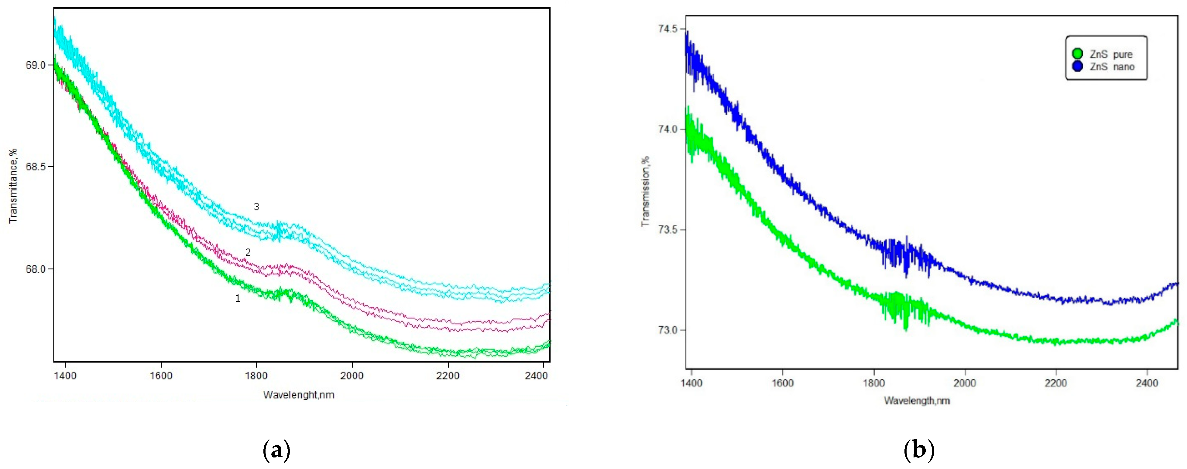
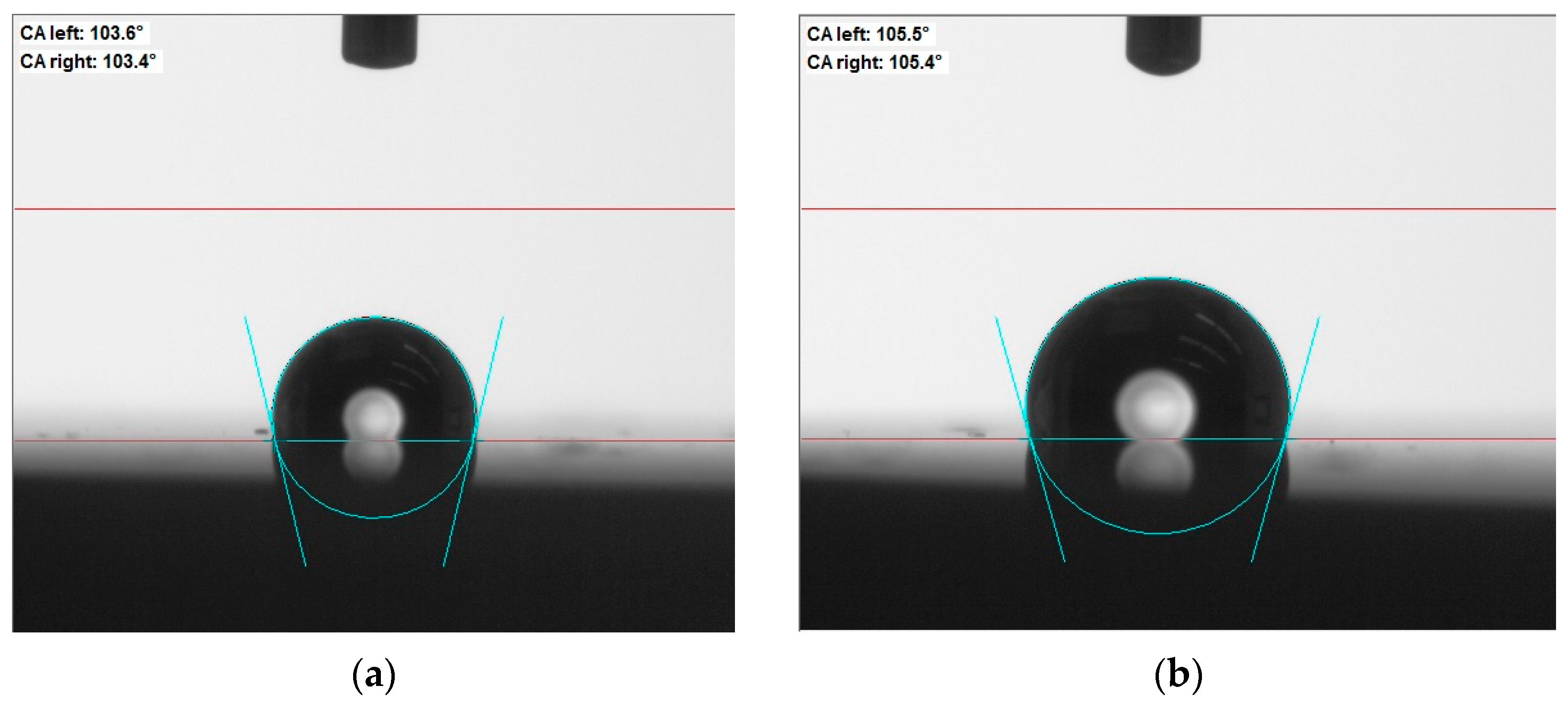
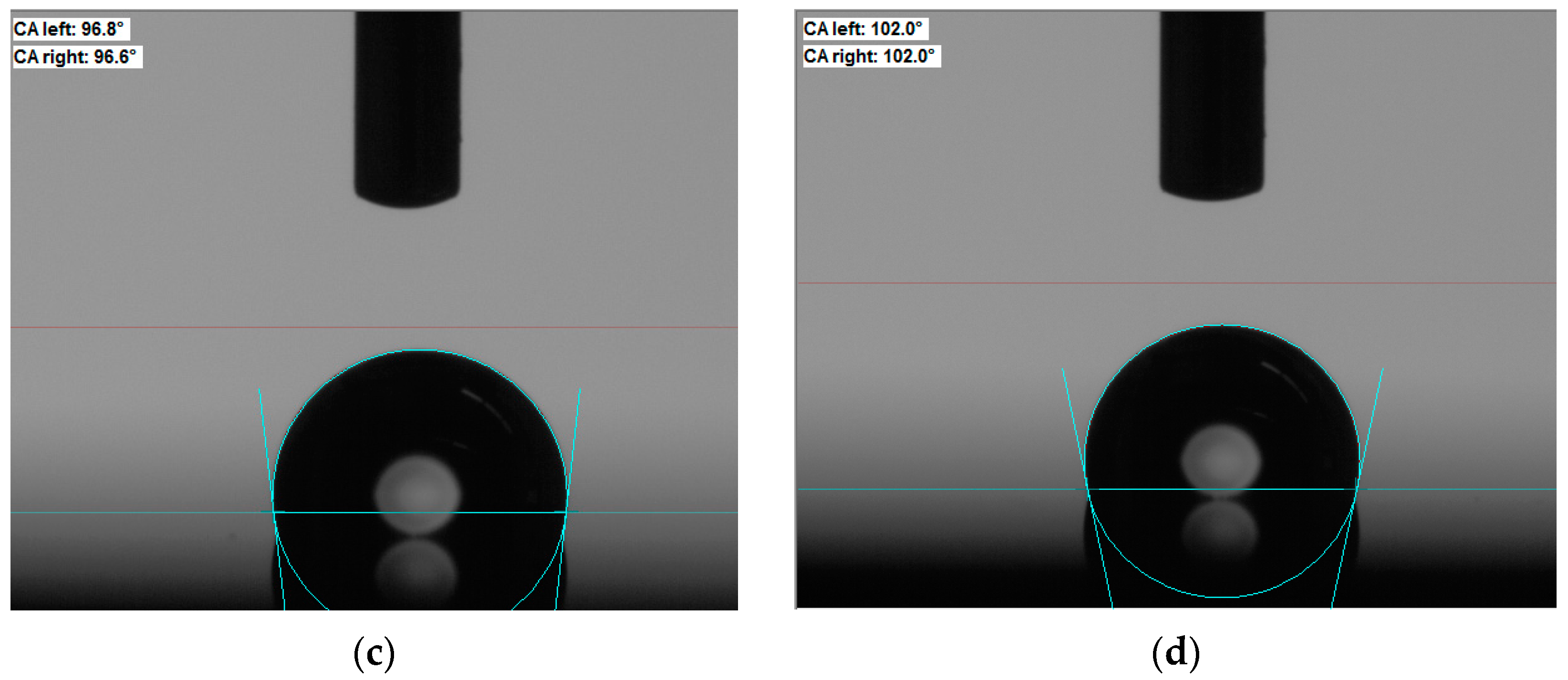
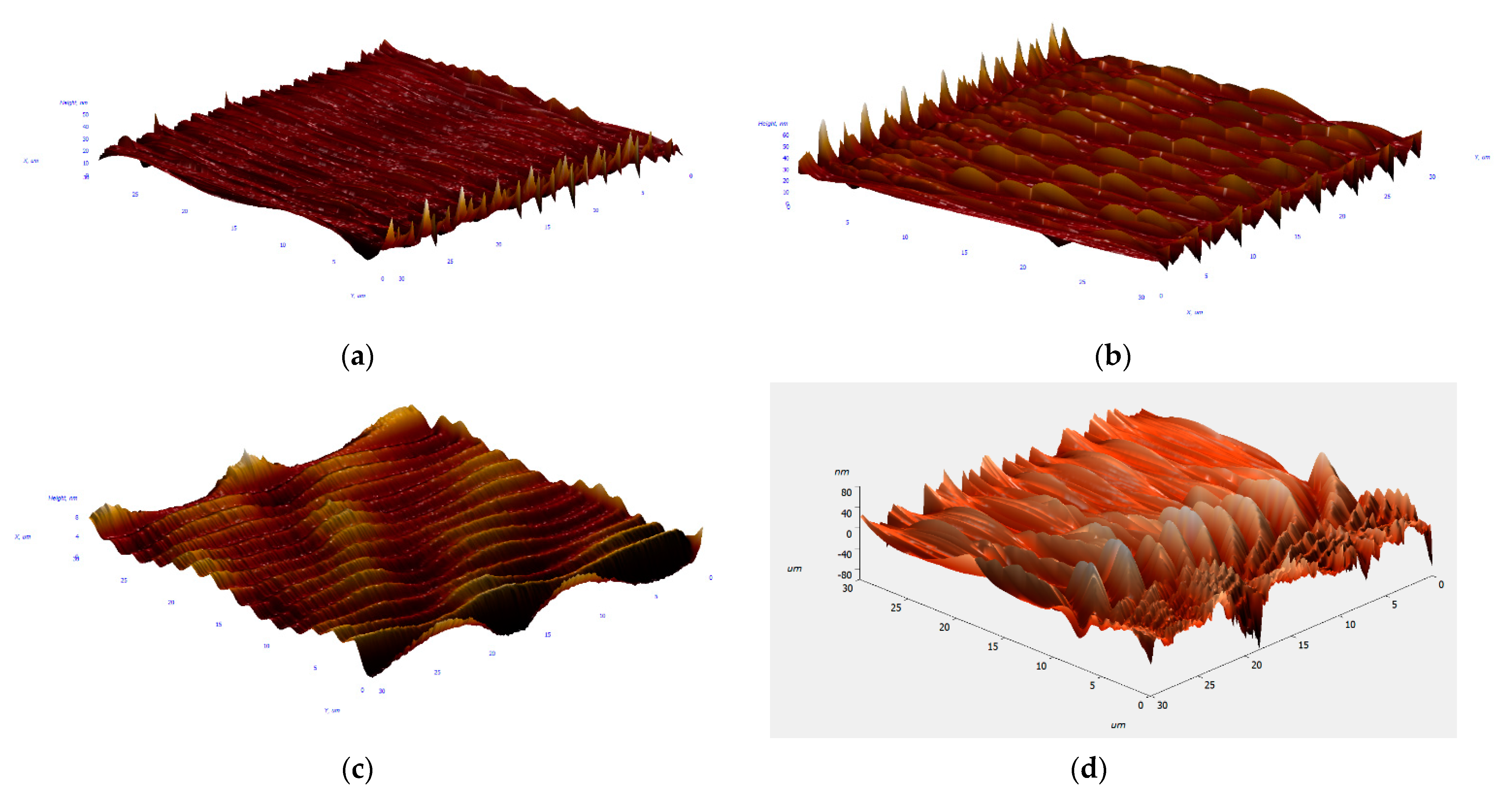
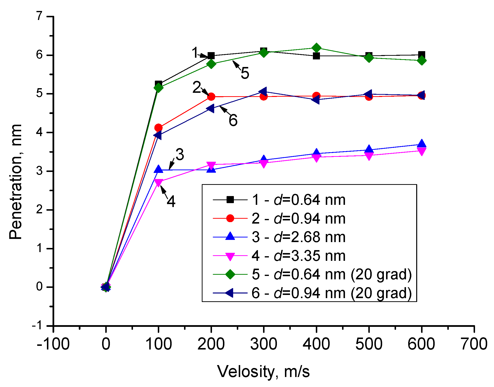
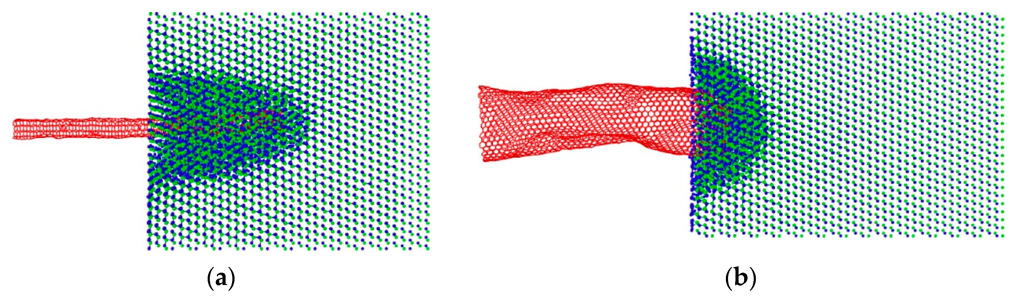
3. Results and Discussion

It is well known that the ZnSe and ZnS materials are the most promising key elements in the optical industry. ZnSe is used in X-ray detectors, in the development of the cores for the optical fibers, in the IR-laser techniques for windows of the CO2 lasers, etc. ZnS is used as a suitable material for the phosphors and for the semiconductor laser technology, etc. The LOD procedure indicates some advantage of the modified properties of such materials. Why? It is connected with the fact that the refractive index of the CNTs is so small and close to 1.1, but the Young modulus is so large and it is placed in the range of some teraPascales. Thus, the Fresnel losses can be decreased, the transparency can be increased, and the mechanical parameters can be improved.
It should be noticed that in order to study the structuration process influence on the physical and the chemical characteristics of the ZnSe and ZnS materials, the substrates with the polished surfaces have been used. The photos of the ZnSe and the ZnS samples studied are presented in Figure 2. It is worth noting that the ring is visible on the ZnS sample in Figure 2b, which was obtained when testing this sample for an abrasion to determine the mechanical strength, which will be discussed later.
Some change of the spectral characteristics of the ZnSe and the ZnS substrate in the range of 1,4 microns to 2,4 microns is shown in Figure 3. The image shows the influence of the CNTs structuration on the spectral parameters. Figure 3a (curve 1) presents the transmission of the pure ZnSe substrate on the wavelength range indicated above. Figure 3a (curve 2 and curve 3) shows the spectral characteristics after the treatment of the ZnSe surface from one side (Figure 3a; curve 2) and from both sides (Figure 3a; curve 3), respectively. The change of the spectral parameters for the pure ZnS and for the ZnS with one side treated by the CNTs is presented in Figure 3b. The green curve (lower one) shows the transmittance for the pure substrate; the blue curve (upper one) presents the transmittance for the ZnS covered with the CNTs. It is important that the surface treatment of samples with the CNTs can increase the transparency of both materials. It can be coincided with the fact that the CNTs refractive index is close to 1.1 [21,22], which is less than the refractive index of the ZnSe or ZnS materials; thus, the Fresnel losses can be decreased dramatically, which can predict the increase in the transparency.
The mechanical properties of the studied materials were investigated by two methods. Experiments were carried out to establish the microhardness of the nanostructured samples as well as to measure the comparative abrasion strength.
The microhardness improvement can be shown in the data presented in Table 1 for the ZnSe and ZnS structures. It was found that an implantation could increase the microhardness of the material up to 5% and 6.7%, respectively. Thus, the same tendency of the microhardness increasing via the CNTs covering by the LOD technique has been obtained for the ZnS and ZnSe substrates.
Moreover, the surface mechanical hardness (abrasive strength) for the ZnS and ZnSe materials has been established. The data are shown in Table 2. It should be noticed that the abrasion strength was compared with the abrasion of the glass K8 (crown glass), on which, with an indenter of 100 g, 3000 revolutions can be reached until a distinct ring appears. That is, with such a standard, namely crown glass K8, zero strength of the glass is achieved. Analyzing the data from Table 2, one can testify that the tendency to increase not only the microhardness but also the surface strength can be found for the ZnS and ZnSe materials with good advantage.
It is worth paying attention to the fact that different methods for determining the mechanical strength for the semiconductor materials based on the ZnS and ZnSe systems are not always the same for both. Different methods are more preferable for each of the materials. However, the general tendency of the mechanical strength increasing is maintained always and consistently.
Furthermore, for the ZnS and ZnSe materials, the wetting angle before and after the CNTs deposition has been established. The data of the wetting angle change are shown in Figure 4. When evaluating the averaging by the wetting angle, a sample was taken from the measurements of a batch of samples in the amount of 10 pieces.
One can see the slight change of the wetting angle for the ZnS (Figure 4a,b) and a better increase in the wetting angle for the ZnSe structure after its structuration by the CNTs (Figure 4c,d).
In addition, in order to support the matrix ZnS and ZnSe materials’ relief, modification of the AFM images have been made. The data are shown in Figure 5. One can see that the surface relief shown for the pure ZnS and ZnSe materials (Figure 5a,c) is absolutely different from the one that presented for the nanostructured surfaces (Figure 5b,d). Moreover, since the CNTs can be considered as donor–acceptor systems, the formation of the globules at the structured surfaces can be found.
Figure 6 shows the results of the MD simulations carried out. We calculated the dependence of the penetration depth of the CNT into the ZnS surface on the CNT diameter and its velocity and an inclination angle. The nanotube diameter was varied from 0.64 to 3.35 nm.
It can be seen that the CNT speed and their diameter as well as the angle of inclination on the substrate affects the final values of the penetration depth of the nanoobject into the ZnS surface. The qualitative representation of the process of the penetration of the CNTs with diameters of 0.64 nm (Figure 7a) and 2.68 nm (Figure 7b) into the ZnS surface layers with an initial velocity of 100 m/s is shown. It was found that the CNT with the smaller diameter penetrates more deeply than the CNTs with the wider diameter at the same initial velocity, which reflects its higher stiffness [37]. Figure 6 shows the process at the CNTs speed of 100 m/s.
We can plan to make the analogous simulation for the ZnSe materials and will show the results in the future publications.
Thus, the experimental results partially can be added by this simulation; it supports the fact of the effective application of the LOD technique in order to improve the basic properties of such materials with good advantage.

4. Conclusions

Analyzing the obtained and discussed data, the following conclusions should be drawn.
We have compared the properties of pure ZnS and ZnSe materials with those obtained after the modification procedure by the LOD method.
Structuration of the inorganic semiconducting surfaces (based on ZnS and ZnSe) by the CNTs shows the promising way of the surface modification with the aim of their transparency increase. The stronger increasing was observed in the case of treating both sides of the ZnS and ZnSe surfaces. This is due to the low refractive index of the CNTs, which allows reducing the loss of the reflection along the Fresnel law. The structuration of the ZnS and ZnSe surfaces shows the slight increase in the microhardness and the wetting angle. It can be connected with the large value of the Young’s module of the CNTs. The formation of the possible link between the carbon atoms and the surface materials permits increasing the hardness of the matrix materials as well. The laser-oriented deposition method can be applied with good advantage in order to improve the properties of the semiconductor materials. The obtained experimental results are partially supported by the molecular dynamic simulations.
It should be noted that all results are repeatedly checked with a multiplicity of the checks once a month. The error is plus or minus 0.5% and less. Moreover, all results of the modified ZnS and ZnSe have testified better data than shown, for example, in the classical books [38,39] for the pure materials.
Established data can show the promising route of the modification of the semiconductors surface with the purpose to form the structured materials with the desired optical properties which make them suitable for the applications as elements of optoelectronics, solar energy, gas storage systems, information technology, displays, and biomedicine. The knowledge accumulated can be used in the education process and for the practices as well.
For the future study, it will be useful to obtain and present the electronic microscopy images; it will be considered for the ZnS and ZnSe structures as well as other semiconducting materials.

Author Contributions

Conceptualization, formal analysis, writing—review and editing N.K.; investigation, A.T.; methodology, software D.K. and B.V. All authors have read and agreed to the published version of the manuscript.

Funding

The calculations were performed using the resources provided by the HybriLIT heterogeneous computing platform of the Joint Institute for Nuclear Research and supercomputer cluster provided by the Materials Modelling and Development Laboratory at NUST “MISIS” (supported via the grant from the Ministry of Education and Science of the Russian Federation No. 14.Y26.31.0005).

Institutional Review Board Statement

This work was carried out as an initiative. Consequently, it did not require any approval and conclusion from the Institute.

Informed Consent Statement

Consent to work; of course, it was obtained from all participants in this study.

Data Availability Statement

Using these primary materials of the article, as well as taking into account earlier developments on other materials, a patent will be created, as well as a message will be published in the media, for example, at LETI University, since the results are useful for teaching students.

Acknowledgments

The authors would like to thank their colleagues from Vavilov State Optical Institute, “LETI” University and Nuclear Physics Institute for the helpful discussions at the scientific seminars. Moreover, we would like to acknowledge our colleagues from Moscow Institutes for the on-line discussions.

Conflicts of Interest

The authors declare no conflict of interest.

References

  1. Barbagiovanni, E.G.; Lockwood, D.J.; Simpson, P.J.; Goncharova, L.V. Quantum confinement in Si and Ge nanostructures: Theory and experiment. Appl. Phys. Rev. 2014, 1, 011302. [Google Scholar] [CrossRef] [Green Version]
  2. Gautier, G.; Leduc, P. Porous silicon for electrical isolation in radio frequency devices: A review. Appl. Phys. Rev. 2014, 1, 011101. [Google Scholar] [CrossRef]
  3. Yang, D. Handbook of Photovoltaic Silicon; Springer: Berlin/Heidelberg, Germany, 2019; p. 967. ISBN 978-3-662-56473-8. [Google Scholar]
  4. Van Stryland, E.W.; Wu, Y.Y.; Hagan, D.J.; Soileau, M.J.; Mansour, K. Optical limiting with semiconductors. J. Opt. Soc. Am. B 1988, 5, 1980–1988. [Google Scholar] [CrossRef] [Green Version]
  5. Sandeep, A.; Saleem, K.; Parveen, L.; Ishan, G.; Suresh, K. Electrical properties of electrodeposited zinc selenide (ZnSe) nanowires. J. Mater. Sci. Mater. Electron. 2014, 25, 4150–4155. [Google Scholar] [CrossRef]
  6. Xu, S.; Qi, X.; Xu, X.; Wang, X.; Yang, Z.; Zhang, S.; Lin, T.; He, P. Effects of electroless nickel plating method for low temperature joining ZnS ceramics. J. Mater. Sci. Mater. Electron. 2019, 30, 15236–15249. [Google Scholar] [CrossRef]
  7. Pushkin, A.V.; Migal, E.A.; Tokita, S.; Korostelin, Y.V.; Potemkin, F.V. Femtosecond graphene mode-locked Fe: ZnSe laser at 4.4 μm. Opt. Lett. 2020, 45, 738–741. [Google Scholar] [CrossRef]
  8. Chan, L.; DeCuir, E.A.; Fu, R.; Morse, D.E.; Gordon, M.J. Biomimetic nanostructures in ZnS and ZnSe provide broadband anti-reflectivity. J. Opt. 2017, 19, 114007. [Google Scholar] [CrossRef]
  9. Dmitruk, I.; Berezovska, N.; Degoda, V.; Hrabovskyi, Y.; Kolodka, R.; Podust, G.; Stanovyi, O.; Blonskyi, I. Luminescence of Femtosecond Laser-Processed ZnSe Crystal. J. Nanomater. 2021, 2021, 6683040. [Google Scholar] [CrossRef]
  10. Cao, J.; Jiang, Z.J. Thickness-dependent Shell Homogeneity of ZnSe/CdSe Core/Shell Nanocrystals and Their Spectroscopic and Electron- and Hole-transfer Dynamics Properties. J. Phys. Chem. C 2020, 124, 12049–12064. [Google Scholar] [CrossRef]
  11. Kushwaha, K.K.; Kumari, S.; Mahobia, S.K.; Tiwary, S.K.; Sinha, B.K.; Ramrakhiani, M. Synthesis and Characterization of ZnSe/CdSe/ZnS Nano-particles Embedded in Polymer Matrix: A Review. Int. J. Compos. Const. Mater. 2018, 4, 28–33. [Google Scholar]
  12. Xiao, Y.; Deng, G.; Feng, G.; Ning, S.; Wang, S.; Chen, X.; Yang, H.; Zhou, S. Femtosecond laser induced nano-meter size surface structures on ZnSe film. AIP Adv. 2019, 9, 015106. [Google Scholar] [CrossRef] [Green Version]
  13. Lin, Z.Q.; Wang, G.G.; Li, L.H.; Wang, H.; Li, L.H.; Wang, H.; Tian, J.L.; Zhang, H.Y.; Han, J.C. Preparation and protection of ZnS surface sub-wavelength structure for infrared window. Appl. Surf. Sci. 2019, 470, 395–404. [Google Scholar] [CrossRef]
  14. Igweoko, A.E.; Augustine, C.; Idenyi, N.E.; Okorie, B.A.; Anyaegbunam, F.N.C. Influence of processing conditions on the optical properties of chemically deposited zinc sulphide (ZnS) thin film. Mater. Res. Express 2018, 5, 036413. [Google Scholar] [CrossRef]
  15. Nabesaka, K.; Ishikawa, Y.; Hosokawa, Y.; Uraoka, Y. Photomechanical modification of ZnS microcrystal to enhance electroluminescence by ultrashort-pulse laser processing. Appl. Phys. Express 2017, 10, 021201. [Google Scholar] [CrossRef]
  16. Li, X.; Li, M.; Liu, H.; Guo, Y. Fabrication of an Anti-Reflective Microstructure on ZnS by Femtosecond Laser Bessel Beams. Molecules 2021, 26, 4278. [Google Scholar] [CrossRef]
  17. Kamanina, N.V. Using the operator Laplace method to estimate the response time of space-time light modulators. Tech. Phys. 1994, 39, 83–85. [Google Scholar]
  18. Kamanina, N.V.; Vasilenko, N.A. Influence of operating conditions and of interface properties on dynamic characteristics of liquid-crystal spatial light modulators. Opt. Quantum Electron. 1997, 29, 1–9. [Google Scholar] [CrossRef]
  19. Zhang, F.; Wang, H.; Wang, C.; Zhao, Y.; Duan, J. Direct femtosecond laser writing of inverted array for broadband antireflection in the far-infrared. Opt. Lasers Eng. 2020, 129, 106062. [Google Scholar] [CrossRef]
  20. Mensah, N.G.; Nkrumah, G.; Mensah, S.Y.; Allotey, F.K.A. Temperature dependence of the thermal conductivity in chiral carbon nanotubes. Phys. Lett. A 2004, 329, 369–378. [Google Scholar] [CrossRef]
  21. Robertson, J. Realistic applications of CNTs. Mater. Today 2004, 7, 46–52. [Google Scholar] [CrossRef]
  22. Namilae, S.; Chandra, N.; Shet, C. Mechanical behavior of functionalized nanotubes. Chem. Phys. Lett. 2004, 387, 247–252. [Google Scholar] [CrossRef]
  23. Fa, W.; Yang, X.; Chen, J.; Dong, J. Optical properties of the semiconductor carbon nanotube intramolecular junctions. Phys. Lett. 2004, A323, 122–131. [Google Scholar] [CrossRef]
  24. Taherpour, A.A.; Aghagolnezhad-Gerdroudbari, A.; Rafiei, S. Theoretical and quantitative structural relationship studies of reorganization energies of [SWCNT(5,5)-Armchair-CnH20] (n=20–310) nanostructures by neural network CFFBP method. Int. J. Electrochem. Sci. 2012, 7, 2468–2486. [Google Scholar]
  25. Kamanina, N.V.; Likhomanova, S.V.; Kuzhakov, P.V. Advantages of the Surface Structuration of KBr Materials for Spectrometry and Sensors. Sensors 2018, 18, 3013. [Google Scholar] [CrossRef] [PubMed] [Green Version]
  26. Kamanina, N.; Kuzhakov, P.; Kvashnin, D. Novel Perspective Coatings for the Optoelectronic Elements: Features of the Carbon Nanotubes to Modify the Surface Relief of BaF2 Materials. Coatings 2020, 10, 7066. [Google Scholar] [CrossRef]
  27. Kamanina, N.; Borodianskiy, K.; Kvashnin, D. Surface Heterostructure of Aluminum with Carbon Nanotubes Obtained by Laser-Oriented Deposition. Coatings 2021, 11, 674. [Google Scholar] [CrossRef]
  28. Kamanina, N.V.; Vasilyev, P.Y. Optical Coatings Based on CNTs for the Optical Devises and Nanoelectronics. R.U. Patent 2 355 001 C2, 10 May 2009. [Google Scholar]
  29. Kamanina, N.V.; Vasilyev, P.Y.; Studeonov, V.I. Optical Coating Based on Oriented in the Electric Field CNTs for the Optical Devises, Micro- and Nanoelectronics under the Conditions When the Interface: Solid Substrate-Coating Can Be Eliminated. R.U. Patent 2 405 177 C2, 27 November 2010. [Google Scholar]
  30. Kamanina, N.V.; Kuzhakov, P.V.; Vasilyev, P.Y. Protective Coating for Hygroscopic Optical Materials Based on Laser-Deposited Carbon Nanotubes for the Purpose of Optoelectronics and Medical Equipment. R.U. Patent 2013118962 A, 27 October 2014. [Google Scholar]
  31. Plimpton, S. Fast Parallel Algorithms for Short-Range Molecular Dynamics. J. Comput. Phys. 1995, 117, 1–19. [Google Scholar] [CrossRef] [Green Version]
  32. Tersoff, J. New Empirical Approach for the Structure and Energy of Covalent Systems. Phys. Rev. B 1988, 37, 6991–7000. [Google Scholar] [CrossRef]
  33. Benkabou, F.; Aourag, H.; Certier, M. Atomistic Study of Zinc-Blende CdS, CdSe, ZnS, and ZnSe from Molecular Dynamics. Mater. Chem. Phys. 2000, 66, 10–16. [Google Scholar] [CrossRef]
  34. Tersoff, J. Modeling Solid-State Chemistry: Interatomic Potentials for Multicomponent Systems. Phys. Rev. B 1989, 39, 5566–5568. [Google Scholar] [CrossRef]
  35. Nosé, S. A Unified Formulation of the Constant Temperature Molecular Dynamics Methods. J. Chem. Phys. 1984, 81, 511–519. [Google Scholar] [CrossRef] [Green Version]
  36. Hoover, W.G. Canonical Dynamics: Equilibrium Phase-Space Distributions. Phys. Rev. A 1985, 31, 1695–1697. [Google Scholar] [CrossRef] [PubMed] [Green Version]
  37. Shima, H. Buckling of Carbon Nanotubes: A State of the Art Review. Materials 2011, 5, 47–84. [Google Scholar] [CrossRef] [PubMed] [Green Version]
  38. Morozova, N.K.; Kuznetsov, V.A.; Ryzhikov, V.D.; Galstyan, V.G. Zinc Selenide: Preparation and Optical Properties; Fok, M.V., Ed.; Russian Academy of Sciences, A.V. Shubnikov Institute of Crystallography: St. Petersburg, Russia, 1992; 95p. [Google Scholar]
  39. Bovina, L.A.; Brodin, M.S.; Valakh, M.Y. Physics of Compounds AIIBVI; Georgobiani, A.N., Sheinkman, M.K., Eds.; Phys. Mat. Lit.: Nauka, Russia, 1986; 320p. [Google Scholar]
Figure 1. The scheme to show the LOD process used for the ZnS and ZnSe materials more clearly.
Carbon 07 00084 g001
Figure 2. Photos of the ZnSe (a) and ZnS (b) samples studied in the current research.
Carbon 07 00084 g002
Figure 3. The ZnSe (a) and ZnS (b) transmittance in the near-IR-range.
Carbon 07 00084 g003
Figure 4. The wetting angle for the ZnS surface, pure (a) and with CNTs treatment (b). The wetting angle for the ZnSe surface, pure (c) and with CNTs treatment (d).
Carbon 07 00084 g004aCarbon 07 00084 g004b
Figure 5. The AFM images of the pure (a) and the structured (b) ZnS surfaces; the AFM images of the pure (c) and structured (d) ZnSe surfaces.
Carbon 07 00084 g005
Figure 6. The dependence of the penetration depth of CNTs into ZnS surface on the CNT velocity and its diameter.
Carbon 07 00084 g006
Figure 7. The qualitative representation of the CNT penetration with the diameter of 0.64 nm (a) and 2.68 nm (b) into the ZnS surface.
Carbon 07 00084 g007
Table 1. The comparative data of the ZnSe and ZnS microhardness change, when an indentor was 20 g.
Material StudiedMiddle Value of the Microhardness, Pa × 109
Pure ZnSe0.1118
ZnSe structured with CNTs0.1175
Pure ZnS0.8589
ZnS structured with CNTs0.91675
Table 2. The comparative data of the ZnS and ZnSe surface hardness when an indentor was 100 g.
Material StudiedThe Number of Revolutions on the Abrasion Surface before the Appearance of a Distinct Ring
Pure ZnS100–120
ZnS structured with CNTs200–220
Pure ZnSe420
ZneS structured with CNTs600
Publisher’s Note: MDPI stays neutral with regard to jurisdictional claims in published maps and institutional affiliations.

