Article

Atomic Layer Deposition of Nanolayered Carbon Films

1
Department of Electrical Engineering and Computer Science, Alabama A&M University, Normal, AL 35762, USA
2
Center for Functional Nanomaterials, Brookhaven National Laboratory, Upton, NY 11973, USA
3
Materials Characterization Facility, Georgia Institute of Technology, Atlanta, GA 30332, USA
*
Author to whom correspondence should be addressed.
Submission received: 26 August 2021 / Revised: 23 September 2021 / Accepted: 24 September 2021 / Published: 27 September 2021

Abstract

:
In this paper, carbon thin films were grown using the plasma-enhanced atomic layer deposition (PE-ALD). Methane (CH4) was used as the carbon precursor to grow the carbon thin film. The grown film was analyzed by the high-resolution transmission electron micrograph (TEM), X-ray photoelectron spectroscopy (XPS) analysis, and Raman spectrum analysis. The analyses show that the PE-ALD-grown carbon film has an amorphous structure. It was found that the existence of defective sites (nanoscale holes or cracks) on the substrate of copper foil could facilitate the formation of nanolayered carbon films. The mechanism for the formation of nanolayered carbon film in the nanoscale holes was discussed. This finding could be used for the controlled growth of nanolayered carbon films or other two-dimensional nanomaterials while combining with modern nanopatterning techniques.

1. Introduction

Since the discovery of mechanically exfoliated graphene in 2004 [1], research on two-dimensional (2D) nanomaterials has grown exponentially due to their compelling physical, chemical, and electrical properties such as high current-carrying capacity, high mobility, and ballistic quantum transport [2,3,4,5,6,7,8,9,10,11,12,13,14,15]. Graphene, a single layer of carbon atoms bonded together in a hexagonal lattice, has a perfect 2D structure, while other 2D nanomaterials such as 2D boron nitride and transition metal dichalcogenide nanomaterials have 2D structures similar to graphene. The unique 2D structure with a lateral size of about 100 nm to a few micrometers and a thickness of only a single atom or few atoms confines electrons and holes to move in a 2D plane, resulting in a strong quantum effect, which produce novel physical, chemical, and electrical properties in the 2D nanomaterials and devices [16,17,18,19]. Their strong in-plane covalent bond and atomic thickness also make the 2D nanomaterials have excellent mechanical strength and flexibility [20,21]. Electrons and holes undergo ballistic transport on the sub-micrometer scale without collision in 2D nanomaterials and do not suffer from the scale limitations of current metal-oxide-semiconductor field-effect transistors (MOSFET); therefore, nanoelectronic devices built on 2D materials offer many benefits for further miniaturization in the device fabrication and the possibility to revolutionize the silicon-based semiconductor technology in the future [22,23,24,25,26,27,28], allowing for the Moore’s Law to continue on its path [29].
Current methods for the preparation of 2D nanomaterials are divided into the top-down method and the bottom-up method [17]. The top-down method relies on the exfoliation of thin layer 2D crystals from their parent layered bulk crystals using processes such as mechanical cleavage and mechanical force-assisted liquid exfoliation, while the bottom-up method is based on the chemical reactions such as chemical vapor deposition (CVD) growth and wet-chemical syntheses. The top-down method has numerous limitations for the application of device fabrication, while the bottom-up method is more promising and could grow 2D nanomaterials with desired compositions and crystal phases and enhanced physical, chemical, and electrical properties. The CVD method is the most popular and effective method for the large-scale synthesis of 2D nanomaterials [30,31,32,33,34,35].
Atomic layer deposition (ALD) is a special modification of conventional chemical vapor deposition (CVD) for growing thin films [36]. In conventional chemical vapor deposition (CVD), precursors are simultaneously supplied to a substrate, but in atomic layer deposition (ALD), the precursors are alternately exposed onto the substrate and subsequently purged for each precursor. One ALD cycle generally consists of two half-reactions, which are achieved by repeating four steps (the first precursor exposure and purging steps for the first half-reaction, and the second precursor exposure and purging steps for the second half-reaction) [37,38,39,40]. Plasma-enhanced atomic layer deposition (PE-ALD) is an extension of thermal ALD in which gas-phase plasma electron impact is substituted for thermal agitation, thereby achieving much lower substrate temperatures [41]. Sequential self-limiting surface reactions allow for precise thickness control, high conformality, and scalability to large surface areas, making ALD an ideal candidate for growing 2D nanomaterials.
In this research, we report the growth of carbon thin films using the plasma-enhanced atomic layer deposition (PE-ALD) and the finding that the existence of defective sites (nanoscale holes or cracks) on the substrate of copper foil could facilitate the formation of nanolayered carbon films. This finding could be used for the controlled growth of nanolayered carbon films or other two-dimensional nanomaterials while combining with modern nanopatterning techniques.

2. Experimental Details (Methods)

A plasma-enhanced atomic layer deposition system (ALD-150LX, Kurt J. Lesker Company, Frankfurt am Main, Germany) was used to grow the carbon film in this research [42]. Methane (CH4) was used as the precursor for the carbon source, and Ar/H2 were used for both plasma and purge gases during the deposition. The process chamber had a base pressure of 5 × 10⁻⁷ Torr. Carrier gas mass flow controllers (MFC), high-speed ALD valves, and shut-off valves were used to control the flow of carrier gas, precursor, and reactant gas into the process chamber. The inductively coupled remote plasma source was set at 1000 W to generate plasma and the substrate holder, which is electrically grounded was heated at 500 °C during the growth of carbon films. Two types of substrates were used for the growth of carbon films. One substrate was a 25 mm thick Cu foil (Alfa Aesar, Havrier, MA, USA, 99.8%), the other one was a 3-inch diameter <100> silicon wafer (n-type, with ~3 Ω cm resistivity from Virginia Semi-conductor, Inc., Fredericksburg, VA, USA) covered by a 100 nm thick copper (Cu) thin film. The Cu thin film was grown on the silicon substrate with e-beam evaporation using an e-beam/thermal evaporation system (PVD 75 from Kurt J. Lesker), and copper (Cu) slug (3.175 mm diameter × 3.175 mm length; 99.99% pure from Alfa Aesar) was used as the Cu source material. The Cu foil was dipped in buffered hydrofluoric acid (BHF) (Transene Company, Danvers, MA, USA) for 30 s to etch away any possible oxides such as copper oxide (CuO) on the surface before being transformed to the deposition chamber. The Cu-thin-film-covered silicon substrate was transformed to the deposition chamber right after the deposition of the Cu thin film on the silicon substrate. After being transferred onto the substrate holder, the Cu foil substrate was cleaned by H2 (65 sccm)/Ar (65 sccm) plasma gas at 1 kW for 10 min, immediately followed by the growth of the carbon film, while the Cu-thin-film-covered silicon substrate was cleaned by H2 (65 sccm)/Ar (65 sccm) plasma gas at 1 kW for 1 min. The total chamber pressure was about 1.2 Torr. The time for each pulse cycle during the growth of the carbon film was set as follows: 100 ms for CH4, 1000 ms for Ar purge, 6000 ms for H2 (65 sccm)/Ar (65 sccm) plasma, and 1000 ms for Ar purge. The carbon films were grown for 200 cycles.

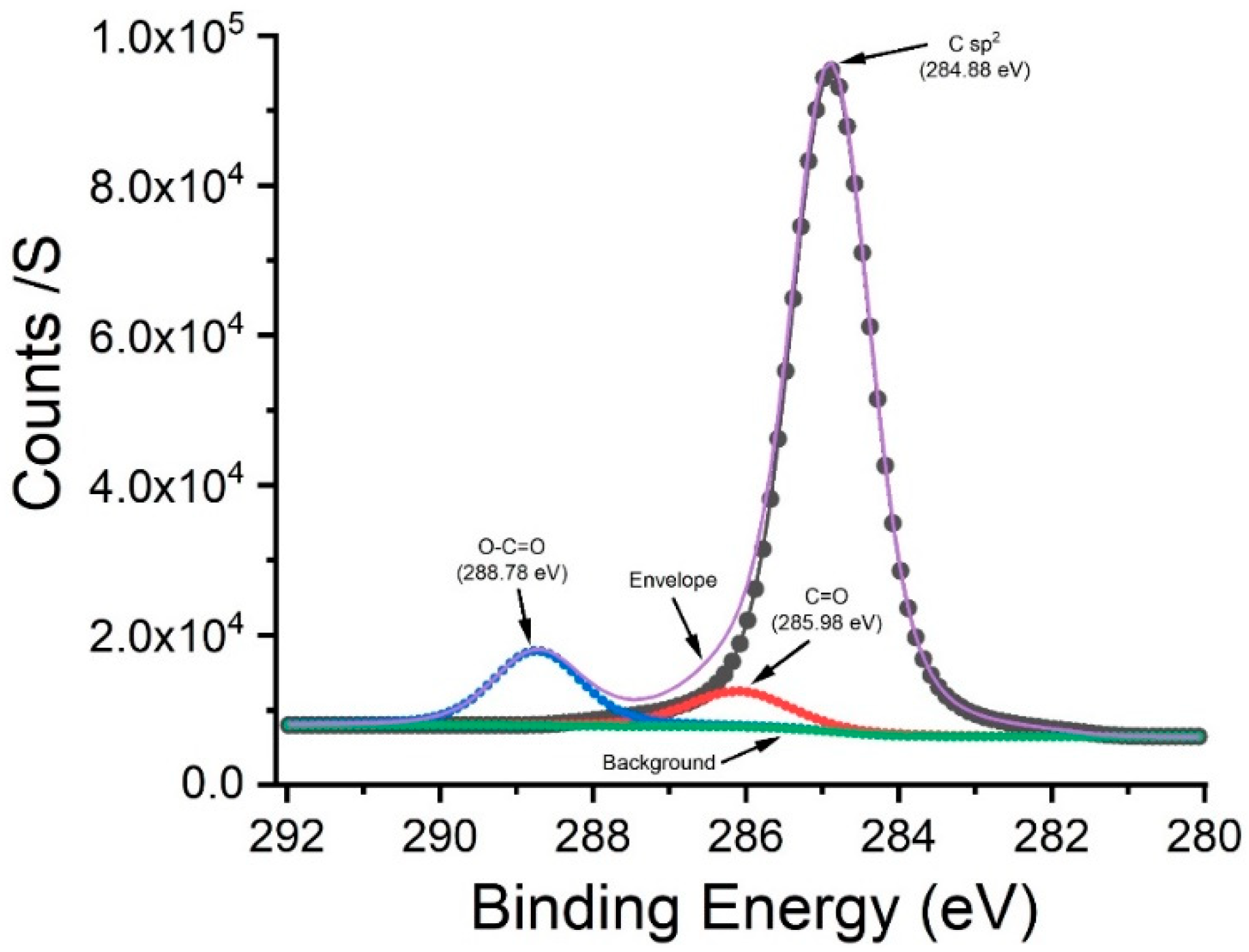
2.1. X-ray Photoelectron Spectroscopy (XPS) for Analysis of the Composition and Atomic Concentration of the Carbon Film

X-ray photoelectron spectroscopy (XPS) was performed using the Thermo K-alpha XPS system. The samples were cleaned with IPA and nitrogen gun before running on the XPS. Surface analysis by XPS was achieved by irradiating the sample with a monochromatic source of Al K Alpha X Rays (1.486 KeV). The tool was calibrated with Cu2p, Ag3d, and Au4f internal standards. Low-energy ionized Argon gas was used as a flood gun source for charge neutralization.

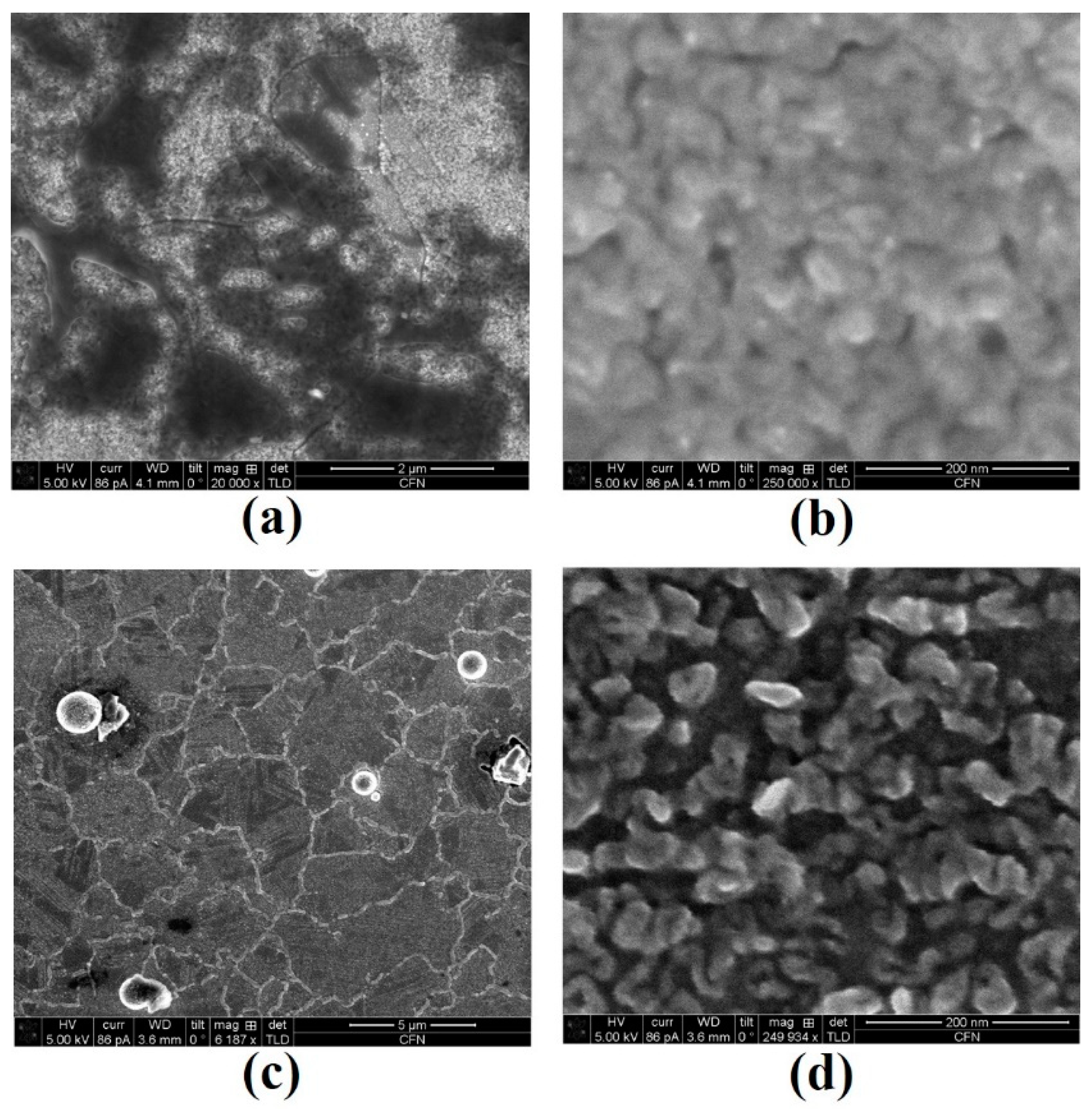
2.2. Scanning Electron Micrograph (SEM) for the Imaging and Analysis of the Surface Morphology of Carbon Films

A scanning electron microscope/focused ion beam (SEM/FIB) dual-beam system (Helios 600 from Thermo Fisher Scientific, Waltham, MA, USA) was used to image and analyze the surface of the grown carbon films.

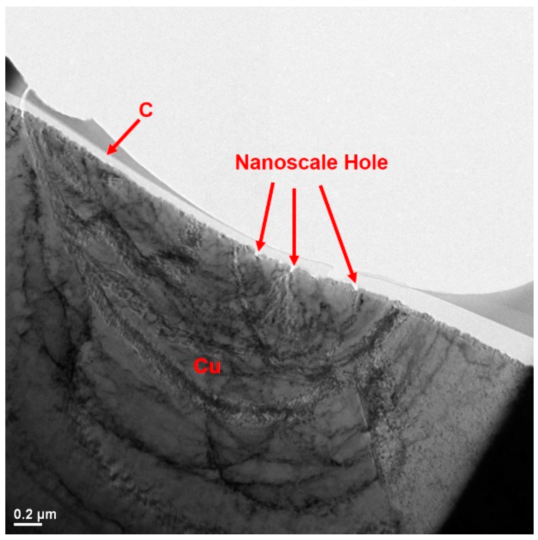
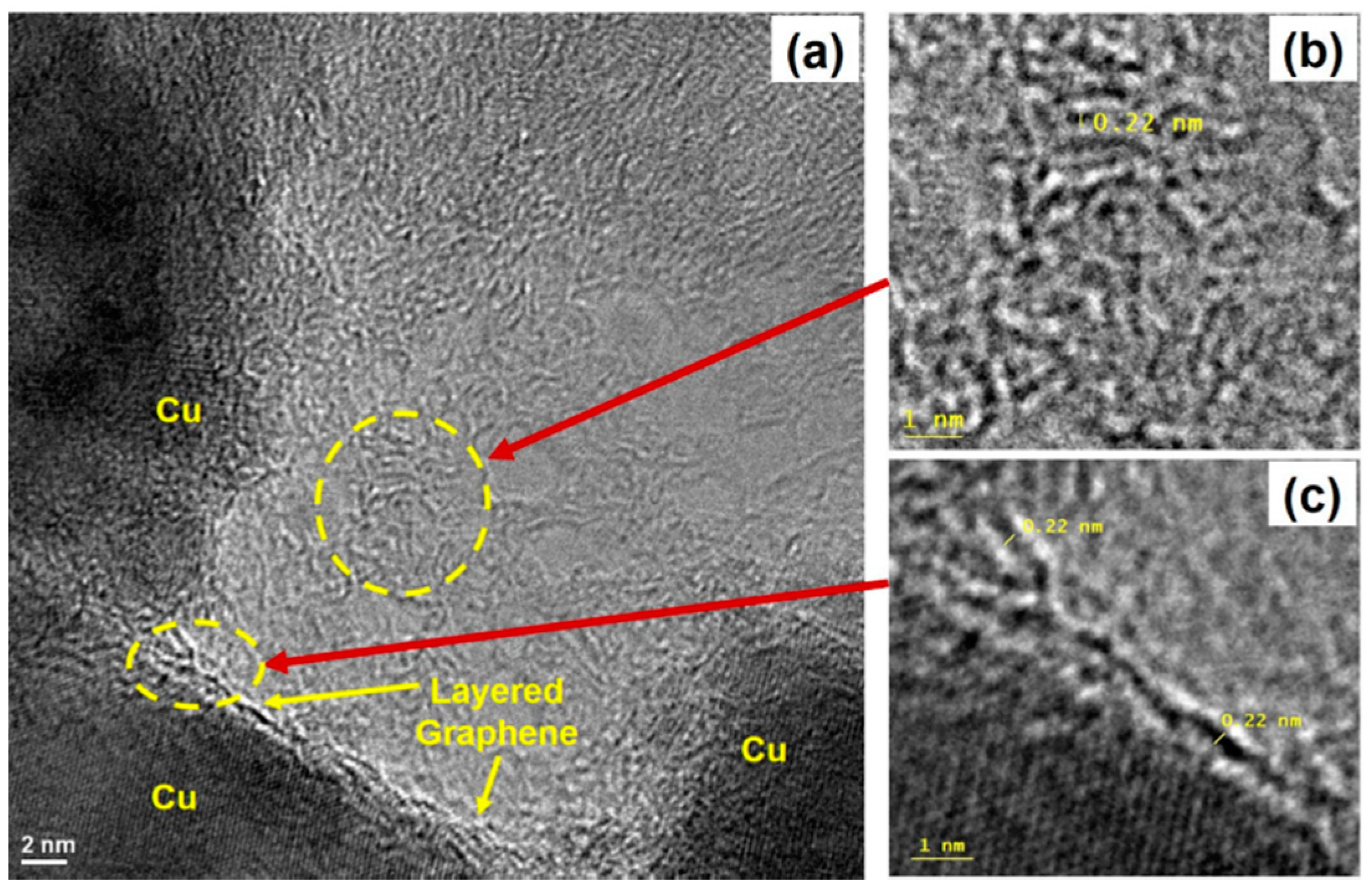
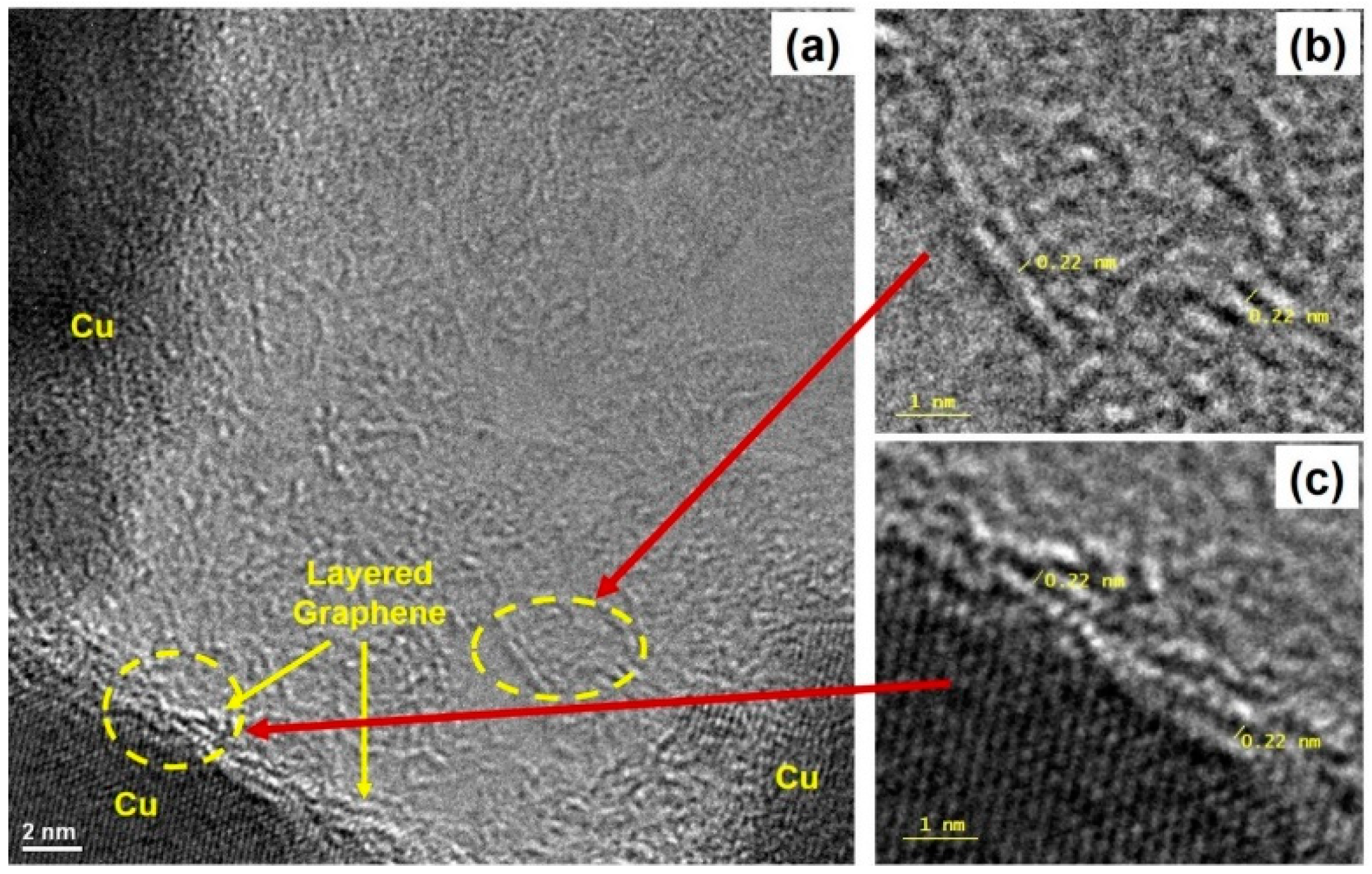
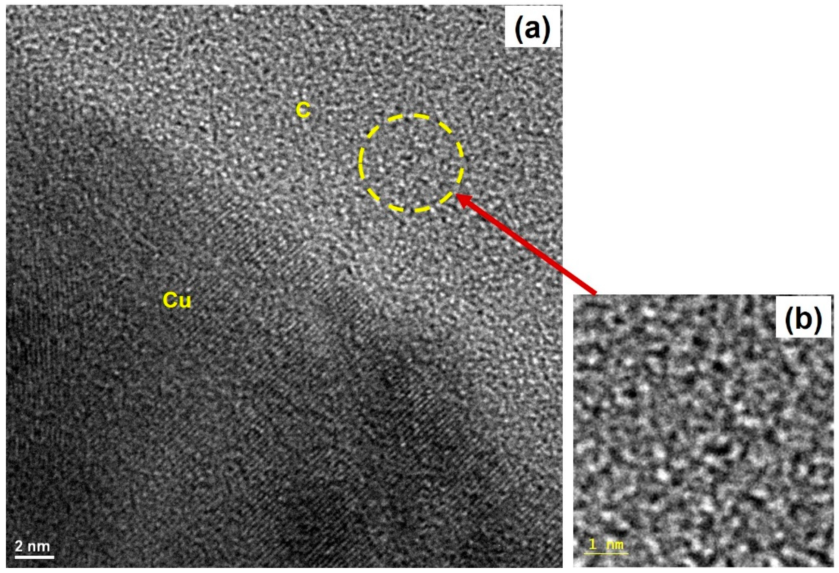
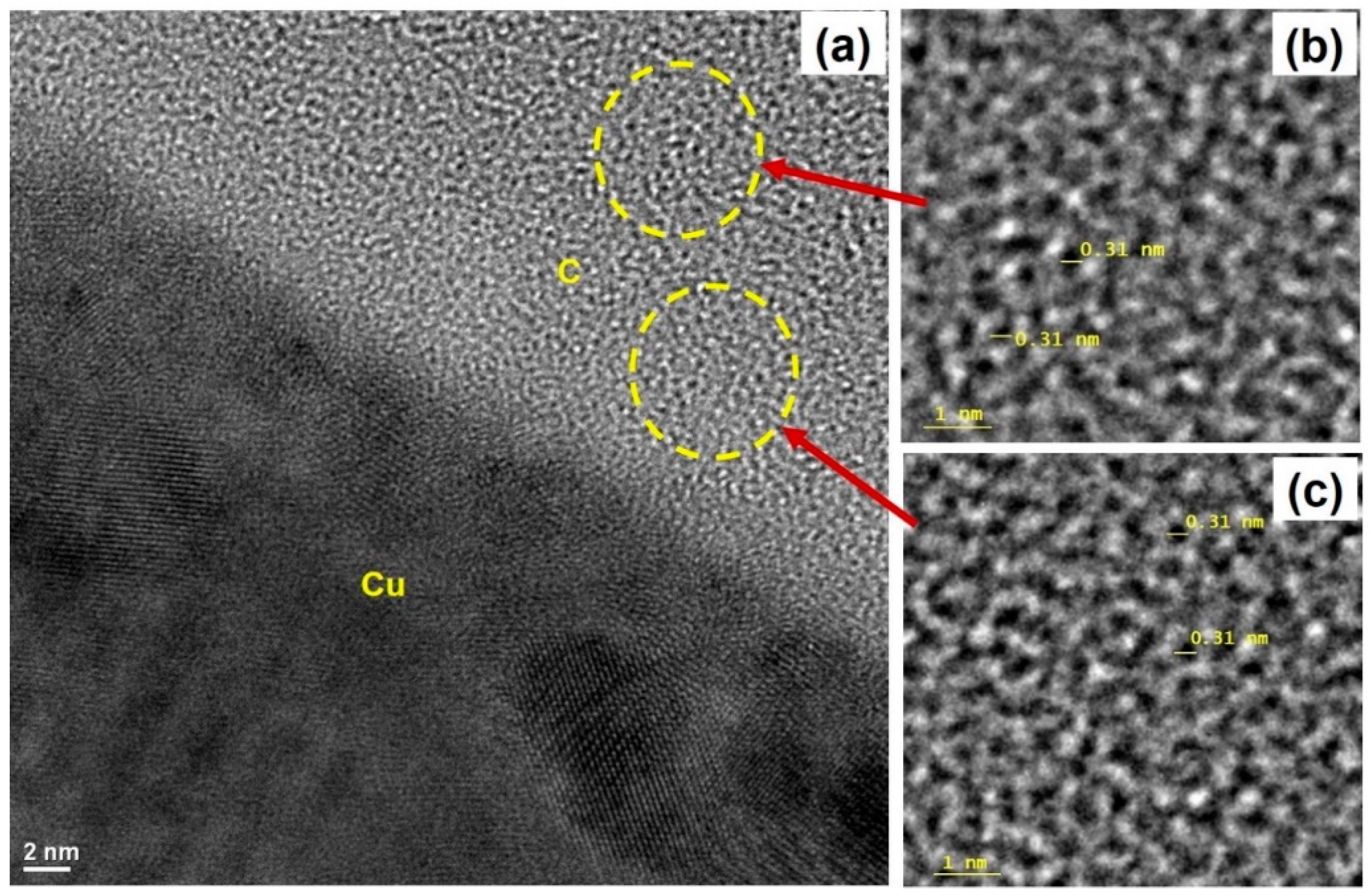
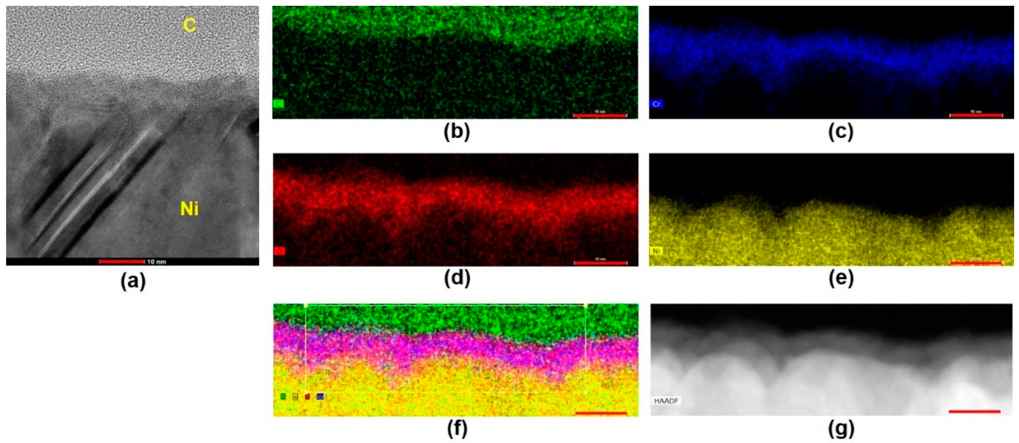
2.3. High-Resolution Tunneling Electron Micrograph (HRTEM) Imaging and Energy Dispersive Spectroscopy (EDS) Mapping of Carbon Films

To characterize the carbon film structure and composition in a transmission electron microscope (TEM), electron transparent cross-sectional samples (lamella) of the grown carbon films were extracted using the standard in situ lift-out method [43] in a scanning electron microscope/focused ion beam (SEM/FIB) dual-beam system (Helios 600 from Thermo Fisher Scientific). High-resolution images were acquired with 200 keV e-beam energy in a high-resolution analytical transmission electron microscope (JEOL JEM-2100F, Showa, Tokyo, Japan). High-resolution images and energy dispersive spectroscopy (EDS) maps were acquired with 200 keV e-beam energy in a scanning TEM (STEM)/TEM (Talos F200X from Thermo Fisher Scientific) equipped with a four-quadrant 0.9 sr X-ray detector.

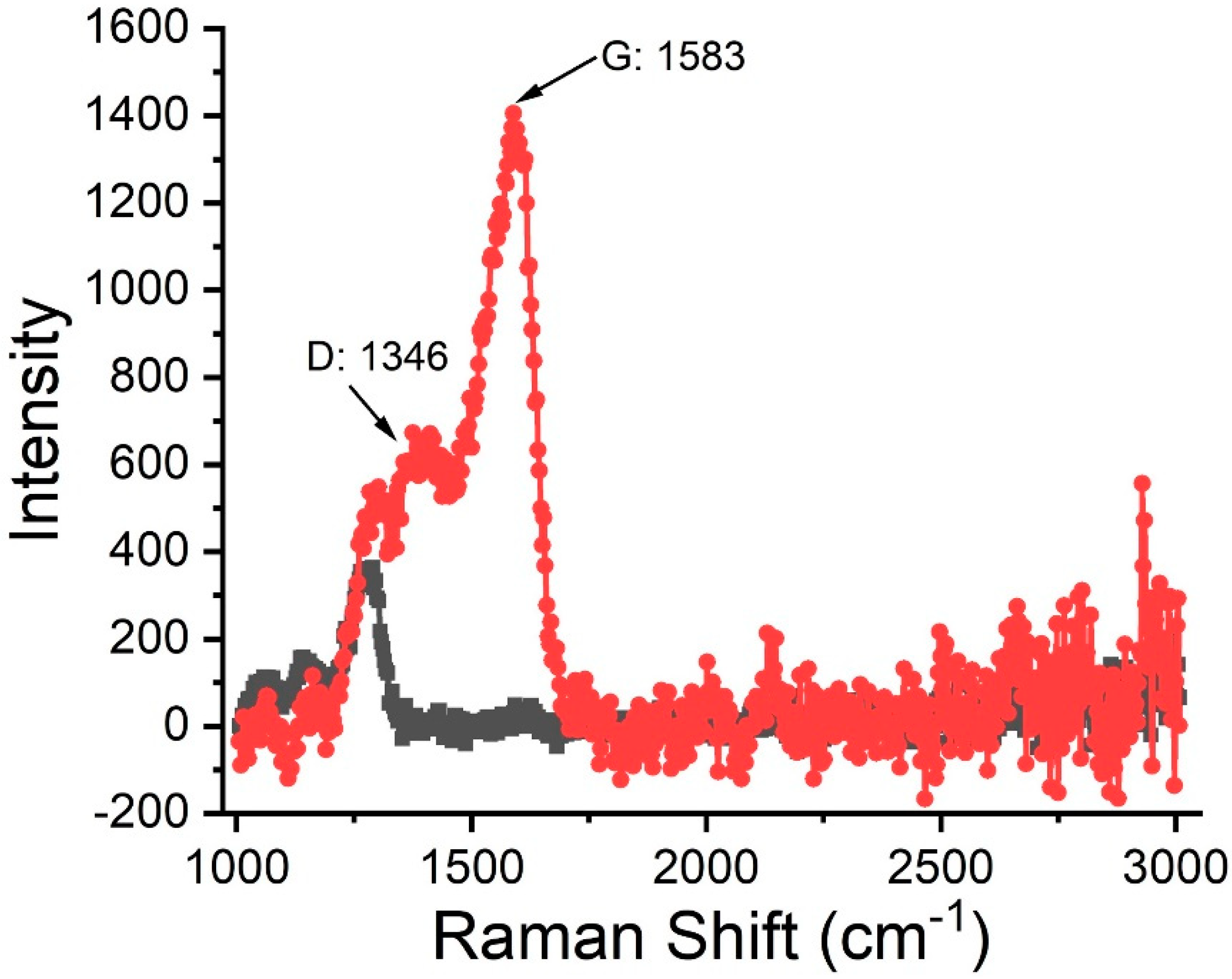
2.4. Raman Spectroscopy Analysis of Carbon Films

Raman spectroscopy was obtained using a Renishaw Invia Qontor Confocal Raman Microscope. A 488 nm optically pumped semiconductor laser (OPSL, Lagos, Nigeria) was used. An automated 2D Raman mapping was performed to scan the sample surface for the analysis of Raman shift. A continuous overlay of Raman over optical image (white light) map is achieved using a small step size of 1 micron and a 2-micron laser spot size.

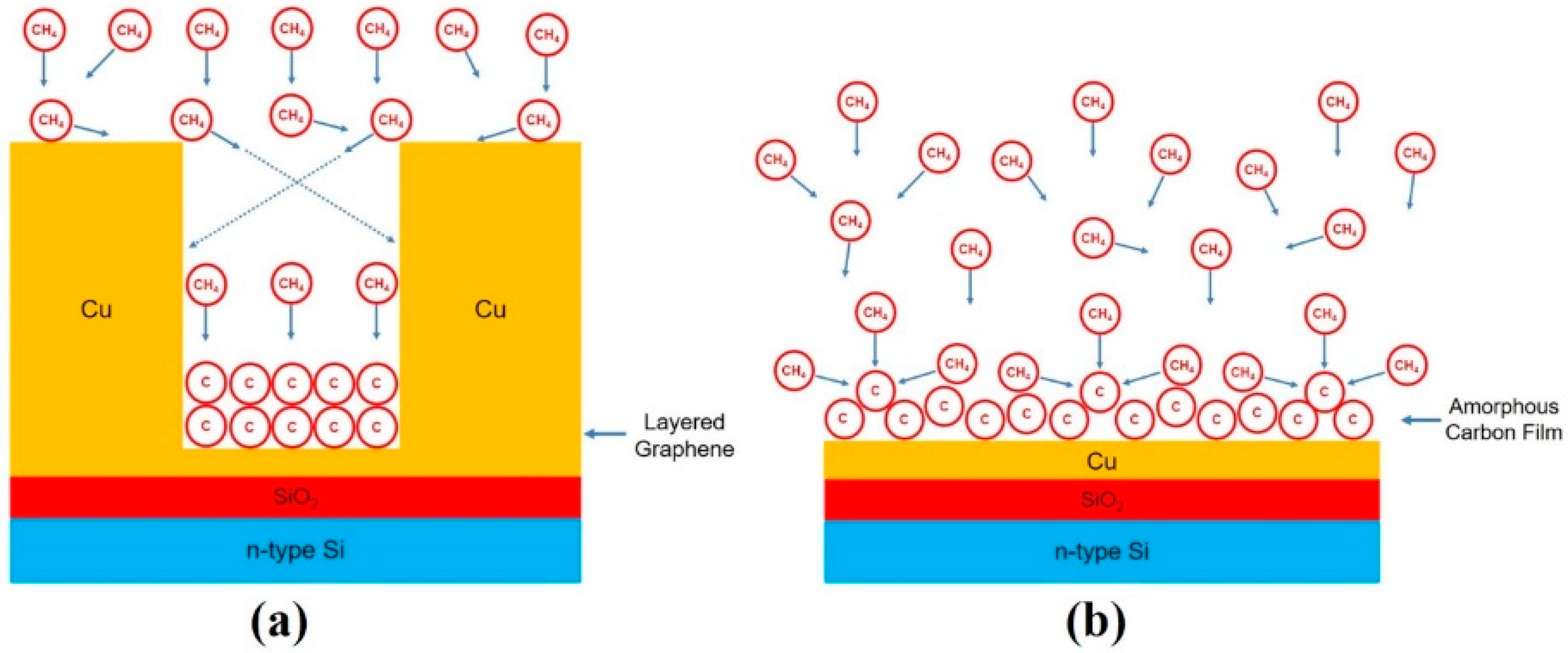
3. Results and Discussion

Table A1 summarizes the compositions and atomic concentrations, which were obtained by the XPS analysis for the carbon film grown by the remote plasma-enhanced atomic layer deposition. The carbon film has atomic concentrations of 72% C, 20% O, 3% Cu, and 5% others (F, Ca, and Cl). Figure A1 shows the high-resolution XPS scan of the C sp2 in the carbon thin film, indicating that the PE-ALD-grown carbon film is an amorphous film. The C 1s core-level XPS peaks of highly ordered graphene layers exhibit asymmetric shapes with higher intensity at higher binding energy from the center position of the peak due to the high electron densities at Fermi levels [44,45,46,47,48]. Figure A2a is an SEM image of the surface of the carbon film grown on the copper (Cu) foil substrate, and Figure A2b is the SEM image of an enlarged view of the carbon film, while Figure A2c is an SEM image of the surface of the carbon film grown on the Cu-thin-film covered silicon substrate, and Figure A2d is the SEM image of an enlarged view of the carbon film. Figure A3 is the cross-sectional TEM image of the copper (Cu) foil substrate with a ~50 nm thick carbon thin film grown on it, showing a rough substrate surface with some nanoscale holes or nanoscale cracks on the surface. After the further cross-sectional analysis of the grown carbon thin-film sample by high-resolution transmission electron micrograph (TEM), it was found that the film grown in the nanoscale holes had the structure of nanolayered graphene, while the film grown on the hole-free flat smooth surface was an amorphous carbon film without any nanolayered structure. Figure A4a is the high-resolution cross-sectional TEM image of the carbon thin film grown in a nanoscale hole, clearly showing some nanolayered structures; Figure A4b is an enlarged view of the film inside the hole, showing nanolayered structures, while Figure A4c is an enlarged view of the film on the bottom surface of the Cu nanohole, showing nanolayered carbon films, which have a difference of about 0.22 nm between layers [49]. Figure A5a–c shows the high-resolution cross-sectional TEM images of the carbon thin film grown in another Cu nanoscale hole, presenting similar nanolayered structures in Figure A4a–c. Figure A6a is the high-resolution cross-sectional TEM image of the carbon film grown on a hole-free flat smooth surface of the same Cu foil substrate, showing a homogenous amorphous carbon film without any nanolayered structures on the interface or anywhere else; Figure A6b is an enlarged view of the film. Figure A7a is the high-resolution cross-sectional TEM image of the carbon film grown on the Cu-thin-film-covered silicon substrate, showing a similar amorphous structure as Figure A6a, without any nanolayered structures; Figure A7b,c shows the enlarged views of the film. The TEM image of the carbon film grown on the Cu thin film further confirms that the carbon film grown on a hole-free surface of copper is an amorphous film in the experimental conditions.
The carbon film grown on the chromium (Cr)/nickel (Ni) film was also investigated. A Ni film was grown on the silicon wafer using the e-beam evaporation, followed by a thin Cr layer. The carbon film was then grown using the PE-ALD with the same experimental condition for the growth of the carbon films on copper foil and a copper-covered silicon substrate. Figure A8a shows the high-resolution cross-sectional TEM image of the carbon film on the Cr/Ni film. The film is an amorphous carbon film and is similar to those in Figure A6 and Figure A7, without any nanolayered structures on the interface or anywhere else. Figure A8b–f summarizes the energy dispersive spectroscopy (EDS) elemental map analysis in the interface region of the sample: Figure A8b is the color-coded EDS elemental map of carbon (C), where the green color represents the C K-alpha X-ray signal; Figure A8c is the EDS elemental map of Cr (blue); Figure A8d is the EDS elemental map of O (red), which overlaps with the Cr in Figure A8c, indicating that the Cr layer was oxidized; Figure A8e is the EDS elemental map of Ni (yellow); Figure A8f is the color-coded EDS elemental map of C, Cr, O, Ni combined together. Figure A8g shows the high-angle annular dark-field (HAADF) STEM micrograph of the same region mapped in Figure A8f, clearly showing the high atomic number (Z) Cr and Ni layers.
Figure A9 shows the two typical Raman spectra measured from the carbon film grown on the Cu foil substrate, where the red line has the characteristic D and G peaks, while the black line does not have the D and G peaks. The Raman analysis was performed with the 2D mapping measurement on the surface of carbon film, where the areas for the measurement were selected randomly. The analysis from 100 measurement scans shows that about 60% of the measurements have a Raman spectrum similar to the red line, while about 40% have a Raman spectrum similar to the black line. The 2D mapping measurement did not find the 2D peaks, indicating that the PE-ALD-grown carbon film is an amorphous film [50,51,52].
Mechanism of chemical vapor deposition (CVD) or atomic layer deposition (ALD) includes diffusion of gas toward the substrate surface, absorption to the surface, reaction, desorption, and diffusion of by-product. The possible reason why the nanolayered carbon film was formed in the nanoscale Cu hole is that the hole selected the neutral species (methane molecules (CH4)) or ionic species (CH3) with a certain moving direction and only allowed the species (CH4 or CH3) that had a parallel or close parallel moving direction to the wall of nanohole to enter the hole, which facilitated the nanolayered structure. Figure A10a,b shows the possible mechanism for the growth of nanolayered carbon film in the nanoscale Cu hole and the growth of homogeneous amorphous carbon film on a flat smooth Cu surface, respectively. The nanoscale hole in Figure A10a functions similar to a filter that blocks most methane molecules (CH4) or other ionized groups such as methyl group (CH3) with random moving directions, and only those with a moving direction parallel or close parallel to the wall of nanohole can enter the hole. The species with the same moving direction arrive on the Cu interface in order, facilitating the formation of the nanolayers while the hole-free flat Cu surface in Figure A10b is subjected to methane molecules (CH4) or ionized groups from every direction simultaneously, resulting in a uniform amorphous carbon film without forming any nanolayered structure. Researchers found that electric fields could be manipulated to grow nanostructured carbon films [53,54] or graphene [55]. The electric field made the ionic species flow in a certain direction, and the ionic species moving in order facilitated the growth of the nanostructured carbon films or graphene. Nanoscale holes could be precisely patterned and fabricated with the hole diameter, down to a few nanometers, using the nanofabrication patterning techniques [56]; further research on the growth of carbon films on a substrate with uniform-patterned nanoscale holes may confirm the mechanism or suggest a different explanation about the phenomenon that the formation of the amorphous carbon layer could be varied by the existence of defective sites (nanoscale holes or cracks) on the substrate.

4. Summary

In summary, carbon thin films were grown using the plasma-enhanced atomic layer deposition (PE-ALD). The carbon film was analyzed using the high-resolution transmission electron micrograph (TEM), X-ray photoelectron spectroscopy (XPS) analysis, and Raman spectrum analysis, indicating that the PE-ALD-grown carbon film has an amorphous structure. The existence of defective sites (nanoscale holes or cracks) on the substrate was found to facilitate the formation of nanolayered carbon films in the plasma-enhanced atomic layer deposition of carbon films. This finding could be used for the controlled growth of nanolayered carbon films or other two-dimensional nanomaterials while combining with modern nanopatterning techniques.

Author Contributions

Z.X. designed the experiments, fabricated the materials, analyzed the data, and wrote the manuscript. K.K. performed the HRTEM experiment and contributed to analyzing the data and writing the manuscript. R.M. performed the Raman and XPS experiments and contributed to analyzing the data and writing the manuscript. All authors have read and agreed to the published version of the manuscript.

Funding

U.S. Department of Energy, Office of Basic Energy Sciences, under Contract No. DE-SC00112704; National Science Foundation under Grant No. CBET-1740687 and Grant No. ECCS-1542174; Department of Defense under Grant No. W911NF-16-1-0554.

Acknowledgments

Research carried out in part at the Center for Functional Nanomaterials, Brookhaven National Laboratory, which is supported by the U.S. Department of Energy, Office of Basic Energy Sciences, under Contract No. DE-SC00112704; XPS and Raman measurements were carried out at the IEN/IMAT Material Characterization Facility, in part at the Georgia Tech Institute for Electronics and Nanotechnology, a member of the National Nanotechnology Coordinated Infrastructure, which is supported by the National Science Foundation (Grant ECCS-1542174); the research was supported by National Science Foundation under Grant No. CBET-1740687 and Department of Defense under Grant No. W911NF-16-1-0554. The authors gratefully thank Fernando Camino at Brookhaven National Laboratory for help in obtaining the SEM pictures.

Conflicts of Interest

The authors declare no conflict of interest.

Appendix A

Table A1. Compositions of the carbon thin film measured by XPS.
Atomic Concentration (%) of Carbon Film
COCuOthers (F, Ca, Cl)
722035
Figure A1. High-resolution XPS scan of C sp2 in the carbon film.
Carbon 07 00067 g0a1
Figure A2. (a) SEM image of a carbon film grown on the copper (Cu) foil substrate; (b) SEM image of an enlarged view of the carbon film grown on the copper (Cu) foil substrate; (c) SEM image of a carbon film grown on the Cu-thin-film-covered silicon substrate; (d) SEM image of an enlarged view of the carbon film grown on the Cu-thin-film-covered silicon substrate.
Carbon 07 00067 g0a2
Figure A3. TEM micrograph of the TEM sample. The carbon film was grown on the copper foil substrate, which has some nanoscale holes on the surface. Scale bar in the figure is 0.2 µm.
Carbon 07 00067 g0a3
Figure A4. (a) High-resolution cross-sectional TEM image of the nanolayered carbon film in a nanoscale hole; (b) an enlarged view of the film inside the hole, showing nanolayered structures; (c) an enlarged view of the film on the interface of Cu substrate, showing nanolayered structures. Scale bar in (a): 2 nm; scale bar in (b,c): 1 nm.
Carbon 07 00067 g0a4
Figure A5. (a) High-resolution cross-sectional TEM image of the nanolayered carbon film in another nanoscale hole; (b) an enlarged view of the film inside the hole, showing nanolayered structures; (c) an enlarged view of the film on the surface of Cu substrate, showing nanolayered structures. Scale bar in (a): 2 nm; scale bar in (b,c): 1 nm.
Carbon 07 00067 g0a5
Figure A6. (a) High-resolution cross-sectional TEM image of the carbon film on a flat smooth surface of the same copper foil substrate, showing a homogenous amorphous carbon film without any nanolayered structures on the interface or anywhere else; (b) an enlarged view of the film. Scale bar in (a): 2 nm; scale bar in (b): 1 nm.
Carbon 07 00067 g0a6
Figure A7. (a) High-resolution cross-sectional TEM image of the carbon film on a copper film which was grown on a silicon wafer, showing a homogenous amorphous carbon film without any nanolayered structures on the interface or anywhere else; (b,c) enlarged views of the film. Scale bar in (a): 2 nm; Scale bar in (b,c): 1 nm.
Carbon 07 00067 g0a7
Figure A8. (a) High-resolution cross-sectional TEM image of the carbon film on a Ni film that was covered by a thin Cr film and grown on a silicon wafer, showing a homogenous amorphous carbon film without any nanolayered structures on the interface or anywhere else; (b) color-coded EDS elemental map of carbon (c) in the interface region, where the green color represents the C K-alpha x-ray signal); (c) color-coded EDS elemental map of Cr (blue); (d) color-coded EDS elemental map of O (red), which overlaps with the Cr in (c), indicating that the Cr layer was oxidized; (e) color-coded EDS elemental map of Ni (yellow); (f) color-coded EDS elemental map of C, Cr, O, Ni combined together; (g) HAADF STEM micrograph of the same region mapped in (f). Scale bar in (ag): 10 nm.
Carbon 07 00067 g0a8
Figure A9. Raman spectrum of the carbon film grown on the Cu foil substrate, where the red line shows that the measurement has the D and G peaks, while the black line shows that the measurement does not have the D and G peaks.
Carbon 07 00067 g0a9
Figure A10. (a) Diagram for describing the mechanism about the formation of nanolayered carbon film in a nanoscale Cu hole, where the hole functions as a filter and select only the species moving in the direction parallel to the hole wall to enter the hole and reach the bottom; (b) diagram for describing the mechanism about the formation of the amorphous carbon film on a flat smooth Cu surface due to the random moving direction of species.
Carbon 07 00067 g0a10

References

  1. Novoselov, K.S.; Geim, A.K.; Morozov, S.V.; Jiang, D.; Zhang, Y.; Dubonos, S.V.; Grigorieva, I.V.; Firsov, A.A. Electric field effect in atomically thin carbon films. Science 2004, 306, 666–669. [Google Scholar] [CrossRef] [Green Version]
  2. Stoller, M.D.; Park, S.; Zhu, Y.; An, J.; Ruoff, R.S. Graphene-based ultracapacitors. Nano Lett. 2008, 8, 3498–3502. [Google Scholar] [CrossRef]
  3. Lee, C.; Wei, X.D.; Kysar, J.W.; Hone, J. Measurement of the elastic properties and intrinsic strength of monolayer graphene. Science 2008, 321, 385–388. [Google Scholar] [CrossRef] [PubMed]
  4. Nair, R.R.; Blake, P.; Grigorenko, A.N.; Novoselov, K.S.; Booth, T.J.; Stauber, T.; Peres, N.M.R.; Geim, A.K. Fine structure constant defines visual transparency of graphene. Science 2008, 320, 1308. [Google Scholar] [CrossRef] [Green Version]
  5. Xu, M.S.; Liang, T.; Shi, M.M.; Chen, H.Z. Graphene-like two-dimensional materials. Chem. Rev. 2013, 113, 3766–3798. [Google Scholar] [CrossRef] [PubMed]
  6. Gupta, A.; Sakthivel, T.; Seal, S. Recent development in 2D materials beyond graphene. Prog. Mater. Sci. 2015, 73, 44–126. [Google Scholar] [CrossRef]
  7. Ferrari, A.C.; Bonaccorso, F.; Fal’Ko, V.; Novoselov, K.S.; Roche, S.; Bøggild, P.; Borini, S.; Koppens, F.H.L.; Palermo, V.; Pugno, N.; et al. Science and technology roadmap for graphene, related two-dimensional crystals, and hybrid systems. Nanoscale 2015, 7, 4598–4810. [Google Scholar] [CrossRef] [PubMed] [Green Version]
  8. Novoselov, K.S.; Geim, A.K.; Morozov, S.V.; Jiang, D.; Katsnelson, M.I.; Grigorieva, I.V.; Dubonos, S.V.; Firsov, A.A. Two-dimensional gas of massless Dirac fermions in graphene. Nature 2005, 438, 197–200. [Google Scholar] [CrossRef]
  9. Schedin, F.; Geim, A.K.; Morozov, S.V.; Hill, E.W.; Blake, P.; Katsnelson, M.I.; Novoselov, K.S. Detection of individual gas molecules adsorbed on graphene. Nat. Mater. 2007, 6, 652–655. [Google Scholar] [CrossRef] [PubMed]
  10. Weng, Q.; Wang, X.; Bando, Y.; Golberg, D. Functionalized hexagonal boron nitride nanomaterials: Emerging properties and applications. Chem. Soc. Rev. 2016, 45, 3989–4012. [Google Scholar] [CrossRef] [Green Version]
  11. Li, L.; Chen, Y. Atomically thin boron nitride: Unique properties and applications. Adv. Funct. Mater. 2016, 26, 2594–2608. [Google Scholar] [CrossRef] [Green Version]
  12. Tan, C.; Zhang, H. Two-dimensional transition metal dichalcogenide nanosheet-based composites. Chem. Soc. Rev. 2015, 44, 2713–2731. [Google Scholar] [CrossRef]
  13. Chhowalla, M.; Shin, H.; Eda, G.; Li, L.; Loh, K.; Zhang, H. The chemistry of two-dimensional transition metal dichalcogenide nanosheets. Nat. Chem. 2013, 5, 263–275. [Google Scholar] [CrossRef]
  14. Huang, X.; Zeng, Z.; Zhang, H. Metal dichalcogenide nanosheets: Preparation, properties and applications. Chem. Soc. Rev. 2013, 42, 1934–1946. [Google Scholar] [CrossRef]
  15. Lv, R.; Robinson, J.A.; Schaak, R.E.; Sun, D.; Mallouk, T.T.; Terrones, M. Transition metal dichalcogenides and beyond: Synthesis, properties, and applications of single- and few-layer nanosheets. Acc. Chem. Res. 2015, 48, 56–64. [Google Scholar] [CrossRef]
  16. Zhang, H. Ultrathin two-dimensional nanomaterials. ACS Nano 2015, 9, 9451–9469. [Google Scholar] [CrossRef]
  17. Tan, C.; Cao, X.; Wu, X.; He, Q.; Yang, J.; Zhang, X.; Chen, J.; Zhao, W.; Han, S.; Nam, G.; et al. Recent advances in ultrathin two-dimensional nanomaterials. Chem. Rev. 2017, 117, 6225–6331. [Google Scholar] [CrossRef] [PubMed]
  18. Geim, A.K.; Novoselov, K.S. The rise of graphene. Nat. Mater. 2007, 6, 183–191. [Google Scholar] [CrossRef]
  19. Zhang, Y.; Tan, Y.; Stormer, H.L.; Kim, P. Experimental observation of the quantum hall effect and berry’s phase in graphene. Nature 2005, 438, 201–204. [Google Scholar] [CrossRef] [PubMed] [Green Version]
  20. Bertolazzi, S.; Brivio, J.; Kis, A. Stretching and breaking of ultrathin MoS2. ACS Nano 2011, 5, 9703–9709. [Google Scholar] [CrossRef] [PubMed]
  21. Akinwande, D.; Petrone, N.; Hone, J. Two-dimensional flexible nanoelectronics. Nat. Commun. 2014, 5, 5678. [Google Scholar] [CrossRef] [PubMed]
  22. Conti, S.; Pimpolari, L.; Calabrese, G.; Worsley, R.; Majee, S.; Polyushkin, D.; Paur, M.; Pace, S.; Keum, D.; Fabbri, F.; et al. Low-voltage 2D materials-based printed field-effect transistors for integrated digital and analog electronics on paper. Nat. Commun. 2020, 11, 3566. [Google Scholar] [CrossRef] [PubMed]
  23. Liu, Y.; Halim, U.; Ding, M.; Liu, Y.; Wang, Y.; Jia, C.; Chen, P.; Duan, X.; Wang, C.; Song, F.; et al. Solution-processable 2D semiconductors for high performance large-area electronics. Nature 2018, 562, 254–258. [Google Scholar]
  24. Liu, C.; Chen, H.; Wang, S.; Liu, Q.; Jiang, Y.; Zhang, D.; Liu, M.; Zhou, P. Two-dimensional materials for next-generation computing technologies. Nat. Nanotechnol. 2020, 15, 545–557. [Google Scholar] [CrossRef]
  25. Li, L.; Shao, L.; Liu, X.; Gao, A.; Wang, H.; Zheng, B.; Hou, G.; Shehzad, K.; Yu, L.; Miao, F. Room-temperature valleytronic transistor. Nat. Nanotechnol. 2020, 15, 743–749. [Google Scholar] [CrossRef]
  26. Qian, Q.; Lei, J.; Wei, J.; Zhang, Z.; Tang, G.; Zhong, K.; Zheng, Z.; Chen, K. 2D materials as semiconducting gate for field-effect transistors with inherent over-voltage protection and boosted ON-current. NPJ 2D Mater. Appl. 2019, 3, 24. [Google Scholar] [CrossRef]
  27. Fiori, G.; Bonaccorso, F.; Iannaccone, G.; Palacios, T.; Neumaier, D.; Seabaugh, A.; Banerjee, S.K.; Colombo, L. Electronics based on two-dimensional materials. Nat. Nanotechnol. 2014, 7, 768–779. [Google Scholar] [CrossRef]
  28. Chhowalla, M.; Jena, D.; Zhang, H. 2D semiconductors for transistors. Nat. Rev. Mater. 2016, 1, 16052. [Google Scholar] [CrossRef]
  29. Moore, G.E. Cramming more components onto integrated circuits. Electronics 1965, 38, 114–117. [Google Scholar] [CrossRef]
  30. Yu, J.; Li, J.; Zhang, W.; Chang, H. Synthesis of high quality two-dimensional materials via chemical vapor deposition. Chem. Sci. 2015, 6, 6705–6716. [Google Scholar] [CrossRef] [PubMed] [Green Version]
  31. Najmaei, S.; Liu, Z.; Zhou, W.; Zou, X.; Shi, G.; Lei, S.; Yakobson, B.I.; Idrobo, J.-C.; Ajayan, P.M.; Lou, J. Vapour phase growth and grain boundary structure of molybdenum disulphide atomic layers. Nat. Mater. 2013, 12, 754–759. [Google Scholar] [CrossRef]
  32. Van der Zande, A.M.; Huang, P.Y.; Chenet, D.A.; Berkelbach, T.C.; You, Y.; Lee, G.; Heinz, T.F.; Reichman, D.R.; Muller, D.; Hone, J.C. Grains and grain boundaries in highly crystalline monolayer molybdenum disulphide. Nat. Mater. 2013, 12, 554–561. [Google Scholar] [CrossRef] [PubMed] [Green Version]
  33. Schmidt, H.; Wang, S.; Chu, L.; Toh, M.; Kumar, R.; Zhao, W.; Neto, A.H.C.; Martin, J.; Adam, S.; Özyilmaz, B.; et al. Transport properties of monolayer MoS2 grown by chemical vapor deposition. Nano Lett. 2014, 14, 1909–1913. [Google Scholar] [CrossRef] [PubMed] [Green Version]
  34. Chang, Y.; Zhang, W.; Zhu, Y.; Han, Y.; Pu, J.; Chang, J.; Hsu, W.; Huang, J.; Hsu, C.; Chiu, M.; et al. Monolayer MoSe2 grown by chemical vapor deposition for fast photodetection. ACS Nano 2014, 8, 8582–8590. [Google Scholar] [CrossRef] [PubMed] [Green Version]
  35. Xia, J.; Huang, X.; Liu, L.; Wang, M.; Wang, L.; Huang, B.; Zhu, D.; Li, J.; Gu, C.; Meng, X. CVD synthesis of large-area, highly crystalline MoSe2 atomic layers on diverse substrates and application to photodetectors. Nanoscale 2014, 6, 8949–8955. [Google Scholar] [CrossRef] [PubMed] [Green Version]
  36. George, S.M. Atomic layer deposition: An overview. Chem. Rev. 2010, 110, 111–131. [Google Scholar] [CrossRef] [PubMed]
  37. Valdivia, A.; Tweet, D.J.; Conley, J.F., Jr. Atomic layer deposition of two dimensional MoS2 on 150 mm substrates. J. Vac. Sci. Technol. 2016, 34, 021515. [Google Scholar] [CrossRef] [Green Version]
  38. Jin, Z.; Shin, S.; Kwon, D.; Hana, S.; Min, Y. Novel chemical route for atomic layer deposition of MoS2 thin film on SiO2/Si substrate. Nanoscale 2014, 6, 14453–14458. [Google Scholar] [CrossRef]
  39. Dai, T.; Liu, Y.; Fan, X.; Liu, X.; Xie, D.; Li, Y. Synthesis of few-layer 2H-MoSe2 thin films with wafer-level homogeneity for high-performance photodetector. Nanophotonics 2018, 7, 1959–1969. [Google Scholar] [CrossRef]
  40. Dai, T.; Liu, Y.; Liu, X.; Xie, D.; Li, Y. High performance photodetectors constructed on atomically thin few-layer MoSe2 synthesized using atomic layer deposition and a chemical vapor deposition chamber. J. Alloys Compd. 2019, 785, 951–957. [Google Scholar] [CrossRef]
  41. Zhang, Y.; Ren, W.; Jiang, Z.; Yang, S.; Jing, W.; Shi, P.; Wu, X.; Ye, Z. Low-temperature remote plasma-enhanced atomic layer deposition of graphene and characterization of its atomic-level structure. J. Mater. Chem. C 2014, 2, 7570–7574. [Google Scholar] [CrossRef]
  42. Xiao, Z.; Kisslinger, K.; Chance, S.; Banks, S. Comparison of hafnium dioxide and zirconium dioxide grown by plasma-enhanced atomic layer deposition for the application of electronic materials. Crystals 2020, 10, 136. [Google Scholar] [CrossRef] [Green Version]
  43. Stevie, F.A.; Gianuzzi, L.A.; Prenitzer, B.I. Introduction to Focused Ion Beams: Instrumentation, Theory, Techniques and Practice; Springer International Publishing: New York, NY, USA, 2005. [Google Scholar]
  44. Bulusheva, L.G.; Kanygin, M.A.; Arkhipov, V.E.; Popov, K.M.; Fedoseeva, Y.V.; Smirnov, D.A.; Okotrub, A.V. In situ X-ray photoelectron spectroscopy study of lithium interaction with graphene and nitrogen-doped graphene films produced by chemical vapor deposition. J. Phys. Chem. C 2017, 121, 5108. [Google Scholar] [CrossRef]
  45. Patil, U.V.; Pawbake, A.S.; Machuno, L.G.B.; Gelamo, R.V.; Jadkark, S.R.; Rout, C.S.; Late, D.J. Effect of plasma treatment on multilayer graphene: X-ray photoelectron spectroscopy, surface morphology investigations and work function measurements. RSC Adv. 2016, 6, 48843. [Google Scholar] [CrossRef]
  46. Matei, D.G.; Weber, N.; Kurasch, S.; Wundrack, S.; Woszczyna, M.; Grothe, M.; Weimann, T.; Ahlers, F.; Stosch, R.; Kaiser, U.; et al. Functional single-layer graphene sheets from aromatic monolayers. Adv. Mater. 2013, 25, 4146. [Google Scholar] [CrossRef] [PubMed] [Green Version]
  47. Yamada, Y.; Kim, J.; Matsuo, S.; Sato, S. Nitrogen-containing graphene analyzed by X-ray photoelectron spectroscopy. Carbon 2014, 70, 59–74. [Google Scholar] [CrossRef]
  48. Kovtun, A.; Jones, D.; Dell’Elce, S.; Treossi, E.; Liscio, A.; Palermo, V. Accurate chemical analysis of oxygenated graphene-based materials using X-ray photoelectron spectroscopy. Carbon 2019, 143, 268–275. [Google Scholar] [CrossRef] [Green Version]
  49. Mao, S.; Yu, K.; Chang, J.; Steeber, D.A.; Ocola, L.E.; Chen, J. Direct growth of vertically-oriented graphene for field-effect transistor biosensor. Sci. Rep. 2013, 3, 1696. [Google Scholar] [CrossRef] [Green Version]
  50. Yang, Z.; Bhowmick, S.; Sen, F.G.; Banerji, A.; Alpas, A.T. Roles of sliding-induced defects and dissociated water molecules on low friction of graphene. Sci. Rep. 2018, 8, 121. [Google Scholar] [CrossRef] [PubMed]
  51. Tian, H.; Yang, Y.; Xie, D.; Cui, Y.; Mi, W.; Zhang, Y.; Ren, T. Wafer-scale integration of graphene-based electronic, optoelectronic and electroacoustic devices. Sci. Rep. 2014, 4, 3598. [Google Scholar] [CrossRef] [Green Version]
  52. Li, M.; Liu, D.; Wei, D.; Song, X.; We, D.; Wee, A. Controllable synthesis of graphene by plasma-enhanced chemical vapor deposition and its related applications. Adv. Sci. 2016, 3, 1600003. [Google Scholar] [CrossRef]
  53. Shakerzadeh, M.; Teo, E.H.T.; Sorkin, A.; Bosman, M.; Tay, B.K.; Su, H. Plasma density induced formation of nanocrystals in physical vapor deposited carbon films. Carbon 2011, 49, 1733. [Google Scholar] [CrossRef]
  54. Shakerzadeh, M.; Loh, G.C.; Xu, N.; Chow, W.L.; Tan, C.W.; Lu, C.; Yap, R.C.C.; Tan, D.; Tsang, S.H.; Teo, E.H.T.; et al. Re-ordering chaotic carbon: Origins and application of textured carbon. Adv. Mater. 2012, 24, 4112–4123. [Google Scholar] [CrossRef] [PubMed]
  55. Zhang, Y.; Tang, S.; Deng, D.; Deng, S.; Chen, J.; Xu, N. Growth direction manipulation of few-layer graphene in the vertical plane with parallel arrangement. Carbon 2013, 56, 103–108. [Google Scholar] [CrossRef]
  56. Manfrinato, V.R.; Camino, F.E.; Stein, A.; Zhang, L.; Lu, M.; Stach, E.A.; Black, C.T. Patterning Si at the 1 nm length scale with aberration corrected electron-beam lithography: Tuning of plasmonic properties by design. Adv. Funct. Mater. 2019, 29, 1903429. [Google Scholar] [CrossRef]
Publisher’s Note: MDPI stays neutral with regard to jurisdictional claims in published maps and institutional affiliations.

