Synthesis of ZnS/Al2O3/TaSe2 Core/Shell Nanowires Using Thin Ta Metal Film Precursor

 , , , , , and
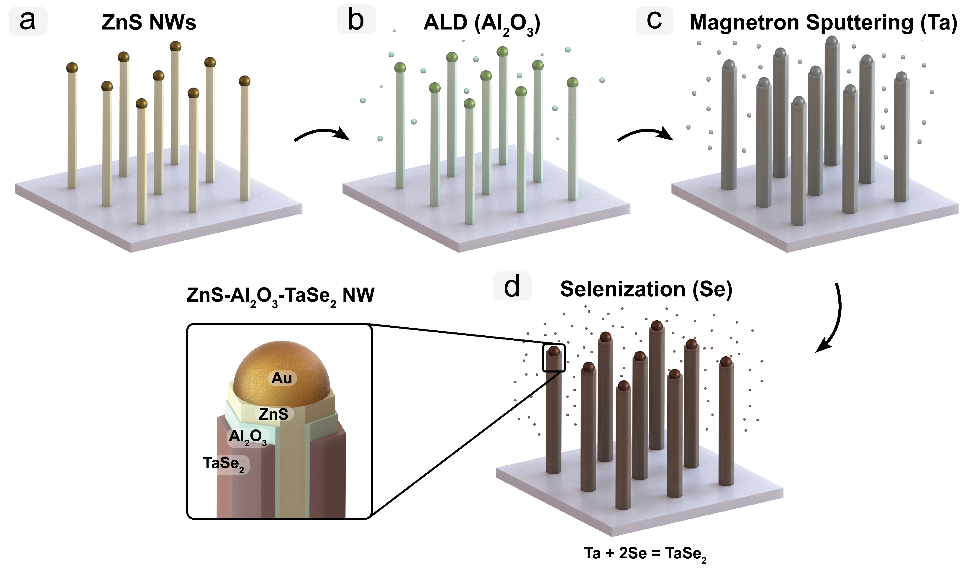
Abstract
:1. Introduction
2. Experimental Details
2.1. Materials and Methods
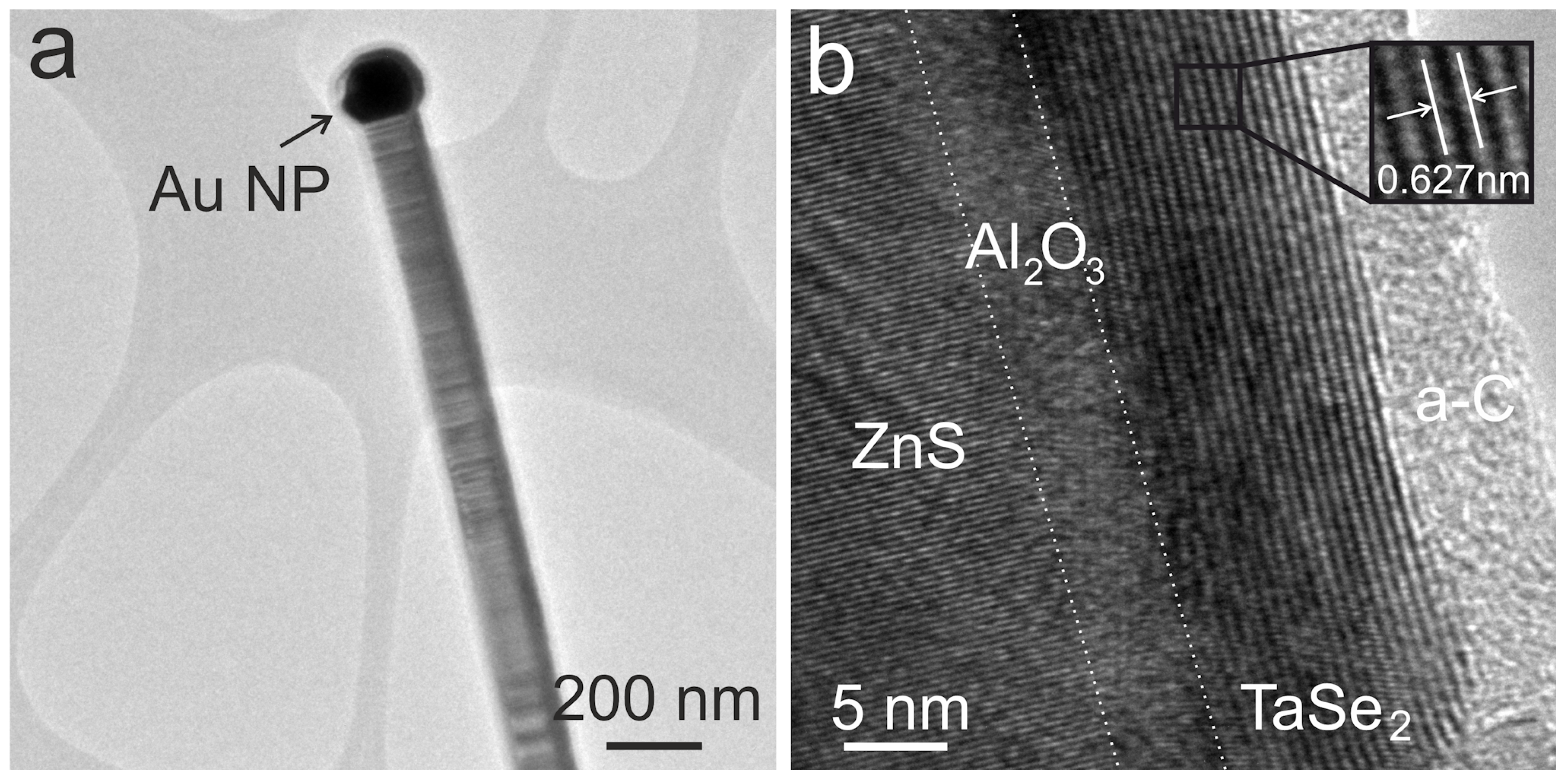
- In the initial step, ZnS NWs were synthesized on top of the oxidized silicon wafers Si/SiO2 (Si(100) wafer, 50 nm of thermal oxide, Semiconductor Wafer, Inc., Hsinchu, Taiwan) using the Au nanoparticles (50 nm in diameter, water suspension, BBI International, Grand Forks, ND, USA) as a catalyst for vapor–liquid–solid (VLS) growth. ZnS powder 0.4 g (>97%, Sigma Aldrich, St. Louis, MO, USA) was thermally sublimated in a quartz tube reactor at a temperature of 950 °C for 30 min, followed by natural cooling. The ZnS vapor was carried downstream by a Ar/H2 35% gas mixture to the substrate to grow ZnS NWs.
- Subsequently, a thin Al2O3 layer was deposited on the NWs using the ALD technique in a Savannah S100 reactor. The deposition process, carried out at 150 °C, involved 66 cycles (Al2O3 thickness ∼6 nm) of alternating Trimethylaluminum (TMA) and H2O as precursors, with N2 serving as the inert carrier gas.
- A Ta metallic layer, approximately 15 nm thick on flat substrates, was deposited over the ZnS/Al2O3 NWs using direct current (DC) magnetron sputtering from a Ta target in an Ar atmosphere ( torr, 30 sccm Ar gas flow at 100 W DC power). It is noteworthy that, due to geometrical factors, the actual thickness of the Ta film on the vertical NWs might be less than 15 nm.
- The final step was the annealing of the coated NWs in a selenium environment. The samples underwent a 50-min anneal at 650 °C within a vacuum-sealed quartz ampoule to transform the metallic Ta layer into TaSe2. The procedure involved placing the Si/SiO2 wafer with ZnS/Al2O3/Ta NWs or a Ta thin film on Si/SiO2 inside the ampoule, which was then evacuated using a turbo pump (vacuum better than torr) and hermetically sealed. Selenium pellets (50 mg, Sigma Aldrich) and Ta foil (100 mg, GoodFellow, Huntingdon, UK) were also introduced into the ampoule to maintain a stable vapor pressure of TaSe2 and to minimize the vapor’s transport to cooler areas of the ampoule. The length of ampoule was tailored to align with the hot zone of the oven, ensuring that its ends remained cooler, which, in turn, allowed for the condensation of any unreacted selenium (Figure S2, Supplementary data).
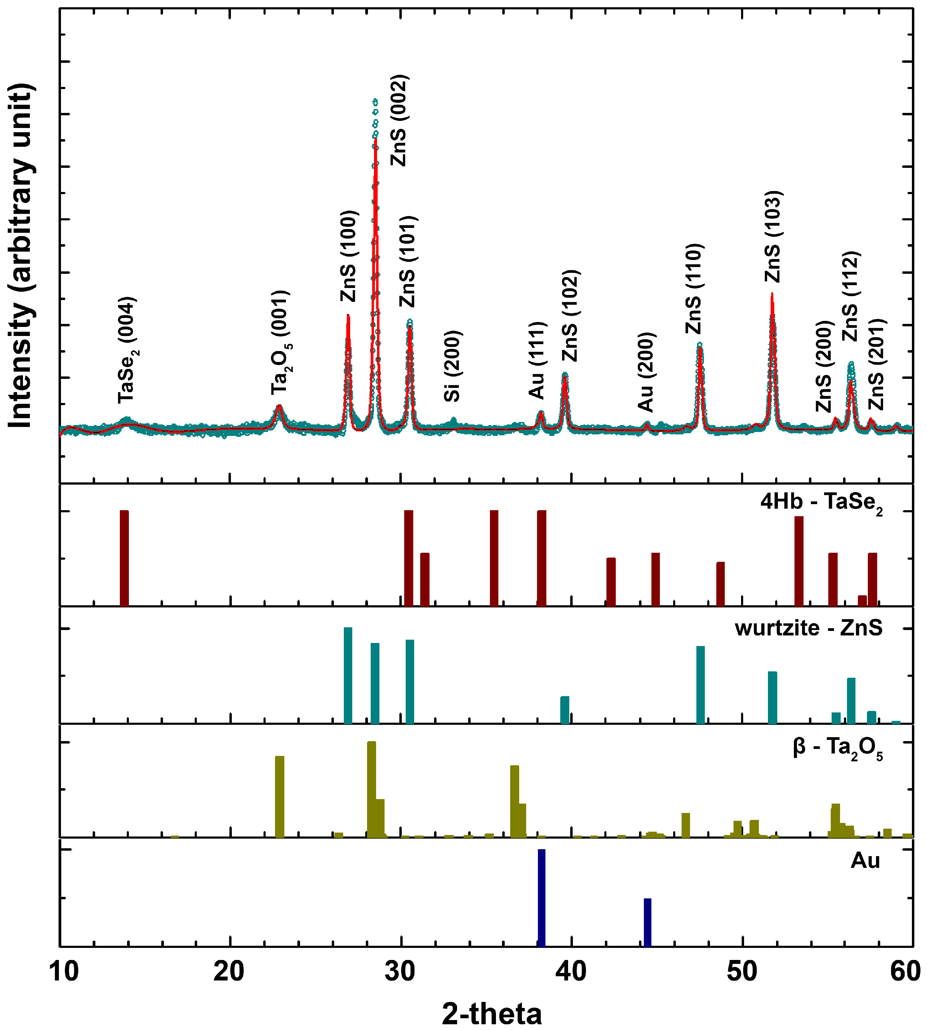
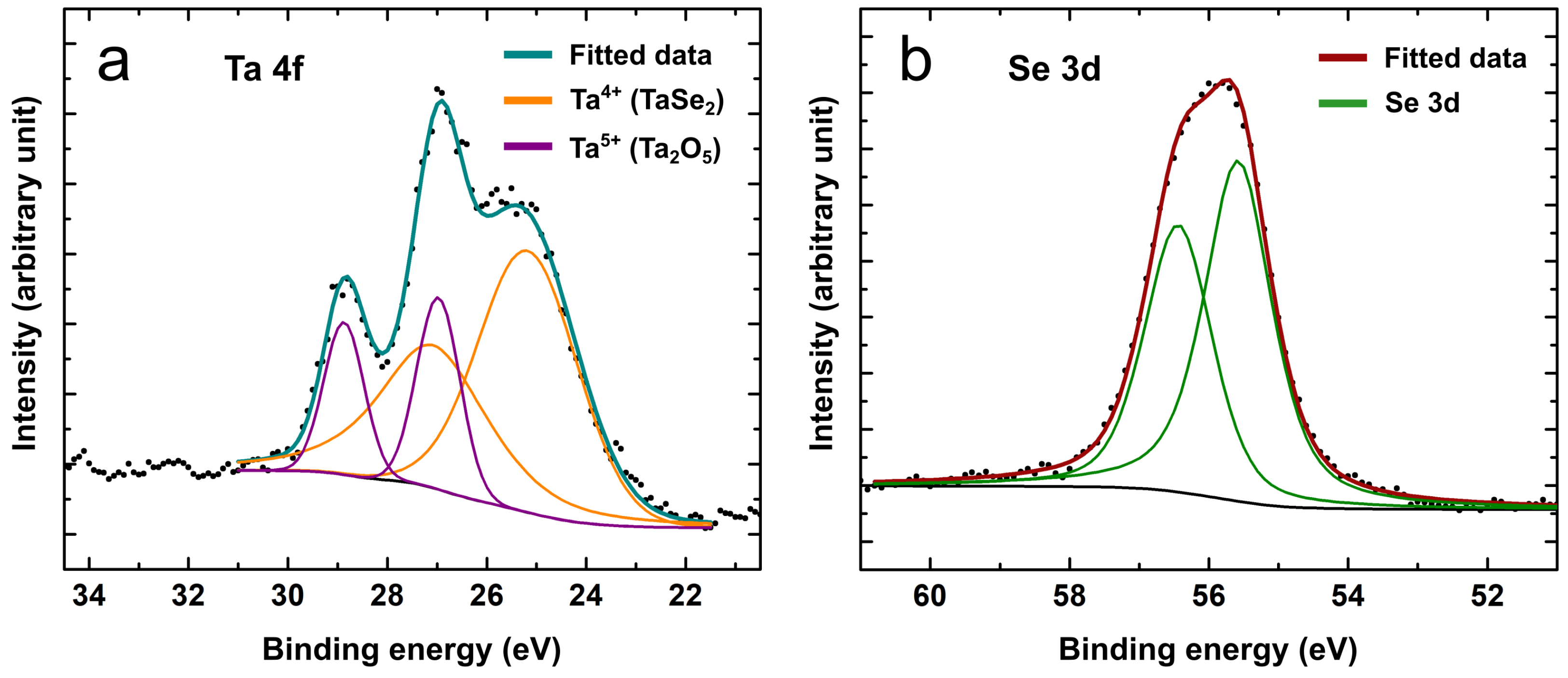
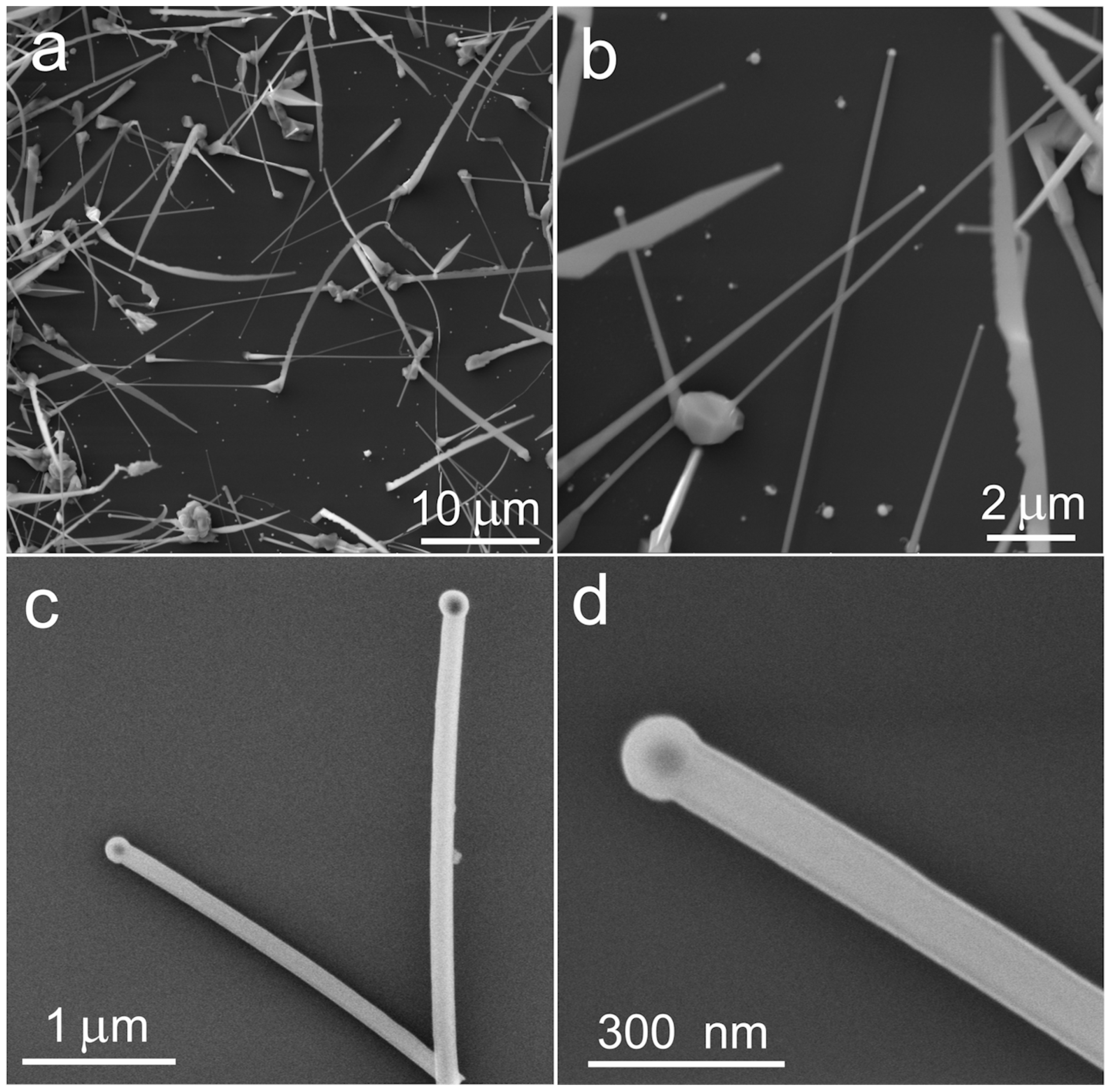
2.2. Characterisation
3. Results and Discussion
4. Conclusions
Supplementary Materials
Author Contributions
Funding
Data Availability Statement
Acknowledgments
Conflicts of Interest
References
- Yin, X.; Tang, S.; Zheng, Y.; Gao, J.; Wu, J.; Zhang, H.; Chhowalla, M.; Chen, W.; Wee, A. Recent developments in 2D transition metal dichalcogenides: Phase transition and applications of the (quasi-)metallic phases. Chem. Soc. Rev. 2021, 50, 10087–10115. [Google Scholar] [CrossRef] [PubMed]
- Ali, H.G.; Khan, K.; Hanif, M.; Khan, M.Z.; Hussain, I.; Javed, M.S.; AL-bonsrulah, H.A.; Mosiałek, M.; Fichtner, M.; Motola, M. Advancements in two-dimensional materials as anodes for lithium-ion batteries: Exploring composition-structure-property relationships, emerging trends, and future perspective. J. Energy Storage 2023, 73, 108980. [Google Scholar] [CrossRef]
- Wang, Q.H.; Kalantar-Zadeh, K.; Kis, A.; Coleman, J.N.; Strano, M.S. Electronics and optoelectronics of two-dimensional transition metal dichalcogenides. Nat. Nanotechnol. 2012, 7, 699–712. [Google Scholar] [CrossRef] [PubMed]
- Jariwala, D.; Sangwan, V.K.; Lauhon, L.J.; Marks, T.J.; Hersam, M.C. Emerging Device Applications for Semiconducting Two-Dimensional Transition Metal Dichalcogenides. ACS Nano 2014, 8, 1102–1120. [Google Scholar] [CrossRef] [PubMed]
- Manzeli, S.; Ovchinnikov, D.; Pasquier, D.; Yazyev, O.; Kis, A. 2D transition metal dichalcogenides. Nat. Rev. Mater. 2017, 2, 17033. [Google Scholar] [CrossRef]
- Lasek, K.; Li, J.; Kolekar, S.; Coelho, P.M.; Guo, L.; Zhang, M.; Wang, Z.; Batzill, M. Synthesis and characterization of 2D transition metal dichalcogenides: Recent progress from a vacuum surface science perspective. Surf. Sci. Rep. 2021, 76, 100523. [Google Scholar] [CrossRef]
- Ali, S.; Ahmad Shah, S.S.; Sufyan Javed, M.; Najam, T.; Parkash, A.; Khan, S.; Bajaber, M.A.; Eldin, S.M.M.; Tayeb, R.A.; Rahman, M.M.; et al. Recent Advances of Transition Metal Dichalcogenides-Based Materials for Energy Storage Devices, in View of Monovalent to Divalent Ions. Chem. Rec. 2023, 24, e202300145. [Google Scholar] [CrossRef]
- Choi, W.; Choudhary, N.; Han, G.; Park, J.; Akinwande, D.; Lee, Y. Recent development of two-dimensional transition metal dichalcogenides and their applications. Mater. Today 2017, 20, 116–130. [Google Scholar] [CrossRef]
- Hossain, M.; Zhao, Z.; Wen, W.; Wang, X.; Wu, J.; Xie, L. Recent Advances in Two-Dimensional Materials with Charge Density Waves: Synthesis, Characterization and Applications. Crystals 2017, 7, 298. [Google Scholar] [CrossRef]
- Wang, H.; Chen, Y.; Zhu, C.; Wang, X.; Zhang, H.; Tsang, S.; Li, H.; Lin, J.; Yu, T.; Liu, Z.; et al. Synthesis of Atomically Thin 1T-TaSe2 with a Strongly Enhanced Charge-Density-Wave Order. Adv. Funct. Mater. 2020, 30, 2001903. [Google Scholar] [CrossRef]
- Lüdecke, J.; van Smaalen, S.; Spijkerman, A.; de Boer, J.L.; Wiegers, G.A. Commensurately modulated structure of 4Hb—TaSe2 determined by X-ray crystal-structure refinement. Phys. Rev. B 1999, 59, 6063–6071. [Google Scholar] [CrossRef]
- Samnakay, R.; Wickramaratne, D.; Pope, T.; Lake, R.; Salguero, T.; Balandin, A. Zone-Folded Phonons and the Commensurate–Incommensurate Charge-Density-Wave Transition in 1T-TaSe2 Thin Films. Nano Lett. 2015, 15, 2965–2973. [Google Scholar] [CrossRef] [PubMed]
- Bjerkelund, E.; Kjekshus, A. On the structural properties of the Ta1+xSe2. Acta Chem. Scand. 1967, 21, 513–526. [Google Scholar] [CrossRef]
- Liu, S.; Tang, Z.R.; Sun, Y.; Colmenares, J.; Xu, Y.J. One-dimension-based spatially ordered architectures for solar energy conversion. Chem. Soc. Rev. 2015, 44, 5053–5075. [Google Scholar] [CrossRef]
- Lin, Y.P.; Polyakov, B.; Butanovs, E.; Popov, A.; Sokolov, M.; Bocharov, D.; Piskunov, S. Excited states calculations of MoS2@ZnO and WS2@ZnO two-dimensional nanocomposites for water-splitting applications. Energies 2022, 15, 150. [Google Scholar] [CrossRef]
- Liu, Y.; Xie, S.; Li, H.; Wang, X. A highly efficient sunlight driven ZnO nanosheet photocatalyst: Synergetic effect of P-doping and MoS2 atomic layer loading. ChemCatChem 2014, 6, 2522–2526. [Google Scholar] [CrossRef]
- Aldalbahi, A.; Wang, Z.B.; Ahamad, T.; Alshehri, S.; Feng, P. Two-step facile preparation of 2D MoS2/ZnO nanocomposite p-n junctions with enhanced photoelectric performance. Int. J. Photoenergy 2021, 2021, e1884293. [Google Scholar] [CrossRef]
- Butanovs, E.; Vlassov, S.; Kuzmin, A.; Piskunov, S.; Butikova, J.; Polyakov, B. Fast-response single-nanowire photodetector based on ZnO/WS2 core/shell heterostructures. ACS Appl. Mater. Interfaces 2018, 10, 13869–13876. [Google Scholar] [CrossRef]
- Han, S.; Meng, Y.; Xu, Z.; Kim, J.S.; Li, Y.; Roh, I.; Ahn, H.; Kim, D.; Bae, S. Freestanding Membranes for Unique Functionality in Electronics. ACS Appl. Electron. Mater. 2023, 5, 690–704. [Google Scholar] [CrossRef]
- Ong, H.; Chang, R. Optical constants of wurtzite ZnS thin films determined by spectroscopic ellipsometry. Appl. Phys. Lett. 2001, 79, 3612–3614. [Google Scholar] [CrossRef]
- Dimitrova, V.; Tate, J. Synthesis and characterization of some ZnS-based thin film phosphors for electroluminescent device applications. Thin Solid Films 2000, 365, 134–138. [Google Scholar] [CrossRef]
- Fang, X.; Zhai, T.; Gautam, U.; Li, L.; Wu, L.; Bando, Y.; Golberg, D. ZnS nanostructures: From synthesis to applications. Prog. Mater. Sci. 2011, 56, 175–287. [Google Scholar] [CrossRef]
- Sperling, B.; Kalanyan, B.; Maslar, J. Atomic Layer Deposition of Al2O3 Using Trimethylaluminum and H2O: The Kinetics of the H2O Half-Cycle. J. Phys. Chem. C 2020, 124, 3410–3420. [Google Scholar] [CrossRef]
- Prokes, S.; Katz, M.; Twigg, M. Growth of crystalline Al2O3 via thermal atomic layer deposition: Nanomaterial phase stabilization. APL Mater. 2014, 2, 032105. [Google Scholar] [CrossRef]
- Vlassov, S.; Polyakov, B.; Vahtrus, M.; Mets, M.; Antsov, M.; Oras, S.; Tarre, A.; Arroval, T.; Lohmus, R.; Aarik, J. Enhanced flexibility and electron-beam-controlled shape recovery in alumina-coated Au and Ag core-shell nanowires. Nanotechnology 2017, 28, 505707. [Google Scholar] [CrossRef] [PubMed]
- Butanovs, E.; Kuzmin, A.; Zolotarjovs, A.; Vlassov, S.; Polyakov, B. The role of Al2O3 interlayer in the synthesis of ZnS/Al2O3/MoS2 core-shell nanowires. J. Alloys Compd. 2022, 165648. [Google Scholar] [CrossRef]
- Shi, J.; Chen, X.; Zhao, L.; Gong, Y.; Hong, M.; Huan, Y.; Zhang, Z.; Yang, P.; Li, Y.; Zhang, Q.; et al. Chemical Vapor Deposition Grown Wafer-Scale 2D Tantalum Diselenide with Robust Charge-Density-Wave Order. Adv. Mater. 2018, 30, 1804616. [Google Scholar] [CrossRef]
- Pligovka, A.; Lazavenka, A.; Turavets, U.; Hoha, A.; Salerno, M. Two-Level 3D Column-like Nanofilms with Hexagonally–Packed Tantalum Fabricated via Anodizing of Al/Nb and Al/Ta Layers—A Potential Nano-Optical Biosensor. Materials 2023, 16, 993. [Google Scholar] [CrossRef]
- Butanovs, E.; Kuzmin, A.; Piskunov, S.; Smits, K.; Kalinko, A.; Polyakov, B. Synthesis and characterization of GaN/ReS2, ZnS/ReS2 and ZnO/ReS2 core/shell nanowire heterostructures. Appl. Surf. Sci. 2021, 536, 147841. [Google Scholar] [CrossRef]
- Rao, C.; Rao, G. Transition Metal Oxides; Department of Chemistry, Indian Institute of Technology: Kanpur, India, 1974. [Google Scholar]
- Patnaik, P. Handbook of Inorganic Chemicals; McGraw-Hill: New York, NY, USA, 2003. [Google Scholar]
- Li, P.; Stender, C.; Ringe, E.; Marks, L.D.; Odom, T.W. Synthesis of TaS2 Nanotubes From Ta2O5 Nanotube Templates. Small 2010, 6, 1096–1099. [Google Scholar] [CrossRef]
- Najafi, L.; Bellani, S.; Oropesa-Nuñez, R.; Martín-García, B.; Prato, M.; Pasquale, L.; Panda, J.K.; Marvan, P.; Sofer, Z.; Bonaccorso, F. TaS2, TaSe2, and Their Heterogeneous Films as Catalysts for the Hydrogen Evolution Reaction. ACS Catal. 2020, 10, 3313–3325. [Google Scholar] [CrossRef]
- Sim, Y.; Chae, Y.; Kwon, S.Y. Recent advances in metallic transition metal dichalcogenides as electrocatalysts for hydrogen evolution reaction. iScience 2022, 25, 105098. [Google Scholar] [CrossRef]
- Wang, M.; Zhang, L.; Huang, M.; Liu, Y.; Zhong, Y.; Pan, J.; Wang, Y.; Zhu, H. Morphology-controlled Tantalum Diselenide Structures as Self-optimizing Hydrogen Evolution Catalysts. Energy Environ. Mater. 2020, 3, 12–18. [Google Scholar] [CrossRef]
- Doebelin, N.; Kleeberg, R. Profex: A graphical user interface for the Rietveld refinement program BGMN. J. Appl. Crystallogr. 2015, 48, 1573–1580. [Google Scholar] [CrossRef]
- Ulrich, F.; Zachariasen, W.H. Ueber die kristallstruktur des alpha- und beta-CdS, sowie des wurtzits. Z. Fur Krist. 1925, 62, 260–273. [Google Scholar]
- McMurdie, H.F.; Morris, M.C.; Evans, E.H.; Paretzkin, B.; Wong-Ng, W.; Ettlinger, L.; Hubbard, C.R. Standard X-Ray Diffraction Powder Patterns from the JCPDS Research Associateship. Powder Diffr. 1986, 1, 64–77. [Google Scholar] [CrossRef]
- Moon, H.; Nam, C.; Kim, C.; Kim, B. Synthesis and photoluminescence of zinc sulfide nanowires by simple thermal chemical vapor deposition. Mater. Res. Bull. 2006, 41, 2013–2017. [Google Scholar] [CrossRef]
- Aleshina, L.A.; Loginova, S.V. Rietveld analysis of X-ray diffraction pattern from β-Ta2O5 oxide. Crystallogr. Rep. 2002, 47, 415–419. [Google Scholar] [CrossRef]
- Yang, Y.; Kawazoe, Y. Prediction of new ground-state crystal structure of Ta2O5. Phys. Rev. Mater. 2018, 2, 034602. [Google Scholar] [CrossRef]
- Lawan Adam, M.; Buba Garba, I.; Alhaji Bala, A.; Aji Suleiman, A.; Muhammad Gana, S.; Lawan Adam, F. Tuning superconductivity and charge density wave order in TaSe2 through Pt intercalation. Phys. Rev. B 2023, 107, 104510. [Google Scholar] [CrossRef]
- Swanson, H.E.; Tatge, E. Standard X-ray Diffraction Powder Patterns; National Bureau of Standards (U.S.) Circular Nr. 539; National Bureau of Standards: Gaithersburg, MD, USA, 1953; Section I, 33.
- Wyckoff, R.W.G. Crystal Structures, 2nd ed.; Interscience Publishers: New York, NY, USA, 1963; Volume 1. [Google Scholar]
- Luo, H.; Xie, W.; Tao, J.; Pletikosic, I.; Valla, T.; Sahasrabudhe, G.S.; Osterhoudt, G.; Sutton, E.; Burch, K.S.; Seibel, E.M.; et al. Differences in Chemical Doping Matter: Superconductivity in Ti1−xTaxSe2 but Not in Ti1−xNbxSe2. Chem. Mater. 2016, 28, 1927–1931. [Google Scholar] [CrossRef]


Disclaimer/Publisher’s Note: The statements, opinions and data contained in all publications are solely those of the individual author(s) and contributor(s) and not of MDPI and/or the editor(s). MDPI and/or the editor(s) disclaim responsibility for any injury to people or property resulting from any ideas, methods, instructions or products referred to in the content. |
© 2024 by the authors. Licensee MDPI, Basel, Switzerland. This article is an open access article distributed under the terms and conditions of the Creative Commons Attribution (CC BY) license (https://creativecommons.org/licenses/by/4.0/).
Share and Cite
Polyakov, B.; Kadiwala, K.; Butanovs, E.; Dipane, L.; Trausa, A.; Bocharov, D.; Vlassov, S. Synthesis of ZnS/Al2O3/TaSe2 Core/Shell Nanowires Using Thin Ta Metal Film Precursor. ChemEngineering 2024, 8, 25. https://doi.org/10.3390/chemengineering8010025
Polyakov B, Kadiwala K, Butanovs E, Dipane L, Trausa A, Bocharov D, Vlassov S. Synthesis of ZnS/Al2O3/TaSe2 Core/Shell Nanowires Using Thin Ta Metal Film Precursor. ChemEngineering. 2024; 8(1):25. https://doi.org/10.3390/chemengineering8010025
Chicago/Turabian StylePolyakov, Boris, Kevon Kadiwala, Edgars Butanovs, Luize Dipane, Annamarija Trausa, Dmitry Bocharov, and Sergei Vlassov. 2024. "Synthesis of ZnS/Al2O3/TaSe2 Core/Shell Nanowires Using Thin Ta Metal Film Precursor" ChemEngineering 8, no. 1: 25. https://doi.org/10.3390/chemengineering8010025