Article

Phases and Interfaces in the Cr–Fe–Si Ternary System: X-ray Diffraction and Electron Microscopy Study

by
Elena I. Suvorova
1,*,
Natalya A. Arkharova
1,
Anna G. Ivanova
1,
Fedor Yu. Solomkin
2 and
Philippe A. Buffat
3
1
A.V. Shubnikov Institute of Crystallography, Federal Scientific Research Centre “Crystallography and Photonics” of the Russian Academy of Sciences, Leninsky pr. 59, Moscow 119333, Russia
2
Ioffe Physical Technical Institute of Russian Academy of Sciences, Polytechnic Street, 26, St. Petersburg 194021, Russia
3
Ecole Polytechnique Fédérale de Lausanne, Centre Interdisciplinaire de Microscopie Electronique, CH-1015 Lausanne, Switzerland
*
Author to whom correspondence should be addressed.
Inorganics 2023, 11(2), 73; https://doi.org/10.3390/inorganics11020073
Submission received: 31 December 2022 / Revised: 23 January 2023 / Accepted: 29 January 2023 / Published: 3 February 2023
(This article belongs to the Special Issue Inorganics: 10th Anniversary)

Abstract

:
The ternary Cr-Fe-Si system was investigated with X-ray diffraction, energy dispersive X-ray spectrometry, scanning and transmission electron microscopy, and electron diffraction. Samples melted at 1723 K were examined right after cooling or after annealing at 1073 K for 3 days to determine phases, grain sizes, and interphase interfaces. During annealing, a polymorphic transformation of the tetragonal α-FeSi2 to the orthorhombic β-FeSi2 phase occurs, while CrSi2 retains its hexagonal structure at high-temperature treatment. Thin layers of ε-FeSi with a cubic structure were observed and identified within the CrSi2 grains. Crystallographic orientation relationships are determined at the interphase interfaces. The contributions of lattice mismatch and thermal expansion coefficient misfit to deformation are discussed.

1. Introduction

Binary iron and chromium silicides attracted much interest due to their intrinsic qualities (crystal chemistry, phase diagram, phase transitions, dependance of physical properties on stoichiometry) and their technological importance for the production of thermoelectric and microelectronic materials. The Cr-Fe-Si ternary system has been much less studied, although it is of definite industrial and technological importance. Examples include applications in commercial alloy steels, anode materials for rechargeable Li-ion batteries, electromagnetic wave absorbers for mobile phones, and soft magnetic materials and some special applications in high temperature thermoelectric materials [1,2,3,4]. For thermoelectric applications, the two semiconducting silicides CrSi2 and β-FeSi2 are known as environmentally friendly and low-cost materials [5,6,7,8]. However, their efficiency expressed by the dimensionless figure of merit ZT, is less than 1. Therefore, several concepts have been developed to achieve ZT > 1, including a concept based on enhanced phonon scattering through interfaces, the grain boundaries, and nano-inclusions in nanocomposites to reduce thermal conductivity [9,10].
It is known that synthesis of a ternary Fe–Si–Cr alloys (arc melting, high temperature pressing, mechanical allowing, sintering) is usually carried out at high temperature and leads to formation of different Cr and Fe silicides [11,12,13,14]. Much attention has been paid to the study of the properties (structural, mechanical, thermodynamic, electrical, magnetic, etc.) of different phases of iron and chromium silicides. See, for instance, the studies and syntheses [15,16,17,18,19,20,21,22,23]. It should be noted that the structure of binary iron or chromium silicides has been studied separately either at the micro- or nano-metric scale in the case of thin films or nanocrystals [24,25,26,27,28,29].
The goal of the present work was the investigation at the micro- and nanoscale of the composition and distribution of phases in Fe-Si-Cr ternary systems, both bulk and annealed, as well as their morphology and distribution, to help to establish a solid basis for the design of new thermoelectric devices oriented towards specific properties. Particular attention has been paid to the study of mutual spatial distribution, grain shape and size, determination of crystallographic orientation relationships at the interfaces between adjacent grains, presence of impurities in the grains. Quantitative analysis of the elemental phases was carried out on large areas or at the nanoscale by analytical scanning and transmission electron microscopy, respectively.

2. Results

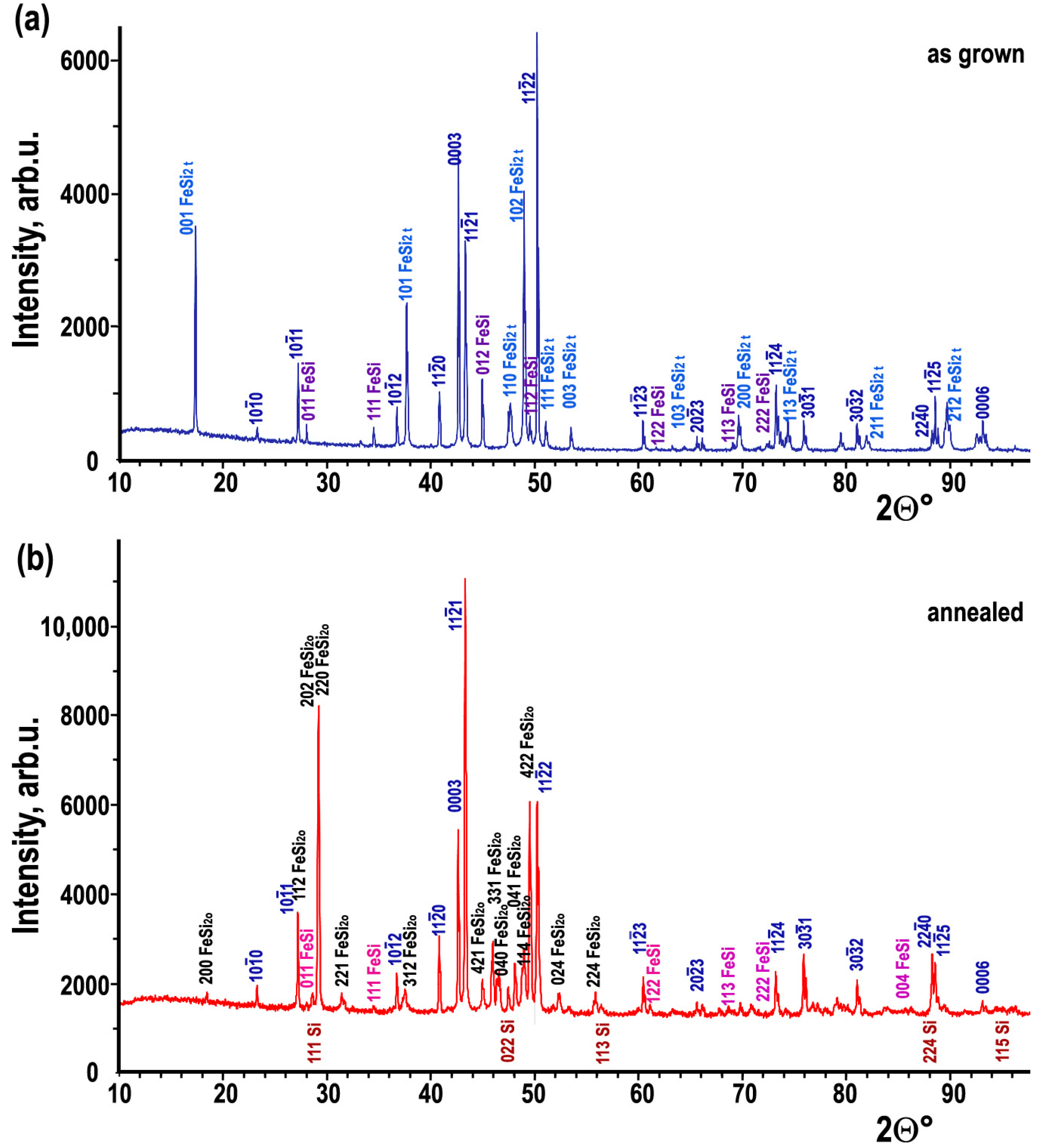
2.1. Powder X-ray Diffraction Study

In accordance with Cr-Fe-Si ternary phase diagrams [13,14], the position of the sample composition of FeCrSi4 is at the point 17 at% Cr: 17 at % Fe: 66 Si at.%. Thus, we expected the following phases to be formed: FeSi2, CrSi2, and (Cr, Fe)Si for the temperature interval and starting stoichiometric composition used in the work. Close to this point, pure Si can also be formed.
The possible phases, their lattice parameters and space groups of the Cr and Fe silicides and Si used in this work for identification are listed in Table 1 according to corresponding ICSD database (FIZ Karlsruhe, Germany) and references. We will use general notations for phases of iron silicides: α-FeSi2 (tetragonal structure), β-FeSi2 (orthorhombic structure) and ε-FeSi (cubic structure).
The Rietveld refined powder XRD patterns obtained from the samples are shown in Figure 1. The reflections on the XRD patterns from the sample before annealing can be indexed with three phases tetragonal α-FeSi2, hexagonal CrSi2, and cubic FeSi (Figure 1a). While the XRD pattern obtained from the annealed material shows the presence of four phases orthorhombic β-FeSi2, hexagonal CrSi2, cubic ε-FeSi, and cubic Si (Figure 1b). No cubic CrSi was revealed in any of the samples, nor was any traces of α-FeSi2 found in the annealed sample. Thus, α-FeSi2 phase with space group P4/mmm completely transforms into orthorhombic Cmca β-FeSi2 phase and silicon appears in the composition of the sample after 3 days of annealing at 1073 K.
The quantitative composition of phases in the samples together with the Rwp (weighted least-squares error) and GOF (goodness of fit) in accordance with Rietveld refinement are reported in Table 2. It shows that CrSi2 hex has retained its space group and quantity, while iron disilicide has undergone a tetragonal to orthorhombic phase transition due to the tetragonal FeSi2 phase and partly of cubic ε−FeSi phase.
The presence of minor other phases found by TEM will be described later in the article. (See for instance Section 2.3 and the corresponding figures).

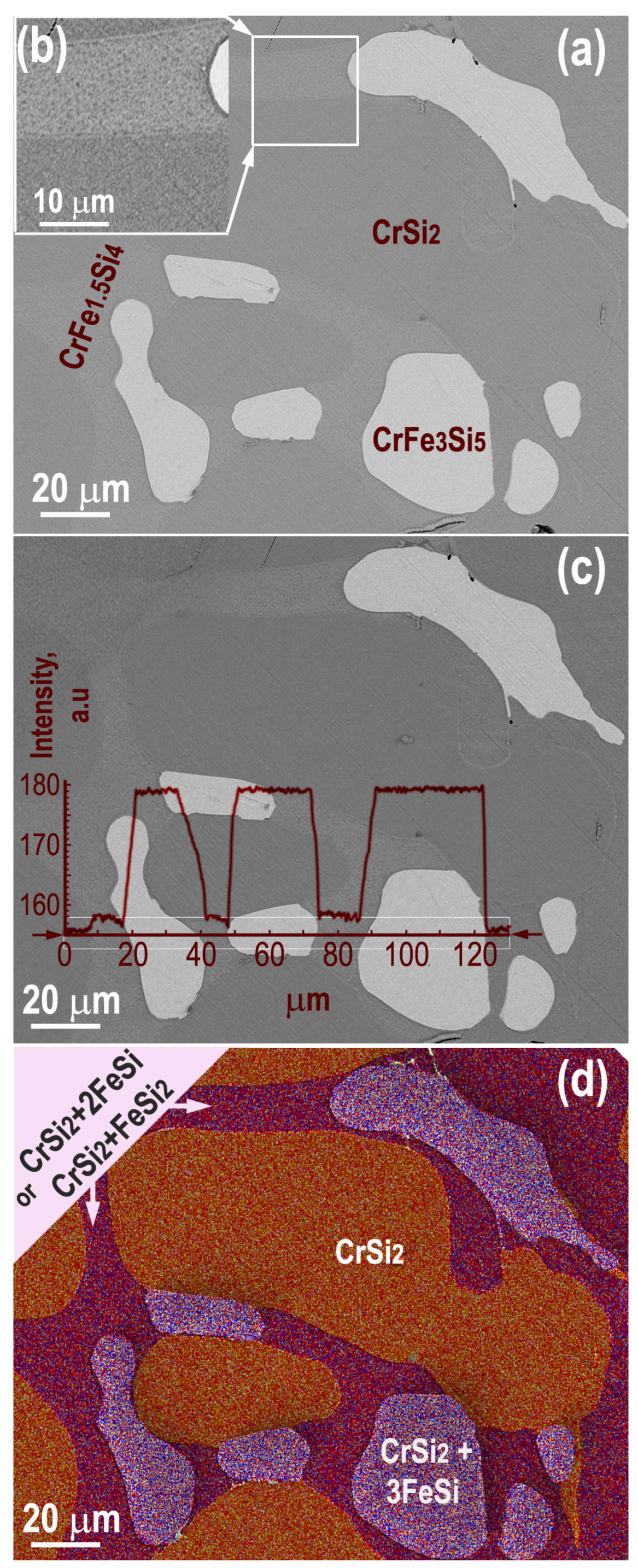
2.2. SEM and EDXS Analysis

Information on grain morphology, size, shape, and distribution over large areas was collected by scanning electron microscopy (SEM) using secondary electron (SE) and backscatter electron (BSE) imaging. In parallel, contrast analysis of the BSE images and elemental analysis by energy dispersive X-ray spectrometry (EDXS) provided chemical contrast and at least semi-quantitative elemental analysis to distinguish grains by their nature.
Figure 2a shows a view of a polished section in an as-grown sample in backscattered electron mode (BSE). The brightness of the image essentially reflects the atomic number of the object (“Z-contrast”), and the contrasts differentiate the regions according to their effective atomic numbers; thus, their different chemical compositions [51,52]. As the number of BSE electrons increases monotonically with the atomic number, the higher the effective atomic number, the brighter the area. This rapid access to chemical contrast is particularly effective for tracking the distribution of different phases, but insufficient for distinguishing phases or phase mixtures of similar effective atomic numbers. Therefore, an initial estimate of the composition by BSE must be refined by EDXS chemical analysis. In addition, the acceleration voltage should be as low as possible to reduce the penetration depth of the electrons, thus the risk of superposition of different phases, but still high enough to detect all elements present. In this case, 12 kV was chosen as a fair compromise that covers all lines up to Fe-K.
The general chemical formulas obtained from microanalysis data on each of the three different grey areas: the darkest, intermediate, and brightest, which corresponds to CrSi2, CrFe1.5Si4, and CrFe3Si5, respectively (Figure 2a). Taking in account the XRD observation that led to a material made of the three phases CrSi2, α-FeSi2 and FeSi, the darkest area can be understood as to the single phase CrSi2, the brightest as a mixture of the CrSi2 + 3FeSi phased and the intermediate as CrSi2 + FeSi2 or CrSi2 + 2FeSi (within the uncertainty of the EDXS data). The inset (Figure 2b) shows clearly that the intermediate gray area contains a mixture of fine-grained phases. In addition, the brighter lines at interfaces suggest the presence of a higher Z interfacial phase.
To compare the BSE contrast to the assumed phases we used the Reuter method recommended by Goldstein [53]. We estimated and compared the relative ratio <ZAB>2 between several possible Fe and Cr silicides and their combinations with the relative ratio of experimental intensity. BSE line scan intensity profiles like on Figure 2c were used to find the relative intensities from different grains. For the darkest gray area, the intensity was 155 a. u., for the intermediate gray area the intensity was about 157 a.u., and for the brightest area the intensity value reached 179 a.u.
It was found a very good agreement between the calculated (for average atomic numbers) and the experimental ratios (for intensity on the SEM BSE image). Such agreement together with the EDXS microanalysis data allowed to conclude that that the brightest regions in the SEM image (Figure 2) belong to a mixture of CrSi2 and FeSi phases with the ratio CrSi2–3FeSi. While light grey areas seen with the SEM are interconnected and constitute a net that may be a matrix enclosing the dark grey and bright areas consisting of CrSi2 and FeSi2, a combination CrSi2–2FeSi cannot be excluded.
The different phases are indicated by specific colors on the EDXS concentration map (Figure 2d). Isolated pure CrSi2 grains have the largest size, from several tens of µm to more than one hundred µm. They are surrounded by a continuous network of a mixture of either FeSi2 + CrSi2 or 2FeSi + CrSi2 phases that appear homogeneous at the resolution of this SEM analysis. Within this network, finer grains have formed that contain a mixture of 3FeSi + CrSi2 phases that is also homogeneous at this scale. The fine granularity of this EDXS concentration map is due to the statistical noise of the quantification procedure.
The results show that large grains of CrSi2 of several tens (even more than 100 μm) in size are quite homogeneous, while the FeSi2 or FeSi phase always exists in combination with CrSi2. The true phase composition was investigated with TEM, EDXS, and transmission electron diffraction.

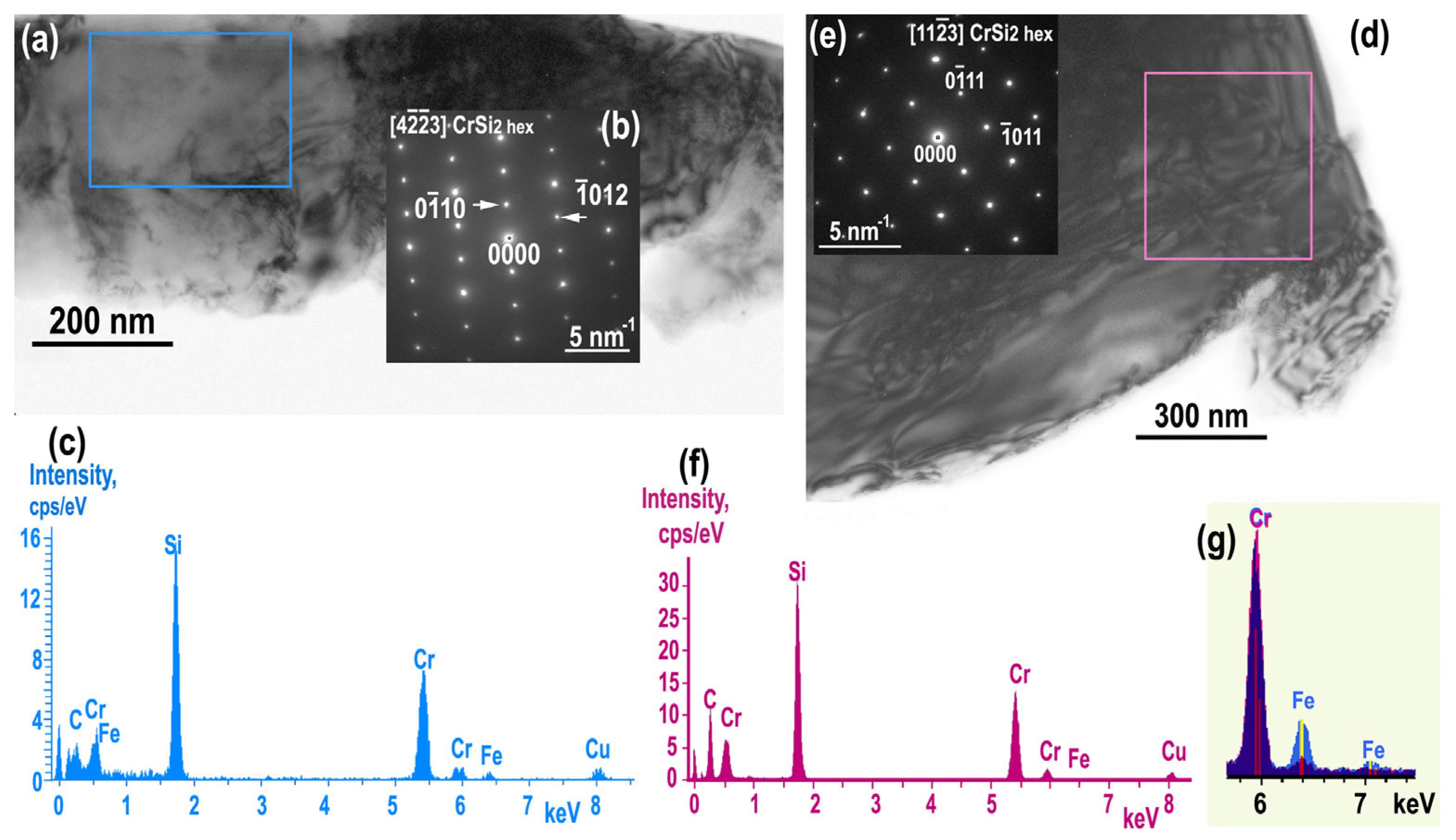
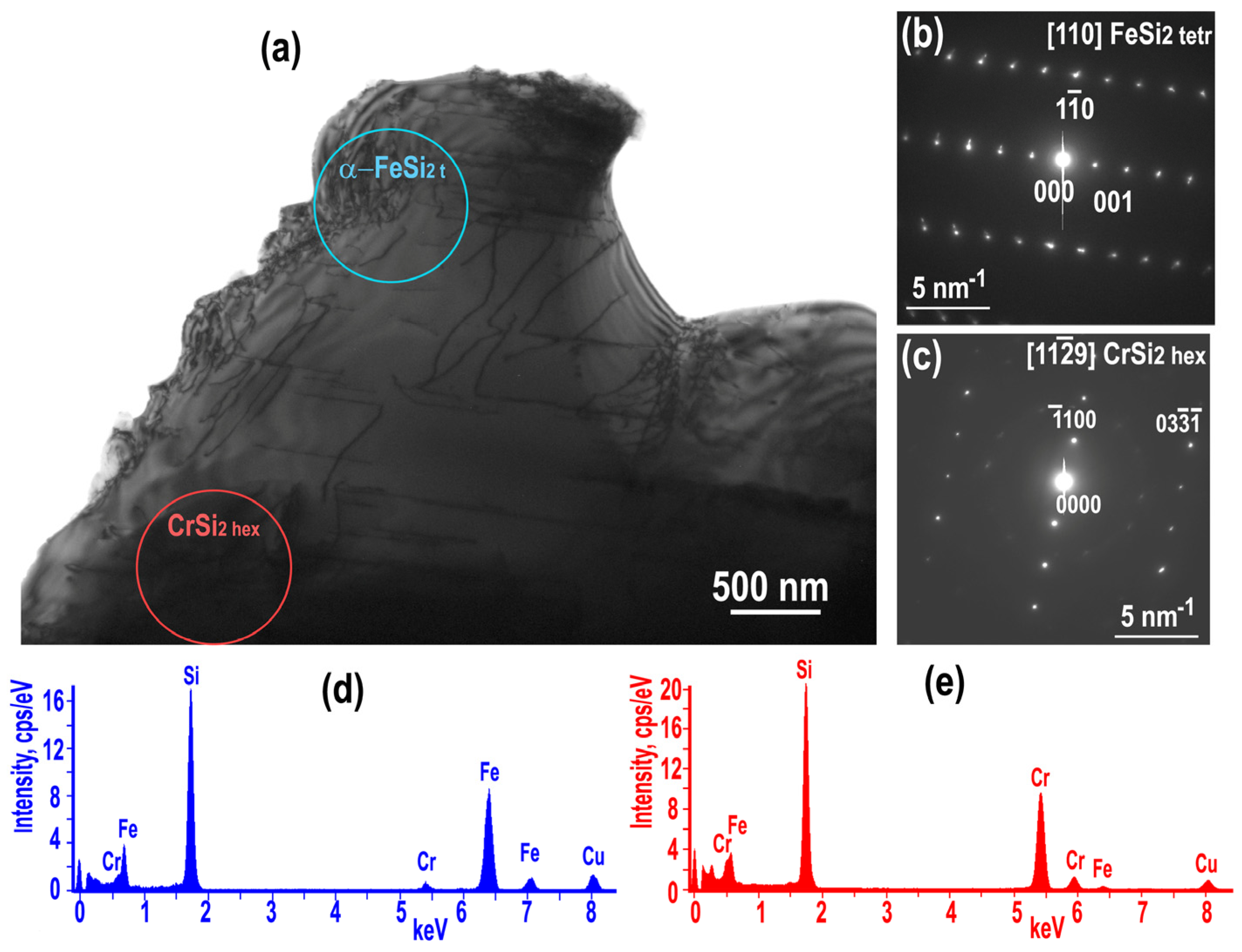
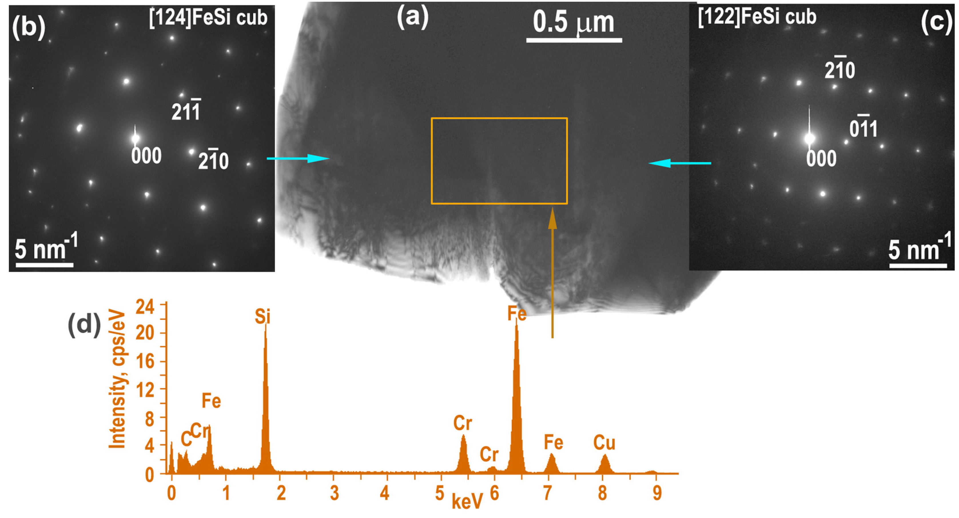
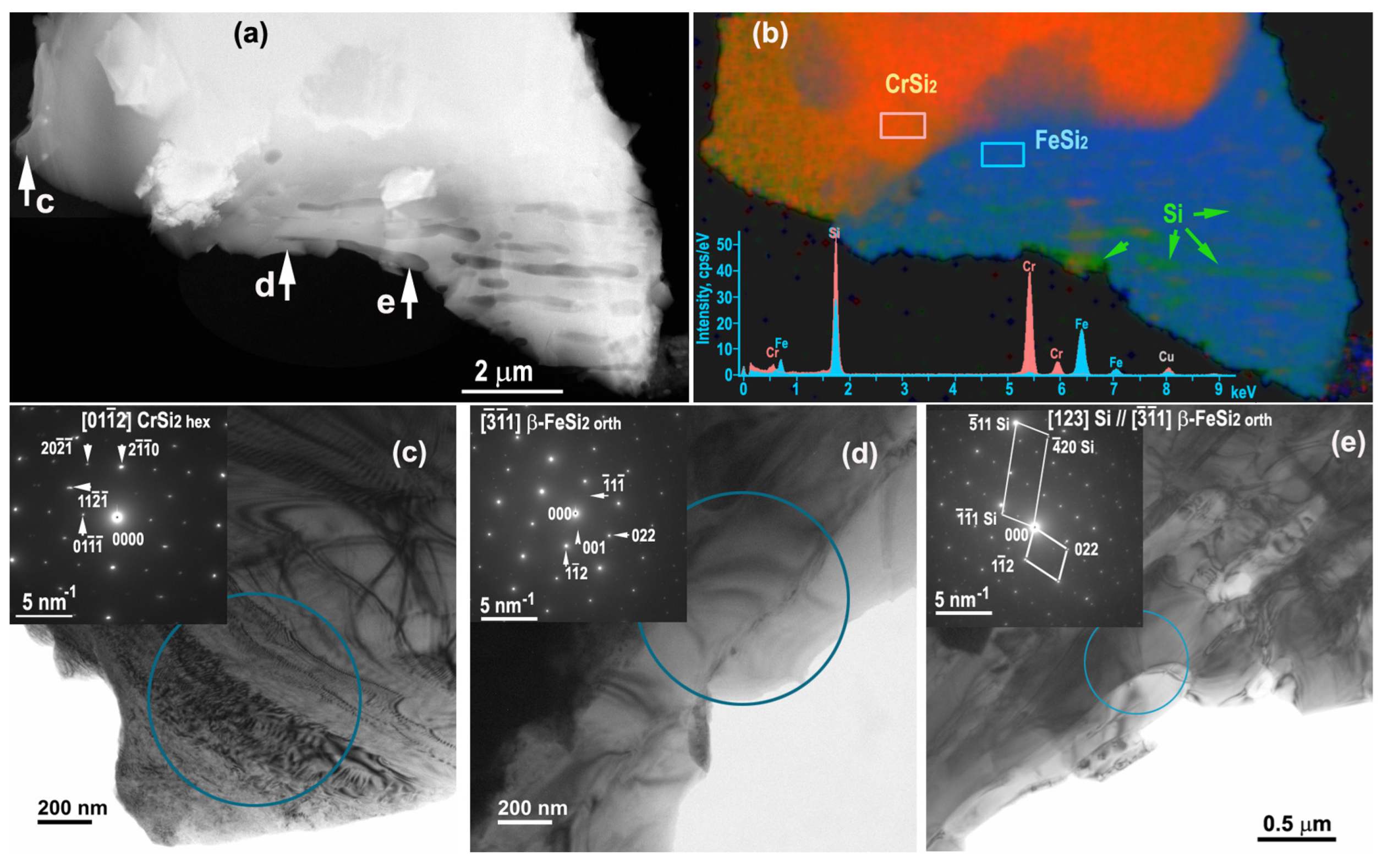
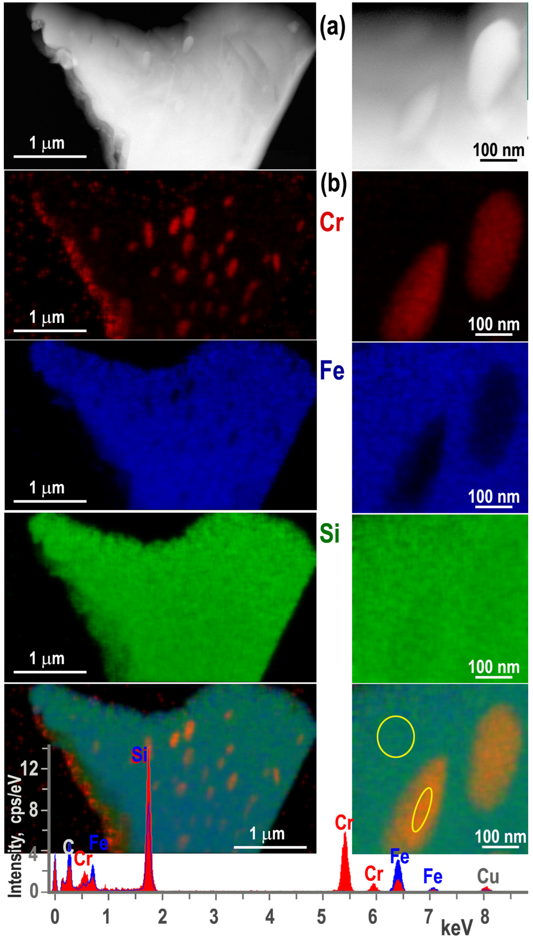
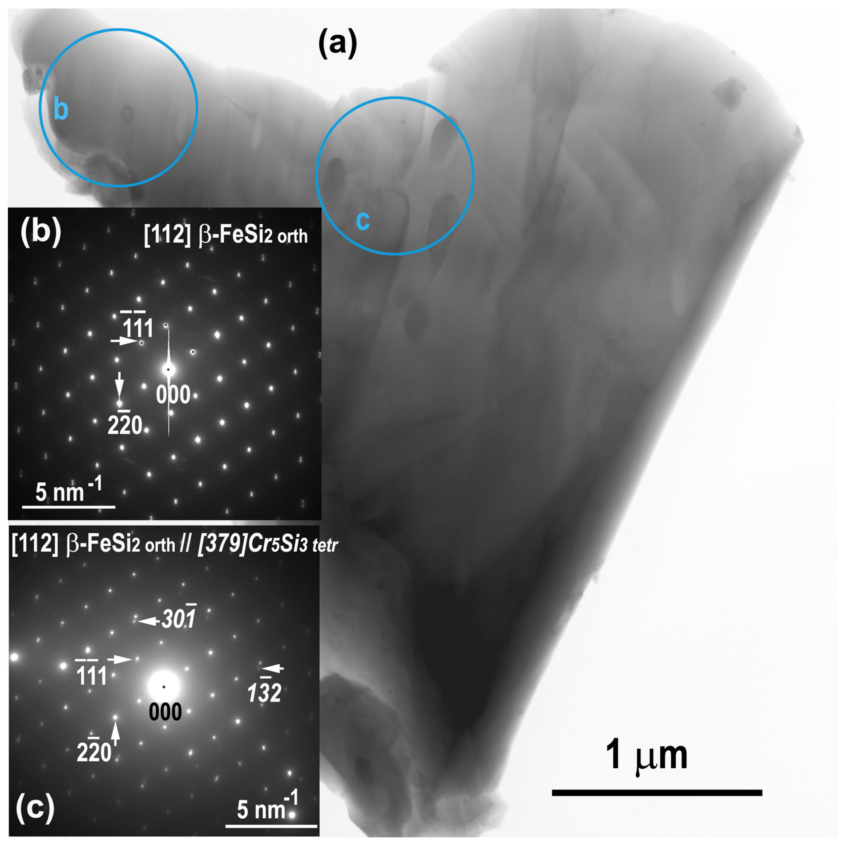
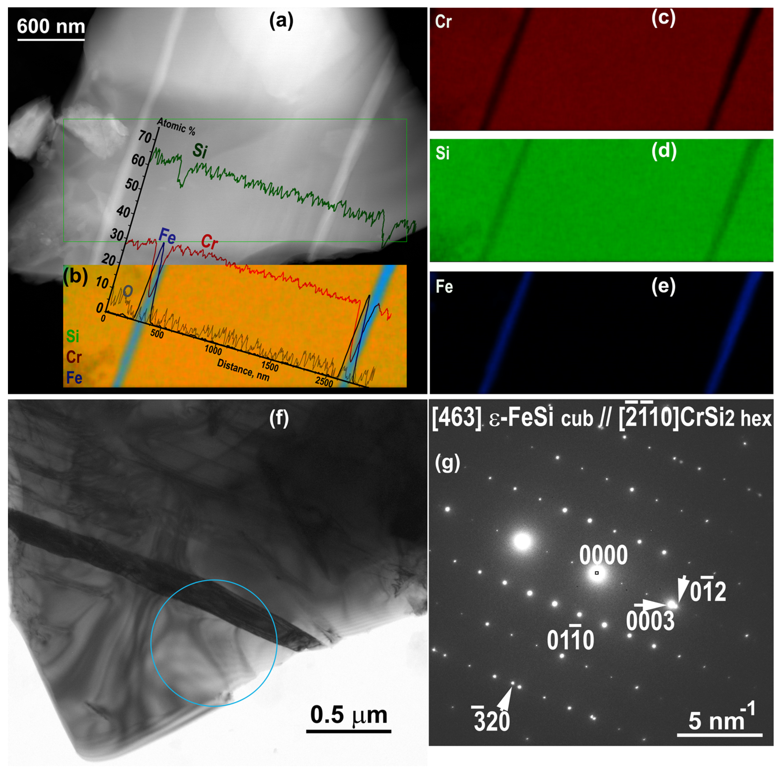
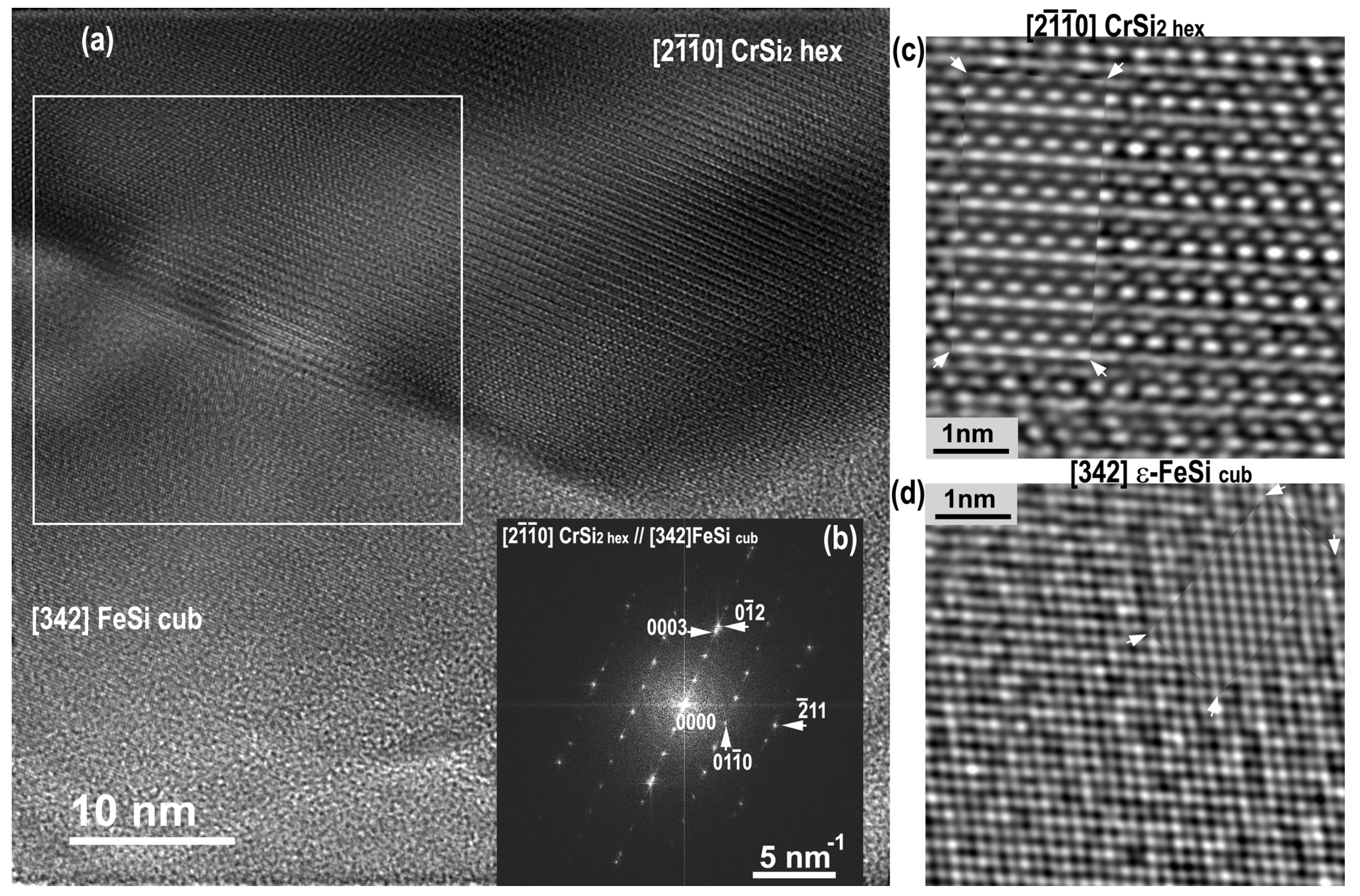
2.3. TEM, EDXS and Electron Diffraction Study

TEM images and the corresponding SAED patterns confirms the presence of the phase CrSi2 hex in both as grown (Figure 3a,b) and annealed samples (Figure 3d,e). However, quantitative EDXS microanalysis revealed a difference in iron impurity concentrations. It showed that CrSi2 grains in non-annealed samples contained about 1.5–2.0 at.% of Fe impurities while annealing results in their decrease by almost an order of magnitude to 0.2 at.%. The Fe−K line is clearly visible in the spectrum (Figure 3c) from as grown sample as contrast to the spectrum of the annealed sample (Figure 3f). The difference in Fe impurities content is highlighted in Figure 3g where counts cps/eV of the Cr-Kb lines have been normalized to the same level.
As-grown sample (non-annealed) contains the two Fe silicide phases: tetragonal α-FeSi2 and cubic ε−FeSi. Both phases participate in formation of a network spreading throughout the sample around large grains of Cr disilicide grains. Figure 4 shows TEM image, SAED patterns, and chemical spectra obtained from the α−FeSi2 and CrSi2 phases. Microanalysis of α-FeSi2 grains showed that they contained about 2 at.% Cr.
The TEM images and SAED patterns on Figure 5 are obtained from two adjacent areas. Diffraction patterns (Figure 5b,c) correspond to ε-FeSi grains seen respectively along the [122] and [124] directions. EDXS analysis show the presence of 10 at.% Cr in this area. The 3% lattice parameter difference between the ε-FeSi and CrSi, both with the space group P213 (Table 1), is a difference large enough that would have been observed in routine SAED interpretation if a mixture would have been present. BF TEM and HAADF STEM do not reveal any other kind of precipitates that are potentially Cr-rich. Therefore, one should consider that Cr has substituted to Fe in a (Fe−Cr)Si solid solution as reported by Wittmann et al. [41] and Gladyshevskii et al. [54] who reported a complete solubility between CrSi and ε-FeSi. Assuming a Vegard law, the FeSi lattice parameter would increase only by 0.3% for 10% Cr impurity, a change that will require special attention in further XRD and electron diffraction.
It was reported [55] that as a result of annealing of the Cr–Fe–Si ternary system in the range of 970–1190 K, eutectoid decomposition of tetragonal α−FeSi2 occurs with the formation of orthorhombic β–FeSi2 and silicon. Indeed, Si nanoprecipitates were revealed in β–FeSi2 (Figure 6). Two adjacent grains β–FeSi2 and CrSi2 are shown in HAADF STEM image (Figure 6a) and the corresponding element map (Figure 6b), which clearly demonstrates the phase boundary. Two superimposed EDXS spectra were taken from the selected rectangle rectangular areas shown on the map.
SAED patterns obtained from the circular areas indicated on the TEM images (Figure 6c–e) confirmed the phase composition of the grains − CrSi2 hex (area c), β−FeSi2 (area d), and elongated Si precipitates (area e). It was found that β−FeSi2 grain contains Si precipitates and about 2 at.% Cr impurities, while the CrSi2 grain contains about 0.2 at.% Fe.
In addition to Si nanoprecipitates, annealing of the samples leads to the formation of Cr−rich nanoparticles in the form of prolate spheroids in β-FeSi2 grains (Figure 7). From the phase distribution on EDXS maps, their larger length reaches up to 200 nm. The presence of these Cr rich silicide nanoparticles in the β−FeSi2 zones is in good agreement with the reduction of the Cr impurity in this phase from 2.0 at% to 0.3 at% after annealing. Quantitative EDXS analysis near the center of the larger ones leads to an apparent Cr−Si−Fe phase. Due to the relative size of the ellipsoids and a matrix thickness near 100 nm, they may be embedded in FeSi2 and the apparent concentration will be obtained that corresponds to a heterogeneous mixture of Cr−Si and FeSi2 phases.
BF TEM (Figure 8a) and electron diffraction patterns (Figure 8b,c) obtained from the selected circular areas “b” (without precipitates) and “c” (with Cr−rich precipitates) showed that the grain is a β−FeSi2, which contains Cr5Si3 tetr precipitates.
The presence of ε−FeSi lamellar precipitates of 100–150 nm wide inside the CrSi2 grains (Figure 9a–e) is unexpected. Its cubic structure was confirmed by electron diffraction (Figure 9f,g).
Nanoscale phase identification was carried out by HRTEM imaging and image simulation (Figure 10). The image simulation was performed using large ranges of sample thicknesses, defocus values, crystal orientations, and tilts [56,57]. The best agreement between experimental and simulations was obtained for thickness of about 90 nm and a defocus value close to that of Scherzer.
Electron diffraction patterns in Figure 6, Figure 8 and Figure 9 as well the Fourier diffractogram in Figure 10b allowed us to derive the crystallographic orientation relationships between phases what will be discussed later in the paper.

2.4. Crystallographic Orientation Relationships, Lattice Mismatch, Thermal Expansion Coefficient Mismatch

Interfaces control the mechanical, thermal, and electrical properties of polycrystalline and multiphase materials. Orientation relations between the phases show how well the atomic planes in two different phases fit together, which determines the nature of the interface (coherent, partly coherent, or incoherent). A partially coherent interface differs from a fully coherent interface only in that continuity interruptions occur due to the appearance of linear defects (dislocations) that compensate for the mismatch [58]. Only small (a few nm in size) precipitates can remain coherently strained up to a certain critical thickness or size.
The analysis of electron diffraction patterns where reflections from the adjacent phases are present allowed the determination of orientation relationships. Lattice mismatches at the interphase interfaces allow an evaluation of the strains. A complete analysis of the interface structure for all phases in this material, including the determination of the degree of boundaries coherence requires more work and will be the aim of future work.
The mismatch at interphase interfaces due to lattice mismatch and thermal expansion can generate mechanical stresses that can be relieved by the formation of defects including cracks and cavities. Thus, knowledge of the corresponding lattice interplanar spacings and thermal expansion coefficients (listed in Table 3) of materials is necessary to compare the relative contributions of strain induced by thermal expansion coefficient mismatch to strains from the crystal structure.
The in-plane strain between two adjacent phases is defined as
δ l a t t i c e = 2 | d F e d C r   o r   S i | d F e + d C r   o r   S i
where dFe and dCr or dSi are the interplanar spacings of the corresponding planes of Fe and Cr silicides or Si at their interfaces (the corresponding interplanar spacing values are listed in Table 3).
The following orientation relationships between phases are found:
1. [881] (1 1 ¯ 0) α−FeSi2 tetr // [11 2 ¯ 0] (2 2 ¯ 00) CrSi2 hex;
2. [ 7 ¯ 15 ¯   8] (713) β−FeSi2 orth // [2 1 ¯ 1 ¯ 0] (02 2 ¯ 4) CrSi2 hex;
3. [2 1 ¯ 1 ¯ 0] (0003) CrSi2 hex // [342] (0 1 ¯ 2) ε−FeSi cub;
4. [2 1 ¯ 1 ¯ 0] (0003) CrSi2 hex // [463] (0 1 ¯ 2) ε−FeSi cub;
5. [11 1 ¯ 0] (0003) CrSi2 hex // [120] ( 2 ¯ 10) ε−FeSi cub;
6. [112] ( 1 ¯ 5 ¯ 3) β−FeSi2 orth.// [379] (233) Cr5Si3 tetr;
7. [311] ( 2 ¯ 2 ¯ 8) β−FeSi2 orth.// [123] (60 2 ¯ ) Si cub;
Each from listed 7 orientations relationships have several variants that provide the same lattice mismatch.
The deformation caused by differences in thermal expansion of materials can be represented as [63]
δ t h e r m = δ t h e r m T δ t h e r m R T = d 1 R T ( α 1 α 2 ) Δ T d 2 R T ( 1 + α 2 Δ T ) ,
where δ t h e r m T and δ t h e r m R T are the in-plane strain at the annealing and room temperature, respectively; d 1 R T and d 2 R T are the corresponding interplanar spacings in the crystallographic lattices of different phases at room temperature, Δ T is the difference between the synthesis/annealing temperature and room temperature, α 1 and α 2 are the thermal expansion coefficients of phases in two adjacent grains 1 and 2. It is accepted that if materials have similar thermal expansion coefficients, room temperature lattice parameters of both materials at interfaces can be used [64].
The comparison of lattice and thermal expansion coefficient mismatches (Table 4) shows that the possible strains are mainly induced by the lattice mismatch of the adjacent phases, and the contribution of thermal expansion coefficient mismatches is insignificant.
The results show that the formation of the μm-size scaled ε-FeSi cub lamellas leads to a large lattice mismatch with the CrSi2 phase, and silicon crystallites have not only to a large lattice mismatch between with the β-FeSi2 tetr phase, but a noticeable misfit between their coefficients of thermal expansion. In fact, the material fracture occurs along the silicon crystallites and the interface with iron silicide what is clearly visible in Figure 6a,b,e. Thus, formation of large ε-FeSi cub lamellar precipitates and Si nanocrystals weakens the mechanical stability of the ternary allows, and cracking with crumbling of the samples both before and after annealing is a consequence of stress relaxation.

3. Materials and Methods

High-purity iron (99.5 wt.%, powder, Sigma-Aldrich, St. Louis, MI, USA), chromium (99.5 wt.%, powder, Sigma-Aldrich), and silicon (99.0 wt.%, powder, Sigma-Aldrich) were used as starting materials to prepare stoichiometric FeCrSi4. The powder mixture was melted in an arc melting furnace at T = 1723 K, and then then crystallized under vacuum (about 0.1 Pa). A part of the samples was finally annealed in air at T = 1073 K for 72 h.
X-ray powder diffraction (XRD) patterns were obtained in reflection mode using a Rigaku MiniFlex 600 diffractometer (Rigaku Corporation, Japan) with the CuKα radiation (45 kV, 40 mA, Ni–Kβ filter) in the angle range 2θ = 15°–100° with a scanning step of 0.02° and a rate of 1°/min. The quantitative ratio of the identified phases was estimated by the Rietveld method using PANalytical X’Pert High Score Plus software (Malvern Panalytical, UK). In the initial stages the overall zero error, phase scale factors, background, profile parameters, and lattice parameters of identified phases were refined. The peak shapes were approximated with pseudo-Voight profile function. Since the CrSi2 and FeSi2 phases exhibited the different pronounced orientations, the preferred texture parameters were also refined in the final stages.
To obtain an overview of the multiphase grain distribution and elemental composition, the mechanically polished samples were characterized using a scanning electron microscope (SEM, FEI Scios, Massachusetts, USA) at accelerating voltages between 5−15 keV) and equipped with an EDAX energy dispersive X-ray spectrometry (EDXS) system (Pleasanton, CA, USA) running under the TEAM™ EDS Software Suite and fitted with an Apollo X Silicon Drift Detector.
Thin samples for TEM (transmission electron microscopy) were prepared using conventional Ar ion milling (Gatan PIPS, Pleasanton, CA, USA) at room temperature after preliminary mechanical polishing. This preparation method was chosen because the samples were found to be quite fragile and easily broken at thin places, as well as because the useful areas were larger.
TEM, high resolution TEM (HRTEM), bright field (BF), and high angular annular dark field (HAADF) scanning TEM (STEM) images, EDXS microanalysis, and selected area electron diffraction (SAED) patterns were obtained at a 200 kV accelerating voltage on an Tecnai Osiris analytical field emission transmission electron microscope (FEI, Hillsboro, OR, USA) fitted with a 4 SDD detectors Super X ChemiSTEM EDXS system (FEI) running under ESPRIT software (Bruker, Ratingen, Germany).
Element quantification from EDXS was performed with the Cliff–Lorimer ratio method [65] in TEM and ZAF (Z = Atomic number, A = Self-absorption, F = Fluorescence) method [66,67] in SEM. Low concentrations of oxygen and aluminum impurities were ignored when writing the stoichiometries.
Crystallographic phase analysis was performed using the selected area electron diffraction (SAED) patterns and Fourier transform diffractograms (FFT) of high-resolution TEM (HRTEM) images, which were processed with the DigitalMicrograph suite GMS 2.31 (Gatan Inc, Pleasanton, CA, USA). SAED patterns and FFT were interpreted with the JEMS software [68].

4. Discussion and Conclusions

Binary Cr and Fe disilicides were found in the sample obtained by high-temperature reaction at 1723 K and after annealing at 1073 K for 3 days. Neither ternary silicides, nor brittle σ−Cr−Fe phase were observed.
Low solubility of Fe dicilides was observed in CrSi2 in both as-grown and annealed samples which allows for the formation of large (200–300 μm size) homogeneous CrSi2 grains. While α−, β−FeSi2 regions have significantly smaller grain sizes.
The ε−FeSi phase is present in both as grown and annealed samples. In the annealed material it forms lamellar precipitates of about 100–150 nm in width.
The CrSi2 grains contain Fe impurities at a concentration between 1.5 at.% and 2.0 at.% (mainly before annealing) and annealing reduce it to 0.2%. The FeSi2 grains also contain Cr impurities of about 2 at. %. Up to 10 atomic % Cr was detected in the cubic ε−FeSi phase.
Annealing leads to the formation of Si and Cr5Si3 precipitates and a significant decrease in the Cr concentration in the FeSi2 regions where Cr5Si3 precipitates appeared.
XRD showed that the amount of the CrSi2 phase was approximately 50 % before and after annealing, while the amount of ε−FeSi phase decreased after annealing from 7.5 to about 1.3 w.%. This fact may mean that part of the ε−FeSi phase was taken together with α-FeSi2 for the phase transformation to create the β−FeSi2 phase.
Secondary phases like ε−FeSi and particularly Si have a large lattice mismatch with Cr and Fe dicilicides which consequently leads to stresses and strains and eventually to cracking of the material. In comparison, the thermal expansion coefficient has only a minor effect.

Future Research Directions

Investigations of chemistry, crystallography, and properties of Cr and Fe silicides have a long and rich history. Low cost, abundance, and ecological safety are the most attractive features of this type of compounds for their use in mass production. However, “the characterization and understanding of single-metal silicides is only a first step”, and “a full knowledge of individual binary systems is insufficient to analyze the product phases since the growth of a ternary compound may now be part of the evolution of the structures” [69].
In fact, the ternary Cr−Fe−Si system is a complex system not only because of the multiphase composition, but also because of the complex spatial arrangement of the various phases and their mutual distribution in bulk materials. How it was noticed in [70] that there are extensive solid solutions in the ternary system, but there is no formation of ternary compound phase in the Fe−Si−Cr system.
Therefore, we consider that more research is still needed to achieve optimal composition among several different binary and ternary (if any) phases and processing to develop the adequate microstructure. First, studying the structure at the nano- and atomic level will help to improve knowledge about the mechanism of phases and interphase interfaces formation and stability, chemical bonding, and diffusion kinetics. We must emphasize that for this goal, a combination of several methods is needed, such as XRD, electron diffraction, analytical SEM and TEM, including high resolution (S)TEM, to gain a clear understanding of multiphase systems for better control of synthesis.

Author Contributions

Conceptualization, E.I.S. and F.Y.S.; data curation, E.I.S. and F.Y.S.; investigation, E.I.S., N.A.A. and A.G.I.; resources, F.Y.S.; writing—original draft preparation, E.I.S., F.Y.S. and A.G.I.; writing—review and editing, E.I.S. and P.A.B. All authors have read and agreed to the published version of the manuscript.

Funding

This research was supported by the Ministry of Science and Higher Education of the Russian Federation.

Data Availability Statement

Data are available at reasonable request from the authors.

Acknowledgments

This work was carried out using the equipment of the Shared Research Centers of A.V. Shubnikov Institute of Crystallography, FSRC “Crystallography and Photonics”.

Conflicts of Interest

The authors declare no conflict of interest.

References

  1. Yamamoto, K.; Kimura, Y.; Mishima, Y. Phase constitution and microstructure of the Fe-Si-Cr ternary ferritic alloys. Scr. Mater. 2004, 50, 977–981. [Google Scholar] [CrossRef]
  2. Han, H.K.; Loka, C.; Yang, Y.M.; Kim, J.H.; Moon, S.W.; Cho, J.S.; Lee, K.-S. High capacity retention Si/silicide nanocomposite anode materials fabricated by high-energy mechanical milling for lithium-ion rechargeable batteries. J. Power Sources 2015, 281, 293–300. [Google Scholar] [CrossRef]
  3. Min, E.H.; Kim, M.S.; Koh, J.G. Study of an Electromagnetic Wave Absorber Prepared with Fe-Si-Cr for Mobile Phones. J. Korean Phys. Soc. 2008, 53, 2086–2089. [Google Scholar] [CrossRef]
  4. Han, H.; Pan, D.; Li, D. Study on Fe-Si-Cr Soft magnetic composite coated with silicon dioxide. Mater. Res. Express 2019, 6, 026104. [Google Scholar] [CrossRef]
  5. Kim, S.W.; Cho, M.K.; Mishima, Y.; Choi, D.C. High temperature thermoelectric properties of p- and n-type β-FeSi2 with some dopants. Intermetallics 2003, 11, 399–405. [Google Scholar] [CrossRef]
  6. Isoda, Y.; Udono, H. Preparation and Thermoelectric Properties of Iron Disilicide. In Thermoelectrics and Its Energy Harvesting Materials, Preparation, and Characterization in Thermoelectrics; Rowe, D.M., Ed.; CRS Press; Taylor & Francis Group: Boca Raton, FL, USA, 2012; pp. 18-1–18-25. [Google Scholar]
  7. Nishida, I. The crystal growth and thermoelectric properties of chromium disilicide. J. Mater. Sci. 1972, 7, 1119–1124. [Google Scholar] [CrossRef]
  8. Khalil, M.; Moll, A.; Godfroy, M.; Letrouit-Lebranchu, A.; Villeroy, B.; Alleno, E.; Viennois, R.; Beaudhuin, M. Thermoelectric properties and stability of nanostructured chromium disilicide CrSi2. J. Appl. Phys. 2019, 126, 135103. [Google Scholar] [CrossRef]
  9. Chen, G.; Dresselhaus, M.S.; Dresselhaus, G.; Fleurial, J.-P.; Caillat, T. Recent developments in thermoelectric materials. Int. Mater. Rev. 2003, 48, 45–66. [Google Scholar] [CrossRef]
  10. Popescu, A.; Haney, P.M. Interface scattering in polycrystalline thermoelectrics. J. Appl. Phys. 2014, 115, 123701. [Google Scholar] [CrossRef]
  11. Chart, T.; Putland, F.; Dinsdale, A. Calculated phase equilibria for the Cr-Fe-Ni-Si system—I ternary equilibria. CALPHAD 1980, 4, 27–46. [Google Scholar] [CrossRef]
  12. Lindholm, M. A Thermodynamic description of the Fe-Cr-Si system with emphasis on the equilibria of the sigma (σ) phase. J. Phase Equilibria 1997, 18, 432–440. [Google Scholar] [CrossRef]
  13. Raghavan, V. Cr-Fe-Si (Chromium-Iron-Silicon). J. Phase Equilibria Diffus. 2004, 25, 545–546. [Google Scholar] [CrossRef]
  14. Wen, A.; Zhang, L.; Liu, L.; Masset, P.J.; Zhao, Y.; Zheng, L.; Zhao, F. Experimental Investigation of Phase Equilibria in the Fe-Cr-Si. J. Phase Equilibria Diffus. 2020, 41, 587–597. [Google Scholar] [CrossRef]
  15. Murarka, S.P. Transition metal silicides. Ann. Rev. Mater. Sci. 1983, 13, 117–137. [Google Scholar] [CrossRef]
  16. Nicolet, M.-A.; Lau, S.S. Formation and Characterization of Transition-Metal Silicides. In Materials and Process Characterization; Einspruch, N.G., Larrabee, G.B., Eds.; VLSI Electronics Microstructure Science; Elsevier: Amsterdam, The Netherlands, 1983; Volume 6, pp. 329–464. [Google Scholar]
  17. D’Heurle, F.; Gas, P. Kinetics of formation of silicides: A review. J. Mater. Res. 1986, 1, 205–221. [Google Scholar] [CrossRef]
  18. Burkov, A.T. Silicide Thermoelectrics: Materials for Energy Harvesting. Phys. Status Solidi A 2018, 215, 1800105. [Google Scholar] [CrossRef]
  19. Pshenay-Severin, D.A.; Burkov, A.T. Electronic structure of B20 (FeSi-Type) transition-metal monosilicides. Materials 2019, 12, 2710. [Google Scholar] [CrossRef]
  20. Ferrer-Argemi, L.; Yu, Z.; Lee, J. Effects of metal silicide inclusion interface and shape on thermal transport in silicon nanocomposites. J. Appl. Phys. 2019, 126, 035106. [Google Scholar] [CrossRef]
  21. Singh, S.; Sharma, Y.C. A review on silicide based materials for thermoelectric applications. IJAERS 2021, 8, 160–168. [Google Scholar] [CrossRef]
  22. Abbassi, L.; Mesguich, D.; Berthebaud, D.; Le Tonquesse, S.; Srinivasan, B.; Mo-ri, T.; Coulomb, L.; Chevallier, G.; Estournès, C.; Flahaut, E.; et al. Effect of Nanostructuring on the Thermoelectric Properties of β-FeSi2. Nanomaterials 2021, 11, 2852. [Google Scholar] [CrossRef]
  23. Tarani, E.; Stathokostopoulos, D.; Tsipas, S.A.; Chrissafis, K.; Vourlias, G. Effect of the Deposition Time and Heating Temperature on the Structure of Chromium Sili-cides Synthesized by Pack Cementation Process. Corros. Mater. Degrad. 2021, 2, 12. [Google Scholar] [CrossRef]
  24. Lue, J.-T.; Mu, S.-J. Ellipsometry and structure studies of chromium, molybdenum, and platinum silicides. Phys. Rev. B 1987, 36, 1657–1661. [Google Scholar] [CrossRef] [PubMed]
  25. Bedeker, C.J.; Kritzinger, S.; Lombaard, J.C. Formation and microstructure of various thin film chromium silicide phases. Thin Solid Films 1986, 141, 117–127. [Google Scholar] [CrossRef]
  26. Otogawaa, N.; Wanga, S.; Kihara, S.; Liub, Z.; Fukuzawa, Y.; Suzuki, Y.; Osamura, M.; Ootsuka, T.; Miyake, T.; Nakayama, Y.; et al. Semiconductor–metal phase transition of iron disilicide by laser annealing and its application to form device electrodes. Thin Solid Films 2004, 461, 223–226. [Google Scholar] [CrossRef]
  27. Liang, S.; Islam, R.; Smith, D.J.; Bennett, P.A. Phase transformation in FeSi2 nanowires. J. Cryst. Growth 2006, 295, 166–171. [Google Scholar] [CrossRef]
  28. Igarashi, S.; Haraguchi, M.; Aihara, J.; Saito, T.; Yamaguchi, K.; Yamamoto, H.; Hojou, K. Observation of iron silicide formation by plan-view transmission electron microscopy. J. Electron Microsc. 2004, 53, 223–228. [Google Scholar] [CrossRef]
  29. Moll, A.; Hermet, P.; Bantignies, J.-L.; Candolfi, C.; Lenoir, B.; Maurin, D.; Ra-monda, M.; Oliviero, E.; Fréty, N. Influence of nanostructurationonthe vibrational, electronic and optical properties of CrSi2 thin films. J. Phys. Chem. C 2020, 124, 28267–28276. [Google Scholar] [CrossRef]
  30. Schuette, M.; Wartchow, R.; Binnewies, M. Shape controlling synthesis—Formation of Fe3Si by the reaction of iron with silicon tetrachloride and crystal structure refinement. ZAAC 2003, 629, 1846–1850. [Google Scholar] [CrossRef]
  31. Joergensen, J.E.; Rasmussen, S.E. A neutron diffraction study of Cr3Si. Acta Cryst. B 1982, 38, 346–347. [Google Scholar] [CrossRef]
  32. Buschow, K.H.J.; van Engen, P.G.; Jongebreur, R. Magneto-optical properties of metallic ferromagnetic materials. J. Magn. Magn. Mater. 1983, 38, 1–22. [Google Scholar] [CrossRef]
  33. Goldschmidt, H.J.; Brand, J.A. The constitution of the chromium-niobium-silicon system. J. Less-Common Met. 1961, 3, 34–43. [Google Scholar] [CrossRef]
  34. Weill, A.R. Structure of the Eta Phase of the Iron-Silicon System. Nature 1943, 152, 413. [Google Scholar] [CrossRef]
  35. Dauben, C.H.; Templeton, D.H.; Myers, C.E. The crystal structure of Cr5Si3. J. Phys. Chem. 1956, 60, 443–445. [Google Scholar] [CrossRef]
  36. Aronsson, B. An investigation of the Me5Si3-MeSi region of the Mn-Fe-Si and some related systems. Acta Chem. Scand. 1958, 12, 308–313. [Google Scholar] [CrossRef]
  37. Brukl, C.; Nowotny, H.; Benesovsky, F. Untersuchungen in den Dreistoffsystemen: V-Al-Si, Nb-Al -Si, Cr-Al-Si, Mo-Al-Si bzw. Cr(Mo)-Al-Si. Mon. Chem. 1961, 92, 967–980. [Google Scholar] [CrossRef]
  38. Johnson, V.; Weiher, J.F.; Frederick, C.G.; Rogers, D.B. Magnetic and Moessbauer effect studies of Mn5Si3:Fe5Si3 solid solutions. J. Solid State Chem. 1972, 4, 311–323. [Google Scholar] [CrossRef]
  39. Vočadlo, L.; Knight, K.S.; Price, G.D.; Wood, I.G. Thermal expansion and crystal structure of FeSi between 4 and 1173 K determined by time-of-flight neutron powder diffraction. Phys. Chem. Miner. 2002, 29, 132–139. [Google Scholar] [CrossRef]
  40. Pauling, L.; Soldate, A.M. The nature of the bonds in the iron silicide FeSi and related crystals. Acta Cryst. 1948, 1, 212–216. [Google Scholar] [CrossRef]
  41. Dusausoy, Y.; Protas, J. Structure cristalline du disilicure de fer, FeSi2 beta. Acta Cryst. B 1971, 27, 1209–1218. [Google Scholar] [CrossRef]
  42. Nishida, I.; Sakata, T. Semiconducting properties of pure and Mn-doped chromium disilicides. J. Phys. Chem. Solids 1978, 39, 499–505. [Google Scholar] [CrossRef]
  43. Yamane, H.; Yamada, T. Effects of stacking fault on the diffraction intensities of beta-(FeSi2). J. Alloys Compd. 2009, 476, 282–287. [Google Scholar] [CrossRef]
  44. Zelenin, L.P.; Radovskii, I.Z.; Sidorenko, F.A.; Gel’d, P.V.; Rabinovich, B.S. Structural characteristics of solid solutions of chromium disilicide with vanadium and titanium disilicides. Powder Metall. Met. Ceram. 1966, 5, 896–900. [Google Scholar] [CrossRef]
  45. Mason, K.; Mueller-Vogt, G. Osmium disilicide: Preparation, crystal growth, and physical properties of a new semiconducting compound. J. Cryst. Growth 1983, 63, 34–38. [Google Scholar] [CrossRef]
  46. Tanaka, K.; Nawata, K.; Inui, H.; Yamaguchi, M.; Koiwa, M. Refinement of crystallographic parameters in refractory metal disilicides. MRS Online Proc. Libr. (OPL) 2001, 646, N4.3.1–N4.3.5. [Google Scholar] [CrossRef]
  47. Li, G.; Nicheng, S.; Ming, X.; Zhesheng, M.; Wenji, B.; Qingsong, F. X-ray diffraction investigation of native Si-Fe alloy minerals from Luobusha, Tibet. Front. Earth Sci. China 2007, 1, 21–25. [Google Scholar] [CrossRef]
  48. Bond, W.L.; Kaiser, W. Interstitial versus substitutional oxygen in silicon. J. Phys. Chem. Solids 1960, 16, 44–45. [Google Scholar] [CrossRef]
  49. Wittmann, A.; Burger, K.O.; Nowotny, H. Untersuchungen im Dreistoff: Ni-Al-Si sowie von Mono- und Disilicidsystemen einiger Uebergangsmetalle. Mon. Chem. 1962, 93, 674–680. [Google Scholar] [CrossRef]
  50. Straumanis, M.E.; Aka, E.Z. Lattice parameters, coefficients of thermal expansion and atomic weights of purest silicon and germanium. J. Appl. Phys. 1952, 23, 330–334. [Google Scholar] [CrossRef]
  51. Robinson, V.N.E. Imaging with backscattered electrons in a scanning electron microscope. Scanning 1980, 3, 15–26. [Google Scholar] [CrossRef]
  52. Lloyd, G.E. Atomic number and crystallographic contrast images with the SEM: A review of backscattered electron techniques. Mineral. Mag. 1987, 51, 3–19. [Google Scholar] [CrossRef] [Green Version]
  53. Goldstein, J.I.; Newbury, D.E.; Michael, J.R.; Ritchie, N.W.M.; Scott, J.H.J.; Joy, D.C. Backscattered Electrons. In Scanning Electron Microscopy and X-ray Microanalysis; Goldstein, J.I., Newbury, D.E., Michael, J.R., Ritchie, N.W.M., Scott, J.H.J., Joy, D.C., Eds.; Springer: New York, NY, USA, 2017; pp. 15–28. [Google Scholar]
  54. Gladyshevskii, E.I. Crystal structure of compounds and phase equilibria in ternary systems of two transition metals and silicon. Powder Metall. Met. Ceram. 1962, 1, 262–265. [Google Scholar] [CrossRef]
  55. Vecherskii, S.I.; Sidorenko, F.A. Effect of phase transformation in higher iron silicide on the electrical conductivity of the multiphase system iron silicide-glass. II. Effect of structural transformation in lebeauite on the temperature dependence for composite resistivity. Sov. Powder Metall. Met. Ceram. 1992, 31, 835–838. [Google Scholar] [CrossRef]
  56. Stadelmann, P.A. EMS—A software package for electron diffraction analysis and HREM image simulation in materials science. Ultramicroscopy 1987, 21, 131–146. [Google Scholar] [CrossRef]
  57. Imamov, R.M.; Klechkovskaya, V.V.; Suvorova, E.I. High-Resolution Transmission Electron Microscopy for Crystallographic Study of Nanomaterials. Crystallogr. Rep. 2011, 56, 650–661. [Google Scholar] [CrossRef]
  58. Howe, J.M.; Aaronson, H.I.; Hirth, J.P. Aspects of interphase boundary structure in diffusional phase transformations. Acta Mater. 2000, 48, 3977–3984. [Google Scholar] [CrossRef]
  59. Rabinovich, B.S.; Radovskii, I.Z.; Gel’d, P.V. Coefficients of thermal expansion of chromium disilicide and its solid solutions with TiSi2 and VSi2. Sov. Powder Metall. Met. Ceram. 1968, 7, 879–883. [Google Scholar] [CrossRef]
  60. Imai, M.; Isoda, Y.; Udono, H. Thermal expansion of semiconducting silicides β-FeSi2 and Mg2Si. Intermetallics 2015, 67, 75–80. [Google Scholar] [CrossRef]
  61. Krentsis, R.P.; Kalishevich, G.I.; Gel’d, P.V.; Andreeva, L.P. Thermal expansion of monosilicides of chromium, manganese, iron, and cobalt. Sov. Phys. J. Vol. 1972, 15, 143–145. [Google Scholar] [CrossRef]
  62. Mazur, A.V.; Gasik, M.M. Thermal expansion of silicon at temperatures up to 1100 °C. J. Mater. Process. Tech. 2009, 209, 723–727. [Google Scholar] [CrossRef]
  63. Kladko, V.; Kuchuk, A.; Lytvyn, P.; Yefanov, O.; Safriuk, N.; Belyaev, A.; Mazur, Y.I.; DeCuir, E.A., Jr.; Ware, M.E.; Salamo, G.J. Substrate effects on the strain relaxation in GaN/AlN short-period superlattices. Nanoscale Res. Lett. 2012, 7, 289. [Google Scholar] [CrossRef] [Green Version]
  64. Liu, H.; Cheng, X.; Valanoor, N. A universal approach for predicting crystallography of heterogeneous epitaxial nanocrystals with multiple orientation relationships. ACS Appl. Mater. Interfaces 2016, 8, 34844–34853. [Google Scholar] [CrossRef] [PubMed]
  65. Hoeft, H.; Schwaab, P. Investigations towards optimizing EDS analysis by the Cliff-Lorimer method in scanning transmission electron microscopy. X-ray Spectrom. 1988, 17, 201–208. [Google Scholar] [CrossRef]
  66. Yakowitz, H. Methods of quantitative analysis. In Practical Scanning Electron Microscopy; Goldstein, J.I., Yakowitz, H., Newbury, D.E., Lifshin, E., Colby, J.W., Coleman, J.R., Eds.; Plenum Press: New York, NY, USA, 1975; pp. 327–332. [Google Scholar]
  67. Newbury, D.E.; Ritchie, N.W.M. Electron-Excited X-ray Microanalysis by Energy Dispersive Spectrometry at 50: Analytical Accuracy, Precision, Trace Sensitivity, and Quantitative Compositional Mapping. Microsc. Microanal. 2019, 25, 1075–1105. [Google Scholar] [CrossRef] [PubMed]
  68. Stadelmann, P. JEMS. 2021. Available online: https://www.jems-swiss.ch/ (accessed on 19 January 2023).
  69. Setton, M.; van der Spiegel, J. Silicide formation from ternary metal-metal-silicon systems. Thin Solid Film. 1988, 156, 351–363. [Google Scholar] [CrossRef]
  70. Cui, S.; Jung, I.-H. Thermodynamic assessments of the Fe-Si-Cr and Fe-Si-Mg systems. Metall. Mater. Trans. A 2017, 48, 4342–4355. [Google Scholar] [CrossRef]
Figure 1. Phase analysis using Rietveld refinement for the Fe−Cr−Si samples before (a) and after annealing (b). The Bragg peaks of α−FeSi2 tetr and β−FeSi2 orth, ε−FeSi and Si cub were labeled with 3 indices, and the planes in hexagonal CrSi2 are shown with the Miller-Bravais indices (hkil), labels of visible Si (111, 022 and 113) peaks are shown under the XRD pattern.
Inorganics 11 00073 g001
Figure 2. Non-annealed sample: BSE SEM image with grains of different chemical composition (based on EDXS analysis) CrSi2, CrFe1.5Si4 and CrFe3Si5 and thus responsible for the 3 different brightness levels (a); enlarged area of the selected rectangular area corresponding to an apparent chemical composition CrFe1.5Si4 (b); BSE intensity line profile through grains of different effective atomic numbers due to their specific compositions (c), corresponding EDXS map with a mixture of Cr and Fe silicides that satisfies microanalysis data and BSE Z-contrast (d).
Inorganics 11 00073 g002
Figure 3. Comparison of CrSi2 grain in non−annealed (left) and annealed (right) samples. TEM image (a) with the corresponding SAED pattern obtained along the [4 2 ¯ 2 ¯ 3] CrSi2 hex direction (b), EDXS spectrum with Fe−Kα peak visible (c). CrSi2 grain in annealed sample (right): TEM image (d) with the corresponding SAED pattern obtained along the [11 2 ¯ 3] CrSi2 hex direction (e); EDXS spectrum with Fe−Kα peak absent (f); Superimposed EDXS spectra of CrSi2 from non-annealed (light blue) and annealed samples (dark blue) after Cr−Kβ intensity normalization to highlight the loss of Fe in the CrSi2 phase after annealing (g).
Inorganics 11 00073 g003
Figure 4. Non-annealed sample: TEM image with α-FeSi2 and CrSi2 hex phases (a), the corresponding SAED patterns obtained from α−FeSi2 [110] (b) and [11 2 ¯ 9] CrSi2 directions (c); spectra obtained from the α-FeSi2 (d) and CrSi2 areas showed all elements (e).
Inorganics 11 00073 g004
Figure 5. Non-annealed sample: FeSi grains from the network from. EDXS elemental map (containing about 10 at% Cr) with the spectrum (ad), TEM image and the corresponding SAED patterns taken from the left and right grains along the [124] ε−FeSi and the [122] ε−FeSi directions.
Inorganics 11 00073 g005
Figure 6. Annealed sample: HAADF STEM image (a) and EDXS map (in atomic %) showing grains CrSi2 and FeSi2 with Si precipitates (b); TEM images (ce) with the corresponding SAED patterns taken from [01 1 ¯ 2] CrSi2 hex, [ 3 ¯ 3 ¯ 1] β−FeSi2 orth and [ 3 ¯ 3 ¯ 1] β−FeSi2 orth with Si precipitates along the [123] direction.
Inorganics 11 00073 g006
Figure 7. Grain of Fe disilicide and Cr-rich particles in annealed sample. Left column: HAADF STEM image (a), element maps from Cr, Fe and Si (b). Right column: enlarged HAADF STEM image and the elemental maps; superimposed element maps and spectra obtained from the FeSi2 grain and Cr−rich nanoparticle (selected areas).
Inorganics 11 00073 g007
Figure 8. Annealed sample: BF STEM image (a); SAED pattern obtained from the [112] β−FeSi2 orth directions (b); SAED pattern obtained from the β−FeSi2 orth along the [112] direction and Cr5Si3 nanoprecipitates along the [379] direction (Miller indexes are in regular or italic characters for FeSi2 Cr5Si3, respectively (c).
Inorganics 11 00073 g008
Figure 9. Annealed sample: HAADF STEM image (a) the EDXS map (in atomic %) and inserted concentration profiles from Cr, Si and Fe across the across the lamellar precipitate (b), EDXS elemental maps from Cr (c), Si (d) and Fe (e); TEM image (f) and the SAED pattern (g) corresponding to the circular area in (f) [463] (012) ε−FeSi cub and [ 2 ¯ 1 ¯ 10] (0003) CrSi2 hex are parallel.
Inorganics 11 00073 g009
Figure 10. Annealed sample: HRTEM image taken at the interface FeSi cub / CrSi2 hex (a), Fourier diffractogram obtained from the selected rectangular area brings their zone axis [2 1 ¯ 1 ¯ 0] and [342], respectively (b); filtered HRTEM images from the [2 1 ¯ 1 ¯ 0] CrSi2 hex and [342] FeSi cub. HRTEM insets delimited by arrows are simulated HRTEM images using JEMS (c,d).
Inorganics 11 00073 g010
Table 1. Chemical and phase composition of binary Fe and Cr silicides.
Fe–SiCr–Si
PhaseSpace Group; Lattice Parameters (nm)# ICSDPhaseSpace Group; Lattice Parameters (nm)# ICSD
Fe3SiFm 3 ¯ m; a = 0.5665 [30];412838Cr3SiPm 3 ¯ n; a = 0.45599 [31];32509
Fm 3 ¯ m; a = 0.5662 [32].633537Pm 3 ¯ n; a = 0.4539 [33].199130
Fe5Si3P63/mcm; a = 0.67552, c = 0.47174 [34];42585Cr5Si3I4/mcm; a = 0.917, c = 0.4636 [35];15683
P63/mcm; a = 0.6755, c = 0.4715 [36];633525I4/mcm; a = 0.915, c = 0.464 [37].626782
P63/mcm; a = 0.6756, c = 0.4718 [38].633540
ε-FeSiP213; a= 0.445507 [39];5250CrSiP213; a = 0.4629 [33].626772
P213; a= 0.4489 [40];76945
β-FeSi2Cmca, a= 0.9863, b = 0.7791, c = 0.7833 [41];9119CrSi2P6222; a = 0.4428, c = 0.6364 [42]; 626776
Cmca, a= 0.9876, b = 0.7798, c = 0.7836 [43];163384P6222; a = 0.4428, c = 0.6364 [44];626787
Cmca, a= 0.988, b = 0.7798, c = 0.7839 [45].603890P6422; a = 0.4283, c = 0.6368 [46];96026
α-FeSi2P4/mmm, a = 0.2725, c = 0.5202 [47];5258SiFd 3 ¯ m, a = 0.54307 [48];29287
P4/mmm, a = 0.269, c = 0.5133 [49].633544Fd 3 ¯ m, a = 0.543086 [50].76268
Table 2. Phase composition of the samples according to the Rietveld refinement.
As Grown (Non-Annealed)Annealed
Rwp = 13.4%, GOF = 6.4Rwp = 11.5%, GOF = 5.2
phaseweight %Phaseweight %
CrSi250.5 (4)CrSi250.7 (3)
α−FeSi241.9 (4)β−FeSi246.8 (3)
ε−FeSi7.5 (2)ε−FeSi1.3 (1)
SiNot foundSi1.2 (1)
Table 3. Planes and corresponding interplanar spacings d, thermal expansion coefficients [23,59,60,61,62] to derive the lattice mismatch from orientation relationships.
Materialhkld, nmα·10−6 K−1
CrSi2 hex(2 2 ¯ 00)
(02 2 ¯ 4)
(0003)
0.19148
0.1222
0.2117
12.87
α–FeSi2 tetr(1 1 ¯ 0)0.1905712.0
β–FeSi2 orth(713)
( 1 ¯ 5 ¯ 3)
( 2 ¯ 2 ¯ 8)
0.12246
0.13259
0.09325
11.8
ε–FeSi cub(0 1 ¯ 2)
( 2 ¯ 10)
0.20351
0.20351
15.5
Cr5Si3 tetr(233)0.1320714.07
Si cub(60 2 ¯ ) 0.086174.3
Table 4. The thermal expansion coefficient misfit and lattice mismatch at the interphase interfaces.
InterfacesMisfit, δ thermMismatch, δ lattice
CrSi2 hex–α-FeSi2 tetr0–2.9·10−2%0.5%
CrSi2 hex–β-FeSi2 tetr7.8·10−2%0.2%
CrSi2 hex–ε-FeSi cub0.2%4.1%
β-FeSi2 tetr–Cr5Si3 tetr0.2%0.4%
β-FeSi2 tetr–Si cub0.6%7.9%
Disclaimer/Publisher’s Note: The statements, opinions and data contained in all publications are solely those of the individual author(s) and contributor(s) and not of MDPI and/or the editor(s). MDPI and/or the editor(s) disclaim responsibility for any injury to people or property resulting from any ideas, methods, instructions or products referred to in the content.

