Article

Microstructural Investigations of VO2 Thermochromic Thin Films Grown by Pulsed Laser Deposition for Smart Windows Applications

1
Department of Mechanical and Structural Engineering and Materials Science, University of Stavanger, N-4036 Stavanger, Norway
2
National Institute of Materials Physics, Atomistilor 405A, RO 077125 Magurele, Romania
3
National Institute for Laser, Plasma and Radiation Physics, Atomistilor 409, RO 077125 Magurele, Romania
*
Author to whom correspondence should be addressed.
Inorganics 2022, 10(12), 220; https://doi.org/10.3390/inorganics10120220
Submission received: 31 October 2022 / Revised: 17 November 2022 / Accepted: 22 November 2022 / Published: 24 November 2022
(This article belongs to the Special Issue Inorganics: 10th Anniversary)

Abstract

:
The structural properties of VO2 thin films, grown on either LSAT or Si substrates by pulsed laser deposition (PLD), are elucidated by means of transmission electron microscopy (TEM) methods. The TEM observations confirmed the successful growth of VO2 by PLD in variable thicknesses, by optimizing the O2 partial pressure and growth temperature. The films adopt a columnar polycrystalline morphology with narrow columns, up to the film thickness height. Four VO2 polymorphs have been detected by electron diffraction and high-resolution TEM (HRTEM) analysis, with M1 being by far the most abundant phase. Post-experimental strain measurements in HRTEM images have revealed that the actual residual strain is minimized due to the columnar morphology of the VO2 grains, as well as intrinsic oxide layers in the VO2/Si epitaxy. The TEM outcomes confirmed the complementary electrical and magnetic measurements in the films, where a transition from a monoclinic M1 to a rutile VO2 R phase has been identified, influenced by the initial percentage of phases in thick VO2 films.

1. Introduction

The requirement to maintain energy comfort in buildings accounts for approximately 40% of the total energy consumption. More than 50% of the building energy is consumed in heating, air conditioning, and ventilation [1,2,3,4,5,6]. One way to minimize this is to replace conventional windows with smart ones, which adjust heat (infrared) transmittance by controlling the solar irradiation and enable buildings to keep a temperature without any need for cooling or heating [7,8,9,10,11,12,13]. This approach has become an important topic of research in recent times.
Thermochromic materials are capable of changing their optical properties by temperature variations as an external stimulation. Thermochromics have been used as coatings on windows for energy saving applications due to their luminous transmittance and solar modulation ability [14,15,16]. In order to use thin film coatings for practical applications, there are several properties that need to be controlled. The critical or phase transition temperature, Tc, must be decreased to around room temperature, while maintaining a good visible light transmittance (nearly 60%). A satisfactory electrical and optical performance is inevitably correlated with the microstructural changes induced in thin film coatings [17].
Vanadium dioxide (VO2) is a transition metal oxide with unique properties due to its reversible phase transition temperature (Tc = 68 °C). Below this temperature, VO2 behaves as an insulator with a monoclinic structure (M1 phase). However, above Tc, it undergoes a lattice distortion to a rutile-type tetragonal structure (R phase), exhibiting metallic behavior. Thus, above Tc, VO2 reflects a large amount of solar radiation which makes it a good candidate for application in thermochromic smart windows [18,19,20,21,22]. In recent times, very promising thermochromic performances of the VO2-based coatings have been reported [23]. Kolenatý et al. reported a thermochromic ZrO2/V0.982W0.018O2/ZrO2 multilayer coating with a low transition temperature of 21 °C, which was deposited by low-temperature magnetron sputtering [24]. Malarde et al. reported VO2 thin films prepared using atmospheric-pressure chemical vapor deposition, showing ΔTsol = 12% [25].
The defect concentration and strain affect the electrical and optical properties of VO2 thin films. It is well known that phase transition in VO2 is strongly influenced by the strain along tetragonal axes [18]. The nature of the microstructure such as the concentration of defects, nature of grain boundaries, and grain size all influence the MIT (metal-to-insulator transition) sharpness, amplitude, and thermal hysteresis [19]. A narrow hysteresis loop shows a fast phase transition which is desirable in this case.
The modulation of the critical temperature of VO2 to room temperature is essential for its practical application in smart windows. Many attempts have been made to do so by doping, applying external electric and magnetic field, strain, etc. However, the thermochromic performance of VO2 has not been optimized yet and often decreases with these strategies [26,27]. Therefore, attempts towards understanding the correlation between the structural features of the films and the involved MIT are of crucial importance for their proper engineering and optimization with respect to thermochromic applications.
In this work, we report on the structural features of VO2 thermochromic thin films grown on LSAT (La0.18Sr0.82Al0.59Ta0.41O3) or Si substrates by pulsed laser deposition (PLD). Although VO2 thin films have been deposited on various substrates thus far, a comparative study between the two substrates, LSAT and Si, has not been performed, to the extent of our knowledge, up to now. The substrates were chosen as alternatives to quartz, in order to replicate some of the substrates used for growing VO2 of different texture and morphology, but also to resemble the usual transparent glass. The aim of the study is to investigate the role of different crystalline phases, as well as the overall film morphology in the MIT behavior. Therefore, only those samples obtained under preparation conditions (including the type of substrate and substrate temperature) leading to finite amounts of the most usual VO2 phases but with a predominant and comparable M1-type phase have been selected. PLD has been already successfully established as a growth technique for crystalline VO2 films [28,29], due to providing precise control of oxygen partial pressure for stoichiometric components and a high temperature that contributes to good crystallinity [30,31]. Since a mixture of VO2 phases was observed by X-ray diffraction, which are difficult to quantify, transmission electron microscopy (TEM) was performed for a thorough investigation of the film’s structural aspects. The general morphology, film thickness, interfacial and surface roughness, crystallographic orientation, and epitaxial relationship of films and substrates were deduced. Electrical resistance and magnetic measurements were further conducted to investigate the electronic and phase-transition properties of VO2 thin films, proving finally that the MIT is not simply solely related to the stabilization of the M1 phase of the VO2 film below room temperature (RT). Hence, it was shown that an unstable M1-type phase is required, and in the conditions of marginal residual strains, as in the reported samples, only a very low fraction of the initial M1 phase is transformed to the R phase.

2. Experimental Methods

Pulsed laser deposition (PLD) was employed to grow epitaxial VO2 on (001) LSAT or (001) Si substrates. All thin films were grown using a KrF*excimer laser as an ablation source (COMPex PRO λ = 248 nm, ΤFWHM = 25 ns). The PLD process was conducted under ultra-high vacuum conditions, and the target was ablated at 45° with respect to the focused laser beam keeping parallel with the substrate. The target was continuously rotated in the target carousel to achieve uniform deposition. The oxygen partial pressure was maintained at 10−2 mbar while the substrate temperature was 500 °C. The thickness of the film was controlled by the number of pulses which varied from 5000 to 100,000. The films involved in this study are denoted as S1, S2, and S3, possessing 100,000, 20,000, and 50,000 pulses and grown on LSAT (S1) and Si (S2 and S3) substrates, respectively.
Microstructural studies were performed on a JEOL 2100 electron microscope operating at 200 kV, with a point resolution of 0.23 nm and an electron nanoprobe size down to 1 nm, for performing diffraction studies and chemical analysis at the nanoscale. Cross-sectional TEM samples were prepared by mechanical polishing and precision Ar+ milling at low energies.
The magnetic behavior of the films was investigated by performing magnetization measurements versus temperature under an applied field of 300 Oe, by using the most sensitive reciprocal space option (RSO) of a superconducting quantum interference device (SQUID), MPMS-7T from Quantum Design. Small rectangular pieces (3 mm × 3 mm) of VO2 films deposited on either LSAT or Si substrates were cut in this respect, and the field was applied parallel to the film. The contribution of the substrate has been subtracted by reference measurements.
Electron transport measurements were performed using the ACT option of a physical property measurement system, PPMS-14T from Quantum Design. The four points method was used with in-line contacts made on the films on the LSAT and Si substrates, cut as rectangular pieces of 8 mm × 2.5 mm. The inner electrodes collecting voltage were separated by 2 mm. An AC current of 0.2 mA at a frequency of 17 Hz was applied on the external electrodes, and the resistance (in Ohm) was registered over the temperature interval from 250 to 360 K.

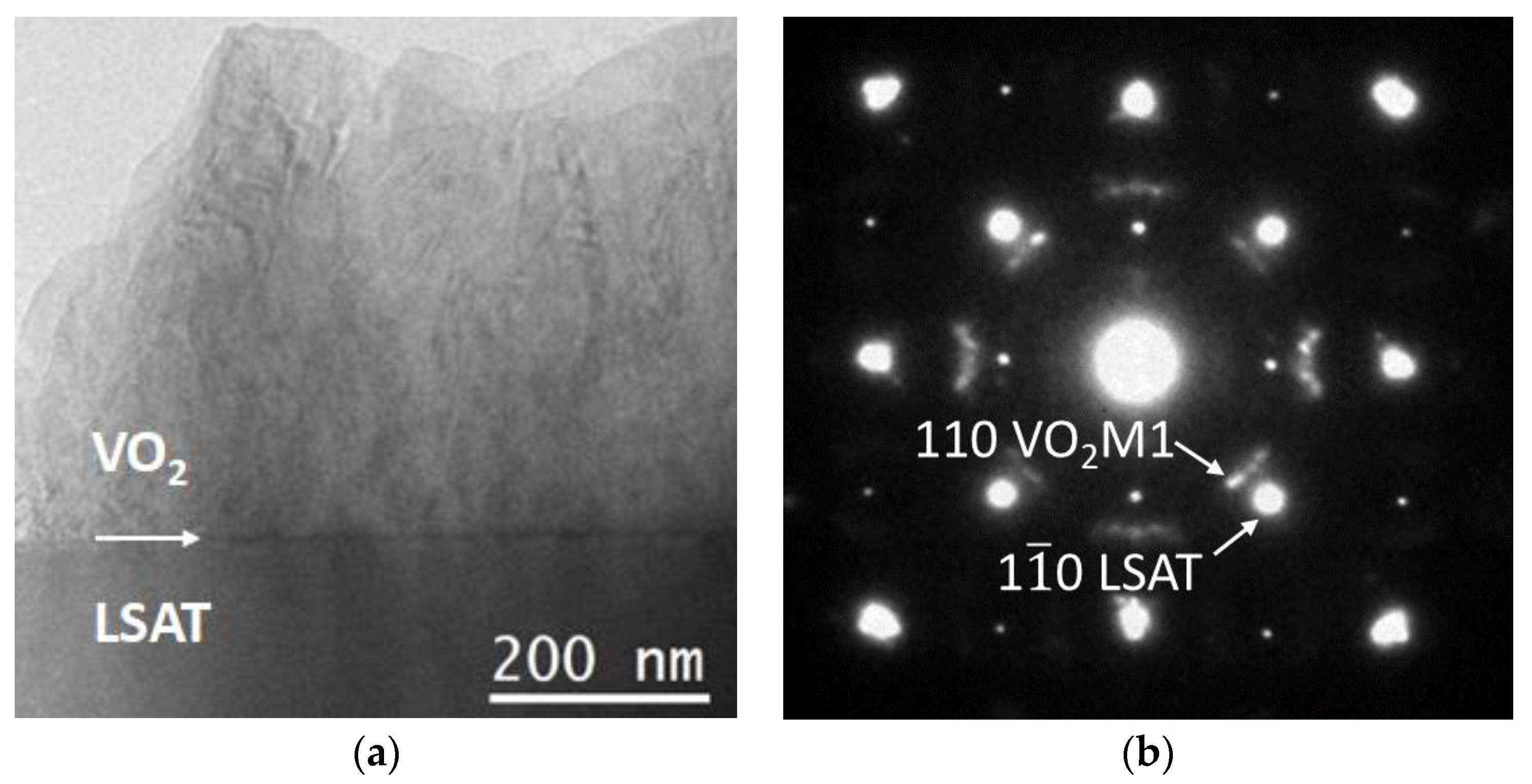
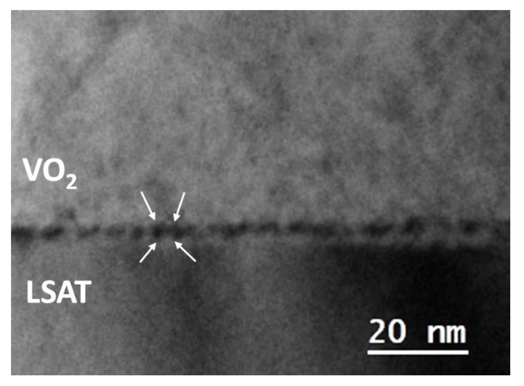
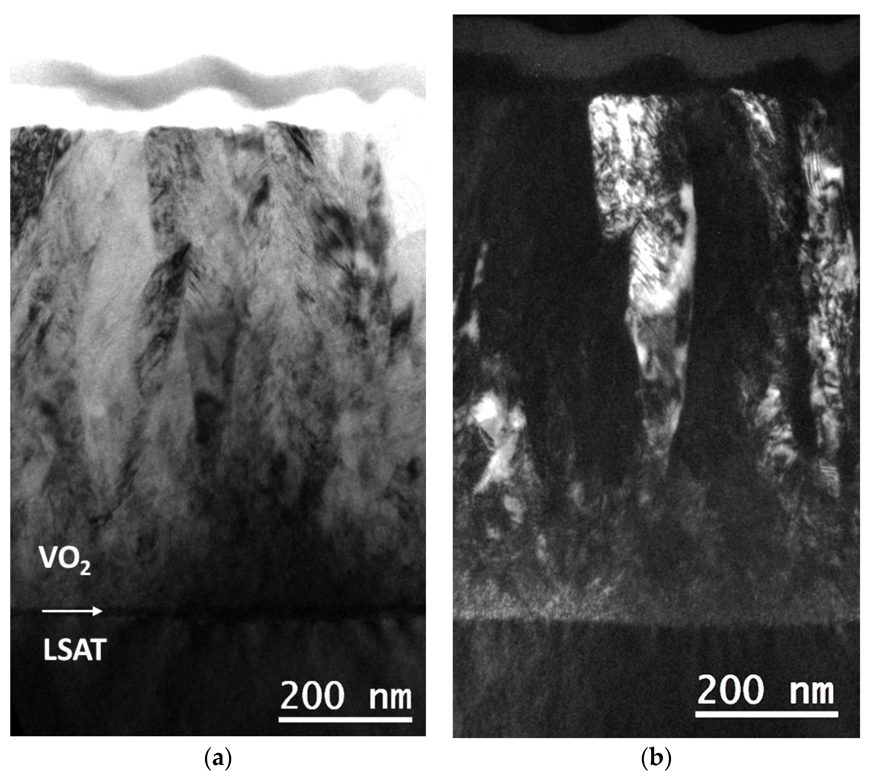
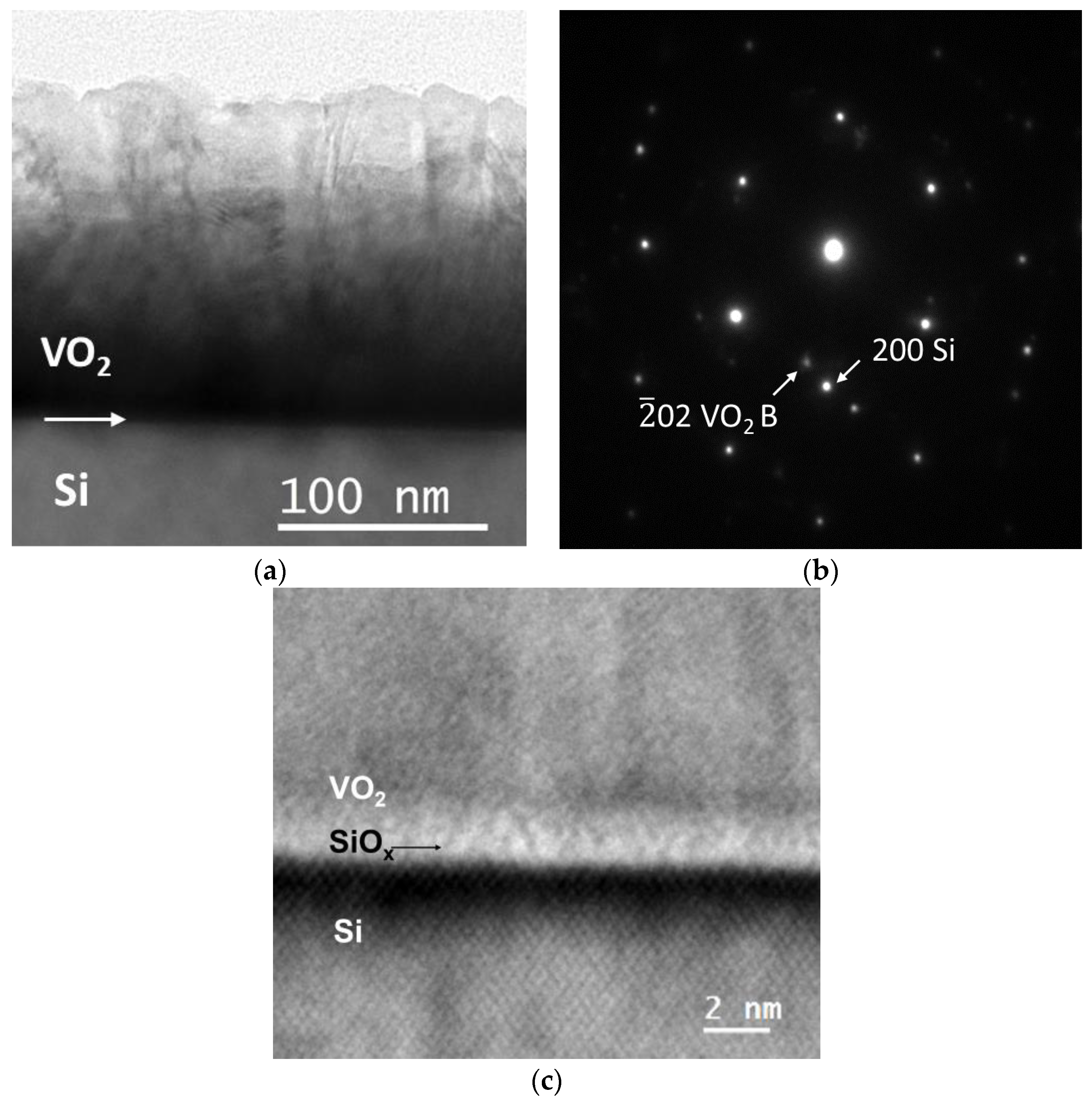
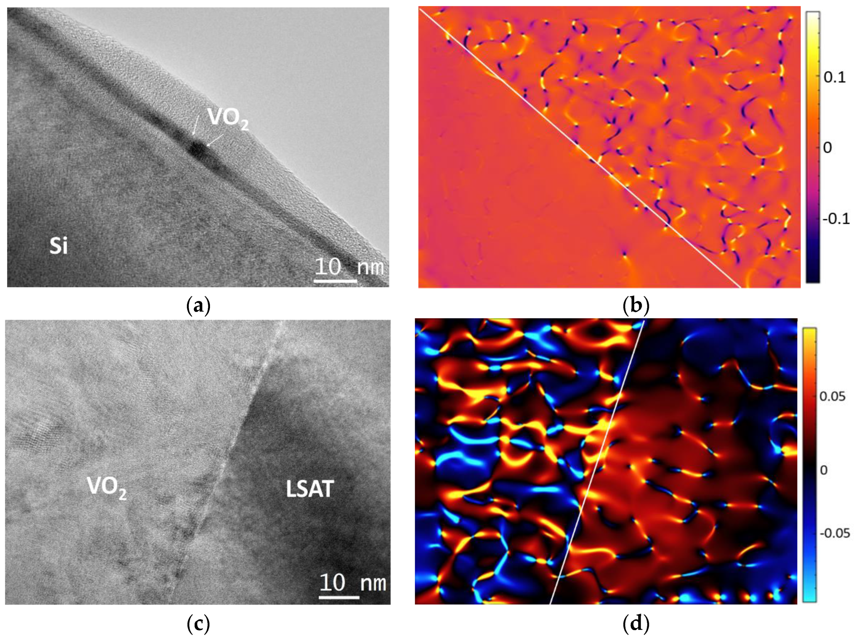
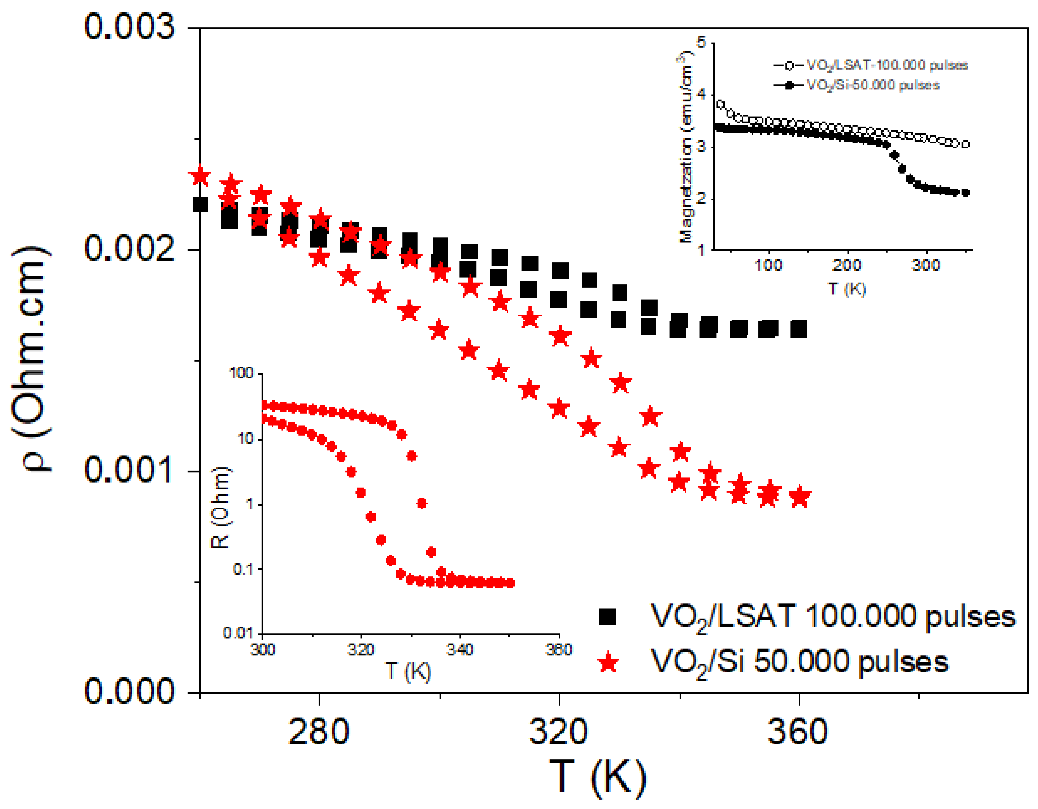
3. Result and Discussion

Qualitatively structural analysis by X-ray diffraction (XRD) in the samples revealed that several phases of VO2 are simultaneously present, due to the multiplicity of phases in the VO2 system. Their relative percentages, as well as the low thickness of the VO2 thin films, render it difficult to clearly distinguish the phases by XRD. Therefore, transmission electron microscopy (TEM) was subsequently employed for qualitative and quantitative structural phase identification.
A cross-sectional image of the S1 VO2 thin film grown on the LSAT substrate is shown in Figure 1a. The TEM investigations confirmed that the growth of the film by PLD was accomplished, and an overall coverage of VO2 on top of LSAT was achieved. The total thickness of this film was 720 nm, for 100,000 pulses. In terms of morphology, there was columnar growth of VO2, with a column width of around 170 nm, which is a common feature in the case of deposition of VO2 thin films on various substrates [32,33]. The selected area diffraction (SAD) pattern of S1 in Figure 1b was obtained by an area at the VO2/LSAT interface and shows reflections by both the substrate and film. The LSAT substrate is viewed along its [001] zone axis, whereas the VO2 film has a polycrystalline structure [29,34]. Furthermore, the SAD experiments revealed the co-existence of various VO2 polymorphs in the film, such as VO2 M1, VO2 B, VO2 A, and VO2 R. The structural parameters of these polymorphs are outlined in Table 1. In addition, the arcing of the VO2 spots and their alignment with the main ones of LSAT indicated that there is a tendency towards a structural relationship between the various VO2 phases in the thin film and the LSAT substrate. In more detail, this preferential orientation, with regards to the substrate can be summarized as
[ 110 ] LSAT / / [ 110 ] VO 2   M 1 ( 100 ) LSAT / / ( 002 ) VO 2   B   &   ( 010 ) LSAT / / ( 2 ¯ 02 ) VO 2   B
The interfacial quality of VO2/LSAT is depicted in more detail in the HRTEM images of Figure 2; a sharp and clear interface is illustrated, with minimum roughness. The VO2 M1 phase is dominant in the film area, both at the exact interface, as well as in the upper regions of the VO2 film, as demonstrated in Figure 2a. Moreover, the VO2 M1 and LSAT (110) planes, marked in the HRTEM image in Figure 2b, are perfectly aligned, in full agreement with the SAD pattern analysis.
The structural mismatch between VO2 and LSAT is expected to be accommodated for by the formation of misfit dislocation networks. The bright field (BF) image of Figure 3 illustrates a visualization of these misfit dislocations, as alternating dark and bright Moiré fringes, revealing the residual strain between the two lattices. The separation between the fringes, as measured both by BF images, as well as by satellite diffractions spots in common SAD patterns, was found to be dM = 1.94 nm on average, in accordance with the mismatch between VO2 M1 and LSAT.
The columnar morphology of the VO2 thin films has been better illustrated by diffraction contrast-imaging experiments. In Figure 4, two typical complementary BF and dark field (DF) images of the VO2/LSAT sample S1 are shown. The images were acquired using the g = 002 imaging vector of VO2. The columnar morphology of the VO2 area is apparent, with columns possessing typical widths of up to 170 nm towards the film’s free surface region and heights of up to the total film thickness, i.e., 720 nm in this case. Moreover, the VO2 columns have a high concentration of structural defects, which are mainly identified as twins, lying on {110} crystal planes. The SAD pattern of Figure 1b further confirms this observation.
The growth of VO2 thin film on Si substrates revealed similar structural features. Figure 5 shows typical results from the TEM observations of a VO2 film (S2) deposited with 20,000 pulses on Si (001). The VO2 film in Figure 5a also exhibits a columnar mode of growth, with average column widths of about 35 nm. The total film thickness is up to 167 nm. For thicker VO2 samples, i.e., S3 (50,000 pulses), where the total film thickness reaches 500 nm, the average column width proportionally increases to 93 nm in the film’s free surface region. Inside such columns, a significant number of planar defects, such as extended twins have been observed, too, in agreement with the results from VO2/LSAT. Figure 5b depicts a common SAD pattern of the film/substrate interfacial area. Si is oriented along its [011] zone axis, whereas reflections attributed to VO2 reveal a multiplicity of phases. Here, the 2 ¯ 02 spots of the VO2 B phase have been illustrated, for comparison. Diffraction analysis revealed that the VO2 films are polycrystalline, in full agreement with the films deposited on LSAT.
The HRTEM image in Figure 5c shows the VO2/Si interfacial area in greater detail, where a smooth interface has been revealed. There is an approximately 2 nm thick intrinsic amorphous layer of SiOx formed between the VO2 film and the Si substrate [35]. Therefore, although an epitaxial relationship between the film and substrate is not feasible in this case [27], there are some VO2 crystallites that aligned with or close to the main Si reflections, such as the VO2 B ones, whose [ 1 ¯ 01] direction is close to the Si [100] one.
The TEM analysis revealed the presence of several phases of VO2, irrespective of the thickness of the film and the type of substrate. Despite the variation in the number of pulses and film thickness, the structural quality was found, in general, to be quite good.
Most interplanar d spacings corresponded to the monoclinic VO2 (M1 type) but a good percentage of VO2 B and VO2 A phases were also found. Table 2 below summarizes the relative percentage of phases in the films, as estimated both by SAD pattern and HRTEM image analyses alike.
Post-experimental calculations of the residual strain present in the VO2 films have been accomplished by applying the geometric phase analysis (GPA) method on HRTEM images [36]. Figure 6 summarizes the main outcomes from these calculations. In the case of the Si substrate in Figure 6a,b, the strain is negligible, as it is predominately released due to the SiOx intrinsic amorphous layer formed between the substrate and film, along with the columnar VO2 morphology [37]. On the other hand, the growth of VO2 on top of LSAT as seen in Figure 6c,d is direct; however, the residual strain was still measured to be quite low and in the range of 5% on average, due to the columnar morphology of VO2 crystallites [37]. Only locally, the residual strain reaches values of up to 8–10%, mainly at areas with defects present, as shown in Figure 6d. According to the lattice parameters of LSAT (a = 0.387 nm) and VO2 M1 (Table 1) and their epitaxial relationship, the theoretical anticipated strain would be quite high, more than 17–20%; therefore, a great amount of strain relief is observed, due to the columnar morphology and polycrystalline nature of VO2. In addition, the average strain along the c axis (cVO2-cLSAT/cLSAT) would still be high, equal to 39%. However, the GPA strain maps suggest that the strain distribution does not change significantly throughout the film thickness.
∆A (resistance change), ∆T (sharpness), and ∆H (thermal hysteresis), and the reversibility of phase transition are all dependent on the quality of the film. Premkumar et al. reported a large variation in the resistance of films consisting of VO2 M1 and VO2 B phases at low temperature [38]. Considering the conduction behaviour, VO2 M1 and VO2 A are considered isolators (resistivities in the tens of Ohm.cm at room temperature, RT) and VO2 B a semiconductor (resistivities in the order of 10−2 Ohm.cm at RT), whereas VO2 R is considered to have a metallic character (resistivities in the order of 10−3 to 10−4 Ohm.cm at RT) [39]. However, a greater percentage of defects will lead to an increase in the resistivity of metallic VO2 due to the enhanced scattering of electrons [32], whereas in the case of semiconducting VO2, more energy levels are manifested in the band gap due to defects, leading to a resistivity decrease [40]. As a consequence, the resistivities of metallic and semiconducting films with various defects could become quite comparable at RT, and therefore the absolute values of the resistivities are not adequate to conclude an unambiguous attribution to the VO2 B or VO2 R phases. On the other hand, the MIT transition is usually assigned to a crystalline phase transformation from the higher temperature VO2 R phase to the lower temperature VO2 M1 phase at around 340 K, the transition being reversible and developing under a hysteretic character.
Temperature-dependent electron transport and magnetic measurements were performed under the assumption that any structural change would be reflected in both resistivity and magnetization behavior. The evolution of resistivity as a function of temperature for the thicker VO2 films deposited on LSAT and Si substrates (S1 and S3 samples, respectively) is shown in Figure 7. A decrease in the resistivity by more than 20% is observed for sample S1, and by more than 100% for sample S3 in the temperature range from 280 to 340 K, where the transition from the VO2 M1 to VO2 R polymorph is expected. Moreover, these transitions are reversible and of a hysteretic type with a maximum hysteretic width of about 20 K, as specific to the above-mentioned MIT. However, these variations are far lower than the optimal variations of resistance/resistivity by about three orders of magnitude, as observed in a similar film of VO2 deposited on a silica substrate at 600 °C, exemplified in the lower inset of Figure 7. There, resistance values in the order of 10 Ohm, corresponding to values of 10−3 Ohm.cm for resistivity are reported in both cases, below and above the MIT. In comparison, the resistance in the case of the VO2/silica at 600 °C is less than 10−1 Ohm above the MIT, resulting in a resistivity of about 10−5 Ohm.cm above 340 K, where a dominant R phase is expected. In this context, the much higher resistivity in the analyzed samples S1 and S3 at 340 K provides evidence for a dominant VO2 B phase at such temperatures. This result is in line with the TEM analysis, showing a significant amount of the VO2 B phase at RT, and gives support to the fact that only a low fraction of the initially present M1 phase was transformed into the R phase at the higher temperature, in both systems. That is, according to the resistivity data, the VO2 B phase is still highly dominant over the newly formed R phase at higher temperatures.
It is worth noticing from Table 2 that the initial content of the M1 phase was almost similar in both samples, whereas the resistivity of the S1 sample, already stabilizing 11% of the R phase, is higher than that of sample S3 at 340 K. This means that a higher fraction of the M1 phase has been transformed into the R phase in sample S3 as compared to S1. Tentatively, by the correlation of the resistivity results with the initial phase composition of the S1 and S3 films (see Table 2), it might be assumed that, for a more complete MIT, it is necessary to predominately avoid the formation of the VO2 R and secondary to avoid the formation of the rather stable VO2 B phases in the initial films (below the MIT).
The magnetic moments of the samples presented in the upper inset of the same figure are of the order of 10−5 emu (or a few emu/cm3 magnetization), which for such thin films, usually with oxygen vacancies, is specific to diluted magnetic oxide (DMO) behavior [41,42]. The different values and specific jumps in the magnetizations of the S1 and S3 films provide clear evidence for a different phase composition in the two films. For example, it is reported in [43] that the susceptibility is almost constant with the temperature in the isolator M1 phase (order of magnitude of 10−6 emu/g/Oe, bulk sample) but increases by one order of magnitude in the metallic R phase. In the current thin films, the susceptibilities are in the range of 10−3 emu/g/Oe, showing that, due to many defects in thin films (usually associated to oxygen vacancies), the DMO character is prevailing for the analyzed samples and at the same time hinders the much lower change in susceptibility along MIT. This is also the reason that no increase in the magnetization above RT is observed, in direct relation to the M1 to R phase transformation, as reported in [43]. The tiny structural changes of % order from the M1 to R type phase in the present are, however, still observable by only the most sensitive changes in the resistivity (3–4 orders of magnitude over about 100% M1 to R phase change). On the other hand, a decrease in the magnetization (by some 30%) is observed in sample S3 at about 260 K. The easier conversion of the B phase to the unstable M1 and further into the R phase has been reported in many cases and expectedly the more conductive (semiconducting) B phase should have a higher magnetization than the M1 phase, as well as an increased number of oxygen vacancies, also responsible for an increased magnetization in DMO systems; thus, we may tentatively assume that the decrease in magnetization over 260 K is due to the transformation of the B phase into the M1 phase.

4. Conclusions

VO2 thin films were sucessfully fabricated on LSAT and Si substrates using pulsed laser deposition with the aim of investigating the correlations between morpho-structural aspects, phase composition, and the related MIT transitions. Transmission electron microscopy techniques were used for a thorough structural investigation of the VO2 thin films, whereas resistivity and magnetic measurements were considered for the investigation of the specifically involved temperature-driven phase transitions. The films exhibited columnar growth regardless of the substrate. HRTEM imaging and SAD pattern acquisition revealed nanoscale grains of different phases, namely VO2 M1, VO2 A, VO2 B, and VO2 R. The thickest films exhibited the VO2 M1 phase as dominant (more than 50%) prior to the MIT transition but the VO2 B type was also stabilized in high amounts. The residual strain was relieved, predominantly due to the columnar morphology, along with the SiOx layer for the samples on Si substrates. In this context of very low residual strain, the less intense MITs in the thicker films were interpreted in terms of only a partial (a few %) M1 to R structural phase transition, specifically driven by the initial phase composition of the films. It was shown that the initial formation of the VO2 R phase, as well as the presence of the VO2 B phase, considerably diminishes both the sharpness and the resistance change in the VO2 films. According to this study, the lack of residual strain may impede the structural M1 to R transformation, in spite of a consistent presence of the M1-type phase in the films at RT.

Author Contributions

Conceptualization, A.D.; formal analysis, A.R. and A.D.; funding acquisition, A.D.; investigation, A.R., N.I., A.L., C.L., V.K., C.N.M. and A.D.; methodology, A.D.; project administration, A.D.; resources, A.D.; supervision, A.D.; visualization, A.D.; writing—original draft, A.R., N.I., A.L. and C.L.; writing—review and editing, V.K., C.N.M., and A.D. All authors have read and agreed to the published version of the manuscript.

Funding

This research was funded by EEA/Norway grants—Norway–Romania Collaborative Research Projects 2019, grant number RO-NO-2019-0498 (TEESM project). The NIMP authors also acknowledge the Romanian Ministry of Research, Innovation, and Digitalization in the framework of Core Program PN19-03 (Contract No. 21 N/08.02.2019). The APC was funded by the University of Stavanger and MDPI.

Data Availability Statement

All data is available throughout the manuscript.

Conflicts of Interest

The authors declare no conflict of interest.

References

  1. Zhou, Y.; Fan, F.; Liu, Y.; Zhao, S.; Xu, Q.; Wang, S.; Luo, D.; Long, Y. Unconventional smart windows: Materials, structures and designs. Nano Energy 2021, 90, 106613. [Google Scholar] [CrossRef]
  2. Lombard, L.P.; Ortiz, J.; Pout, C. A review on buildings energy consumption information. Energy Build. 2008, 40, 394–398. [Google Scholar] [CrossRef]
  3. Wang, M.; Xing, X.; Perepichka, I.F.; Shi, Y.; Zhou, D.; Wu, P.; Meng, H. Electrochromic smart windows can achieve an absolute private state through thermochromically engineered electrolyte. Adv. Energy Mater. 2019, 9, 1900433. [Google Scholar] [CrossRef]
  4. Searchinger, T.D.; Beringer, T.; Holtsmark, B.; Kammen, D.M.; Lambin, E.F.; Lucht, W.; Raven, P.; Ypersele, J.P.V. Europe’s renewable energy directive poised to harm global forests. Nat. Commun. 2018, 9, 3741. [Google Scholar] [CrossRef] [PubMed] [Green Version]
  5. Shin, M.; Baltazar, J.C.; Haberl, J.S.; Frazier, E.; Lynn, B. Evaluation of the energy performance of a net zero energy building in a hot and humid climate. Energy Build. 2019, 204, 109531. [Google Scholar] [CrossRef]
  6. Zhang, G.; Li, X.; Shi, W.; Wang, B.; Cao, Y. Influence of occupant behaviour on the energy performance of variable refrigerant flow systems for office buildings: A case study. J. Build. Eng. 2019, 22, 327–334. [Google Scholar] [CrossRef]
  7. Granqvist, C.G. Recent progress in thermochromics and electrochromics: A brief survey. Thin Solid Films 2016, 614, 90–96. [Google Scholar] [CrossRef]
  8. Llordes, A.; Garcia, G.; Gazquez, J.; Milliron, D.J. Tunable near-infrared and visible light transmittance in nanocrystal-in-glass composites. Nature 2013, 500, 323–326. [Google Scholar] [CrossRef] [Green Version]
  9. Cai, G.; Wang, J.; Lee, P.S. Next-generation multifunctional electrochromic devices. Acc. Chem. Res. 2016, 49, 1469–1476. [Google Scholar] [CrossRef]
  10. Ke, Y.; Zhou, C.; Zhou, Y.; Wang, S.; Chan, S.H.; Long, Y. Emerging thermal responsive materials and integrated techniques targeting the energy-efficient smart window application. Adv. Funct. Mater. 2018, 28, 1800113. [Google Scholar] [CrossRef]
  11. Khandelwal, H.; Schenning, A.P.H.J.; Debije, M.G. Infrared regulating smart window based on organic materials. Adv. Energy Mater. 2017, 7, 1602209. [Google Scholar] [CrossRef] [Green Version]
  12. Amasawa, E.; Sasagawa, N.; Kimura, M.; Taya, M. Design of a new energy harvesting electrochromic window based on an organic polymeric dye, a cobalt couple, and PProDOT-Me2. Adv. Energy Mater. 2014, 4, 1400379. [Google Scholar] [CrossRef]
  13. Mann, D.; Yeung, C.; Habets, R.; Vroon, Z.; Buskens, P. Comparative building energy simulation study of static and thermochromically adaptive energy-efficient glazing in various climate regions. Energies 2020, 13, 2842. [Google Scholar] [CrossRef]
  14. Gagaoudakis, E.; Michail, G.; Aperathitis, E.; Kortidis, I.; Binas, V.; Panagopoulou, M.; Raptis, Y.S.; Tsoukalas, D.; Kiriakidis, G. Low temperature rf-sputtered thermochromic VO2 films on flexible glass substrates. Adv. Mater. Lett. 2017, 8, 757–761. [Google Scholar] [CrossRef]
  15. Granqvist, C.G. Electrochomics and thermochomics: Towards a new paradigm for energy efficient buildings. Mater. Today Proc. 2016, 3, S2–S11. [Google Scholar] [CrossRef]
  16. Vernardou, D.; Pemble, M.E.; Sheel, D.W. In-situ FTIR studies of the growth of vanadium dioxide coatings on glass by atmospheric pressure chemical vapour deposition for VCl4 and H2O system. Thin Solid Film. 2007, 515, 8768–8770. [Google Scholar] [CrossRef]
  17. Koo, H.; You, H.W.; Ko, K.E.; Kwon, O.J.; Chang, S.H.; Parka, C. Thermochromic properties of VO2 thin film on SiNx buffered glass substrate. Appl. Surf. Sci. 2013, 277, 237–241. [Google Scholar] [CrossRef]
  18. Pouget, J.P.; Launois, H.; D’Haenens, J.P.; Merenda, P.; Rice, T.M. Electron Localization Induced by Uniaxial Stress in Pure VO2. Phys. Rev. Lett. 1975, 13, 35. [Google Scholar] [CrossRef]
  19. Narayan, J.; Bhosle, V.M. Phase transition and critical issues in structure-property correlations of vanadium oxide. J. Appl. Phys. 2006, 100, 103524. [Google Scholar] [CrossRef]
  20. Bayati, M.R.; Molaei, R.; Wub, F.; Budai, J.D.; Liu, Y.; Narayan, R.J.; Narayan, J. Correlation between structure and semiconductor-to-metal transition characteristics of VO2/TiO2/sapphire thin film heterostructures. Acta Mater. 2013, 61, 7805–7815. [Google Scholar] [CrossRef]
  21. Burkhardt, W.; Christmann, T.; Franke, S.; Kriegseis, W.; Meister, D.; Meyer, B.K. Tungsten and fluorine co-doping of VO2 films. Thin Solid Films 2002, 402, 226. [Google Scholar] [CrossRef]
  22. Ruzmetov, D.; Ramanathan, S. Thin Film Metal Oxides: Fundamentals and Applications in Electronics and Energy; Springer: New York, NY, USA, 2010. [Google Scholar]
  23. Choi, Y.; Jung, Y.; Kim, H. Low-temperature deposition of thermochromic VO2 thin films on glass substrates. Thin Solid Films. 2016, 615, 437–445. [Google Scholar] [CrossRef]
  24. Kolenatý, D.; Vlček, J.; Bárta, T.; Rezek, J.; Houška, J.; Haviar, S. High-performance thermochromic VO2-based coatings with a low transition temperature deposited on glass by a scalable technique. Sci. Rep. 2020, 10, 11107. [Google Scholar] [CrossRef]
  25. Malarde, D.; Powell, M.J.; Quesada-Cabrera, R.; Wilson, R.L.; Carmalt, C.J.; Sankar, G.; Parkin, I.P.; Palgrave, R.G. Optimized Atmospheric-Pressure Chemical Vapor Deposition Thermochromic VO2 Thin Films for Intelligent Window Applications. ACS Omega 2017, 2, 1040−1046. [Google Scholar] [CrossRef] [Green Version]
  26. Li, D.; Li, M.; Pan, J.; Luo, Y.; Wu, H.; Zhang, Y.; Li, G. Hydrothermal Synthesis of Mo-Doped VO2/TiO2 Composite Nanocrystals with Enhanced Thermochromic Performance. Appl. Mater. Interfaces 2014, 6, 6555−6561. [Google Scholar] [CrossRef]
  27. Manning, T.D.; Parkin, I.P. Vanadium(IV) oxide thin films on glass and silicon from the atmospheric pressure chemical vapour deposition reaction of VOCl3 and water. Polyhedron 2004, 23, 3087–3095. [Google Scholar] [CrossRef]
  28. Chang, T.; Cao, X.; Li, N.; Long, S.; Gao, X.; Dedon, L.R.; Sun, G.; Luo, H.; Jin, P. Facile and Low-Temperature Fabrication of Thermochromic Cr2O3/VO2 Smart Coatings: Enhanced Solar Modulation Ability, High Luminous Transmittance and UV-Shielding Function. Appl. Mater. Interfaces 2017, 9, 26029−26037. [Google Scholar] [CrossRef]
  29. Kim, D.H.; Kwok, H.S. Pulsed laser deposition of VO2 thin films. Appl. Phys. Lett. 1994, 65, 3188. [Google Scholar] [CrossRef]
  30. Chang, T.; Zhu, Y.; Huang, J.; Luo, H.; Jin, P.; Cao, X. Flexible VO2 thermochromic films with narrow hysteresis loops. Sol. Energy Mater. Sol. Cells 2021, 219, 110799. [Google Scholar] [CrossRef]
  31. Kim, C.Y.; Kim, S.H.; Kim, S.J.; An, K.S. VO2 (110) film formation on TiO2(110) through post-reduction of ALD grown vanadium oxide. Appl. Surf. Sci. 2014, 313, 368–371. [Google Scholar] [CrossRef]
  32. Jian, J.; Chen, A.; Zhang, W.; Wang, H. Sharp semiconductor-to-metal transition of VO2 thin films on glass substrates. J. Appl. Phys. 2013, 114, 244301. [Google Scholar] [CrossRef]
  33. Jian, J.; Chen, A.; Chen, Y.; Zhang, X.; Wang, H. Roles of strain and domain boundaries on the phase transition stability of VO2 thin films. Appl. Phys. Lett. 2017, 111, 153102. [Google Scholar] [CrossRef]
  34. Yamagushi, I.; Manabe, T.; Tsyuchia, T.; Nakajima, T.; Sohma, M.; Kumagai, T. Preparation and Characterization of Epitaxial VO2 Films on Sapphire Using Postepitaxial Topotaxy Route via Epitaxial V2O3 Films. Jpn. J. Appl. Phys. 2008, 47, 1022. [Google Scholar] [CrossRef]
  35. Goodnick, S.M.; Fathipour, M.; Ellsworth, D.L.; Wilmsen, C.W. Effects of a thin SiO2 layer on the formation of metal–silicon contacts. J. Vac. Sci. Technol. 1981, 18, 949. [Google Scholar] [CrossRef]
  36. Hÿtch, M.J.; Snoek, E.; Kilaas, R. Quantitative measurement of displacement and strain fields from HREM micrographs. Ultramicroscopy 1998, 74, 131. [Google Scholar] [CrossRef]
  37. Kehagias, T.; Delimitis, A.; Kominou, P.; Iliopoulos, E.; Dimakis, E.; Georgakilas, A.; Nouet, G. Misfit accommodation of compact and columnar InN epilayers grown on Ga-face GaN (0001) by molecular-beam epitaxy. Appl. Phys. Lett. 2005, 86, 151905. [Google Scholar] [CrossRef]
  38. Premkumar, P.A.; Toeller, M.; Radu, J.P.; Adelmann, C.; Schaekers, M.; Meersschaut, J.; Conard, T.; Elshochta, S.V. Process Study and Characterization of VO2 Thin Films Synthesized by ALD Using TEMAV and O3 Precursors. ECS J. Solid State Sci. Technol. 2012, 1, P169–P174. [Google Scholar] [CrossRef]
  39. Lee, S.; Ivanov, I.N.; Keum, J.K.; Lee, H.N. Epitaxial stabilization and phase instability of VO2 polymorphs. Sci. Rep. 2016, 6, 19621. [Google Scholar] [CrossRef] [PubMed] [Green Version]
  40. Brassard, D.; Fourmaux, S.; Jean-Jacques, M.; Kieffer, J.C.; El Khakani, M.A. Grain size effect on the semiconductor-metal phase transition characteristics of magnetron-sputtered VO2 thin films. Appl. Phys. Lett. 2005, 87, 051910. [Google Scholar] [CrossRef]
  41. Tolea, F.; Sorescu, M.; Diamandescu, L.; Iacob, N.; Tolea, M.; Kuncser, V. Unidirectional Magnetic Anisotropy in Molybdenum Dioxide–Hematite Mixed-Oxide Nanostructures. Nanomaterials 2022, 12, 938. [Google Scholar] [CrossRef] [PubMed]
  42. Tolea, F.; Grecu, M.N.; Kuncser, V.; Constantinescu, S.G.; Ghica, D. On the role of Fe ions on magnetic properties of doped TiO2 nanoparticles. Appl. Phys. Lett. 2015, 106, 142404. [Google Scholar] [CrossRef]
  43. Zhang, R.; Fu, Q.S.; Yin, C.Y.; Li, C.L.; Chen, X.H.; Qian, G.Y.; Lu, C.L.; Yuan, S.L.; Zhao, X.J.; Tao, H.Z. Understanding of metal-insulator transition in VO2 based on experimental and theoretical investigations of magnetic features. Sci. Rep. 2018, 8, 17093. [Google Scholar] [CrossRef] [PubMed]
Figure 1. (a) TEM image of S1 VO2 thin film on LSAT substrate, showing the general morphology; (b) SAD pattern from the interface area between VO2 and the substrate.
Inorganics 10 00220 g001
Figure 2. HRTEM images from the VO2/LSAT interface showing the interfacial quality and the dominant VO2 M1 phase.
Inorganics 10 00220 g002
Figure 3. Cross-sectional image of the VO2/LSAT interfacial area, viewed by the [001] LSAT zone axis.
Inorganics 10 00220 g003
Figure 4. (a) BF image taken from S1 revealing the columnar growth of VO2 thin film grown on LSAT; (b) complementary DF image from the same area, obtained with g = 002.
Inorganics 10 00220 g004
Figure 5. Microscopy results of the S2 VO2 thin film on Si substrate: (a) conventional TEM image exhibiting columnar growth; (b) common SAD pattern taken from the interface area with Si being in the [011] zone axis; (c) HRTEM image of the VO2/Si interfacial area showing its structural quality and the SiOx intrinsic layer.
Inorganics 10 00220 g005
Figure 6. Typical GPA results from the VO2 thin films: (a,c) HRTEM images; (b,d) corresponding GPA strain maps of VO2/Si and VO2/LSAT, respectively.
Inorganics 10 00220 g006
Figure 7. Temperature-dependent resistivity of S1 and S3 VO2 films on LSAT and Si substrate, respectively. The upper inset shows the temperature-dependent magnetizations of the same films under a 300 Oe applied magnetic field, whereas the lower inset illustrates the temperature-dependent resistance of a similar VO2 film, deposited on silica at 600 °C.
Inorganics 10 00220 g007
Table 1. Structural parameters of the various VO2 polymorphs found in the thin films.
VO2 PhaseStructureLattice Parameters
M1Monoclinica = 0.575 nm
b = 0.454 nm
c = 0.538 nm
β = 122.6°
ATetragonala = 0.844 nm
c = 0.767 nm
BMonoclinica = 0.121 nm
b = 0.37 nm
c = 0.643 nm
β = 106.9°
RTetragonala = 0.456 nm
c = 0.286 nm
Table 2. Percentage of the dominant VO2 phases detected in the thin films grown on LSAT and Si substrates.
SamplesVO2 M1VO2 RVO2 AVO2 B
S15411629
S240-1545
S353-1235
Publisher’s Note: MDPI stays neutral with regard to jurisdictional claims in published maps and institutional affiliations.

