1. Introduction
Microwave photonics (MWP), which uses optical components to generate, transport and process high-frequency microwave signals, has drawn significant interest in this research field [
1]. The traditional MWP, also known as ‘bulk’ MWP, is mainly based on discrete optical components, and the lack of scalability seriously limits its applications. To address this issue, tremendous efforts have been made on integrated microwave photonics (IMWP) [
2]. By miniaturizing MWP systems into a single chip, IMWP provides a new way to achieve large-scale microwave systems, such as programmable microwave processors [
3], all-optical analog-to-digital converters [
4] and photonics-based radars [
5].
In IMWP, the radio-frequency signal is converted into the optical domain using electro-optical modulators. The linearity of the modulator is a key performance factor in IMWP. Non-linear distortions caused by the modulation will seriously limit the spurious-free dynamic range (SFDR) of microwave signals. Thus, achieving high-speed, low-driven voltage and linearity modulators is one of the primary goals. However, in conventional photonics platforms, including silicon-on-insulator (SOI) [
6], silicon nitride (SiN
) [
7], bulk lithium niobate (LN) [
8] and III-V materials [
9], building a high-performance modulator with the capability mentioned above is facing critical challenges.
In particular, the free carrier dispersion in the SOI platform is a nonlinear electro-optical effect; SiN does not support active devices due to its insulating nature; III-V materials do not allow low-loss waveguides; bulk LN is an attractive material for microwave photonics owing to its ultra-wide transparency window and large second-order electro-optic coefficient; however, bulk LN devices have a large footprint and low integration density.
Recently, thin-film lithium niobate (TFLN) has emerged as a revolutionary IMWP platform [
10,
11]. TFLN possesses not only the excellent material properties of LN but also the thin-film advantages of strong optical confinement. Within the past few years, benefiting from the rapid development of manufacturing methods for TFLN microstructures, low-voltage and ultra-high bandwidth Mach–Zehnder modulators (MZMs) have been demonstrated [
12,
13,
14,
15,
16].
In the TFLN platform, the linearity of modulators is mostly limited by the sinusoidal transfer function of the MZM. Additionally, the TFLN platform enables advanced modulation schemes, such as ring-assisted MZMs [
17], dual-parallel MZMs [
18,
19] and cascade MZMs [
20], which could further improve the linearity performances of TFLN modulators. To the best of our knowledge, the highest SFDR achieved in the TFLN platform is 99.6 dB·Hz
[
14], and the advanced modulation schemes are yet to be explored.
In this work, we investigate a linearity-enhanced modulation scheme on the thin-film lithium niobate platform: the dual-parallel Mach–Zehnder modulator (DP-MZM). By setting the optical and electrical splitting ratios at a specific condition, the third-order intermodulation distortions (IMD3) of the child MZMs cancel with each other whereas the first-order harmonics (FH) reaches the maximum. To simplify the operation scheme, we use passive optical devices to control the power and phase of the child MZMs.
Specifically, the arbitrary ratio optical power splitter is achieved based on cascaded multimode interferometers connected with passive phase shifters. The fabricated DP-MZMs achieve a spurious-free dynamic range of 110.7 dB·Hz at 1 GHz, which is about a 5.5 dB enhancement compared to conventional MZMs. The E-O response decayed about 1.9 dB from 10 MHz to 40 GHz, and the extrapolated E-O 3 dB bandwidth is expected to be 70 GHz. A half-wave voltage of 2.8 V was also achieved.
2. Methods
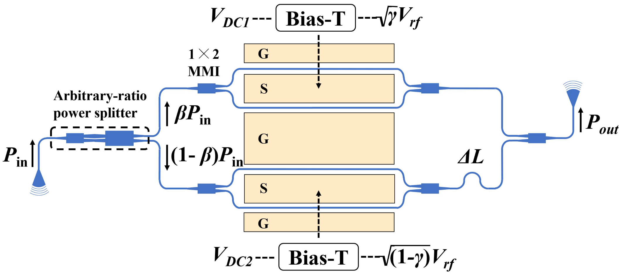
The schematic view of the proposed DP-MZM is shown in
Figure 1. Two grating couplers designed for the transverse electric (TE) polarization at 1550 nm are used for off-chip coupling. An arbitrary ratio power splitter is achieved based on two cascaded multimode interferometers connected with passive phase shifters. The normalized output power of the arbitrary ratio power splitter can be expressed as
and
. Two identical MZMs with 1-cm long phase shifters are connected in parallel.
The sub-MZMs are biased at opposite quadrature transmission points () with different DC bias voltages denoted as and , respectively. Under these specific bias conditions, the third-order intermodulation distortion components of the sub-MZMs are out of phase. Thus, with different RF levels of and , the IMD3 components could completely cancel out with each other.
The Mach–Zehnder interferometer (MZI) of the parent MZM is designed to be asymmetrical with a path difference
= 125
m, and thus effective orthogonality of the outputs from the child MZMs can be realized at a proper wavelength [
21]. To balance the modulation efficiency and the optical loss, the electrode gap is fixed as 6
m, and the simulated metal absorption loss is lower than 0.01 dB/cm. The thickness of the electrodes is 1
m, and the width of the signal and ground electrodes are 20 and 100
m, respectively.
The analytic model of silicon DP-MZM was proposed in [
18]. Since LN has a linear electro-optical (E-O) effect, the phase difference
induced by modulation can be written as:
, where
is the scaling factor. In the two-tone test, the amplitude of two signals
and
should be equal:
. Then, under the bias conditions mentioned above, the amplitude of the FH and IMD3 components of the DP-MZM can be expressed as [
18]:
One can see that, to eliminate the IMD3 components,
and
should satisfy the following condition:
Under the above condition, the IMD3 components can be completely eliminated. However, the amplitude of the FH components is also influenced by
and
. Hence, one should set the optical and electrical splitting ratios at a specific condition that the third-order intermodulation distortions (IMD3) of the child MZMs cancel with each other, while the first-order harmonics (FH) reaches the maximum. Using Equations (
1) and (
3), the specific condition is obtained:
= 0.11,
= 0.8.
In the DP-MZM operation scheme, the specific optical and electrical splitting ratios ( = 0.11, = 0.8) are needed so that the IMD3 component of the child MZMs cancel with each other while the first-order harmonics reaches the maximum. For a single 1 × 2 or 2 × 2 multimode interferometer (MMI), only five discrete values of splitting ratio can be achieved, namely 15/85, 28/72, 50/50, 72/28 and 85/15. Since the optical splitting ratio cannot be simply obtained by the multimode interferometer or Y-branch, the previous studies used thermal optical switches and additional power supplies to achieve the desired , which makes the device complex and power inefficient.
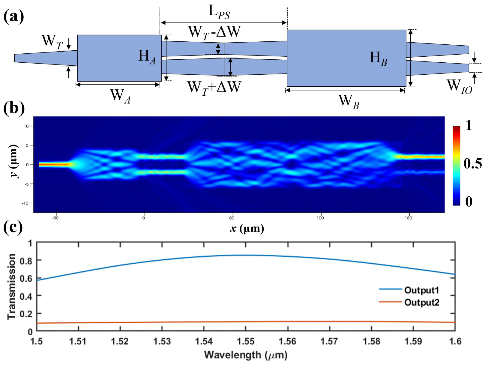
In this work, we used passive and fabrication-tolerant arbitrary ratio optical splitters instead of thermal optical switches, which simplify the operation scheme and improve the device stability. The schematic view of the arbitrary ratio optical splitter is shown in
Figure 2a. A 50/50 1 × 2 MMI and a 50/50 2 × 2 MMI are connected by a passive phase shifter (PS). The PS is formed by waveguide tapers with the same width variation
W but in opposite directions: the upper taper is narrowed, while the lower taper is enlarged.
The W will not change with fabrication deviations, and the MMI is also a fabrication-friendly structure. Hence, the proposed optical splitter has relaxed width-error sensitivity. The length of PS L, together with the W, determines the phase difference between the upper and lower input port of the 2 × 2 MMI. To achieve , the design parameters of the arbitrary ratio optical splitter are as follows: W = 200 nm, W = 1.5 m, W = 1 m, W = 44 m, W = 128.5 m, H = 8 m, H = 12 m, L = 21.5 m.
The simulated mode profile for a device with the design parameters given above is shown in
Figure 2b, calculated using full finite-difference time-domain method (FDTD, Ansys Lumerical). The simulated insertion loss (IL) is 0.2 dB at 1550 nm. Due to the limited bandwidth of the MMI, IL increases with wavelengths deviating from 1550 nm (IL = 1.3 dB,
= 1600 nm). However, the normalized coupling ratio
has a weaker dispersion, and it varies from 0.11 to 0.134 over a large bandwidth of 100 nm. Hence, with the proposed structure, accurate and wavelength-insensitive
can be obtained without any active control.
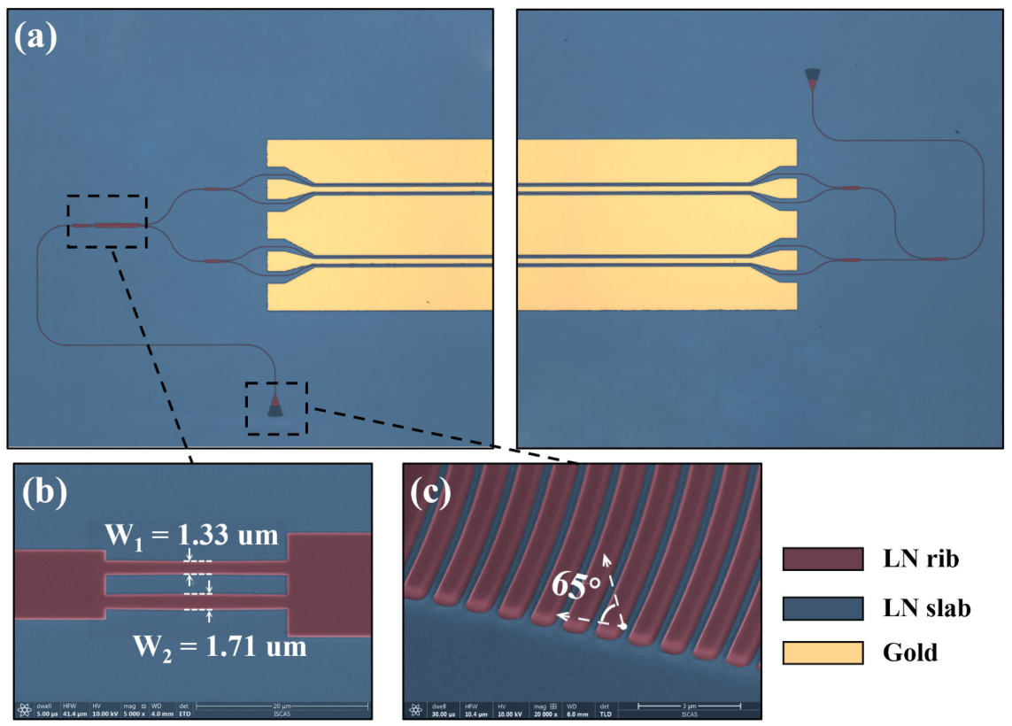
The devices (
Figure 3a) were fabricated on a x-cut lithium niobate-on-insulator with 400-nm thick TFLN and a 3-
m buried oxide layer. First, a piranha solution (H
SO
/H
O
= 3:1, 80
C) followed by an oxygen plasma were used to ensure a clean wafer surface. Next, a microlithography adhesion promoter named Surpass 3000 was spin-coated on the wafer first to improve the adhesion of e-beam hydrogen silsesquioxane (HSQ). Then, we coated the wafer with HSQ at 3000 rpm for 60 s and pre-baked for 4 min at 80
C. The e-beam lithography was performed by the JBX-8100FS system with an accelerating voltage of 100 KV.
E-beam lithography process has the advantages of excellent line width control and great design flexibilities. As is shown in
Figure 3b, the measured value of
and
were 1.33
m and 1.71
m, respectively. The slight dimensional deviation (<30 nm) ensures a good agreement between the designed and demonstrated value of
. After developing the resist, the TFLN was partially dry-etched by 200 nm using argon-based inductively coupled plasma reactive ion etching. The etch selectivity between the LN and HSQ was approximately 1:2.5.
The remaining resist was then removed by a buffered oxide etch solution, and the by-product formed in etching was removed by a RCA solution (NH
OH:H
O
:H
O = 1:1:5) at 60
C for 30 min. From the SEM image of the grating couplers taken after wet-etching (
Figure 3c), one can see that the optimized etch process resulted in a smooth sidewall and an approximately 65
sidewall angle.
In the argon-based dry-etch method, the non-vertical sidewall is inevitable due to the redeposition of LN. Hence, in the early stage of our experiment, we measured the waveguide sidewall angle using focused ion beam (FIB). To obtain precise and accurate simulation results, this factor is considered throughout the simulation process.
At the final step, 1-m thick gold electrodes were fabricated using UV lithography and a standard lift-off process. The fabrication processes, such as dry-etching, cleaning and deposition, are all commonly used in photonics integrated circuits (PIC) fabrications. The minimum line width of this device is around 450 nm, which can be easily achieved using EBL systems or i-line UV photography.
3. Results
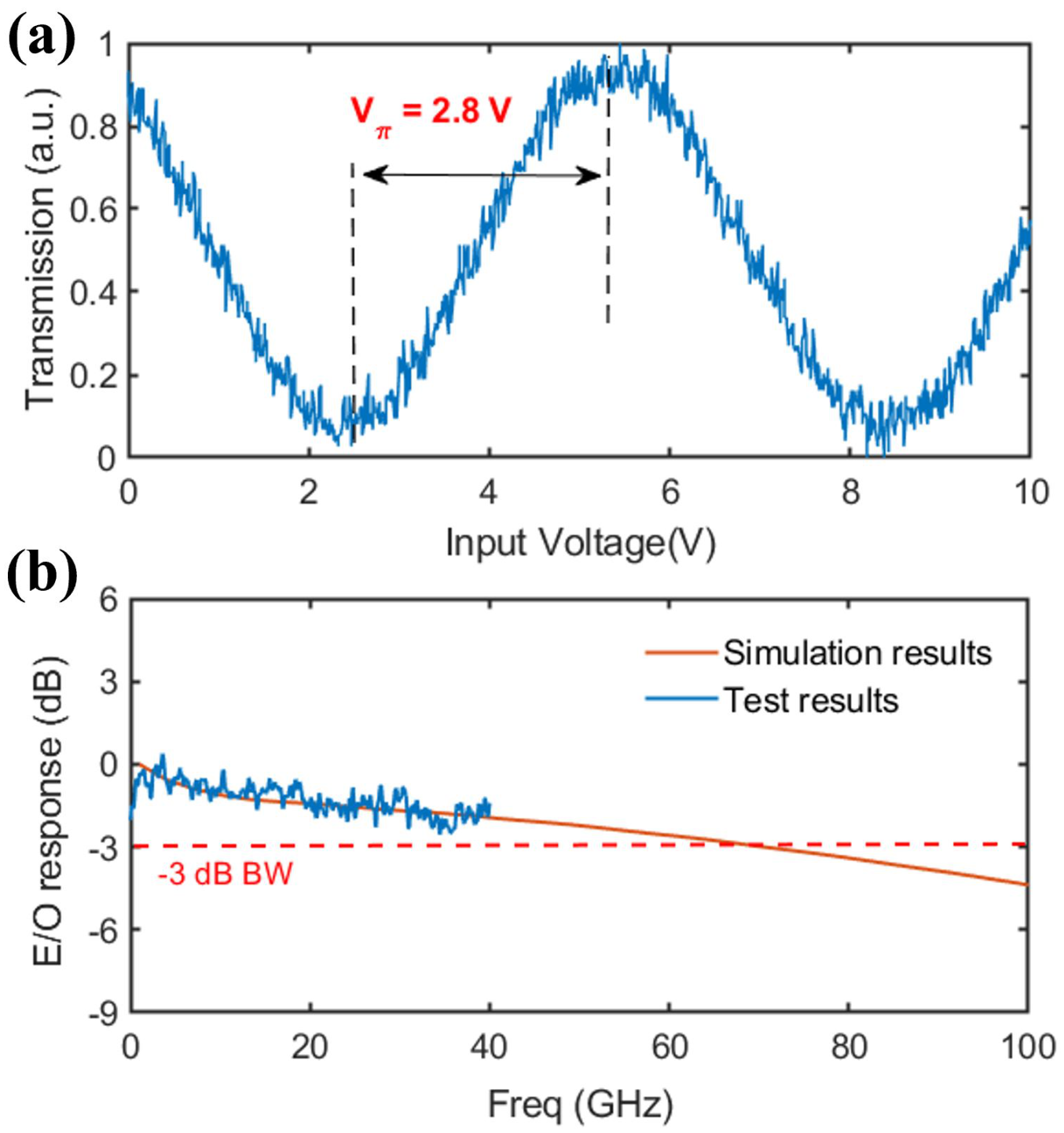
The DC characterization was performed first. A tunable laser fixed at 1550 nm was used as the optical source. The measured coupling loss of the grating coupler was 5.1 dB/facet. We extracted the waveguide propagation loss using the cut-back method. For a waveguide width of 1 m, the propagation loss was measured to be 0.7 dB/cm. The total on-chip insertion loss of the DP-MZM was 2.1 dB, consisting of 0.9 dB waveguide propagation loss, 1.2 dB insertion loss of the MMIs. Then, the half-wave voltage (V) was measured for one of the child MZMs.
The measured transmission spectrum under a 100-kHz triangular wave voltage sweep with 10 V peak-to-peak amplitude is shown in
Figure 4a. The V
is measured to be 2.8 V for a 1-cm long MZM, corresponding to a modulation efficiency of 2.8 V·cm. It is worth mentioning that the demonstrated MZMs had a wider electrode gap of 7
m due to fabrication errors, which led to the lower modulation efficiency compared to the simulation.
The experimental splitting ratio was then measured using a test structure in which the input and output ports of the splitter were directly connected to the grating coupler. The fabricated splitter achieved the desired = 0.11 ± 0.1 from 1537 to 1562 nm. Compared to the simulated results, the fabricated device showed a larger dispersion; however, the desired was achieved among the C-band.
Then, characterizations of the small-signal were performed. The output optical signal was received by a high-bandwidth electro-optical (E-O) bandwidth photodetector, which was then connected to the vector network analyzer (VNA). A pair of 67 GHz GSG high-frequency RF probes were used for launch and termination. By de-embedding the known E-O S21 parameters of the PD, the E-O response of the proposed DP-MZM was then obtained.
As is shown in
Figure 4b, the E-O response decayed about 1.9 dB from 10 MHz to 40 GHz. To justify the measured E-O response, the average modulation voltage model was used to simulate the E-O response [
22]. The E-O response of the MZM is given as:
where r(
) is the modulation response,
and
are the input and output reflection coefficient,
is the characteristic impedance,
and
are the source impedance and terminating impedance.
and
are the single pass average voltage experienced by a photon due to co-propagation and counter-propagation between microwave and optical wave, where
and
,
l is the phase shifter length,
is the propagation constant of microwave, and
is the complex phase of the optical wave.
It is worth mentioning that the values of
,
,
used in this simulation were all extracted from experiments. As shown in
Figure 4b, the simulated E-O responses agreed well with the test results, and the E-O 3-dB bandwidth is expected to be 70 GHz.
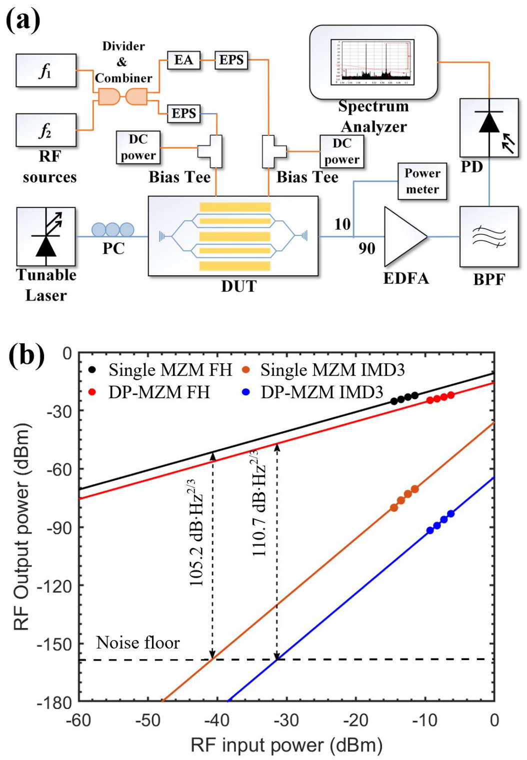
Next, the two-tone test was performed with the measurement step shown in
Figure 5a. A tunable laser together with a polarization controller (PC) was used as the optical source. The two-tone signal was formed using two separate RF sources and an electrical combiner. The interval between
and
was 10 MHz, and the center frequency was 1 GHz. A 50/50 electrical power divider was used to divide the signal into two. One path was connected to an electrical attenuator (EA) to obtain the desired electrical splitting ratio
.
To ensure both two-tone signals are fed into the child MZMs with the same phase, a tunable electrical phase shifter (EPS) was added into each path of the two-tone signals. Two DC sources were used to control the operation point of the MZMs. An erbium-doped fiber amplifier (EDFA) was used to amplify the optical output power during the test. Then, the optical signal reached the square-law photodetector (PD) with a bandwidth of 50-GHz and a responsivity of 0.7 A/W. In the two-tone test, the measured IMD3 SFDR is affected by many factors, such as the input optical power on the photodetector, the responsivity of PD, the electrical link insertion loss, the nonlinearity of input signal, the noise floor of the measurement system and the MZM itself.
Hence, to provide a comparative study, we tested the DP-MZM and a reference single MZM fabricated on the same chip, with the same measurement set-up and ab equal input optical power of 10 dBm on the photodetector. The SFDR results are shown in
Figure 5b, the noise floor is measured to be 157.3 dBm/Hz. Compared with the single MZM, the FH component of the DP-MZM reduced by 4.9 dB while the IMD3 component dropped by 28.2 dB, ccorresponding to an additional 8.6 dB improvement of the carrier-to-distortion ratio (CDR). The IMD3 SFDRs of the DP-MZM and the single MZM at 1 GHz were 110.7 dB·Hz
and 105.2 dB·Hz
, respectively. Thus, a 5.5 dB improvement on SFDR was achieved based on the proposed operation scheme.
4. Discussion
In our experiment, the improvement brought by the proposed DP-MZM operation scheme was 5.5 dB, corresponding to an improvement of 3.5 times in linear coordinates. This improvement is important for some specific IMWP applications with critical SFDR requirements, such as RF-photonics links and radars. A comparison of reported SFDRs for TFLN modulators is shown in
Table 1, compared to those reported MZMs on LNOI platforms, the proposed DP-MZM has a record-high SFDR IMD3 to the best of our knowledge.
One should notice that the tunable electrical attenuator we used in the two-tone test had a step size of 1 dB, which might cause some degradation in the SFDR results due to the inaccurate value of . Hence, we believe that with lowering the coupling loss, optimized noise floor and an accurate value of , the SFDR performance of the proposed DP-MZM could be further improved. In summary, we report a dual-parallel Mach–Zehnder modulator on a thin-film lithium niobate platform. The proposed DP-MZM used passive devices, including an arbitrary ratio optical power splitter to achieve the desired optical power splitting ratio. An IMD3 SFDR of 110.7 dB·Hz was experimentally achieved, which is, to the best of our knowledge, the highest SFDR obtained with TFLN modulators. The E-O response decayed about 1.9 dB from 10 MHz to 40 GHz, and the extrapolated E-O 3 dB bandwidth was expected to be 70 GHz.
A half-wave voltage of 2.8 V was also achieved. In this work, the DP-MZM had a small footprint of 10 × 0.4 mm, and large-scale microwave photonics systems with even dozens of components can be fabricated on a single die, which is attractive to the field of IMWP. The arbitrary ratio optical power splitter is fabrication-friendly and robust. We believe that this work provides a potential solution towards high-bandwidth and large-scale microwave photonics systems.


